2010 shan qifeng et al (jap) analysis of thermal properties of gainn leds and lds
TRANSCRIPT

7/25/2019 2010 Shan Qifeng Et Al (JAP) Analysis of Thermal Properties of GaInN LEDs and LDs
http://slidepdf.com/reader/full/2010-shan-qifeng-et-al-jap-analysis-of-thermal-properties-of-gainn-leds-and 1/8
Analysis of thermal properties of GaInN light-emitting diodesand laser diodes
Qifeng Shan, Qi Dai, Sameer Chhajed, Jaehee Cho, and E. Fred Schubert a
Department of Physics, Applied Physics and Astronomy and Department of Electrical, Computer,and Systems Engineering, Future Chips Constellation, Rensselaer Polytechnic Institute,
Troy, New York 12180, USA
Received 29 June 2010; accepted 24 August 2010; published online 19 October 2010
The thermal properties, including thermal time constants, of GaInN light-emitting diodes LEDsand laser diodes LDs are analyzed. The thermal properties of unpackaged LED chips are describedby a single time constant, that is, the thermal time constant associated with the substrate. Forunpackaged LD chips, we introduce a heat-spreading volume. The thermal properties of unpackagedLD chips are described by a single time constant, that is, the thermal time constant associated withthe heat spreading volume. Furthermore, we develop a multistage RthC th thermal model forpackaged LEDs. The model shows that the transient response of the junction temperature of LEDscan be described by a multiexponential function. Each time constant of this function isapproximately the product of a thermal resistance, R th, and a thermal capacitance, C th. The transientresponse of the junction temperature is measured for a high-power flip-chip LED, emitting at 395nm, by the forward-voltage method. A two stage RthC th model is used to analyze the thermalproperties of the packaged LED. Two time constants, 2.72 ms and 18.8 ms are extracted from the
junction temperature decay measurement and attributed to the thermal time constant of the LEDGaInN/sapphire chip and LED Si submount, respectively. © 2010 American Institute of Physics.doi:10.1063/1.3493117
I. INTRODUCTION
Presently, III–V nitride based light-emitting diodesLEDs are in great demand, due to new markets such asretrofit LED lighting and liquid crystal display backlighting.Self-heating of LEDs is an important issue that affects theinternal quantum efficiency, external quantum efficiency andreliability.1 Several junction-temperature measurement meth-
ods have been reported, including the forward-voltagemethod2 and the spectral-shift electroluminescence method.3
Using the forward-voltage method, the junction temperaturehas been measured under continuous wave conditions.2 Us-ing the forward-voltage method, the transient junction tem-perature after the LED current is switched on or off has beenmeasured as well.4 The origin of thermal time constants isfound in the thermal storage capacitance and the thermalresistance by which the thermal capacitance is connected to aheat source. Using time-domain4 and frequency-domain5
measurements, the thermal time constant of LED chips re-ported in the literature ranges between 1 and 7 ms; for laserdiode LD chips, a thermal time constant reported in theliterature is about 1 s.6,7 The study of thermal time con-stants is useful because it reveals the dynamic thermal be-havior of a device and provides information on the thermalstructure of the device.
High-power GaInN flip-chip packaged LEDs are widelyused due to their advantages in thermal management andlight-extraction.8 In the present study, by using an RthC thmodel, we analyze different thermal time constants of GaInN
LEDs and LDs. The transient junction temperature of a high-power packaged GaInN flip-chip LED is measured and thethermal properties of the LED are analyzed.
In Sec. II, the thermal time constants of an LED and anLD at the chip level are calculated. The thermal time con-stant of a GaInN LED chip is determined by using the ther-mal resistance and the thermal capacitance of the substrateand found to be on the order of millisecond ms. For a
GaInN LD, the thermal time constant is on the order of mi-crosecond s, which is determined by the heat spreadingvolume. In Sec. III, we analyze the thermal properties of atypical packaged GaInN LED and develop a multistage RthC th model. The transient junction temperature is expressedas a multiexponential function with each time constant asso-ciated with a specific R th and C th. Section IV briefly presentsexperimental procedures of the transient junction tempera-ture measurement. Section V presents experimental resultsand analyzes them using the theoretical model developed inprior sections. Major conclusions are summarized in Sec. VI.
II. THERMAL TIME CONSTANTS OF AN LED AND AN
LD AT THE CHIP LEVEL
Figures 1a and 1b show a hypothetical circular LEDchip and a hypothetical circular LD chip, respectively. A cir-cular geometry is chosen to keep the calculation simplewhile capturing the essence of the heat flow. With good ap-proximation, the basic results that will be obtained shouldalso be applicable to square-shaped chips having the samearea as the circular chips. Due to nonradiative recombinationand resistive losses, heat is generated in the active region of an LED. Transfer of heat from the active region to the sub-aElectronic mail: [email protected].
JOURNAL OF APPLIED PHYSICS 108, 084504 2010
0021-8979/2010/1088 /084504/8/$30.00 © 2010 American Institute of Physics108, 084504-1
Downloaded 27 Oct 2010 to 128.113.123.30. Redistribution subject to AIP license or copyright; see http://jap.aip.org/about/rights_and_permissio

7/25/2019 2010 Shan Qifeng Et Al (JAP) Analysis of Thermal Properties of GaInN LEDs and LDs
http://slidepdf.com/reader/full/2010-shan-qifeng-et-al-jap-analysis-of-thermal-properties-of-gainn-leds-and 2/8
strate occurs by means of thermal conduction; transfer of heat to air occurs by means of thermal convection. Due tothe high thermal resistance between the active region and air,the thermal energy mostly transfers from the active region tothe substrate. We therefore neglect heat transfer from theactive region to air and this will be assumed throughout ourstudy. An LED’s active region has approximately the samearea as the LED chip, while an LD’s active region, e.g., theactive region of a vertical-cavity-surface-emitting laser, has amuch smaller area than the LD chip. A schematic illustrationof the heat transfer problem of an LED and LD structure isshown in Figs. 1c and 1d, respectively. As inferred fromFig. 1c, the substrate of the LED chip conducts the heat butdoes not act as a heat spreader. As inferred from Fig. 1d,
the substrate of the LD chip acts as a heat spreader.Because electrical RC circuits and thermal conductionare governed by mathematically identical equations, an elec-trothermal analogy is widely used in heat conductionanalysis.9 This analogy allows one to apply the laws of elec-tric circuit theory to solve the heat conduction problem. Inthe electrothermal analogy, the heat flow is equivalent to anelectric current flow; the temperature difference is equivalentto the potential difference; the thermal resistance and thethermal capacitance are equivalent to the electrical resistanceand the electrical capacitance, respectively.
Next, we will consider two cases. In the first case, cor-responding to an LED, the heat source covers the entire sub-
strate r heat= r substrate. In the second case, corresponding to anLD, the heat source is much smaller than the substrater heatr substrate.
Case I LED: r heat= r substrate The heat transfer structure isshown in Fig. 1c and it can be modeled by a one-dimensional 1D structure using an RthC th circuit with athermal capacitor and a thermal resistor in series. Thus thethermal time constant of the heating or cooling process for a1D material can be expressed as:
th = RthC th, 1
where R th and C th are the thermal resistance and the thermalcapacitance of the 1D substrate material, respectively. Equa-
tion 1 gives the thermal response time for a 1D materialafter the power is switched on or switched off. The 1D ther-mal resistance of a substrate is given by:
Rth = d substrate
k th Asubstrate, 2
where d substrate is the thickness of the substrate along the heattransfer direction, Asubstrate is the cross-section area of thesubstrate, and k th is the thermal conductivity of the substratematerial. The thermal capacitance of the 1D substrate mate-rial is given by:
C th = cth d substrate Asubstrate, 3
where cth is the thermal capacitance per unit mass specific
heat and is the mass density of the substrate material. Forsapphire, k th =0.350 W cm−1 K−1, cth =0.760 J g−1 K−1, and =3.98 g cm−3; for GaN, k th =1.30 W cm−1 K−1, cth
=0.490 J g−1 K−1, and =6.15 g cm−3. The thermal timeconstant of the 1D substrate material is approximately givenby:
th RthC th = c th
k thd substrate
2 . 4
This simple, approximate result is close to the exact result of the thermal time constant also called thermal penetrationtime, which can be obtained by an analytical calculation:4
th =
4cth
k thd substrate
2 . 5
Comparison of Eqs. 4 and 5 indicates that the thermaltime constant derived from the RthC th circuit is a good ap-proximation of the transient response for the heating andcooling process.
It is found from Eq. 4 that the thermal time constant forthe 1D substrate material does not depend on A substrate. For aGaInN LED chip with a 200 m thick sapphire substrate,the thermal time constant, calculated from Eq. 4, is 3.5 ms.It was reported in Ref. 10 that the thermal time constant forGaInN LEDs on a sapphire substrate is 1–2 ms. Ref. 4 re-
FIG. 1. Color online Heat dissipation in a an LED
and b an LD at chip level and schematic illustration of c the circular LED and d the circular LD on asubstrate.
084504-2 Shan et al. J. Appl. Phys. 108, 084504 2010
Downloaded 27 Oct 2010 to 128.113.123.30. Redistribution subject to AIP license or copyright; see http://jap.aip.org/about/rights_and_permissio

7/25/2019 2010 Shan Qifeng Et Al (JAP) Analysis of Thermal Properties of GaInN LEDs and LDs
http://slidepdf.com/reader/full/2010-shan-qifeng-et-al-jap-analysis-of-thermal-properties-of-gainn-leds-and 3/8
ported th=0.72 ms for an GaAs LED on a GaAs substratewith parameters: cth=0.327 J g−1 K−1, =5.32 g cm−3, k th=0.55 W cm−1 K−1, and d substrate =170 m, while our calcu-lated thermal time constant for this case is th =0.91 ms. Itcan therefore be concluded that the thermal time constants of LEDs is on the order of a ms.
Case II LD: r heatr substrate When the heat source radiusr heatr substrate, which is the case shown in Fig. 1d, the ther-
mal resistance of the device is given by the thermal spread-ing resistance. The analytical calculation of the spreadingresistance is not an easy problem. However, the asymptoticsolution can be obtained when r heatd substrate and r heat
d substrate. The heat transfer problem can be described by theLaplace equation in cylindrical coordinates r , and z:
2u
r 2 +
1
r
u
r +
2u
z2 = 0 , 6
where ur , z is the local temperature increase above the am-bient temperature. The three boundary conditions are:
ur r heat, z = 0
= T 0 uniform temperature source , 7
u
zr r heat, z = 0 = 0 due to symmetry, 8
ur , z = d substrate = 0,
the substrate bottom is at room temperature,
9
where T 0 is the heat source temperature increase above theambient temperature.
When r heatd substrate LD case, we can simplify the
problem by assuming that the substrate is infinitely thickd substrate→; this assumption will not significantly changethe temperature distribution in the substrate near the heatsource. The third boundary condition, at the bottom of thesubstrate, then becomes:
ur , z = = 0. 10
Using the boundary conditions of Eqs. 7, 8, and 10, thedifferential Eq. 6 can be solved using Hankel transform.11
The solution is in the form of an integral of Bessel function.By applying the oblate spheroid coordinate transformation:
z = , 11
and
r = 1 − 21 + 2 , 12
and then using the finite Legendre transform, the solution of the temperature distribution is obtained in a very simpleform:12
u = 2T 0
arccot . 13
This equation indicates that the isothermal surfaces aresemiellipsoids. The thermal spreading resistance is then ob-tained:
Rth,spread =T 0
Pz=
1
4k thr heat, 14
where Pz is the thermal power flow from the heat source tothe substrate. P
z is calculated from the integration of the
thermal flow in the z direction over the whole heat sourcearea. Note that Eq. 14 has the same form as the formula forthe electr ical spreading resistance of a circular electriccontact.13
When r heatd substrate, we can approximate the problemby a 1D problem and the spreading effect can be neglected.When r heat is in between the two limiting cases, the analyticalcalculation is either in the f orm of an infinite series or anintegral of Bessel functions.11,12,14,15 Cox and Strack ob-tained an empirical formula for the spreading resistance byan electrolytic tank measurement:13
Rth,spread = 1
2k th r heatarctan
2d substrater heat . 15
Figure 2 shows the thermal spreading resistance as a functionof the heat source radius; a sapphire substrate thickness of d substrate=200 m is assumed. The two dashed lines are ana-lytic approximations for the two limiting cases: r heat
d substrate and r heatd substrate.The thermal capacitance of the substrate in Fig. 1d can
be determined by using the effective heating volume of thesubstrate. When r heatd substrate, the isothermal surfaces aresemiellipsoids. Defining the spreading length r spread by:
ur = r spread, z = 0 = 1
eT 0 e = 2.718, 16
and the spreading depth d spread by
ur = 0, z = d spread = 1
eT 0, 17
yields
r spread = r heat cot2
2e + 1 = 1.83r heat, 18
and
FIG. 2. Color online Thermal spreading resistance as a function of heatsource radius for a circular heat source located on a substrate; two dashedlines are approximations for two limiting cases green curve for r heat
d substrate and blue curve for r heatd substrate.
084504-3 Shan et al. J. Appl. Phys. 108, 084504 2010
Downloaded 27 Oct 2010 to 128.113.123.30. Redistribution subject to AIP license or copyright; see http://jap.aip.org/about/rights_and_permissio
7/25/2019 2010 Shan Qifeng Et Al (JAP) Analysis of Thermal Properties of GaInN LEDs and LDs
http://slidepdf.com/reader/full/2010-shan-qifeng-et-al-jap-analysis-of-thermal-properties-of-gainn-leds-and 4/8
d spread = r heat cot
2e = 1.53r heat. 19
Then the effective heated volume is given by:
V th = r spread2
d spread valid for r heat d substrate . 20
When r heatd substrate, the spreading effect can be neglected.Therefore, the heating volume of the substrate is the volumeunderneath the heat source:
V th = r heat2
d substrate valid for r heat d substrate. 21
We can construct the following equation that asymptoticallyapproaches these two limiting cases:
V th = r heat2
d substrate tanh Cr heat
d substrate , 22
where C is a constant given by:
C = r
spread
2d
spreadr heat
3 = 5.12. 23
Thus,
C th = cth V th = cth r heat2
d substrate tanh Cr heat
d substrate . 24
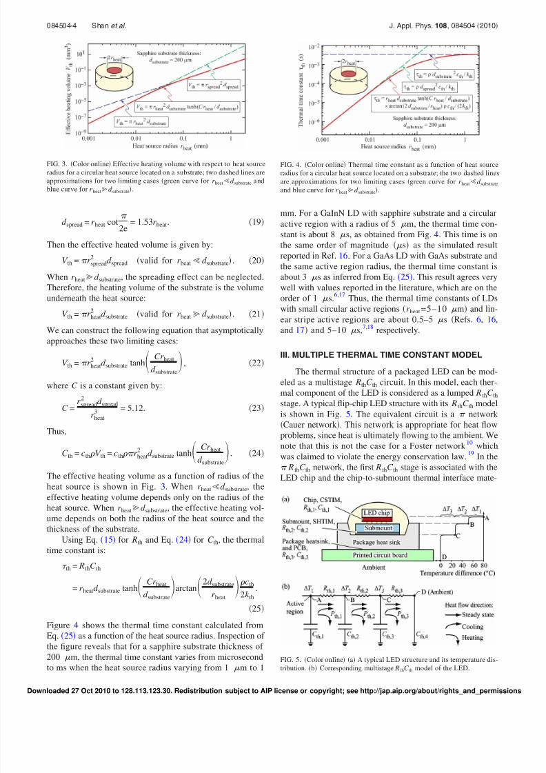
The effective heating volume as a function of radius of theheat source is shown in Fig. 3. When r heatd substrate, theeffective heating volume depends only on the radius of theheat source. When r heatd substrate, the effective heating vol-ume depends on both the radius of the heat source and thethickness of the substrate.
Using Eq. 15 for Rth and Eq. 24 for C th, the thermaltime constant is:
th = RthC th
= r heatd substrate tanh Cr heat
d substratearctan2d substrate
r heat cth
2k th.
25
Figure 4 shows the thermal time constant calculated fromEq. 25 as a function of the heat source radius. Inspection of the figure reveals that for a sapphire substrate thickness of 200 m, the thermal time constant varies from microsecondto ms when the heat source radius varying from 1 m to 1
mm. For a GaInN LD with sapphire substrate and a circularactive region with a radius of 5 m, the thermal time con-stant is about 8 s, as obtained from Fig. 4. This time is onthe same order of magnitude s as the simulated resultreported in Ref. 16. For a GaAs LD with GaAs substrate and
the same active region radius, the thermal time constant isabout 3 s as inferred from Eq. 25. This result agrees verywell with values reported in the literature, which are on theorder of 1 s.6,17 Thus, the thermal time constants of LDswith small circular active regions r heat=5–10 m and lin-ear stripe active regions are about 0.5–5 s Refs. 6, 16,and 17 and 5–10 s,7,18 respectively.
III. MULTIPLE THERMAL TIME CONSTANT MODEL
The thermal structure of a packaged LED can be mod-eled as a multistage RthC th circuit. In this model, each ther-mal component of the LED is considered as a lumped R thC th
stage. A typical flip-chip LED structure with its R thC th modelis shown in Fig. 5. The equivalent circuit is a networkCauer network. This network is appropriate for heat flowproblems, since heat is ultimately flowing to the ambient. Wenote that this is not the case for a Foster network10 whichwas claimed to violate the energy conservation law.19 In the R thC th network, the first R thC th stage is associated with theLED chip and the chip-to-submount thermal interface mate-
FIG. 3. Color online Effective heating volume with respect to heat sourceradius for a circular heat source located on a substrate; two dashed lines areapproximations for two limiting cases green curve for r heatd substrate andblue curve for r heatd substrate.
FIG. 4. Color online Thermal time constant as a function of heat sourceradius for a circular heat source located on a substrate; the two dashed linesare approximations for two limiting cases green curve for r heatd substrate
and blue curve for r heatd substrate.
FIG. 5. Color online a A typical LED structure and its temperature dis-tribution. b Corresponding multistage R thC th model of the LED.
084504-4 Shan et al. J. Appl. Phys. 108, 084504 2010
Downloaded 27 Oct 2010 to 128.113.123.30. Redistribution subject to AIP license or copyright; see http://jap.aip.org/about/rights_and_permissio

7/25/2019 2010 Shan Qifeng Et Al (JAP) Analysis of Thermal Properties of GaInN LEDs and LDs
http://slidepdf.com/reader/full/2010-shan-qifeng-et-al-jap-analysis-of-thermal-properties-of-gainn-leds-and 5/8
rial CSTIM. CSTIM is composed of gold bumps connect-ing the chip and the Si submount. In the first stage, the ther-mal resistance is Rth,1 = Rth,chip + Rth,CSTIM and the thermalcapacitance C th,1 = C th,chip. The thermal capacitance of CSTIM is ignored due to the small volume of the goldbumps compared with that of the LED chip. The second RthC th stage is associated with the submount and thesubmount-to-heat-sink thermal interface material SHTIM.
The SHTIM has a much smaller volume than that of the Sisubmount. Thus, Rth,2 = Rth,Submount+ Rth,SHTIM and C th,2
= C th,submount. The third RthC th stage is associated with thepackage heat sink and the printed circuit board PCB. Andwe have Rth,3 = Rth,heat sink+PCB+ Rth,convection and C th,3
= C th,heat sink+PCB. We note that Fig. 5 shows no capacitor be-tween the PCB and the ambient. This is due to the fact thatthe ambient has an infinitely large thermal capacitance. Wecan represent an infinitely large capacitor by a short circuitsince:
Z th = 1
i C th→ 0 for C th→. 26
Székely19 showed by network transformation that thetransient thermal response, after power is switched off, canbe expressed by a sum of exponential terms:
T = i=1
n
T i exp− t
th,i . 27
Note that for the general case, the thermal time constant th,i
is not simply th,i = Rth,iC th,i but is determined by the whole RthC th circuit. However, in typical LED structures, the ther-mal capacitances usually satisfy the following relation:
C th,1 C th,2 C th,3C th,4 . 28
This is because the volume of the component associated witheach thermal capacitance becomes increasingly bigger LEDchip, Si submount, heat sink, PCB board, etc.. On the otherhand, for a reasonable design of an LED, the thermal resis-tances of different stages should be on the same order of magnitude, that is,
Rth,1 Rth,2 Rth,3 Rth,4 , 29
so that there is no “bottleneck” effect that would stronglyimpede the heat flow. Thus, we have,
Rth,1C th,1 Rth,2C th,2 Rth,3C th,3 Rth,4C th,4 . 30
With this condition, it will be proven in the Appendix thatthe time constant of each exponential term is approximatelyequal to th,i = Rth,iC th,i. Schematic illustrations of the junctiontemperature decay on linear time scale and logarithmic timescale are shown in Figs. 6a and 6b, respectively. Figure6b shows that using logarithmic time scale allows one todistinguish between the different thermal time constants. Thedistinct dependence of T on t , particularly the occurrenceof flat regions d T /d logt =0 and the occurrence of strongly sloped regions d T /d logt 0 can be used todetermine the time constants of specific stages and their as-sociated components.
The temperature response after the power is switched oncan be qualitatively explained as follows: in the initial stage,the LED chip is heated up in a very short time. SinceC th,i1C th,1, the thermal capacitors in the following stagescan be considered as a short-circuit connection to theground.20 Therefore, the thermal time constant th,1
= Rth,1C th,1. Subsequently the submount starts to heat up and
this is governed by a much longer thermal time constant,which is dominated by the second RthC th stage; and so on.The transient cooling process can be considered to be analo-gous to the heating process.
IV. EXPERIMENTAL PROCEDURES USED IN THETRANSIENT JUNCTION TEMPERATUREMEASUREMENT
The device under test is a high-power flip-chip LEDwith emission at 395 nm. The structure of the LED packageis shown in Fig. 7. The LED is grown on sapphire substrateby metal-organic vapor-phase epitaxy. The LED consists of a
FIG. 6. Color online Schematic junction temperature decay having threeexponential decay terms after the power is switched off at t =0 on a alinear time scale and b a logarithmic time scale.
FIG. 7. Color online Packaged LED structure consisting of LED chip,submount, and package and its thermal R thC th model.
084504-5 Shan et al. J. Appl. Phys. 108, 084504 2010
Downloaded 27 Oct 2010 to 128.113.123.30. Redistribution subject to AIP license or copyright; see http://jap.aip.org/about/rights_and_permissio

7/25/2019 2010 Shan Qifeng Et Al (JAP) Analysis of Thermal Properties of GaInN LEDs and LDs
http://slidepdf.com/reader/full/2010-shan-qifeng-et-al-jap-analysis-of-thermal-properties-of-gainn-leds-and 6/8
2 m thick undoped GaN layer, a 3 m Si-doped GaNlayer, six-period Si-doped GaInN/GaN multiple quantumwells, a 24 nm Mg-doped AlGaN electron blocking layer, a100 nm Mg-doped p-type GaN, and a 45 nm Mg-dopedp+-type GaN layer. The LED chip is mounted on the siliconsubmount via CSTIM, i.e., the gold bumps. The submounthas a dimension of 220.4 mm3. The SHTIM, which ismade of silver paste, is used to attach the submount and the
heat sink. The heat sink is made of copper coated with alu-minum.In our experiments, the measurement method for the
junction temperature is the forward-voltage method.2 Thismethod includes two steps. In the first step, the sample isplaced in a temperature controlled oven. For different oventemperatures, the forward voltage is measured at an injectioncurrent of 10 mA, which is the “probe current” to be used inthe second step. The probe current is low enough so that the junction temperature remains the same as the oven tempera-ture. In the second step, the forward voltage of the device ismeasured at the probe current. The junction temperature of the device is then determined by using the calibration data
obtained in the first step.By a linear fit of the V f versus T oven curve from the first
step, the temperature coefficient dV f /dT is obtained for aprobe current of 10 mA. For our measurement, the tempera-ture coefficient is determined to be 1.84 mV/K, which is ina good agreement with the theoretical calculation reported inRef. 2. In the transient junction temperature measurement,we attach the LED package to a large copper block so thatthe temperature of the package heat sink is at room tempera-ture. Currents with pulse duration of 200 ms i.e., quasi-dcand period of 1 s are injected into the sample. The currentsvary from 200 to 800 mA with an increment of 100 mA. 200ms is experimentally proven to be much longer than the time
required for heating the device to the steady state. During thecooling period, we apply a probe current of 10 mA. Thisprobe current does not induce significant heat to the junctionand thus will not influence the temperature during cooling.The junction temperature is obtained from the calibrated for-ward voltage at the probe current.
V. EXPERIMENTAL RESULTS ANALYSIS
Figure 8 shows the transient junction temperature re-sponse after the power is switched off. The quasi-dc currentsrange between 200 and 800 mA. We use a logarithmic time
scale as abscissa, which can show very different time con-stants in one diagram. The experimental data is fitted by asingle exponential function as well as multiexponential func-tions. We found that a single exponential function does not fitthe experimental data well. Therefore, we fit the experimen-tal results by the following function which has two exponen-tial terms:
T t = T 1 exp− t
th,1 + T 2 exp−
t
th,2 . 31
Four fitting parameters are used to fit the equation to theexperimental data: T 1, T 2, th,1, and th,2. The theoreticalfits are also shown in Fig. 8. Inspection of the figure reveals
that the experimental data is fitted very well by the equation.The four fitting parameters as a function of current are
shown in Fig. 9. It is found that T 1 and T 2 monotonically
increase with current. However, the ratio of
T 2 and
T 1does not change much with current. The average value of T 2 /T 1 is about 3.3. Moreover, th,1 and th,2 vary littlewith current. By averaging the thermal time constants overdifferent currents, we obtain the two thermal time constants: th,1 =2.72 ms0.68 ms and th,2 =18.8 ms0.8 ms. Thisindicates that, as expected, the thermal properties of the LEDare determined by the thermal resistance and the thermalcapacitance of the materials and not by the input power. Thetwo time constants obtained from the fitting, th,1 and th,2,are considered as the times required for cooling down orheating up the chip and the submount, respectively.
Figure 10 shows the steady-state junction temperature at
t 0 before the power is switched off versus the inputpower. The linear fit of the junction temperature versus theinput power yields an approximate thermal resistance of 12.2 K W−1 from the chip to the package heat sink. FromEqs. A12, A13 and A14, the following fitting param-eters of the two stage RthC th circuit are extracted: Rth,1
=2.83 K W−1, Rth,2 =9.39 K W−1, C th,1 =0.962 mJ K−1 andC th,2 =2.00 mJ K−1. The calculated thermal capacitances of the chip and the Si submount are 0.652 mJ K−1 chip: V
FIG. 8. Color online Measured temperature decay curves for differentdrive currents of a GaInN LED. The LED drive current is switched off att =0. The solid lines are fitting curves that closely match the experimentaldata. The fitting curves consist of two exponential terms.
FIG. 9. Color online Measured temperature differences between activeregion and submount T 1 and submount and package heat sink T 2 of apackaged GaInN LED as a function of the injection current. Also shown arethe associated thermal time constants, as extracted from the temperaturedecay curves.
084504-6 Shan et al. J. Appl. Phys. 108, 084504 2010
Downloaded 27 Oct 2010 to 128.113.123.30. Redistribution subject to AIP license or copyright; see http://jap.aip.org/about/rights_and_permissio

7/25/2019 2010 Shan Qifeng Et Al (JAP) Analysis of Thermal Properties of GaInN LEDs and LDs
http://slidepdf.com/reader/full/2010-shan-qifeng-et-al-jap-analysis-of-thermal-properties-of-gainn-leds-and 7/8

7/25/2019 2010 Shan Qifeng Et Al (JAP) Analysis of Thermal Properties of GaInN LEDs and LDs
http://slidepdf.com/reader/full/2010-shan-qifeng-et-al-jap-analysis-of-thermal-properties-of-gainn-leds-and 8/8
Rth,2 Rth,1 , A7
we obtain:
1
th,1+
1
th,22
= 1
Rth,2C th,2+
1
Rth,1C th,2+
1
Rth,1C th,12
1
Rth,1C th,12
= 1
Rth,1C th,1 Rth,1C th,1
1
Rth,1C th,1 Rth,2C th,2=
1
th,1
1
th.2. A8
Therefore
1
th,1+
1
th,22
1
th,1
1
th,2. A9
If the two capacitances are very different, we can write
1
th,1+
1
th,22
4 1
th,1
1
th,2. A10
If the two time constants were the same, then both sides of the equation would be identical. However, since the inequal-ity mandates that the two sides are very different, it impliesthat the two time constants are very different from eachother. Therefore we assume:
th,2 th,1 . A11
From Eq. A4 and using Eq. A6, we obtain
1
th,1
1
Rth,2C th,2+
1
Rth,1C th,2+
1
Rth,1C th,1
1
Rth,1C th,1.
A12
Furthermore, by using Eq. A5, we obtain:1
th,2
1
Rth,2C th,2. A13
Using Eqs. A12 and A13, the solution of Eq. A2 can bewritten as:
T t = T 1 exp− t
th,1 + T 2 exp−
t
th,2 , A14
where T 1 and T 2 are the steady-state temperature dropsacross Rth,1 and Rth,2, respectively.
For an R thC th network with the number of stages greater
than 2, we can make the following approximation during thecooling down or heating up of the ith stage: The impedanceof the jth capacitor j i is given by
Z th, j = 1
i C th, j→ 0, when C th, j C th,i . A15
Therefore, we approximate the capacitor after the ith stage,i.e., the jth stage, as short-circuit connection to ground.Therefore, the contribution of C j on the cooling of the ithstage can be neglected. Then the time constant of the ith RC
cell is just
th,i Rth,iC th,i . A16
Furthermore, the temperature decay function can be writtenas:
T t = i=1
n
T i exp− t
th,i . A17
The heating transient response has the same characteristicequation of the thermal time constant as Eq. A3. This indi-cates that the heating response function is given by:
T t = i=1
n
T i1 − exp− t
th,i . A18
1E. F. Schubert, Light-Emitting Diodes, 2nd ed. Cambridge UniversityPress, Cambridge, 2006.
2Y. Xi and E. F. Schubert, Appl. Phys. Lett. 85, 2163 2004.3Y. Xi, J.-Q. Xi, Th. Gessmann, J. M. Shah, J. K. Kim, E. F. Schubert, A.J. Fischer, M. H. Crawford, K. H. A. Bogart, and A. A. Allerman, Appl.Phys. Lett. 86, 031907 2005.
4N. C. Chen, Y. K. Yang, Y. N. Wang, and Y. C. Huang, Appl. Phys. Lett.90, 181104 2007.
5P. Vitta and A. Žukauskas, Appl. Phys. Lett. 93, 103508 2008.6G. Hasnain, K. Tai, L. Yang, Y. H. Wang, R. J. Fischer, J. D. Wynn, B.Weir, N. K. Dutta, and A. Y. Cho, IEEE J. Quantum Electron. 27, 13771991.
7C. Eichler, S.-S. Schad, M. Seyboth, F. Habel, M. Scherer, S. Miller, A.Weimar, A. Lell, V. Härle, and D. Hofstetter, Phys. Status Solidi C 7, 22832003.
8Z. Gong, M. Gaevski, V. Adivarahan, W. Sun, M. Shatalov, and M. Asif Khan, Appl. Phys. Lett. 88, 121106 2006.
9V. S. Arpaci, Conduction Heat Transfer Addison-Wesley, Reading, Mas-sachusetts, 1966.
10P. Vitta and A. Žukauskas, Phys. Status Solidi C 6, S877 2009.11I. N. Sneddon, Mixed Boundary Value Problems in Potential Theory
Wiley, New York, 1966.12C. J. Tranter, Integral Transforms in Mathematical Physics Wiley, New
York, 1966.13R. H. Cox and H. Strack, Solid-State Electron. 10, 1213 1967.14B. Gelmont and M. Shur, Solid-State Electron. 36, 143 1993.15M. W. Denhoff, J. Phys. D 39, 1761 2006.16J. Piprek, Proc. SPIE 6013, 60130B 2005.17P. V. Mena, J. J. Morikuni, S.-M. Kang, A. V. Harton, and K. W. Wyatt, J.
Lightwave Technol. 17, 865 1999.18R. D. Esman and D. L. Rode, J. Appl. Phys. 59, 407 1985.19V. Székely, Microelectron. J. 28, 277 1997.20F. N. Masana, Microelectron. Reliab. 41, 901 2001.
084504-8 Shan et al. J. Appl. Phys. 108, 084504 2010