2. circuit implementation of the transfer function
TRANSCRIPT

2. Circuit implementation of the transfer function
Kanazawa UniversityMicroelectronics Research Lab.Akio Kitagawa
2.1 Block diagram of continuous-time circuit
2

3
Linear elements for continuous-time circuit
s
/s
In1
In2
Out
Out
Out
In
In
Adder and subtractor
Differentiator
Integrator
The parameters , , and are the gain of an amplifier, a differentiator, and an integrator, respectively.
OutInConstant multiplication

4
)()()(1)(
outinoutinoutinout
inout
in
out
VVs
VcVbs
VcVbs
V
VbVcscsb
VV
Block diagram of 1st-order LPF
csbVin Vout =
scsb
VVsHin
out)(
cb
Transfer function
/s VoutVin
NOTE: A feedback of a constant introduces a constant term in a denominator.
Block diagram of transfer function

5
Block diagram of 1st-order HPF
cssa
Vin Vout =
s
scssa
VVsHin
out)(
ca
/s VoutsVin
)()()(1)(
outinoutinoutinout
inout
in
out
VVss
VcVsas
VcVsas
V
VsaVcscssa
VV
Transfer function Block diagram of transfer function

6
)()()(1)()(
outininoutininoutininout
inout
in
out
VVVss
VcVbVsas
VcVbVsas
V
VbsaVcscsbsa
VV
Block diagram of 1st-order transfer function
csbsa
Vin Vout=
ss
csbsa
VVsHin
out)(
cba
/s Vout
sVin
Transfer function
Block diagram of transfer function

7
})({})({
})(1{1)(1)(
1001
10101
01
2
2
2
outoutinoutoutin
outoutinoutoutinout
inout
in
out
VVVss
VdVeVcss
VdVeVcss
VeVsdVcs
V
VcVesds
esdsc
VV
Block diagram of 2nd-order LPF 1esds
c2Vin Vout
010112
102)(
ssesds
cVVsHin
out
010
11
10
edc
/s VoutVin/s
NOTE: A feedback element 0 introduces a constant term in a denominator, and 1makes a design flexibility.

8
Block diagram of 2nd-order LPF 2esds
c2Vin Vout
010112
102)(
ssesds
cVVsHin
out
010
10
10
edc
11Vs
Vout
/s VoutVin
/s
V1
)()(
)()(1)(
01101
011
001
01
011001
012
2
2
outinoutin
outoutinoutoutinout
inout
in
out
VVVss
VeVdVcss
VeVsdVcss
VeVsdVcs
V
VcVesds
esdsc
VV
NOTE: This is another solution of 2nd-order LPF.

9
Block diagram of 2nd-order LPF 3esds
c2Vin Vout
1010
210
2)(ssesds
cVVsHin
out
10
10
10
edc
Vout
s
/sVin/s
)(
)(
)(1
10
101010
10
2
outoutin
outoutin
outoutinout
VVsVss
VeVsdVcss
VeVsdVcs
V

10
)()(
)()(
)(1)(1
0010
111
010
1010
10
11
1
10
10
22
2
2
2
outoutininin
outoutininin
outoutinininout
in
out
VVsss
VVss
Vss
VeVsdss
VbVsas
Vcss
VeVsds
VcVsbVsas
V
esdscsbsa
VV
Block diagram of 2nd-order transfer function
010
110
010
11
11
edcba
esdscsbsa
2
2
VoutVin
Vout
s
/sVin /s
s

11
Stability of higher order transfer function
• A 2-stage-cascade connection of the integrators or differentiators can cause instability of the circuit with the feedback loop, because of the phase rotation > . In the worst case, the circuit unexpectedly oscillates.
log
-
|HI()|(dB)
-20dB
Bode diagram of integrator
The feedback loop with the phase shift > causes the negative feedback (NFB) or positive feedback (PFB).
1st stage2nd stage
log-/2
∠𝐻 𝜔
12
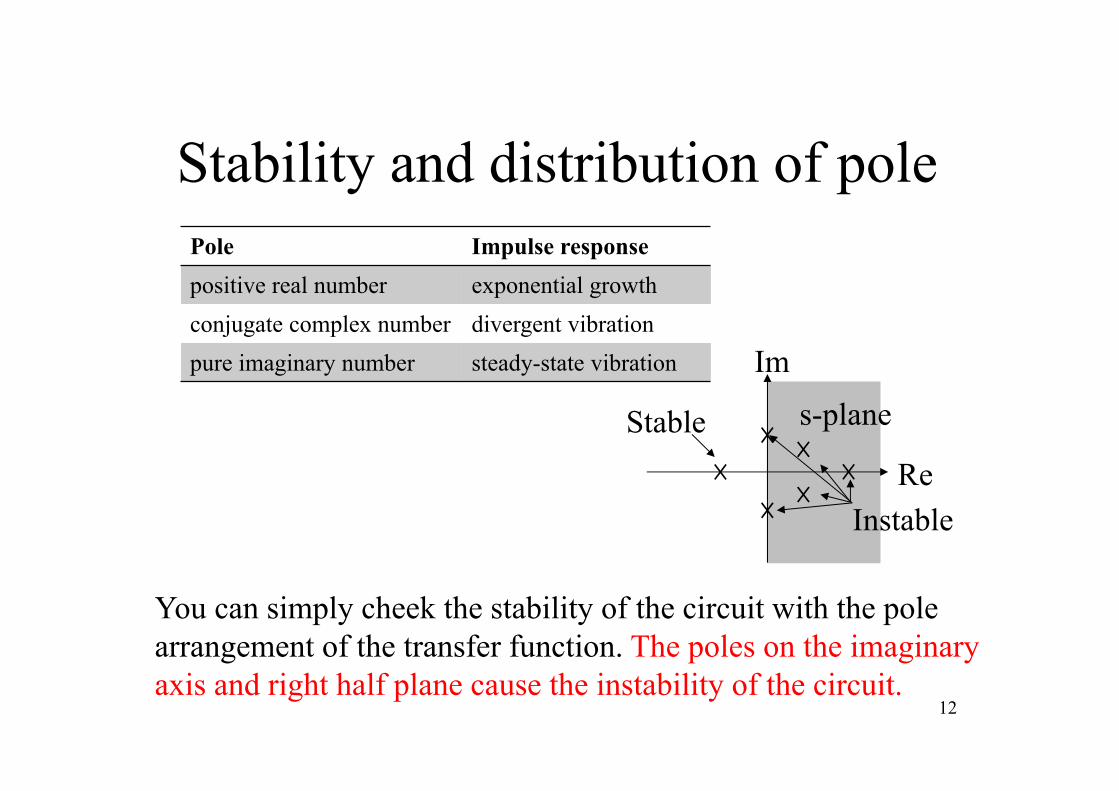
Stability and distribution of pole
You can simply cheek the stability of the circuit with the pole arrangement of the transfer function. The poles on the imaginary axis and right half plane cause the instability of the circuit.
s-plane
Re
Im
Stable
Instable
Pole Impulse responsepositive real number exponential growthconjugate complex number divergent vibrationpure imaginary number steady‐state vibration

2.2 Block diagram of discrete-time circuit
13

14
Integrator and differentiator (1)Integrator by BET Differentiator by BET
)(1
)()(
1)()(
)()()(
1
1
1
zVzTzVTzV
zzVzV
zVzzVzV
inS
XSout
inX
XinX
)(1)(1
zVTzzV inS
out
)(
1)( 1 zV
zTzV inS
out
)(1
)}()({1)(
)()(
1
1
1
zVTz
zVzVzT
zV
zVzzV
inS
ininS
out
inY
z-1
Vin(z) Vout(z)VX(z)
TS
z-1
Vin(z) Vout(z)
VY(z)
1/TS
-
+

15
Integrator and differentiator (2)Integrator by bilinear transform Differentiator by bilinear transform
)(11
2)(
2)(
)()1()()1(
)()()1()(
1
1
11
11
zVzzTzVTzV
zVzzVz
zVzzVzzV
inS
XS
out
inX
XinX
)(112)( 1
1
zVzz
TzV in
Sout
)(11
2)( 1
1
zVzzTzV in
Sout
)(112)(2)(
)()1()()1(
)()()1()(
1
1
11
11
zVzz
TzV
TzV
zVzzVz
zVzzVzzV
inS
XS
out
inX
XinX
z-1
Vin(z) Vout(z)VX(z)
TS/2z-1 z-1
Vin(z) Vout(z)VX(z)
2/TS-
+
z-1
-
-

16
IntegratorIntegrator by FET
)(1
)( 1
1
zVzzTzV in
Sout
TSz-1
1-z-1 Vout(z)Vin(z)
The FET integrator is equivalent to the BET integrator + the delay element of Ts.
z-1Vin(z) Vout(z)VX(z) TS
NOTE: The integrator and delaying integrator show the same characteristic except for delay time. The delaying integrator does not output the hazard generated by the adder.
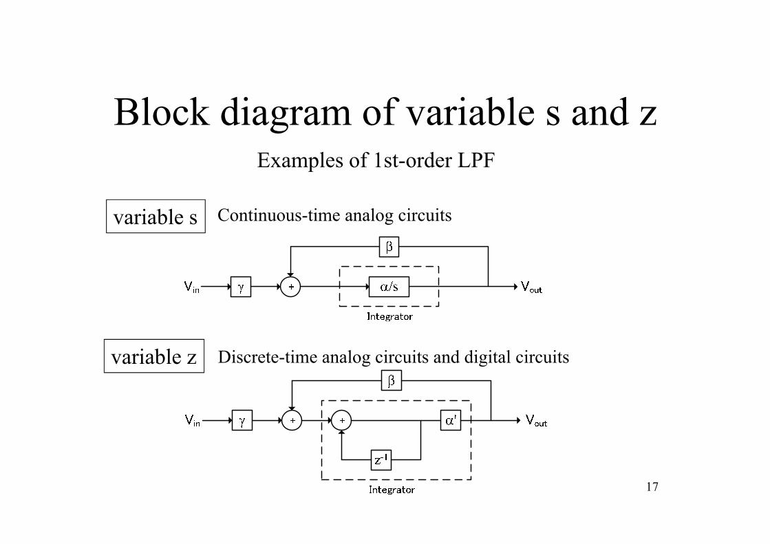
Block diagram of variable s and z
17
Examples of 1st-order LPF
variable s
variable z
Continuous-time analog circuits
Discrete-time analog circuits and digital circuits

2.3 Continuous-time analog implementation
18
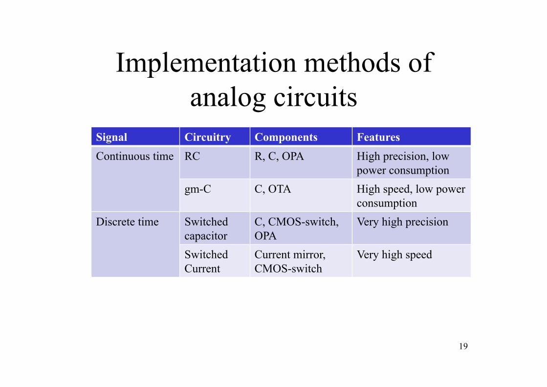
Implementation methods of analog circuits
19
Signal Circuitry Components FeaturesContinuous time RC R, C, OPA High precision, low
power consumptiongm-C C, OTA High speed, low power
consumptionDiscrete time Switched
capacitorC, CMOS-switch, OPA
Very high precision
Switched Current
Current mirror, CMOS-switch
Very high speed

2 types of OPA
)(2
inind
out VVAV
Function
)(2
inind
out VVAV
Ad = Differential Gain
Symbol of Single-end OPA
Symbol of Full-differential OPA
)( inindout VVAV
Ad = Differential Gain
outoutout VVV
20

AC characteristic of OPA
21
1st pole
2nd pole
0dB
Open loop gain
f
f
|Ad(f)|
f)0deg.
-90deg.
Unity gain frequency fu or GBP
Slope = -20dB/Dec.

Linear operators
22
cs
a/s
In1
In2
Out
Out
Out
In
In
Addition and subtraction
Derivation
Integral
(Current summing)
a, b, c : circuit constants
Linear operation elements in the analog circuits
(Capacitor)
(OPA or OTA)
b OutIn (Resistor)Constant factor
(Typical implementation)Operation Symbol

Continuous-time analog operators
23
𝑖 𝑡𝑑𝑞 𝑡𝑑𝑡 𝐶
𝑑𝑣 𝑡𝑑𝑡
ℒ⇒ 𝐼 𝑠 𝑠𝐶 · 𝑉 𝑠
𝑖 𝑡1𝑅 𝑣 𝑡 𝐺𝑣 𝑡
ℒ⇒ 𝐼 𝑠 𝐺 · 𝑉 𝑠
𝑣 𝑡1𝐶 𝑞 𝑡
1𝐶 𝑖 𝜏 𝑑𝜏
ℒ⇒𝑉 𝑠
1𝑠𝐶 𝐼 𝑠
q -q
Constant multiplication
Voltage differentiation
Current integration
q -q

Continuous-time analog integrator (CAI)
24
𝐻 𝑠𝑉 𝑠𝑉 𝑠
𝐺𝐶𝑠
Transfer function of CAI:
I(s)

Implementation example 1
25
𝑉1
𝑠𝐶2 𝑠𝐶1 · 𝑉1𝑅1𝑉
1𝑅2𝑉
𝐻 𝑠𝑉𝑉
𝐶1𝐶2
𝑠 𝐺1𝐶1
𝑠 𝐺2𝐶2
𝑎𝑠 𝑏𝑠 𝑐
G1-1sC2
Vin(s) Vout(s)++
G2sC1
++
++

Full-differential implementation
26
𝐻 𝑠𝑉𝑉
𝐶1𝐶2
𝑠 𝐺1𝐶1
𝑠 𝐺2𝐶2
𝐻 𝑠𝑉𝑉
𝐶1𝐶2
𝑠 𝐺1𝐶1
𝑠 𝐺2𝐶2

Implementation example 2
27
C2G1Vin
+ Vout+
G4
C2
G4
+- +-Vin
- Vout-+
- +-
G1
G3
G3
C1
C1
G2
G2
𝐻 𝑠𝐺1𝐺2𝐶1𝐶2
𝑠 𝐺4𝐶2 𝑠
𝐺2𝐺3𝐶1𝐶2

2.4 Discrete-time analog implementation
28
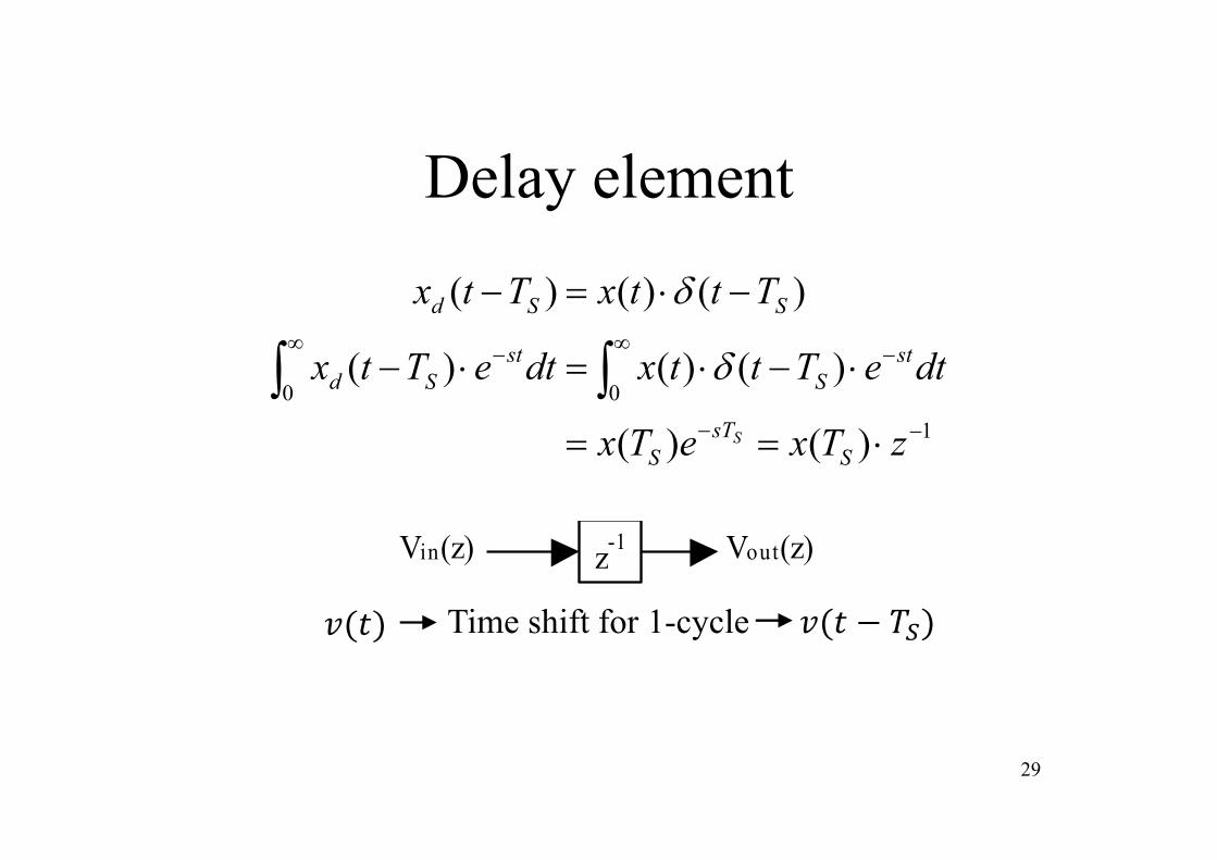
Delay element
29
1
00
)()(
)()()(
)()()(
zTxeTx
dteTttxdteTtx
TttxTtx
SsT
S
stS
stSd
SSd
S
z-1 Vout(z)Vin(z)
𝑣 𝑡 𝑣 𝑡 𝑇Time shift for 1-cycle

Discrete-time analog operators 1
30
𝐼 𝑠 𝑠𝐶 · 𝑉 𝑠 𝐼 𝑧 𝐶 1 𝑧1𝑇 V z
𝑉 𝑠1
𝑠𝐶 𝐼 𝑠 𝑉 𝑧1𝐶
11 𝑧 𝐼 𝑧 𝑇
Voltage differentiation
Charge integration
i(t)
𝑄 𝑧 𝐼 𝑧 𝑇 𝐶 1 𝑧
i(t)
𝑉 𝑧1𝐶
11 𝑧 𝑄 𝑧

Discrete-time analog operators 2
31
Constant multiplication (Switched capacitor)
𝑞 𝑡 𝐶 · 𝑣 𝑡𝑇2
⇒ 𝑄 𝑧 𝐶 · 𝑉 𝑧 𝑧
𝑞 𝑡 𝐶 · 𝑣 𝑡⇒𝑄 𝑧 𝐶 · 𝑉 𝑧
q -q

Non-overlapping clock generator
32
Delay
Delay
1
2
The two-phase clocks 1 and 2 are required to drive the switched capacitor. The edge of clocks 1 and 2 must not overlap, because the leak of the charge stored in capacitors causes the error of the signal processing.

DAI: discrete-time analog integrator 1
33
Positive phase integrator
+- +-
1
1
CM
1
1
CM
in+
in-
out+
out-
Q(z)
𝐻 𝑧𝐶1𝐶2
𝑧1 𝑧

DAI: discrete-time analog integrator 2
34
Opposite phase integrator
+- +-
1 1
CM
1 1
CM
out+
out-
in+
in-
𝐻 𝑧𝐶1𝐶2
11 𝑧
Q(z)

Implementation example
35
+- +-
C11
1
VCM
C11
1
VCM
C2
C3
Vin+
Vin-
Vout+
Vout-
C21 1
VCM
C11 1
VCM
-C1・z-1/2Vin(z) -1C3(1 – z-1)
Vout(z)
C2
++
+
𝐻 𝑧𝑉 𝑧𝑉 𝑧
𝐶1𝐶2 𝐶3
𝑧
𝑧 𝐶3𝐶2 𝐶3
𝑉1𝐶3
11 𝑧 𝐶1𝑧 𝑉 𝐶2 · 𝑉
(LPF)
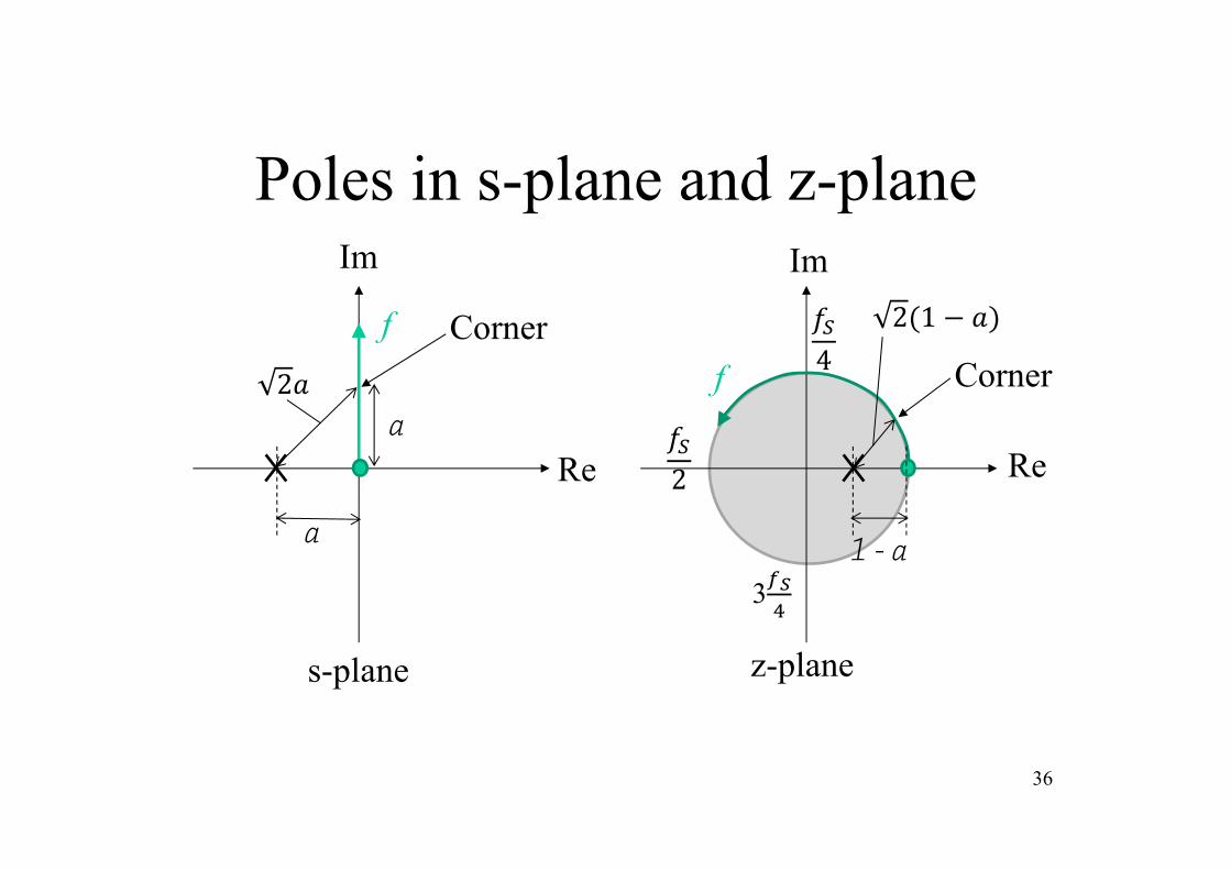
Poles in s-plane and z-plane
36
Re
Im
Re
Im
ff
s-plane z-plane
2 1 𝑎
a
a2𝑎
1 - a
𝑓2
𝑓4
3
CornerCorner

2.5 Digital implementation
37

Digital operators 1
38
Delay
Differentiation (BET)
𝑉 𝑧 1 𝑧 𝑉 𝑧
=
Subtractor

Digital operators 2
39
Integration (BET)
Integration (FET)
𝑉 𝑧 𝑉 𝑧 𝑧 𝑉 𝑧
𝑉 𝑧1
1 𝑧 𝑉 𝑧
𝑉 𝑧 𝑧 𝑉 𝑧 𝑉 𝑧
𝑉 𝑧𝑧
1 𝑧 𝑉 𝑧
Adder
NOTE: The FET integrator does not output the hazards, because the digital delay element is the same as an register.
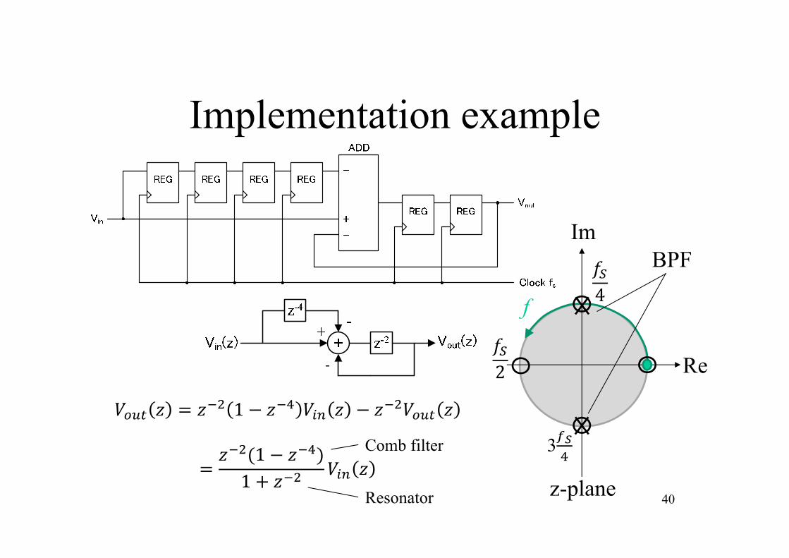
Implementation example
40
𝑉 𝑧 𝑧 1 𝑧 𝑉 𝑧 𝑧 𝑉 𝑧
𝑧 1 𝑧1 𝑧 𝑉 𝑧
Re
Im
f
z-plane
𝑓2
𝑓4
3
Resonator
Comb filter
BPF