19examination subject name: model answer 17534
TRANSCRIPT
MAHARASHTRA STATE BOARD OF TECHNICAL EDUCATION (Autonomous)
(ISO/IEC - 27001 - 2013 Certified)
__________________________________________________________________________________________________
Page 1 /20
WINTER – 19EXAMINATION Subject Name: Microcontroller Model Answer Subject Code:
Important Instructions to examiners: 1) The answers should be examined by key words and not as word-to-word as given in themodel answer scheme. 2) The model answer and the answer written by candidate may vary but the examiner may tryto assess the understanding
level of the candidate. 3) The language errors such as grammatical, spelling errors should not be given moreImportance (Not applicable for
subject English and Communication Skills. 4) While assessing figures, examiner may give credit for principal components indicated in thefigure. The figures drawn by
candidate and model answer may vary. The examiner may give credit for anyequivalent figure drawn. 5) Credits may be given step wise for numerical problems. In some cases, the assumed constantvalues may vary and there
may be some difference in the candidate’s answers and model answer.
6) In case of some questions credit may be given by judgement on part of examiner of relevant answer based on candidate’s understanding.
7) For programming language papers, credit may be given to any other program based on equivalent concept.
Q. No.
Sub Q. N.
Answer Marking Scheme
Q.
1 a) Attempt any THREE of the following: 12- Marks
i) Compare between microprocessor and microcontroller(any four) 4M
17534

MAHARASHTRA STATE BOARD OF TECHNICAL EDUCATION (Autonomous)
(ISO/IEC - 27001 - 2013 Certified)
__________________________________________________________________________________________________
Page 2 /20
Ans:
1M each
(Any four)
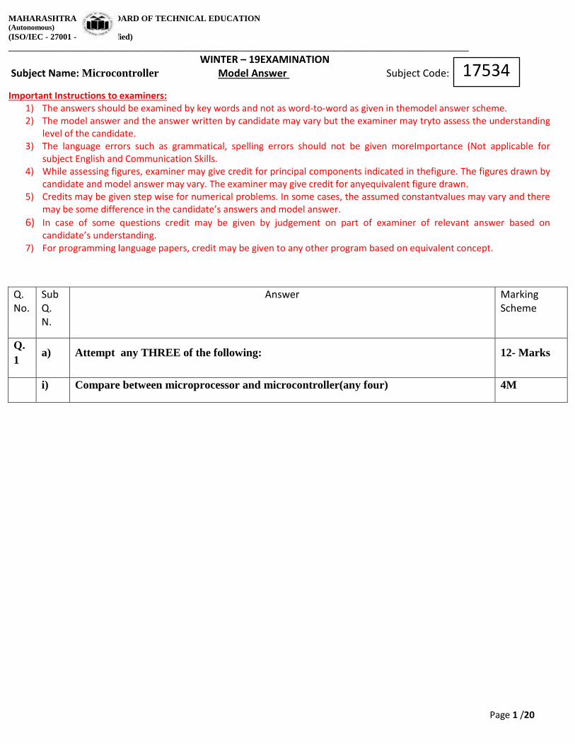
ii) State the difference between Harvard and Von-Neumann architecture with suitable
diagram. 4M
MAHARASHTRA STATE BOARD OF TECHNICAL EDUCATION (Autonomous)
(ISO/IEC - 27001 - 2013 Certified)
__________________________________________________________________________________________________
Page 3 /20
Ans:
4M (Any
four)1M
each
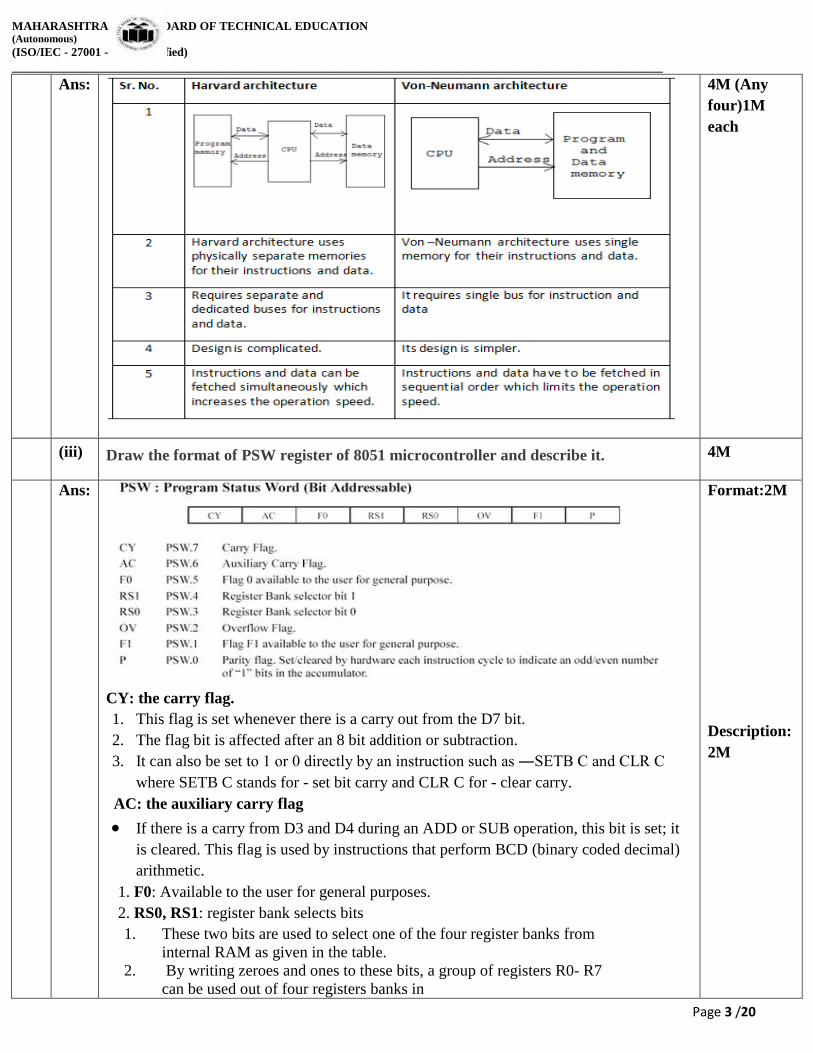
(iii) Draw the format of PSW register of 8051 microcontroller and describe it. 4M
Ans:
CY: the carry flag.
1. This flag is set whenever there is a carry out from the D7 bit.
2. The flag bit is affected after an 8 bit addition or subtraction.
3. It can also be set to 1 or 0 directly by an instruction such as ―SETB C and CLR C
where SETB C stands for - set bit carry and CLR C for - clear carry.
AC: the auxiliary carry flag
If there is a carry from D3 and D4 during an ADD or SUB operation, this bit is set; it
is cleared. This flag is used by instructions that perform BCD (binary coded decimal)
arithmetic.
1. F0: Available to the user for general purposes.
2. RS0, RS1: register bank selects bits
1. These two bits are used to select one of the four register banks from
internal RAM as given in the table. 2. By writing zeroes and ones to these bits, a group of registers R0- R7
can be used out of four registers banks in
Format:2M
Description:
2M

MAHARASHTRA STATE BOARD OF TECHNICAL EDUCATION (Autonomous)
(ISO/IEC - 27001 - 2013 Certified)
__________________________________________________________________________________________________
Page 4 /20
Internal RAM.
3. OV: the overflow flag
This flag is set whenever the result of a signed number operation is too
large, causing the high-order bit to overflow into the sign bit. In
general, the carry flag is used to detect errors in unsigned arithmetic
operations. The overflow flag is only used to detect errors in signed
arithmetic operations.
4. P: Parity flag: The parity flag reflects the number of 1s in the A (accumulator)
register only. If the A register contains an odd number of 1’s, then P=1, P=0 if A has
an even number of 1’
(iv) Explain the function of following directives
(1)DB
(2)EQU
(3)ORG
(4)END
4M
Ans: (1)DB
DB:- (Define Byte)
Syntax: Label: DB Byte
Where byte is an 8-bit number represented in either binary, Hex, decimal or ASCII form.
There should be at least one space between label & DB. The colon (:) must be present after
label. This directive can be used at the beginning of program. The label will be used in
program instead of actual byte. There should be at least one space between DB & a byte.
E.g. LOOKUP: DB 30h,31h,32h,33h,34h,35h.
(2)EQU
EQU: Equate
It is used to define constant without occupying a memory location.
Syntax: Label EQU Numeric value
By means of this directive, a numeric value is replaced by a symbol. For e.g. MAXIMUM
EQU 99 After this directive every appearance of the label ―MAXIMUM in the program,
the assembler will interpret as number 99 (MAXIMUM=99).
(3)ORG
ORG:-ORG stands for Origin
Syntax: ORG Address
The ORG directive is used to indicate the beginning of the address. The number that comes
after ORG can be either in hex or in decimal. If the number is not followed by H, it is
1M each

MAHARASHTRA STATE BOARD OF TECHNICAL EDUCATION (Autonomous)
(ISO/IEC - 27001 - 2013 Certified)
__________________________________________________________________________________________________
Page 5 /20
decimal and the assembler will convert it to hex. Some assemblers use ―.ORG (notice the
dot) instead of ―ORG for the origin directive
(4)END
This directive must be at the end of every program meaning that in the source code
anything after the END directive is ignored by the assembler. This indicates to the
assembler the end of the source file. Once it encounters this directive, the assembler will
stop interpreting program into machine code. e.g. END ; End of the program.
(v) Draw the control word format of 8255 for I/O mode 4M
Ans: Diagram: -
4M
b) Attempt any ONE of the following: 6M
(i) Draw the diagram to interface 2KB,external RAM with 8051 microcontroller,mention
the pins during interfacing and describe in brief. 6M
Ans: Diagram:-
Pins used in interfacing are
1.P0.0-P0.7- Lower order multiplexed address/data bus. It is used to carry lower order
address in the first part of operation and data in the later part.
2.P2.0-P2.7-PORT 2: These are another set of bidirectional input port, they are used when
Diagram:3
M
Pins:1/2M
each

MAHARASHTRA STATE BOARD OF TECHNICAL EDUCATION (Autonomous)
(ISO/IEC - 27001 - 2013 Certified)
__________________________________________________________________________________________________
Page 6 /20
processing external memory to carry higher order address .
3.ALE-Named as Address Latch Enable (ALE). It is used when working with external
memory. When ALE=1, AD0-AD7 contains address and ALE=0, AD0-AD7 contains data.
4.RD-Read data from memory
5.WR- Write data to memory
6.EA-Named as External Access (EA). In order to execute code from internal memory this
pin is connected to Vcc. To execute code from external memory the pin must be grounded.
(ii)
Write a program to multiply two 8 bit numbers stored in internal memory location.
Multiplication is stored in location 40H and multiplier is stored in memory location
41H store LSB of result in R2 and MSNB of result in R3.
6M
Ans: (Note:4 marks for correct program, stepwise marks can be given for
partially correct program, Any suitable address or data can be assumed)
Program:
MOV 40H, # 23H ; store first 8-bit no. in 40H
MOV 41H, #15H ; store second 8-bit no. in
41H
MOV A, 40H ; move first number to A
MOV B, 41H ; move second number to B
MUL AB ; multiply the numbers
MOV R2, A ; move LSB to Reg.R2
MOV R3, B ; move LSB to Reg.R3
HERE: SJMP HERE
6M
Q.2 Attempt any FOUR of the following:
16-Total
Marks
a) Which are different types of Buses? State their features. 4M
Ans: Types of Buses are
1.Address Bus
2.Data Bus
3.Control Bus
Features:
1.Address Bus
Address bus is unidirectional i.e. bits flow in only one direction from the microcontroller to
the peripherals.
The microcontroller with its 16 address lines is capable of addressing2 ^16=65536(64K)
memory locations.
2. Data Bus
Types-
1M
Features-
1M each
b) Draw the format of TCON SFR and explain each bit. 4M

MAHARASHTRA STATE BOARD OF TECHNICAL EDUCATION (Autonomous)
(ISO/IEC - 27001 - 2013 Certified)
__________________________________________________________________________________________________
Page 7 /20
Ans:
TCON SFR
Format:2
M
Explanati
on:2M
c)
Describe the function of following pins of 8051 microcontroller.
(i)PSEN
(ii)EA
(iii)ALE
(iv)RESET
4M
Ans: (i)PSEN
1.PSEN (program store enable). PSEN is the read strobe for external Program Memory. In an
8031-based system in which an external ROM holds the program code, this pin is connected to
the OE pin of the ROM. PSEN is not activated for internal fetches.
(ii)EA
1. EA (external access).EA is pin number 31 in the DIP packages. It is an input pin and must
be connected to either Vcc or GND. It cannot be left unconnected.
2. The lowest 4K bytes of Program Memory can be either in the on-chip ROM or in an
external ROM. This selection is made by connecting EA pin.
1. If the pin is connected to Vcc, then addresses 0000H through 0FFFH are
directed to the internal ROM and addresses 1000H through FFFFH are
directed to external ROM. 2. If the pin is connected to Vss, then all address are directed to external ROM.
(iii)ALE
ALE (Address latch enable). It is an output pin and is active high for latching the low byte of
address during accesses to external memory.
The ALE pin is used for de-multiplexing the address and data by connecting to the STB pin of
the 74LS373 chip.
(iv)RESET
Pin 9 is the Reset Input Pin. This is used for resetting the microcontroller to its initial values. If
1M each
MAHARASHTRA STATE BOARD OF TECHNICAL EDUCATION (Autonomous)
(ISO/IEC - 27001 - 2013 Certified)
__________________________________________________________________________________________________
Page 8 /20
the pin is set at logic 0, the chip runs normally. When the oscillator is running, setting the pin
at logic 1 for more than two machine cycles will reset the microcontroller.
d) State four features of 8051 microcontroller. 4M
Ans: Features of 8051 micro controller are as follows:-
1) 8- bit data bus and 8- bit ALU.
2) 16- bit address bus – can access maximum 64KB of RAM and ROM.
3) On- chip RAM -128 bytes (Data Memory‖)
4) On- chip ROM – 4 KB (Program Memory‖)
5) Four 8-bit bi- directional input/output ports Four 8-bit bi- directional input/ output ports.
6) Programmable serial ports i.e. One UART (serial port)
7) Two 16- bit timers- Timer 0& Timer 1
8) Works on crystal frequency of 11.0592 MHz / 12 MHz
9) Has power saving and idle mode in microcontroller when no operation is performed.
10) Six interrupts are available: Reset, Two interrupts Timers i.e. Timer 0 and Timer 1, two
external hardware interrupts- INT0 and INT1, Serial communication interrupt for both receive
and transmit
Any
Four:1M
each
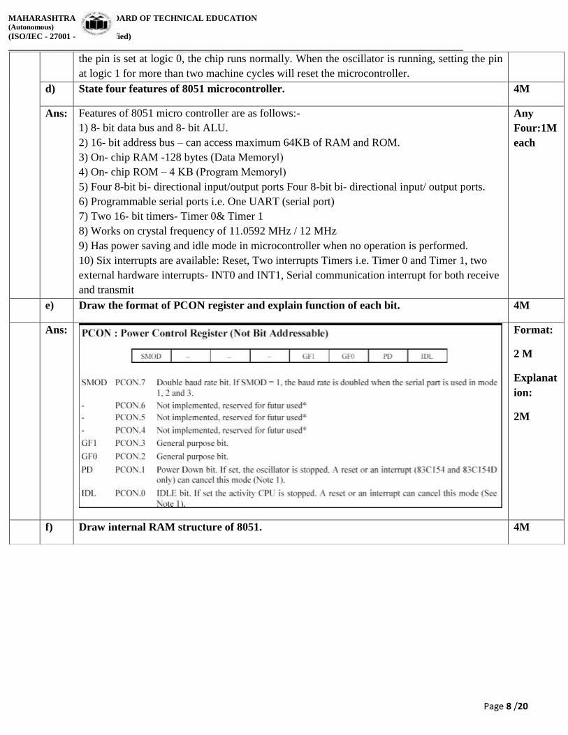
e) Draw the format of PCON register and explain function of each bit. 4M
Ans:
Format:
2 M
Explanat
ion:
2M
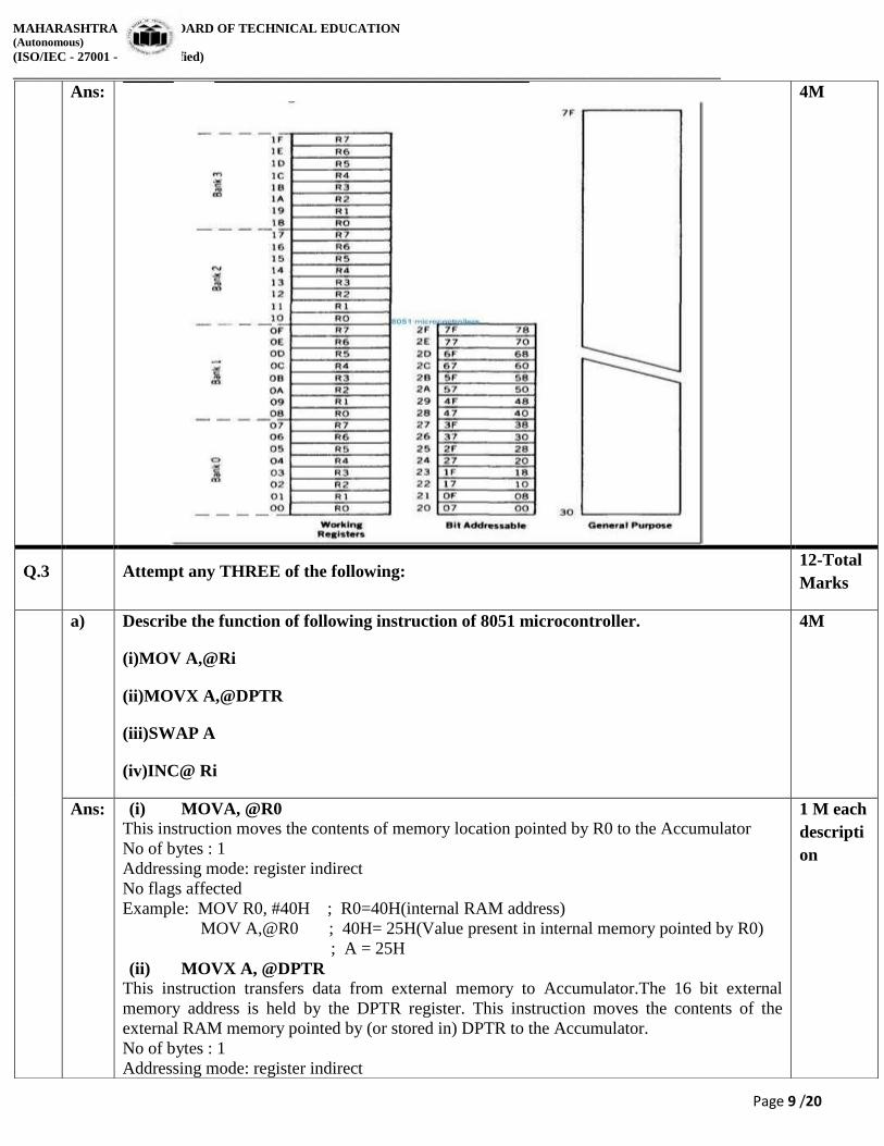
f) Draw internal RAM structure of 8051. 4M
MAHARASHTRA STATE BOARD OF TECHNICAL EDUCATION (Autonomous)
(ISO/IEC - 27001 - 2013 Certified)
__________________________________________________________________________________________________
Page 9 /20
Ans:
4M
Q.3 Attempt any THREE of the following: 12-Total
Marks
a) Describe the function of following instruction of 8051 microcontroller.
(i)MOV A,@Ri
(ii)MOVX A,@DPTR
(iii)SWAP A
(iv)INC@ Ri
4M
Ans: (i) MOVA, @R0
This instruction moves the contents of memory location pointed by R0 to the Accumulator
No of bytes : 1
Addressing mode: register indirect
No flags affected
Example: MOV R0, #40H ; R0=40H(internal RAM address)
MOV A,@R0 ; 40H= 25H(Value present in internal memory pointed by R0)
; A = 25H
(ii) MOVX A, @DPTR
This instruction transfers data from external memory to Accumulator.The 16 bit external
memory address is held by the DPTR register. This instruction moves the contents of the
external RAM memory pointed by (or stored in) DPTR to the Accumulator.
No of bytes : 1
Addressing mode: register indirect
1 M each
descripti
on
MAHARASHTRA STATE BOARD OF TECHNICAL EDUCATION (Autonomous)
(ISO/IEC - 27001 - 2013 Certified)
__________________________________________________________________________________________________
Page 10 /20
Example: MOV DPTR, # 2000H ; DPTR = 2000H(external RAM address)
MOV A, @DPTR ; 2000H=0BH
; A=0BH
(iii) SWAP A
This instruction interchanges bits 0-3 i.e. lower nibble (D0-D3) of the Accumulator with bits
4-7 i.e. upper nibble (D4-D7) of the Accumulator. This instruction is identical to executing
"RR A" or "RL A" four times.
No of bytes: 1 byte
Addressing mode: register specific
Example: MOV A, #59H ;A= 59H ( 0101 1001 in binary)
SWAP A ; A= 95H (1001 0101 in binary)
(iv) INC @Ri
These instruction increments indirect RAM by 1. It increments the contents of memory
location pointed by Ri by 1.
Example: MOV R0, # 40H ; R0 =40H( Sets the memory pointer)
;40H = 05H;
INC @R0 ; Increments contents pointed by R0 by 1
;40H =06H (After execution)
b)
List any two instructions of following addressing modes.
(i)Immediate addressing
(ii)Register addressing
(iii)Direct addressing and
(iv)Index addressing mode
4M
Ans: (i) Immediate addressing mode:
1)MOV A, #25H ; Load 25H into A
2)MOV R2,#05H ;Load 05H into R2
(ii) Register Addressing mode: 1)ADD A, R5 ; Add the contents of register R5 to contents of A (accumulator)
2)MOV R2, A ; Move contents of Accumulator to R2
(iii) Direct Addressing mode:
1) MOV R0, 40H ; Save contents of RAM location 40H in R0.
2) ADD A,50H ; Add contents of memory location 50H &accumulator &store result in
Accumulator.
(iv) Indexed Addressing mode:
1) MOVC A, @A+DPTR
MOVC is a move instruction, which moves data from the external code memory space. The
address operand in this example is formed by adding the content of the DPTR register to the
Accumulator value. Here the DPTR value is referred to as the base address and the
accumulator value us referred to as the index address.
2) MOVC A,@A+PC
1 M
each
addressi
ng ( ½
Mark for
one
example)
c) Write assembly language program to find sum of 5 numbers stored in internal RAM
from memory location 50H.Store result in memory location 70H 4M
Ans: Program for addition of five 8 bit nos.
ORG 0000H
4 M
correct

MAHARASHTRA STATE BOARD OF TECHNICAL EDUCATION (Autonomous)
(ISO/IEC - 27001 - 2013 Certified)
__________________________________________________________________________________________________
Page 11 /20
CLR PSW.3 ; Select register Bank 0
CLR PSW.4 ;
MOV R0, #05H ; Initialize byte counter
MOV R1, #50H ; Initialize memory pointer
MOV A, # 00H ; Clear Accumulator
UP: ADD A @R1 ; Add accumulator with number from array
INC R1 ; Increment memory pointer
DJNZ R0, UP ; Decrement byte counter,
; if byte counter ≠ 0
; Then go to UP if counter is zero then no jump
MOV 70H, A ; Store result in internal memory
HERE: SJMP HERE ; Stop
(Note: Appropriate Marks to be given for any other correct logic used by students.)
program
d) State function of editor, assembler, linker and complier. 4M
Ans: 1) Editor: An editor is a program which helps you to construct your assembly language
program in right format so that the assembler will translate it correctly to machine language.
So, you can type your program using editor. This form of your program is called as source
program and extension of program must be .asm or .src depending on which assembler is used.
The DOS based editor such as EDIT, Wordstar, and Norton Editor etc. can be used to type
your program.
2) Assembler: An assembler is programs that translate assembly language program to the
correct binary code for each instruction i.e. machine code and generate the file called as Object
file with extension .obj and list file with extension .lst extension.
Some examples of assembler are ASEM-51, Keil‟s A51, AX 51 and C51, Intel PL/M-51 etc.
3) Linker: A linker is a program, which combines, if requested, more than one separately
assembled object files into one executable program, such as two or more programs and also
generate .abs file and initializes it with special instructions to facilitate its subsequent loading
the execution.
Some examples of linker are ASEM-51 BL51, Keil u Vision Debugger, LX 51 Enhanced
Linker etc.
4) Compiler: Instructions in assembly language are represented in the form of meaningful
abbreviations, and the process of their compiling into executable code is left over to a special
program on a PC called compiler.
1M
function
of each
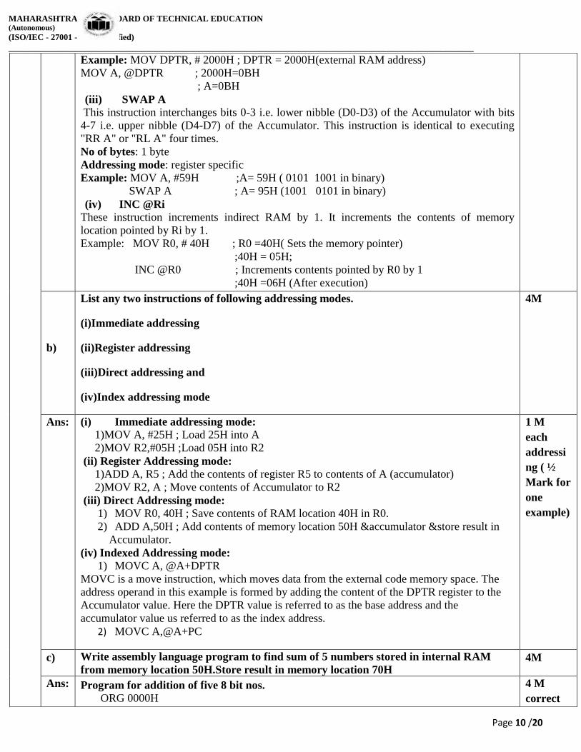
e) Explain the operating mode 1 of serial port of 8051 microcontroller. 4M
Ans: Serial Data Mode-1 (standard UART mode)(baud rate is variable) In mode-1, the serial port functions as a standard Universal Asynchronous Receiver
Transmitter
(UART) mode. 10 bits are transmitted through TXD or received through RXD. The 10 bits
consist of one start bit (which is usually '0'), 8 data bits (LSB is sent first/received first), and a
stop bit (which is usually '1'). Once received, the stop bit goes into RB8 in the special function
register SCON. The baud rate is variable.
3 M
descripti
on
MAHARASHTRA STATE BOARD OF TECHNICAL EDUCATION (Autonomous)
(ISO/IEC - 27001 - 2013 Certified)
__________________________________________________________________________________________________
Page 12 /20
1 Mark
for
formula
Q.4
a)
Attempt any THREE of the following : 12-Total
Marks
(i) Write a program to add two BCD numbers stored in Register R2 and R3 of bank
1.Store result in Register R0 of Bank. 4M
Ans: ORG 0000H
SETB PSW.3 ; Set the bit 3 RS0=1 of PSW
CLR PSW.4 ; Clear bit 4 RS1=0 of PSW to select bank 1
MOV A, R2 ; Load the data from R2 to A
ADD A, R3 ; Add the data present in R3 with Accumulator
DA A ;Adjust the BCD result after addition
MOV R0, A ; Store the result in R0
END ; Stop
(Note: Appropriate Marks to be given for any other correct logic used by students.)
4 Marks
for
correct
program
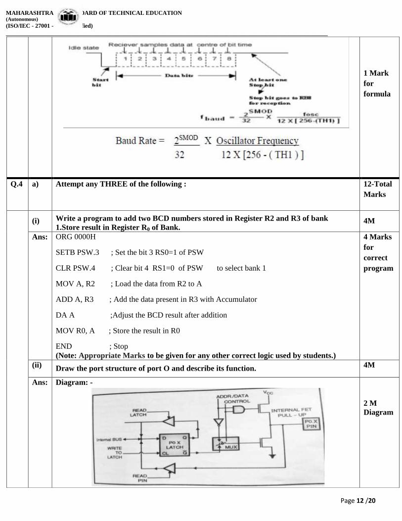
(ii) Draw the port structure of port O and describe its function. 4M
Ans: Diagram: -
2 M
Diagram
MAHARASHTRA STATE BOARD OF TECHNICAL EDUCATION (Autonomous)
(ISO/IEC - 27001 - 2013 Certified)
__________________________________________________________________________________________________
Page 13 /20
Port '0' Port 0 is multi functioned port of microcontroller 8051.Its SFR address is 80H.It is
bit addressable port.
Port 0: It can be used as
a) Simple input/output
b) Bidirectional low order address / data bus (AD0 - AD7 ) for external memory.
When connecting an 8051 to an external memory, port 0 provides both address and data.
The 8051 multiplexes address and data through port 0 to save pins. ALE indicates if P0 has
address or data. When ALE = 0, it provides data D0-D7, but when ALE =1 it has address and
data with the help of a 74LS373 latch
Port 0:
● It is used as input/output or bidirectional low order address and data bus for external
memory. ● It does not have internal pull up resistors. ● When port 0 is used as address/data bus internal control logic switches to address lines to
the gate of FET. ● A logic 1 will turn off lower FET to provide high output at that pin. A logic 0 will turn on
lower FET to provide low output at that pin. ● After the address has been formed ALE signal is used to latch the address and then bus is
turns around to become data bus. Port 0 now reads data from external memory; hence it
must be configured as input. The internal control logic writes logic 1 to all the latches of
port 0.
2M
descripti
on
(iii) What is baud rate in UART of 8051. What value should be loaded into TH1to have 4800
baud rate. Give its decimal and hex value for crystal frequency 11.0592 MH
4M
Ans: Baud rate is a measure of the logic level shifts in a signal per second . It is a measure of the
speed of data transfer, expressed in bits per second (bps).
The baud rate is the rate at which information is transferred in a communication channel. In
the serial port context, "4800 baud" means that the serial port is capable of transferring a
maximum of 4800 bits per second
28800/4800=6 where -6 in decimal=FAH in hex is loaded into TH1.
OR
The count to be loaded in TH1 to have a baud rate of 4800 can be calculated as follows
TH1=256d- [(K*oscillator frequency)/(384d*baud rate)]
Where,
1Mark
for
definitio
n
1 Mark
for
calculati
on
1Mark
each for
decimal
and

MAHARASHTRA STATE BOARD OF TECHNICAL EDUCATION (Autonomous)
(ISO/IEC - 27001 - 2013 Certified)
__________________________________________________________________________________________________
Page 14 /20
SMOD = 0 then K=1 and SMOD = 1 then K=2
Therefore,
TH1=256-[(1*11.0592*106)/(384*4800)]
TH1=250d
TH1=0FAH
hex
value(2
M)
(iv) Write the format of SCON register and explain it. 4M
Ans: Diagram: -
SM0 SM1
0 0 Serial Mode 0
0 1 Serial Mode 1, 8-bit data, 1 stop bit, 1 start bit
1 0 Serial Mode 2
1 1 Serial Mode 3
SM2: enables the multiprocessor communication feature in Modes 2 and 3. In Modes 2 or
3, if SM2 is set to 1 than RI will not be activated if the received 9th date bit(RB8)
is 0. In Mode 1, if SM2 = 1 then RI will not be activated if a valid stop bit was not
Received. In Mode 0 SM2 should be 0.
REN: Receive enable bit. When the REN =1, reception is enabled & REN=0, the
Reception is disabled.
TB8: Transfer bit 8 The 9th data bit that will be transmitted in modes 2 and 3.
RB8: Receive bit 8. The 9th data bit that was received in modes 2 and 3.In mode 1, this bit
is the stop bit that was received.
TI: Transmit interrupt flag. set by hardware at end of 8th bit in mode 0 and at the beginning
of the stop bit in other modes, in serial transmission. Must be cleared by software.
RI: Receive interrupt flag. set by hardware at end of 8th bit in mode 0 and half way through
The stop bit time in other modes in serial reception. Must be cleared by software.
(Note: Make SM2, TB8 and RB8 = 0.)
2 Marks
for
Format
2Marks
for
function
of each
bit
b) Attempt any ONE of the following : 6M
(i) Draw the interfacing diagram of stepper motor with 8051 and write and ALP to rotate
stepper motor continuously in clock wise direction.
Ans: Interfacing diagram
3 Marks
for
interfaci
ng
diagram

MAHARASHTRA STATE BOARD OF TECHNICAL EDUCATION (Autonomous)
(ISO/IEC - 27001 - 2013 Certified)
__________________________________________________________________________________________________
Page 15 /20
OR
Program:
ORG 0000H
MOV A,#66H ;load step sequence
BACK: MOV P1,A ;issue sequence to motor
RRA ;rotate right clockwise
ACALL DELAY ;wait
SJMP BACK ;keep going
DELAY: MOV R2,#100 ;Delay subroutine
3 Marks
for
program
MAHARASHTRA STATE BOARD OF TECHNICAL EDUCATION (Autonomous)
(ISO/IEC - 27001 - 2013 Certified)
__________________________________________________________________________________________________
Page 16 /20
H1: MOV R3,#255
H2: DJNZ R3,H2
DJNZ R2,H1
RET
END
OR ORG 0000H
MOV P1, #00H ; port as output port
MOV R2, #25 ;counter for 1800
rotation(optional as not mentioned in
question for rotation)
UP1: MOV R3, #4 ; counter for full step sequence
MOV DPTR, #TABLE ;load address of program memory into data pointer
UP: CLR A ; clear accumulator
MOVC A, @A+DPTR ; read code from memory into accumulator
MOV P1, A ; send step code to port
ACALL DELAY ;add delay
INC DPTR ; increment memory pointer for next step sequence
DJNZ R3,UP ;decrement counter and repeat from UP till becomes zero
DJNZ R2, UP1 ;decrement counter and repeat from UP1 till becomes zero
SJMP $ ;wait
DELAY: MOV R4,#25 ; delay subroutine
L3: MOV R5,#100
L2: MOV R6,#100
L1: DJNZ R6, L1
DJNZ R5,L2
DJNZ R4,L3
RET
ORG 0050H
TABLE : DB 09H,0CH,06H,03H
END
(Note: Appropriate Marks to be given for any other correct logic used by students.)
(ii) Write a program to move a block of ten bytes stored in internal memory 50H onwards to
external memory location 2000H onwards.
Ans: ORG 0000H
MOV R0,#50H ; Initialize source pointer R0 to 50H
MOV DPTR, #2000H ; Initialize destination pointer DPTR to 2000H
MOV R7,#0AH ;Initialize byte counter
UP: MOV A,@R0 ;Move the contents of first source location to Accumulator
MOVX @DPTR, A ;Move the contents of Accumulator to the first destination
INC R0 ; Increment the content of R0
INC DPTR ; Increment the contents of DPTR
DJNZ R7, UP ; Decrement counter by one and repeat the procedure from UP label ,
If counter becomes zero then no jump to UP
END
(Note: Appropriate Marks to be given for any other correct logic used by students.)
6 Marks
for
correct
program
Q.5
Attempt any FOUR of the following 12 M
(a) Draw the format of TMOD register of 8051 and state function of each bit. 4M

MAHARASHTRA STATE BOARD OF TECHNICAL EDUCATION (Autonomous)
(ISO/IEC - 27001 - 2013 Certified)
__________________________________________________________________________________________________
Page 17 /20
Ans:
2M-
Format,
2M-
Function
(b) Write a program to generate square wave of 1 KHz at P1.5 pin of 8051. Using mode 1 and
timer 0. Assume 12 MHz crystal frequency. 4M
Ans: Calculation:
Timer clock Frequency is = XTAL / 12 = 12 MHz / 12 = 1 MHz
Timer clock period is (Tin)= 1/ Timer Frequency = 1 / 1 MHz = 1 μ sec
For 1 kHz square wave
Fout = 1 KHz
Tout = 1/ (1X 10³
)
Tout =1ms= 1000μ sec
Consider half of it , Tout = 500μ sec
N = Tout / Tin = 500/1 = 500
65536-500= (65036)10 = (FE0C)H
Program:
MOV TMOD, # 01H ; Set timer 0 in Mode 1, i.e., 16 bit timer
L2: MOV TL0, # 0CH ; Load TL register with LSB of count
MOV TH0, # FEH ; load TH register with MSB of count
SETB TR0 ; start timer 0
L1: JNB TF0, L1 ; poll till timer roll over
CLR TR0 ; stop timer 0
CPL P1.5 ; complement port 1.5 line to get high or low
CLR TF0 ; clear timer flag 0
SJMP L2 ; re-load timer with count as mode 1 is not auto reload
1M-
Calculati
on,
1M-
Delay,
2M-
Program
(c) Draw IE register format and explain it. 4M
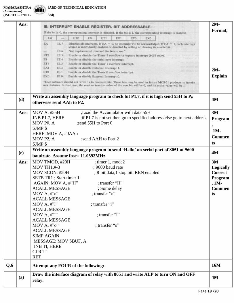
MAHARASHTRA STATE BOARD OF TECHNICAL EDUCATION (Autonomous)
(ISO/IEC - 27001 - 2013 Certified)
__________________________________________________________________________________________________
Page 18 /20
Ans:
2M-
Format,
2M-
Explain
(d) Write an assembly language program to check bit P1.7, if it is high send 55H to P0
otherwise send AAh to P2. 4M
Ans: MOV A, #55H ;Load the Accumulator with data 55H
JNB P1.7, HERE ;if P1.7 is not set then go to specified address else go to next address
MOV P0, A ;send 55H to Port 0
SJMP $
HERE: MOV A, #0AAh
MOV P2, A ;send AAH to Port 2
SJMP $
3M
Program
,
1M-
Commen
ts
(e) Write an assembly language program to send ‘Hello’ on serial port of 8051 at 9600
baudrate. Assume fose= 11.0592MHz. 4M
Ans: MOV TMOD, #20H ; timer 1, mode2
MOV TH1,#-3 ; 9600 baud rate
MOV SCON, #50H ; 8-bit data,1 stop bit, REN enabled
SETB TR1 ; Start timer 1
AGAIN: MOV A, #”H” ; transfer “H”
ACALL MESSAGE ; Some delay
MOV A, #”e” ; transfer “e”
ACALL MESSAGE
MOV A, #”l” ; transfer “l”
ACALL MESSAGE
MOV A, #”l” ; transfer “l”
ACALL MESSAGE
MOV A, #”o” ; transfer “o”
ACALL MESSAGE
SJMP AGAIN
MESSAGE: MOV SBUF, A
JNB TI, HERE
CLR TI
RET
3M
Logically
Correct
Program
, 1M-
Commen
ts
Q.6 Attempt any FOUR of the following: 16M
(a) Draw the interface diagram of relay with 8051 and write ALP to turn ON and OFF
relay. 4M

MAHARASHTRA STATE BOARD OF TECHNICAL EDUCATION (Autonomous)
(ISO/IEC - 27001 - 2013 Certified)
__________________________________________________________________________________________________
Page 19 /20
Ans: Diagram: -
Program AGAIN: SETB P1.0
ACALL DELAY ;Call delay
CLR P1.0
ACALL DELAY ; Call Delay
SJMP AGAIN
SJMP $
DELAY: MOV R2, #0FFH
L1: DJNZ R2, L1
RET
END
2M-
Diagram
2M-
Program
(b) Describe selection factors of microcontroller. 4M
Ans: The selection of microcontroller depends upon the type of application. The following factors
must be considered while selecting the microcontroller.
1. Word length: The word length of microcontroller is either 8, 16 or 32 bit. As the word
length increases, the cost, power dissipation and speed of the microcontroller increases.
2. Power dissipation: It depends upon various factors like clock frequency, speed, supply
voltage, VLSI technology etc. For battery operated embedded systems, we must use low
power microcontrollers.
3. Clock frequency: The speed of an embedded system depends upon the clock frequency.
The clock frequency depends upon the application.
4. Instruction Set: On the basis of instructions microcontrollers are classified into two
categories 1. CISC 2. RISC. CISC system improves software flexibility. Hence it is used in
general purpose systems. RISC improves speed of the system for the particular applications.
5. Internal resources: The internal resources are ROM, RAM, EEPROM, FLASH ROM,
UART, TIMER, watch dog timer, PWM, ADC, DAC, network interface, wireless interface
etc. It depends upon the application for which microcontroller is going to be used.
6. I/O capabilities: The number of I/O ports, size and characteristics of each I/O port, speed
of operation of the I/O port, serial port or parallel ports. These are the considerations needed to
ascertain correct selection of microcontroller.
1M-Each
Any 4
Points
(c) Draw and describe IP register format of 8051. 4M
Ans: FORMAT OF IP:

MAHARASHTRA STATE BOARD OF TECHNICAL EDUCATION (Autonomous)
(ISO/IEC - 27001 - 2013 Certified)
__________________________________________________________________________________________________
Page 20 /20
2M-
Format,
2M-
describe
(d) List the interrupts in 8051. Give their priorities and vector addresses. 4M
Ans:
2M- List,
1M-
Priority,
1M-
vector
address
(e) Explain mode 3 of timer of 8051 with its internal logic diagram. 4M
Ans: Diagram: -
Explain: - In this mode, timer 0 becomes two completed separate 8-bit timers. TL0 is controlled by gate
arrangement of timer 0 and sets timer 0 flag when it overflows. TH0 receives the timer clock
under the control of TR1 bit and sets TF1 flag when it overflows. Timer 1 may be used in
mode 0, 1 and 2 with one important exception that no interrupt will be generated by the timer
when the timer 0 is using TF1 overflow flag.
2M-
Diagram,
2M-
Explain