1997_yang_nanostructured polymer blends - novel materials with enhanced
TRANSCRIPT
7/27/2019 1997_Yang_Nanostructured Polymer Blends - Novel Materials With Enhanced
http://slidepdf.com/reader/full/1997yangnanostructured-polymer-blends-novel-materials-with-enhanced 1/2
ELSEVIER Synth etic Metals 84 (1997) 895-896
Nanostructured polymer blends: novel materials with enhanced optical and electronic propertiesC. Y. Yang, F. Hide, A. J . Heeger, and Y. Cao*
Institute for Polymer and Organic Solids, Universi ty of California, Santa Barbara, CA 93106, USA*UNIAX Corporation, 6780 Cortona Drive , Santa Barbara, CA 93117, USA
Abstract
The morphologies of polymer blends based on MEH-PPV have been studied by using transmission electron microscopy. It is shownthat by controlling the preparation conditions, the phase separation in the blend films results in nano-scale network structure.These nanostructured self assembled polymer blends, as a novel class of materials, offe r enhanced electronic and optical properties.
Keywords: Poly(phenylene vinylene) and derivatives, fulierenes and derivat ives, transmission electron microscopy, bi-continuouspolymer network interfaces
Recent ly, there has been interest in polymer blends andcomposites based on poly[2methoxy-5(2’-ethyl-hexyloxy)-1,4-phenylene vinylene (MEH-PPV); such blends andcomposites offer special or enhanced electronic and opticalproperties. It is important to have knowledge of themorphology and the microstructure of these blend andcomposite materials. Here we summarize recent studies of themorphologies of these materials.The blend films of MEH-PPV with polyquinoline (PQ) andwith polyaniline (PANI) , and the composites of MEH-PPVwith polyethylene oxide (PEO) and with buckminsterfullene(C60) were prepared by spin casting from the relevant
solutions (see refs.l-3) on glass substrates with thicknessaround IOOnm in nitrogen environment. TEM samples wereprepared by the selective dissolution method. Beforedissolution a very thin carbon film (-1Onm) was coated onthe blend film to improve thermal and electricalconductivities for TEM and to avoid breaking the films. Theblend films were floated of f the substrates in water and pickedup on TEM grids, and subsequent ly dried. PQ and PANI blendfilms with MEH-PPV were first deprotonated by using acetonefor more than 24 hours to remove acid counterions. Then, inboth blends with PQ and PANI, the MEH-PPV was dissolvedaway by using chloroform or xylene for more than 24 hoursuntil the films were colorless, i.e. the red orange MEH-PVV
had been dissolved away. TEM samples of composite film ofPEO/MEH-PPV was easy to prepare by dissolving out the PEOin water for several hours. TEM sample o f CeO/MEH-PPV
presented a more diffi cult challenge. Fortunatelydecahydronaphthalene was found to be a suitable selective
solvent for the C&$MEH-PPV system. The microscopy was
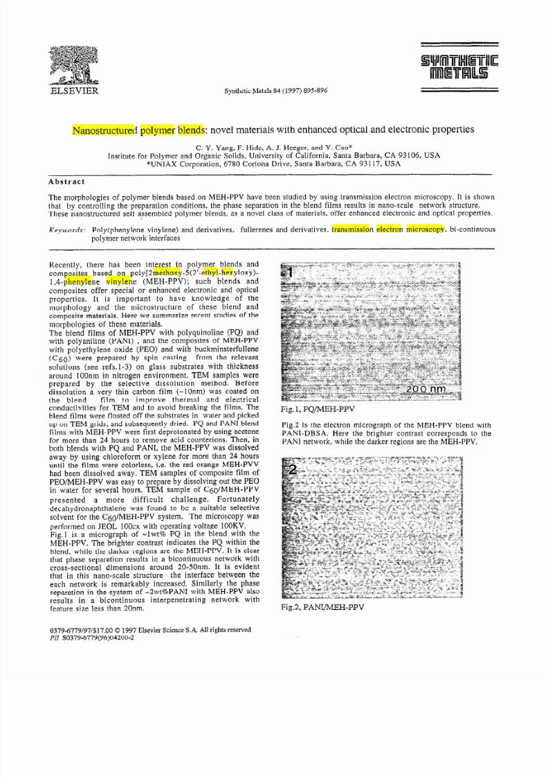
performed on JEOL 1OOcx with operating voltage 100KV.Fig.1 is a micrograph of -lwt% PQ in the blend with theMEH-PPV. The brighter contrast indicates the PQ within the
blend, while the darker regions are the MEH-PPV. It is clearthat phase separation results in a bicontinuous network withcross-sectional dimensions around 20-50nm. It is evidentthat in this nano-scale structure the interface’ between theeach network is remarkably increased. Similarly the phaseseparation in the system of -2wt%PANI with MEH-PPV alsoresults in a bicontinuous interpenetrating network withfeature size less than 20nm.
0379-67791971317.00 8 1997 Elsevier Sc ience S.A All righ ts reserved
PIT SO379-6779(96)04200-2
Fig. 1, PQ/MEH-PPV
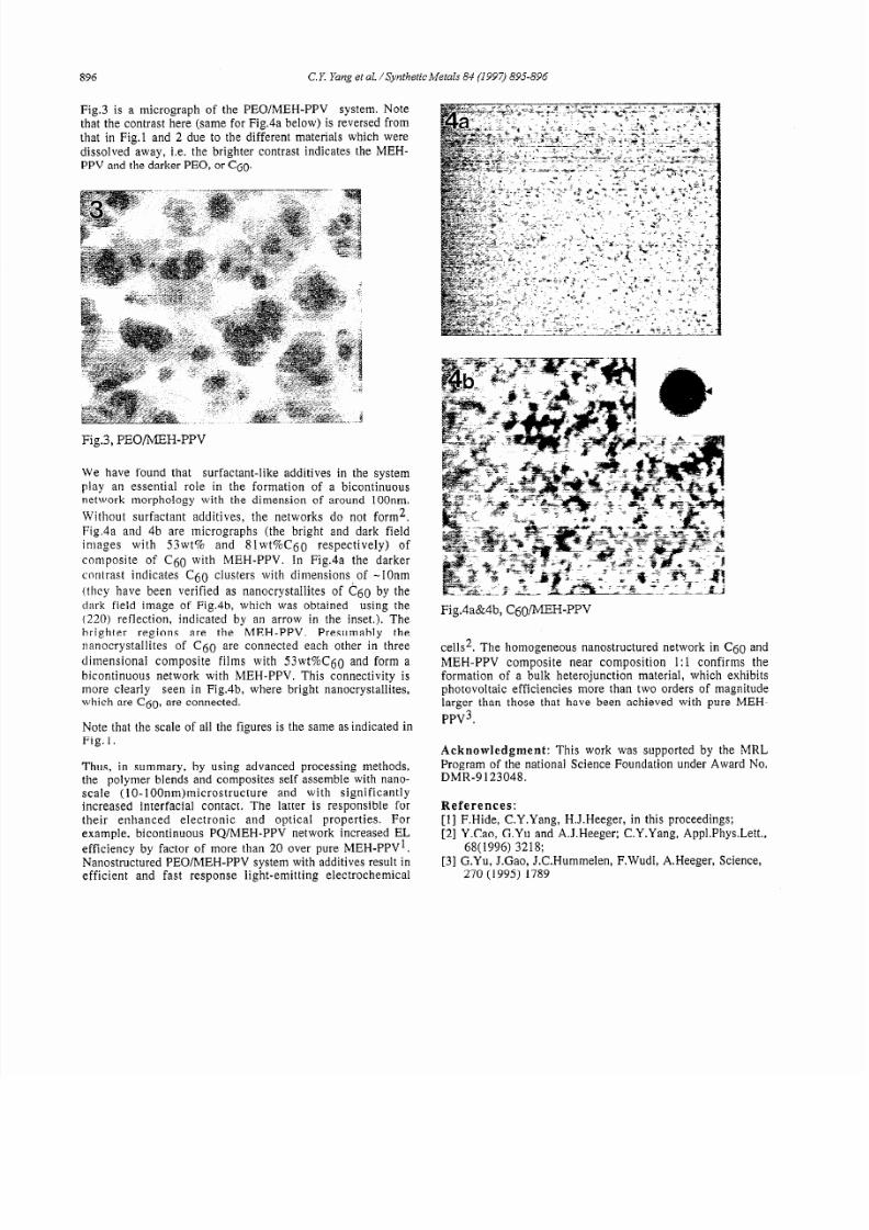
Fig.2 is the electron micrograph of the MEH-PPV blend withPANI-DBSA. Here the brighter contrast corresponds to. thePANI network, while the darker regions are the MEH-PPV.
Fig.2, PA-H-PPV
7/27/2019 1997_Yang_Nanostructured Polymer Blends - Novel Materials With Enhanced
http://slidepdf.com/reader/full/1997yangnanostructured-polymer-blends-novel-materials-with-enhanced 2/2
896 C.Y. Yang et al. /SyntheticMetals 84 (1997) 895-896
Fig.3 is a micrograph of the PEO/MEH-PPV system. Notethat the contrast here (same for Fig.4a below) is reversed fromthat in Fig.1 and 2 due to the different materials which weredissolved away, i.e. the brighter contrast indicates the MEH-PPV and the darker PEO, or C60.
Fig.3, PEO/MEH-PPV
We have found that surfactant-like additives in the systemplay an essential role in the formation of a bicontinuousnetwork morphology with the dimension of around IOOnm.
Without surfactant additives, the networks do not form2.Fig.4a and 4b are micrographs (the bright and dark fieldimages with 53wt% and 8lwt%C60 respectively) ofcomposite of C60 with MEH-PPV. In Fig.4a the darkercontrast indicates C60 clusters with dimensions of -1Onm
(they have been verified as nanocrystallites of C60 by thedark field image of Fig.4b, which was obtained using the(220) reflection, indicated by an arrow in the inset.). Thebrighter regions are the MEH-PPV. Presumably thenanocrystallites of C60 are connected each other in three
dimensional composite films with 53wt%C60 and form abicontinuous network with MEH-PPV. This connectivity ismore clearly seen in Fig.4b, where bright nanocrystallites,which are C60, are connected.
Note that the scale of all the figures is the same as indicated inFig. 1.
Thus, in summary, by using advanced processing methods,the polymer blends and composites self assemble with nano-scale (lo-1OOnm)microstructure and with significantlyincreased interfacial contact. The latter is responsible fortheir enhanced electronic and optical properties. For
example, bicontinuous PQ/MEH-PPV network increased ELefficiency by factor of more than 20 over pure MEH-PPVl.Nanostructured PEOIMEH-PPV system with additives result inefficient and fast response light-emitting electrochemical
Fig.4a&4b, C6@MEH-PPV
cells2. The homogeneous nanostructured network in C60 andMEH-PPV composite near composition 1:l confirms theformation of a bulk heterojunction material, which exhibitsphotovoltaic efficiencies more than two orders of magnitudelarger than those that have been achieved with pure MEH-
PPV3.
Acknowledgment: This work was supported by the MRLProgram of the national Science Foundation under Award No.DMR-9 123048.
References:[I] F.Hide, C.Y.Yang, H.J.Heeger, in this proceedings;
[2] Y.Cao, G.Yu and A.J.Heeger; C.Y.Yang, Appl.Phys.Lett.,68(1996) 3218;[3] G.Yu, J.Gao, J.C.Hummelen, F.Wudl, A.Heeger, Science,
270 (1995) 1789