18~ - georgia institute of technologyece2020.ece.gatech.edu/exams/data/su13-ho-s2.pdf · ece2020...
TRANSCRIPT

-------------------ECE2020 Test 2 Summer 2012 GTL Name: k.EY June 27, 2013 Calculators not allowed. Show your work for any possible par tial credit or in some cases for any credit at all. Note the last page shows you some blank K maps just jn case you need them on this exam. 8 pages, possible 100 points.
Problem 1 Part A (l0 points) Convert the following notations:
Binary representation Hexidecimal representation QO LOl l om 00 00 101 J ~c..95
Signed Binary two's complement represented Decimal 11100.01 - '3.rS Decimal Octal 673 1'2..4-\
Decimal Notation Binary notation 7.75 1\ \. \ \
III DO. 0 I :") C)06Ii.I(J-t I ='> G 00 II. I I-:=>. ') '3 + II + V. 'I. ~ 2
-; 1. '" <013 L-r (.,3 !<-I
If. 8 2 I ~~, P-o
2- r l ~
fAa ~()
4'2.. '2.) '34 P-o
1..1 ,
"2...1 +~ ~o
ID
'2..) ~\ R \
S
:2- J 10 Rfo
"2..
lls RI
I ~o'2.0
0
2ft R. \
/.1 S I \ \. 1 J
I _~ I 'f.. 2
~~ -, S-=
18~
1
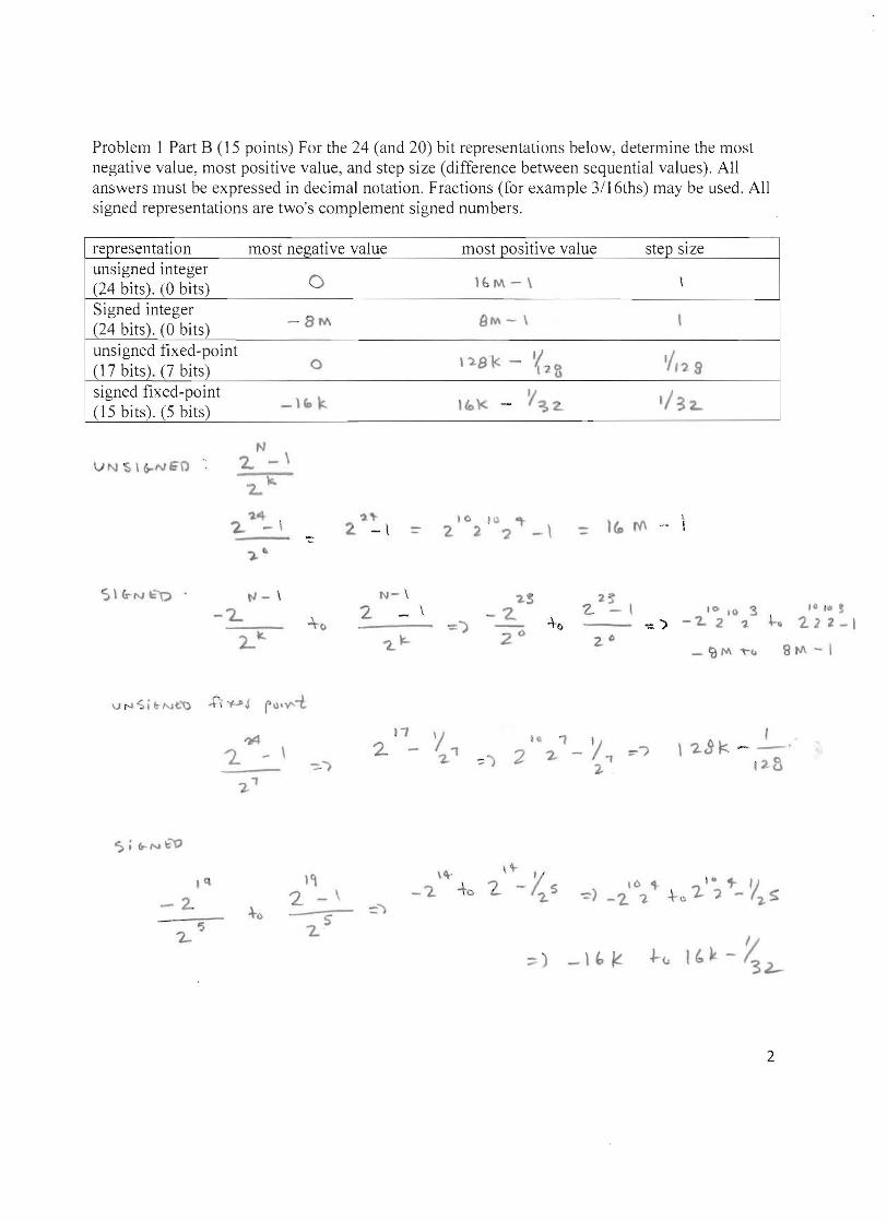
Problem 1 Part B (15 points) For the 24 (and 20) bit representations below, determine the most negative value, most positive value, and step size (difference between sequential values). All answers must be expressed in decimal notation. Fractions (for example 31l6ths) may be used. All signed representations are two's complement signed numbers.
represen tati on most negative value most positive value step size unsigned integer (24 bits). (0 bits) 0 IbM \ \
Signed integer (24 bits). (0 bits) -8M BM - \ , unsigned fixed-point (17 bits). (7 bits) 0 \ '181< - '{'2 ~ '!''l 9 signed fixed-point (15 bits). (5 bits) _1" k 110 l< - Y~2.. 1/32
VN 'S' (,NSO
10 III ~'2." 1(P rI\ =2. - \ 2.. 2 ? -\
.S \ Cr- N '=\.) 1'1- \ N- \ ,$ 2~ 10 10 ~'2.. - I 10 10 3-'2. 2 -'2..-+0 :) +0 -:!. ") - '2.. 2 '2 -h. 1.22_1
2c)2..."'- '2..r- 2./J _ ~ /'II "t-I.> 9J11\-1
17 II) 1 t
'2 2 '2. - 'I, ~I 2..
~,
II\- \~ ~ .., \ '">- S
- &- "To '- '2..-2.
'2..'5
::::)
2

Problem 2 Part A Arithmetic (5 points) For each problem below, compute the operations using the rules of arithmetic, and indicate whether an overflow occurs assuming all numbers are expressed using a six bit unsigned representation
I I
110110 +100110
011001 + 010110
')'" I \ I 0 0 I 0 I , \ I
result o\\\Q() I C\ I I I I
unsigned error? Y N
Problem 2 Part B Arithmetic (10 points) For each problem below, compute the operations using the rules of arithmetic, and indicate whether an overflow occurs assuming all numbers are expressed using a six bit signed two's complement representations.
I I \ I \ I \ 011111 1 1 1 III 011000 001 111
+000100 + 000010 -111011 -0 1 0 1 0 1
I D 0 0 I \ \) 00 () Dol
result \ I.) \) ()' \ D()()Uol 0\\\0\ 1,\ Ill~
signed error?
\ \ \ (J \ \ o I 0 10 I
Ql> ()i 06 , t. I 6 I £) ...... ,
+- \ ouu\o\ \ a I () \ ,
i , \
0\\ 006 00 \ \
() c>o I ~ I o I ~ \ \
o I \ , 0 \ , 0 \ ()
3

3) Given the circuit below: a) (5 points) The designer wants to implement an exclusive-or function where out = Y exclusive-or X. Fill in the values for F3 F2 FI Fo to implement the desired exclusive-or function. b) (5 points) The designer wants to implement the NAND function where out = Y NAND X. Fill in the values for F3 F2 FIFo to implement the desired NAND function. C) (5 points) The designer wants to implement the NOR function where out = Y NOR X. Fill in the values for F3 F2 FIFo to implement the desired N OR function .
function desired: a) exclusive-or
Fl
C
F2
I
FI
b) NAND
c) NOR \ () 0
Fo y f.. t:1- -Oil l'I~p rJO{2.
() 0 D F3 (:)
C
c
CJ
(;)
\
F\
F"L
po 6 0
0
0
Q
OUT
Fa
x y
4
I
C.OV tV",
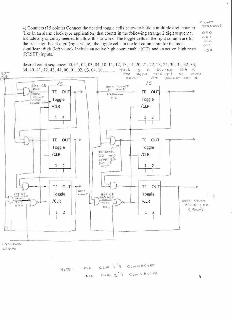
"5E'<ft IJENe..E4) Counters (15 points) Connect the needed toggle cells below to build a multiple digit counter (like in an alarm clock type application) that counts in the following strange 2 digit sequence. 000
Include any circuitry needed to allow this to work. The toggle cells in the right column are for 00 I (lIe
the least significant digit (right value), the toggle cells in the left column are for the most D \ I
significant digit (left value). Include an active high count enable (CE) and an active high reset f 00 (RESET) inputs.
desired count sequence: 00, 01 , 02, 03, 04, 10, 11, 12, 13 , 14, 20, 21 , 22, 23 , 24, 30, 31, 32, 33 , 34, 40,41,42, 43 , 44,00,01 , 02, 03 , 04, 10, .... ..... j\+iS I S A Vlul~~ ~ ~ S
F Oil e.o rl+ D I 6- IT 5 <,;" o(Y\,o~
IS ~ E,TO<ANo JOUT:J mP9< TE (:.ou ,....,-
r;-PuM r ToggleI
L.\I~ 9 1&1
l1D C~
al l
-....~l!D tyl l"")<
E,x.,.- c ~ <ov",-r (>IroItI ,.,~l("
t'Nf)<:Ilu...... N\A-)( <:: <Jo.JNT"
,lt iS V flL~tr""
C.Uu.... '\ Po""t vAt.. ucr Or=- 4-
/5ONI.'I C!(>II foJ'r IF I-lAu ~
~TE OUT ~'#-~ oJ "'4-
c...~ Toggle
r-- /CLR
1 2 I I
~ TE OUT ...
Toggle ~)<'\I::'i!",I\'--
/CLR1"1",-0 .----LIfT'~ slfr
:S I-FI))... 1 2
I I
L TE OUT
E-)CT C. £=- Toggle "'A)C(..0"',..,.,...
'''i~ ~ /CLR (>.6. I,
1 2
I 00'> il> ,.,..
( N Uf"-)1 2
I I I I
,. ...........
/CLR
1 2 I I
~
TE OUT ----r----' Toggle
- /CLR
1 2 I I
\
TE OUTr-
Toggle
/CLR~
N oTE '
5

-------- -------- ---------
---
5) Pliority Encoders (15 points) Given the truth table for the following plioIity encoder:
TN3 TN2 INI TNO 0 0 0 0 1 0 0 0 X 1 0 X X X 1 X X 0 0
OUTI OUTO VALID X X 0 0 1 1 1 0 0 0
a) List the priority order of the inputs IN3, IN2, TNl, INO:
::J:f'I \ > ::fN1..- > :+rJ () > .:f1\l3
highest lowest
b) Using basic gates (AND, OR, NAND, NOR, NOT) show the gate level implementation for this priority encoder.
/""" -./'0 ....,.~
@ , \ I
I \ t \
t \ I I
\ I I \ 1
_\./'-..J::TN l::J -;f N L>
;;:;. . ;tN\ v p.....,p ::: .:I:.t.J3 +- TN'l- -+ -:r t-J ) ~ :iCN 6 :rt'll • ~ NO -\-- .:r"., A .....'1.--DoT \ :: s",....e- f\S
:. fi\ ~ :rNcH-":f" t ) fll... \ '0 -::. ;;:;'3 , ~L . ~, • TIv 0
vS i N (,. NI"N ~
:r"'3 ;r,..?
-- 0 VAL,'" --D0P-:.-.." -l>b7NO - 1)o
1)!1
IN3 ,,,,.1.. I)I~\.-\ )J
I~' tr[) ~ I'" 0
6

6) Registers (15 points) Consider the register implementation below.
A OUT
In Out In Our
IN L.:Itlh L aId }
E1 Ell
W E e1kl clk2
Assume the following signals are applied to your register. Draw the signal at point A (output of the first latch), the signal at point OUT (output of second latch). Assume A and OUT start at unknown values.
Clkl
Clk2
WE
IN
A III kI
1 V.I f ~erL..LZ~1i---,"__.m~---","--,,-.lt OUT III 2 I: Z Z / 27 Z7 ~ j
I
I I I t
7

KMAPS : /B B
/A
A
/A {
A {
/A
A
~
~ /D D /D
/B B
I---+----t--r--i
L----L_-'-----:''-----:-'
/e e /e
/B B
{
{r------r-----,
} /e
e
/e
8