1700 v scale-idriver - power integrations · 1700 v . scale-idriver. this product is covered by...
TRANSCRIPT
www.power.com May 2017
Up to 8 A Single Channel IGBT/MOSFET Gate DriverProviding Basic Galvanic Isolation for 1700 V IGBT and MOSFET
1700 V SCALE-iDriver
This Product is Covered by Patents and/or Pending Patent Applications.
Product HighlightsHighly Integrated, Compact Footprint• Split outputs providing up to 8 A peak drive current• Integrated FluxLink™ technology providing galvanic isolation
between primary-side and secondary-side• Rail-to-rail stabilized output voltage• Unipolar supply voltage for secondary-side• Suitable for 1700 V IGBT and MOSFET switches• Up to 75 kHz switching frequency• Low propagation delay time 260 ns• Propagation delay jitter ±5 ns• -40 °C to 125 °C operating ambient temperature• High common-mode transient immunity• eSOP package with 9.5 mm creepage and clearance distances
Advanced Protection / Safety Features• Undervoltage lock-out protection for primary and secondary-side
(UVLO) and fault feedback• Short-circuit protection using VCE SAT monitoring and fault feedback• Advanced Soft Shut Down (ASSD)
Full Safety and Regulatory Compliance• 100% production partial discharge test• 100% production HIPOT compliance testing at 6 kV RMS 1 s• Basic insulation meets VDE 0884-10
Green Package• Halogen free and RoHS compliant
Applications• General purpose and servo drives• UPS, solar, welding inverters and power supplies
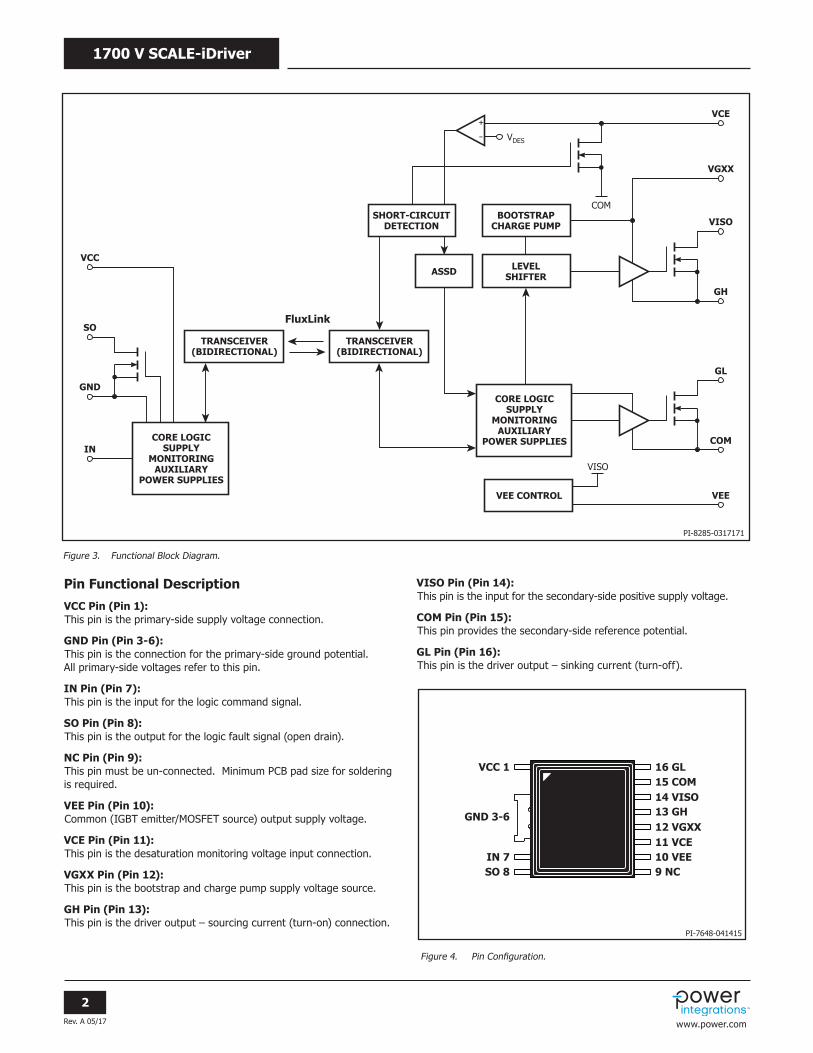
Figure 2. eSOP-R16B Package.
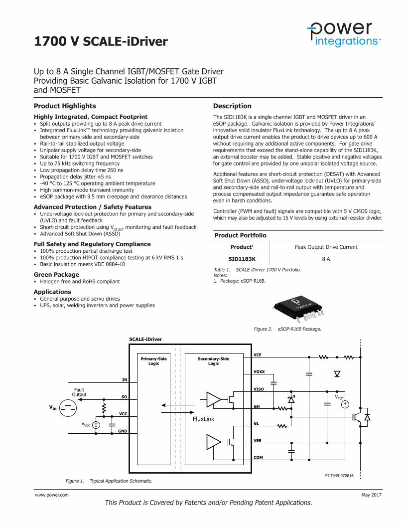
Figure 1. Typical Application Schematic.
DescriptionThe SID1183K is a single channel IGBT and MOSFET driver in an eSOP package. Galvanic isolation is provided by Power Integrations’ innovative solid insulator FluxLink technology. The up to 8 A peak output drive current enables the product to drive devices up to 600 A without requiring any additional active components. For gate drive requirements that exceed the stand-alone capability of the SID1183K, an external booster may be added. Stable positive and negative voltages for gate control are provided by one unipolar isolated voltage source.
Additional features are short-circuit protection (DESAT) with Advanced Soft Shut Down (ASSD), undervoltage lock-out (UVLO) for primary-side and secondary-side and rail-to-rail output with temperature and process compensated output impedance guarantee safe operation even in harsh conditions.
Controller (PWM and fault) signals are compatible with 5 V CMOS logic, which may also be adjusted to 15 V levels by using external resistor divider.
Product Portfolio
Product1 Peak Output Drive Current
SID1183K 8 A
Table 1. SCALE-iDriver 1700 V Portfolio.Notes: 1. Package: eSOP-R16B.
PI-7949-072616
IN
SO
VCC
VIN
GND
FaultOutput
VVCC
SCALE-iDriver
Primary-SideLogic
FluxLink+-
VCE
VISO
VGXX
GH
GL
VEE
COM
Secondary-SideLogic
VTOT+-
Rev. A 05/17
2
1700 V SCALE-iDriver
www.power.com
Pin Functional DescriptionVCC Pin (Pin 1):This pin is the primary-side supply voltage connection.
GND Pin (Pin 3-6):This pin is the connection for the primary-side ground potential. All primary-side voltages refer to this pin.
IN Pin (Pin 7):This pin is the input for the logic command signal.
SO Pin (Pin 8):This pin is the output for the logic fault signal (open drain).
NC Pin (Pin 9):This pin must be un-connected. Minimum PCB pad size for soldering is required.
VEE Pin (Pin 10):Common (IGBT emitter/MOSFET source) output supply voltage.
VCE Pin (Pin 11):This pin is the desaturation monitoring voltage input connection.
VGXX Pin (Pin 12):This pin is the bootstrap and charge pump supply voltage source.
GH Pin (Pin 13):This pin is the driver output – sourcing current (turn-on) connection.
VISO Pin (Pin 14):This pin is the input for the secondary-side positive supply voltage.
COM Pin (Pin 15):This pin provides the secondary-side reference potential.
GL Pin (Pin 16):This pin is the driver output – sinking current (turn-off).
PI-7648-041415
9 NC10 VEE11 VCE12 VGXX13 GH14 VISO15 COM16 GLVCC 1
GND 3-6
IN 7SO 8
Figure 4. Pin Configuration.
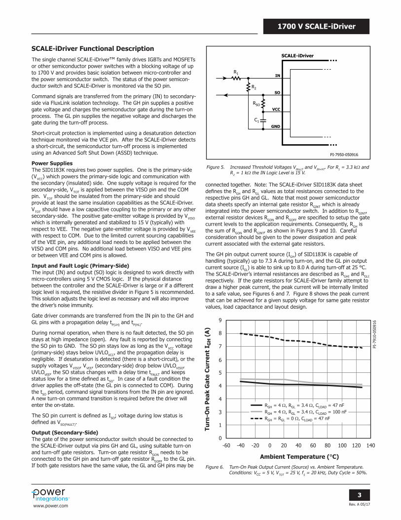
Figure 3. Functional Block Diagram.
PI-8285-0317171
IN
GND
VEE
COM
GL
GH
VISO
VISO
COM
VDES
VGXX
VCE
SO
VCC
FluxLink
TRANSCEIVER(BIDIRECTIONAL)
CORE LOGICSUPPLY
MONITORINGAUXILIARY
POWER SUPPLIES
CORE LOGICSUPPLY
MONITORINGAUXILIARY
POWER SUPPLIES
TRANSCEIVER(BIDIRECTIONAL)
LEVELSHIFTERASSD
VEE CONTROL
BOOTSTRAPCHARGE PUMP
SHORT-CIRCUITDETECTION
+
Rev. A 05/17
3
1700 V SCALE-iDriver
www.power.com
SCALE-iDriver Functional DescriptionThe single channel SCALE-iDriver™ family drives IGBTs and MOSFETs or other semiconductor power switches with a blocking voltage of up to 1700 V and provides basic isolation between micro-controller and the power semiconductor switch. The status of the power semicon-ductor switch and SCALE-iDriver is monitored via the SO pin.
Command signals are transferred from the primary (IN) to secondary- side via FluxLink isolation technology. The GH pin supplies a positive gate voltage and charges the semiconductor gate during the turn-on process. The GL pin supplies the negative voltage and discharges the gate during the turn-off process.
Short-circuit protection is implemented using a desaturation detection technique monitored via the VCE pin. After the SCALE-iDriver detects a short-circuit, the semiconductor turn-off process is implemented using an Advanced Soft Shut Down (ASSD) technique.
Power SuppliesThe SID1183K requires two power supplies. One is the primary-side (VVCC) which powers the primary-side logic and communication with the secondary (insulated) side. One supply voltage is required for the secondary-side, VTOT is applied between the VISO pin and the COM pin. VTOT should be insulated from the primary-side and should provide at least the same insulation capabilities as the SCALE-iDriver. VTOT should have a low capacitive coupling to the primary or any other secondary-side. The positive gate-emitter voltage is provided by VVISO which is internally generated and stabilized to 15 V (typically) with respect to VEE. The negative gate-emitter voltage is provided by VVEE with respect to COM. Due to the limited current sourcing capabilities of the VEE pin, any additional load needs to be applied between the VISO and COM pins. No additional load between VISO and VEE pins or between VEE and COM pins is allowed.
Input and Fault Logic (Primary-Side)The input (IN) and output (SO) logic is designed to work directly with micro-controllers using 5 V CMOS logic. If the physical distance between the controller and the SCALE-iDriver is large or if a different logic level is required, the resistive divider in Figure 5 is recommended. This solution adjusts the logic level as necessary and will also improve the driver’s noise immunity.
Gate driver commands are transferred from the IN pin to the GH and GL pins with a propagation delay tP(LH) and tP(HL).
During normal operation, when there is no fault detected, the SO pin stays at high impedance (open). Any fault is reported by connecting the SO pin to GND. The SO pin stays low as long as the VVCC voltage (primary-side) stays below UVLOVCC, and the propagation delay is negligible. If desaturation is detected (there is a short-circuit), or the supply voltages VVISO, VVEE, (secondary-side) drop below UVLOVISO, UVLOVEE, the SO status changes with a delay time tFAULT and keeps status low for a time defined as tSO. In case of a fault condition the driver applies the off-state (the GL pin is connected to COM). During the tSO period, command signal transitions from the IN pin are ignored. A new turn-on command transition is required before the driver will enter the on-state.
The SO pin current is defined as ISO; voltage during low status is defined as VSO(FAULT).
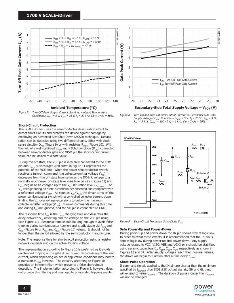
Output (Secondary-Side) The gate of the power semiconductor switch should be connected to the SCALE-iDriver output via pins GH and GL, using suitable turn-on and turn-off gate resistors. Turn-on gate resistor RGON needs to be connected to the GH pin and turn-off gate resistor RGOFF to the GL pin. If both gate resistors have the same value, the GL and GH pins may be
connected together. Note: The SCALE-iDriver SID1183K data sheet defines the RGH and RGL values as total resistances connected to the respective pins GH and GL. Note that most power semiconductor data sheets specify an internal gate resistor RGINT which is already integrated into the power semiconductor switch. In addition to RGINT, external resistor devices RGON and RGOFF are specified to setup the gate current levels to the application requirements. Consequently, RGH is the sum of RGON and RGINT, as shown in Figures 9 and 10. Careful consideration should be given to the power dissipation and peak current associated with the external gate resistors.
The GH pin output current source (IGH) of SID1183K is capable of handling (typically) up to 7.3 A during turn-on, and the GL pin output current source (IGL) is able to sink up to 8.0 A during turn-off at 25 °C. The SCALE-iDriver’s internal resistances are described as RGHI and RGLI respectively. If the gate resistors for SCALE-iDriver family attempt to draw a higher peak current, the peak current will be internally limited to a safe value, see Figures 6 and 7. Figure 8 shows the peak current that can be achieved for a given supply voltage for same gate resistor values, load capacitance and layout design.
Figure 5. Increased Threshold Voltages VIN+LT and VIN+HT. For R1 = 3.3 kW and R2 = 1 kW the IN Logic Level is 15 V.
Figure 6. Turn-On Peak Output Current (Source) vs. Ambient Temperature. Conditions: VCC = 5 V, VTOT = 25 V, fS = 20 kHz, Duty Cycle = 50%.
-60 -40 -20 0 20 40 100 120 1408060
Ambient Temperature (°C)
Turn
-On
Pea
k G
ate
Cur
rent
IG
H (
A)
9
8
6
7
5
4
4
3
0
1
PI-7
910-
0509
16
RGH = 4 Ω, RGL = 3.4 Ω, CLOAD = 47 nFRGH = 4 Ω, RGL = 3.4 Ω, CLOAD = 100 nFRGH = RGL = 0 Ω, CLOAD = 47 nF
PI-7950-050916
SCALE-iDriver
IN
SO
VCC
GND
RSO
R2
R1
C1
Rev. A 05/17
4
1700 V SCALE-iDriver
www.power.com
Figure 9. Short-Circuit Protection Using Diode DVCE.
Figure 7. Turn-Off Peak Output Current (Sink) vs. Ambient Temperature. Conditions: VVCC = 5 V, VTOT = 25 V, fS = 20 kHz, Duty Cycle = 50%. Figure 8. Turn-On and Turn-Off Peak Output Current vs. Secondary-Side Total
Supply Voltage (VTOT). Conditions: VVCC = 5 V, TJ = 25 °C, RGH = 4 W, RGL = 3.4 W, CLOAD = 100 nF, fS = 1 kHz, Duty Cycle = 50%.
-60 -40 -20 0 20 40 100 120 1408060
Ambient Temperature (°C)
Turn
-Off
Pea
k G
ate
Cur
rent
IG
L (A
)
0
-1
-2
-3
-4
-5
-6
-7
-8
-9
-10
PI-7
911-
0428
16
RGH = 4 Ω, RGL = 3.4 Ω, CLOAD = 47 nFRGH = 4 Ω, RGL = 3.4 Ω, CLOAD = 100 nFRGH = RGL = 0 Ω, CLOAD = 47 nF
20 21 22 23 24 25 28 29 302726
Secondary-Side Total Supply Voltage – VTOT (V)
Gat
e P
eak
Cur
rent
(A
)
7
6
5
4
3
2
1
0
PI-7
912-
0428
16
IGH, Turn-On Peak Gate CurrentIGL, Turn-Off Peak Gate Current
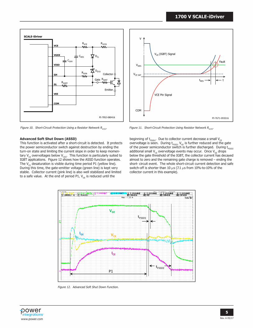
Short-Circuit ProtectionThe SCALE-iDriver uses the semiconductor desaturation effect to detect short-circuits and protects the device against damage by employing an Advanced Soft Shut Down (ASSD) technique. Desatu-ration can be detected using two different circuits, either with diode sense circuitry DVCE (Figure 9) or with resistors RVCEX (Figure 10). With the help of a well stabilized VVISO and a Schottky diode (DSTO) connected between semiconductor gate and VISO pin the short-circuit current value can be limited to a safe value.
During the off-state, the VCE pin is internally connected to the COM pin and CRES is discharged (red curve in Figure 11 represents the potential of the VCE pin). When the power semiconductor switch receives a turn-on command, the collector-emitter voltage (VCE) decreases from the off-state level same as the DC-link voltage to a normally much lower on-state level (see blue curve in Figure 11) and CRES begins to be charged up to the VCE saturation level (VCE SAT). The VCE voltage during on-state is continuously observed and compared with a reference voltage VDES. As soon as VCE>VDES the driver turns off the power semiconductor switch with a controlled collector current slope, limiting the VCE overvoltage excursions to below the maximum collector-emitter voltage (VCES). Turn-on commands during this time and during tSO are ignored, and the SO pin is connected to GND.
The response time tRES is the CRES charging time and describes the delay between VCE asserting and the voltage on the VCE pin rising (see Figure 11). Response time should be long enough to avoid false tripping during semiconductor turn-on and is adjustable via RRES and CRES (Figure 9) or RVCE and CRES (Figure 10) values. It should not be longer than the period allowed by the semiconductor manufacturer.
Note: The response time for short-circuit protection using a resistor network depends also on the actual DC-link voltage.
The implementation according to Figure 10 is preferred as it avoids unintended tripping of the gate driver during zero-crossing of the load current, which depending on actual application conditions may lead to a transient VCESAT increase. The circuitry according to Figure 10 provides an inherent filter, which prevents a false short-circuit detection. The implementation according to Figure 9, however, does not provide this filtering and may lead to unintended tripping events.
Safe Power-Up and Power-DownDuring power-up and power-down the IN pin should stay at logic low. In order to avoid these effects, it is recommended that the IN pin is kept at logic low during power-up and power-down. Any supply voltage related to VCC, VISO, VEE and VGXX pins should be stabilized using ceramic capacitors C1, CS1X, CS2X, CGXX respectively as shown in Figures 13 and 14. After supply voltages reach their nominal values, the driver will begin to function after a time delay tSTART.
Short-Pulse Operation If command signals applied to the IN pin are shorter than the minimum specified by tGE(MIN), then SID1183K output signals, GH and GL pins, will extend to value tGE(MIN). The duration of pulses longer than tGE(MIN) will not be changed.
PI-7951-080416
VCE
VGXX
VISO
GH
RRES
RVCE
DSTO
CGXX
RGOFF
DVCE
Emitter
CollectorRGON
CRES
GL
VEE
COM
SCALE-iDriver
Gate RGINT
Rev. A 05/17
5
1700 V SCALE-iDriver
www.power.com
Figure 10. Short-Circuit Protection Using a Resistor Network RVCEX. Figure 11. Short-Circuit Protection Using Resistor Network RVCEX.
PI-7671-093016
V
VCE (IGBT) Signal
VCE Pin Signal
VDES
VCE SAT
tRES t
Fault
COM
Advanced Soft Shut Down (ASSD)This function is activated after a short-circuit is detected. It protects the power semiconductor switch against destruction by ending the turn-on state and limiting the current slope in order to keep momen-tary VCE overvoltages below VCES. This function is particularly suited to IGBT applications. Figure 12 shows how the ASSD function operates. The VCE desaturation is visible during time period P1 (yellow line). During this time, the gate-emitter voltage (green line) is kept very stable. Collector current (pink line) is also well stabilized and limited to a safe value. At the end of period P1, VGE is reduced until the
Figure 12. Advanced Soft Shut Down Function.
beginning of tFSSD1. Due to collector current decrease a small VCE overvoltage is seen. During tFSSD1 VGE is further reduced and the gate of the power semiconductor switch is further discharged. During tFSSD2 additional small VCE overvoltage events may occur. Once VGE drops below the gate threshold of the IGBT, the collector current has decayed almost to zero and the remaining gate charge is removed ‒ ending the short- circuit event. The whole short-circuit current detection and safe switch-off is shorter than 10 µs (7.1 µs from 10%-to-10% of the collector current in this example).
ICE
VGE
VCEIGE
P1
tFSSD1
tFSSD2
PI-7952-080416
SCALE-iDriver
VCE
VGXX
VISO
GH
RVCEXRVCE
DSTO
CGXX
RGOFF
Emitter
CollectorRGON
CRES
GL
VEE
COM
Gate RGINT
DCL
Rev. A 05/17
6
1700 V SCALE-iDriver
www.power.com
Figure 13. SCALE-iDriver Application Example Using a Resistor Network for Desaturation Detection.
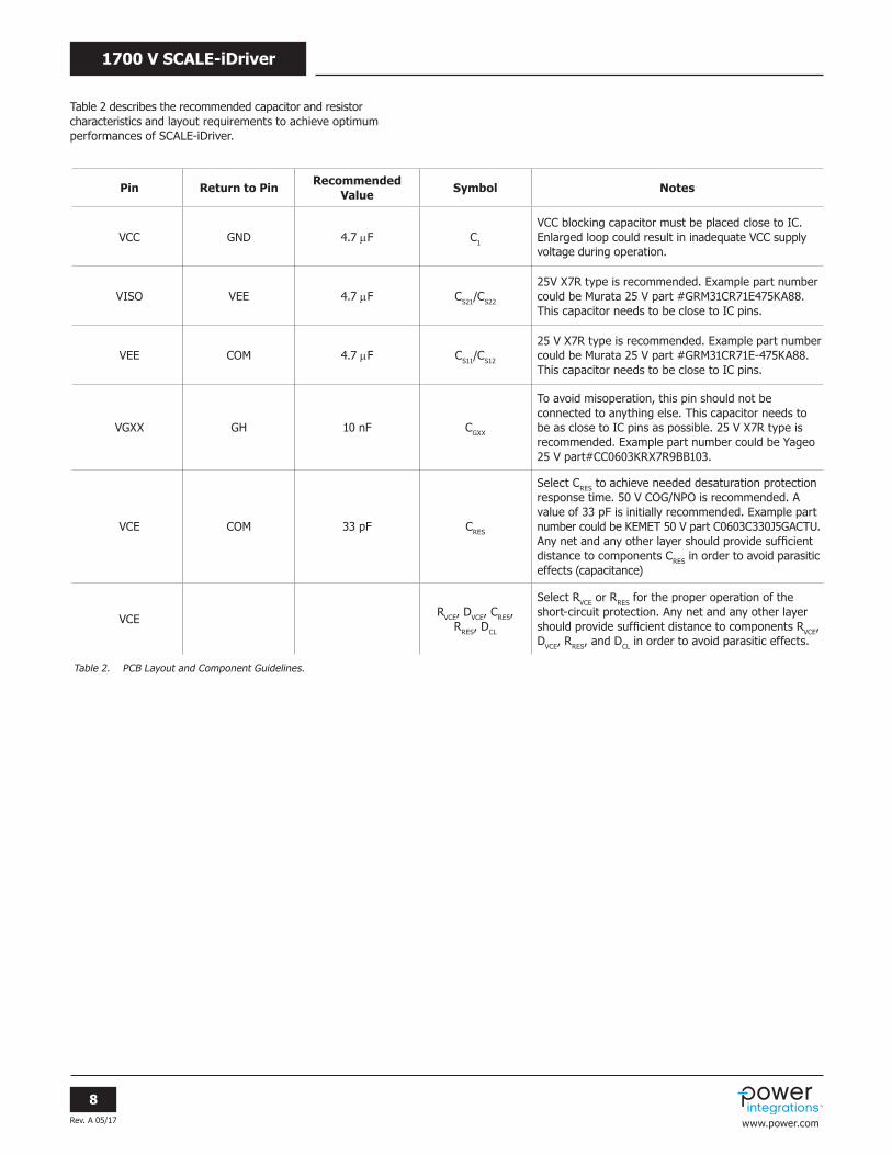
Figure 14. SCALE-iDriver Application Example Using Diodes for Desaturation Detection.
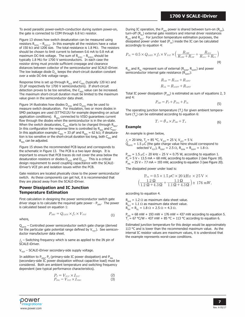
Application Examples and Components SelectionFigures 13 and 14 show the schematic and typical components used for a SID1183K design. In both cases the primary-side supply voltage (VVCC) is connected between VCC and GND pins and supported through a supply bypass ceramic capacitor C1 (4.7 µF typically). If the command signal voltage level is higher than the rated IN pin voltage (in this case 15 V) a resistive voltage divider should be used. Additional capacitor CF and Schmitt trigger IC1 can be used to provide input signal filtering. The SO output has 5 V logic and the RSO is selected so that it does not exceed absolute maximum rated ISO current.
The secondary-side isolated power supply (VTOT) is connected between VISO and COM. The positive voltage rail (VVISO) is supported through 4.7 µF ceramic capacitors CS21 and CS22 connected in parallel. The negative voltage rail (VVEE) is similarly supported through capacitors
CS11 and CS12. The gate charge will vary according to the type of power semiconductor switch that is being driven. Typically, CS11 + CS12 should be at least 3 µF multiplied by the total gate charge of the power semiconductor switch (QGATE) divided by 1 µC. A 10 nF capacitor CGXX is connected between the GH and VGXX pins.
The gate of the power semiconductor switch is connected through resistor RGON to the GH pin and by RGOFF to the GL pin. If the value of RGON is the same as RGOFF the GH pin can be connected to the GL pin and a common gate resistor can be connected to the gate. In each case, proper consideration needs to be given to the power dissipation and temperature performance of the gate resistors.
To ensure gate voltage stabilization and collector current limitation during a short-circuit, the gate is connected to the VISO pin through a Schottky diode DSTO (for example PMEG4010).
PI-8286-031717
CGXX10 nF
CS214.7 µF
CS224.7 µF
CS114.7 µF
CS124.7 µF
RGON
RGOFF
RVCE330 Ω DVCE2 DVCE1
CRES33 pF
RGE6.8 kΩ
RRES62 kΩ
Gate
Emitter
Collector
IN
SO
VCC
GND
CF
SO
RSO4.7 kΩ
R21 kΩ
R13.3 kΩ
VCC
GND
IC174LVC
C14.7 µF
CommandSignal
DSTO
SCALE-iDriver
Primary-SideLogic
Secondary-SideLogic
VCE
VISO
VGXX
GH
GL
VEE
COM
VTOT+-FluxLink
Primary-SideLogic
IN
SO
VCC
GND
CF
SO
RSO4.7 kΩ
R21 kΩ
R13.3 kΩ
VCC
GND
C14.7 µF
CommandSignal
DCLBAS416
PI-8249-032317
CGXX10 nF
CS214.7 µF
CS224.7 µF
CS114.7 µF
CS124.7 µF
RGON
RGOFF
RVCE2-13150 kΩ × 12
CRES33 pF
RGE6.8 kΩ
Gate
Emitter
Collector
DSTO
SCALE-iDriver
Primary-SideLogic
Secondary-SideLogic
RVCE120 kΩ
VCE
VISO
VGXX
GH
GL
VEE
COM
VTOT+-FluxLink
IC174LVC
Rev. A 05/17
7
1700 V SCALE-iDriver
www.power.com
To avoid parasitic power-switch-conduction during system power-on, the gate is connected to COM through 6.8 kW resistor.
Figure 13 shows how switch desaturation can be measured using resistors RVCE2 – RVCE13. In this example all the resistors have a value of 150 kW and 1206 size. The total resistance is 1.8 MW. The resistors should be chosen to limit current to between 0.6 mA to 0.8 mA at maximum DC-link voltage. The sum of RVCE2 – RVCE13 should be typically 1.8 MW for 1700 V semiconductors. In each case the resistor string must provide sufficient creepage and clearance distances between collector of the semiconductor and SCALE-iDriver. The low leakage diode DCL keeps the short-circuit duration constant over a wide DC-link voltage range.
Response time is set up through RVCE and CRES (typically 120 kW and 33 pF respectively for 1700 V semiconductors). If short-circuit detection proves to be too sensitive, the CRES value can be increased. The maximum short-circuit duration must be limited to the maximum value given in the semiconductor data sheet.
Figure 14 illustrates how diodes DVCE1 and DVCE2 may be used to measure switch desaturation. For insulation, two or more diodes in SMD packages are used (STTH212U for example depending on actual application conditions). RRES connected to VISO guarantees current flow through the diodes when the semiconductor is in the on-state. When the switch desaturates, CRES starts to be charged through RRES. In this configuration the response time is controlled by RRES and CRES. In this application example CRES = 33 pF and RRES = 62 kW; if desatura-tion is too sensitive or the short-circuit duration too long, both CRES and RRES can be adjusted.
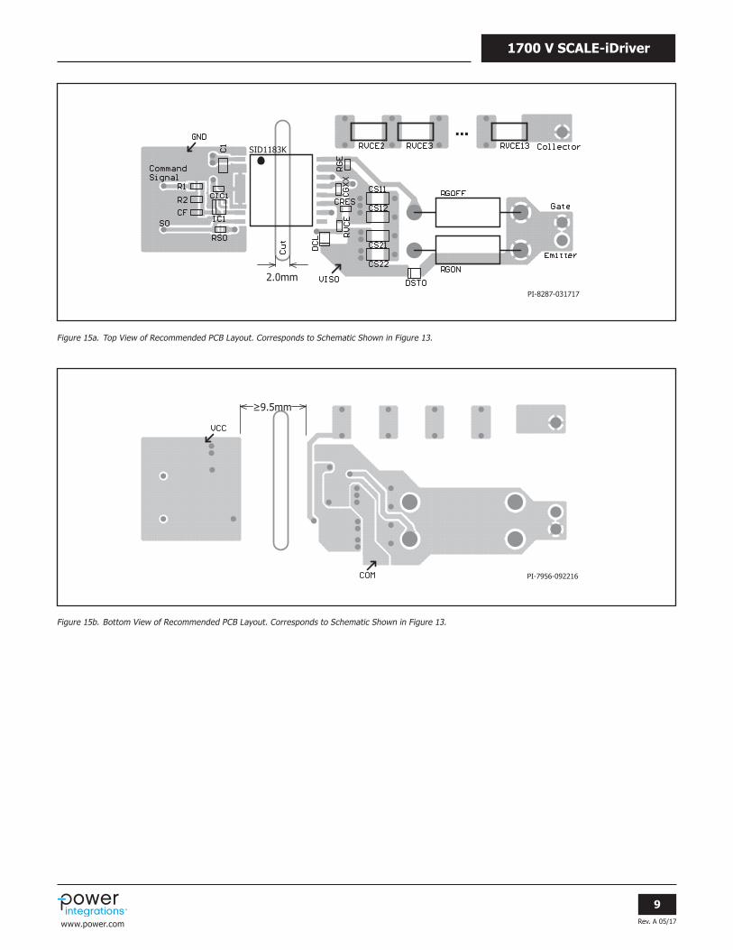
Figure 15 shows the recommended PCB layout and corresponds to the schematic in Figure 13. The PCB is a two layer design. It is important to ensure that PCB traces do not cover the area below the desaturation resistors or diodes DVCE1 and DVCE2. This is a critical design requirement to avoid coupling capacitance with the SCALE-iDriver’s VCE pin and isolation issues within the PCB.
Gate resistors are located physically close to the power semiconductor switch. As these components can get hot, it is recommended that they are placed away from the SCALE-iDriver.
Power Dissipation and IC Junction Temperature EstimationFirst calculation in designing the power semiconductor switch gate driver stage is to calculate the required gate power - PDRV. The power is calculated based on equation 1:
P Q f VDRV GATE S TOT# #= (1)where,
QGATE – Controlled power semiconductor switch gate charge (derived for the particular gate potential range defined by VTOT). See semicon-ductor manufacturer data sheet.
ƒS – Switching frequency which is same as applied to the IN pin of SCALE-iDriver.
VTOT – SCALE-iDriver secondary-side supply voltage.
In addition to PDRV, PP (primary-side IC power dissipation) and PSNL (secondary-side IC power dissipation without capacitive load) must be considered. Both are ambient temperature and switching frequency dependent (see typical performance characteristics).
P V IVCC VCCP #= (2) P V ITOT VISOSNL #= (3)
During IC operation, the PDRV power is shared between turn-on (RGH), turn-off (RGL) external gate resistors and internal driver resistances RGHI and RGLI. For junction temperature estimation purposes, the dissipated power under load (POL) inside the IC can be calculated accordingly to equation 4:
. V R RR
R RR
P Q f0 5OL GATE S TOTGHI GH
GHI
GL I G L
GL I# ## #= + + +b l
(4)
RGH and RGL represent sum of external (RGON, RGOFF) and power semiconductor internal gate resistance (RGINT):
R R R
R R R
GH GON GINT
GL GOFF GINT
= +
= +
Total IC power dissipation (PDIS) is estimated as sum of equations 2, 3 and 4:
P P P PDIS OLP SNL= + + (5)
The operating junction temperature (TJ) for given ambient tempera-ture (TA) can be estimated according to equation 6:
T P TJ JA DIS A#i= + (6)Example
An example is given below,
ƒS = 20 kHz, TA = 85 °C, VTOT = 25 V, VVCC = 5 V. QGATE = 1.5 µC (the gate charge value here should correspond to selected VTOT), RGINT = 2.5 W, RGON = RGOFF = 1.8 W.
PDRV = 1.5 µC × 20 kHz × 25 V = 0.75 W, according to equation 1.PP = 5 V × 13.5 mA = 68 mW, according to equation 2 (see Figure 18).PSNL = 25 V × 7.7 mA = 193 mW, according to equation 3 (see Figure 20).
The dissipated power under load is:
. .
. ..
. .. mW
P 0 5 1 5 C 20 kHz 25V
1 2 4 31 2
1 1 4 31 1 176
OL # # # #
≅
n
X XX
X XX
=
+ + +b l ,
according to equation 4.
RGHI = 1.2 W as maximum data sheet value.RGLI = 1.1 W as maximum data sheet value.RGH = RGL = 1.8 W + 2.5 W = 4.3 W.
PDIS = 68 mW + 193 mW + 176 mW = 437 mW according to equation 5.TJ = 67 °C/W × 437 mW + 85 °C = 113 °C according to equation 6.
Estimated junction temperature for this design would be approximately 113 °C and is lower than the recommended maximum value. As the internal IC resistor values are maximum values, it is understood that the example represents worst-case conditions.
Rev. A 05/17
8
1700 V SCALE-iDriver
www.power.com
Table 2 describes the recommended capacitor and resistor characteristics and layout requirements to achieve optimum performances of SCALE-iDriver.
Pin Return to Pin RecommendedValue Symbol Notes
VCC GND 4.7 µF C1
VCC blocking capacitor must be placed close to IC. Enlarged loop could result in inadequate VCC supply voltage during operation.
VISO VEE 4.7 µF CS21/CS22
25V X7R type is recommended. Example part numbercould be Murata 25 V part #GRM31CR71E475KA88.This capacitor needs to be close to IC pins.
VEE COM 4.7 µF CS11/CS12
25 V X7R type is recommended. Example part number could be Murata 25 V part #GRM31CR71E-475KA88. This capacitor needs to be close to IC pins.
VGXX GH 10 nF CGXX
To avoid misoperation, this pin should not be connected to anything else. This capacitor needs to be as close to IC pins as possible. 25 V X7R type is recommended. Example part number could be Yageo 25 V part#CC0603KRX7R9BB103.
VCE COM 33 pF CRES
Select CRES to achieve needed desaturation protection response time. 50 V COG/NPO is recommended. A value of 33 pF is initially recommended. Example part number could be KEMET 50 V part C0603C330J5GACTU. Any net and any other layer should provide sufficient distance to components CRES in order to avoid parasitic effects (capacitance)
VCE RVCE, DVCE, CRES, RRES, DCL
Select RVCE or RRES for the proper operation of the short-circuit protection. Any net and any other layer should provide sufficient distance to components RVCE, DVCE, RRES, and DCL in order to avoid parasitic effects.
Table 2. PCB Layout and Component Guidelines.
Rev. A 05/17
9
1700 V SCALE-iDriver
www.power.com
Figure 15b. Bottom View of Recommended PCB Layout. Corresponds to Schematic Shown in Figure 13.
Figure 15a. Top View of Recommended PCB Layout. Corresponds to Schematic Shown in Figure 13.
PI-7956-092216
PI-8287-031717
SID1183K
Rev. A 05/17
10
1700 V SCALE-iDriver
www.power.com
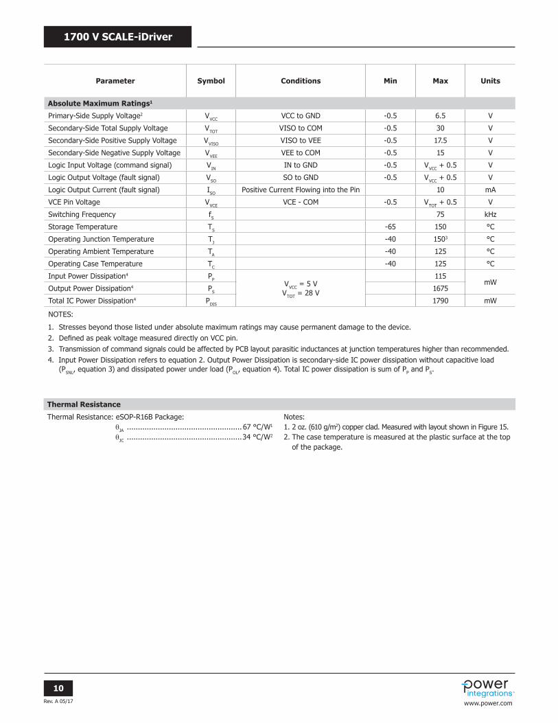
Thermal Resistance
Thermal Resistance: eSOP-R16B Package: qJA .................................................... 67 °C/W1 qJC ....................................................34 °C/W2
Notes:1. 2 oz. (610 g/m2) copper clad. Measured with layout shown in Figure 15.2. The case temperature is measured at the plastic surface at the top
of the package.
Parameter Symbol Conditions Min Max Units
Absolute Maximum Ratings1
Primary-Side Supply Voltage2 VVCC VCC to GND -0.5 6.5 V
Secondary-Side Total Supply Voltage VTOT VISO to COM -0.5 30 V
Secondary-Side Positive Supply Voltage VVISO VISO to VEE -0.5 17.5 V
Secondary-Side Negative Supply Voltage VVEE VEE to COM -0.5 15 V
Logic Input Voltage (command signal) VIN IN to GND -0.5 VVCC + 0.5 V
Logic Output Voltage (fault signal) VSO SO to GND -0.5 VVCC + 0.5 V
Logic Output Current (fault signal) ISO Positive Current Flowing into the Pin 10 mA
VCE Pin Voltage VVCE VCE - COM -0.5 VTOT + 0.5 V
Switching Frequency fS 75 kHz
Storage Temperature TS -65 150 °C
Operating Junction Temperature TJ -40 1503 °C
Operating Ambient Temperature TA -40 125 °C
Operating Case Temperature TC -40 125 °C
Input Power Dissipation4 PPVVCC = 5 VVTOT = 28 V
115mW
Output Power Dissipation4 PS 1675
Total IC Power Dissipation4 PDIS 1790 mW
NOTES:
1. Stresses beyond those listed under absolute maximum ratings may cause permanent damage to the device. 2. Defined as peak voltage measured directly on VCC pin. 3. Transmission of command signals could be affected by PCB layout parasitic inductances at junction temperatures higher than recommended.4. Input Power Dissipation refers to equation 2. Output Power Dissipation is secondary-side IC power dissipation without capacitive load
(PSNL, equation 3) and dissipated power under load (POL, equation 4). Total IC power dissipation is sum of PP and PS.
Rev. A 05/17
11
1700 V SCALE-iDriver
www.power.com
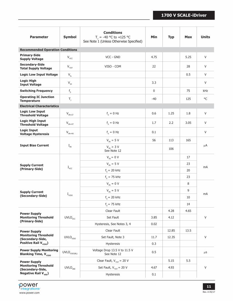
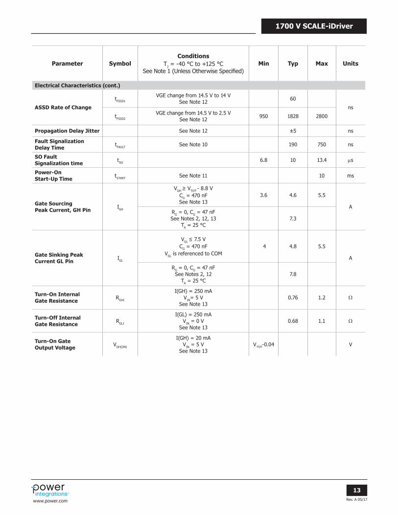
Parameter SymbolConditions
TJ = -40 °C to +125 °C See Note 1 (Unless Otherwise Specified)
Min Typ Max Units
Recommended Operation Conditions
Primary-Side Supply Voltage VVCC VCC - GND 4.75 5.25 V
Secondary-Side Total Supply Voltage VTOT VISO - COM 22 28 V
Logic Low Input Voltage VIL 0.5 V
Logic High Input Voltage VIH 3.3 V
Switching Frequency fS 0 75 kHz
Operating IC Junction Temperature TJ -40 125 °C
Electrical Characteristics
Logic Low Input Threshold Voltage VIN+LT fS = 0 Hz 0.6 1.25 1.8 V
Logic High Input Threshold Voltage VIN+HT fS = 0 Hz 1.7 2.2 3.05 V
Logic Input Voltage Hysteresis VIN+HS fS = 0 Hz 0.1 V
Input Bias Current IIN
VIN = 5 V 56 113 165
µAVIN > 3 VSee Note 12 106
Supply Current (Primary-Side) IVCC
VIN = 0 V 17
mAVIN = 5 V 23
fS = 20 kHz 20
fS = 75 kHz 23
Supply Current (Secondary-Side) IVISO
VIN = 0 V 8
mAVIN = 5 V 9
fS = 20 kHz 10
fS = 75 kHz 14
Power Supply Monitoring Threshold (Primary-Side)
UVLOVCC
Clear Fault 4.28 4.65
VSet Fault 3.85 4.12
Hysteresis, See Notes 3, 4 0.02
Power Supply Monitoring Threshold (Secondary-Side, Positive Rail VVISO)
UVLOVISO
Clear Fault 12.85 13.5
VSet Fault, Note 3 11.7 12.35
Hysteresis 0.3
Power Supply Monitoring Blanking Time, VVISO
UVLOVISO(BL)
Voltage Drop 13.5 V to 11.5 VSee Note 12 0.5 µs
Power Supply Monitoring Threshold (Secondary-Side, Negative Rail VVEE)
UVLOVEE
Clear Fault, VTOT = 20 V 5.15 5.5
VSet Fault, VTOT = 20 V 4.67 4.93
Hysteresis 0.1
Rev. A 05/17
12
1700 V SCALE-iDriver
www.power.com
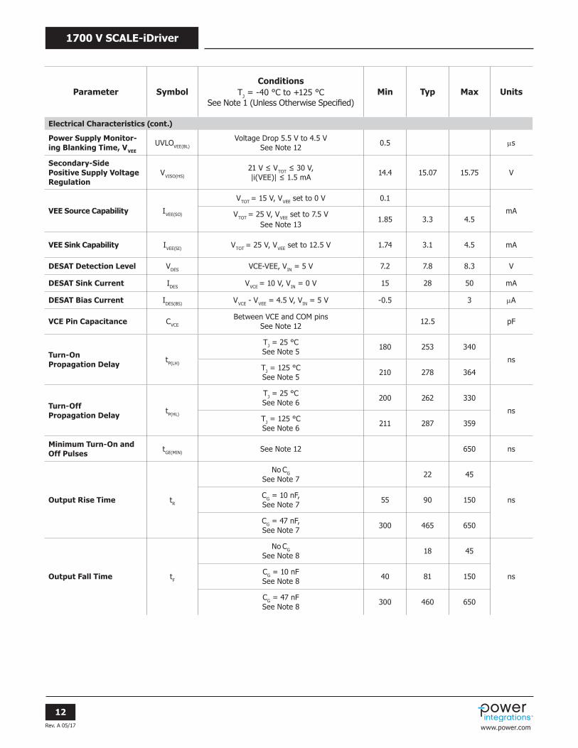
Parameter SymbolConditions
TJ = -40 °C to +125 °C See Note 1 (Unless Otherwise Specified)
Min Typ Max Units
Electrical Characteristics (cont.)
Power Supply Monitor-ing Blanking Time, VVEE
UVLOVEE(BL)
Voltage Drop 5.5 V to 4.5 VSee Note 12 0.5 µs
Secondary-Side Positive Supply Voltage Regulation
VVISO(HS)
21 V ≤ VTOT ≤ 30 V, |i(VEE)| ≤ 1.5 mA 14.4 15.07 15.75 V
VEE Source Capability IVEE(SO)
VTOT = 15 V, VVEE set to 0 V 0.1
mAVTOT = 25 V, VVEE set to 7.5 VSee Note 13
1.85 3.3 4.5
VEE Sink Capability IVEE(SI) VTOT = 25 V, VVEE set to 12.5 V 1.74 3.1 4.5 mA
DESAT Detection Level VDES VCE-VEE, VIN = 5 V 7.2 7.8 8.3 V
DESAT Sink Current IDES VVCE = 10 V, VIN = 0 V 15 28 50 mA
DESAT Bias Current IDES(BS) VVCE - VVEE = 4.5 V, VIN = 5 V -0.5 3 µA
VCE Pin Capacitance CVCE
Between VCE and COM pinsSee Note 12 12.5 pF
Turn-On Propagation Delay tP(LH)
TJ = 25 °CSee Note 5 180 253 340
nsTJ = 125 °CSee Note 5 210 278 364
Turn-Off Propagation Delay tP(HL)
TJ = 25 °CSee Note 6 200 262 330
nsTJ = 125 °CSee Note 6 211 287 359
Minimum Turn-On and Off Pulses tGE(MIN) See Note 12 650 ns
Output Rise Time tR
No CG
See Note 7 22 45
nsCG = 10 nF, See Note 7 55 90 150
CG = 47 nF, See Note 7 300 465 650
Output Fall Time tF
No CG
See Note 8 18 45
nsCG = 10 nFSee Note 8 40 81 150
CG = 47 nFSee Note 8 300 460 650
Rev. A 05/17
13
1700 V SCALE-iDriver
www.power.com
Parameter SymbolConditions
TJ = -40 °C to +125 °C See Note 1 (Unless Otherwise Specified)
Min Typ Max Units
Electrical Characteristics (cont.)
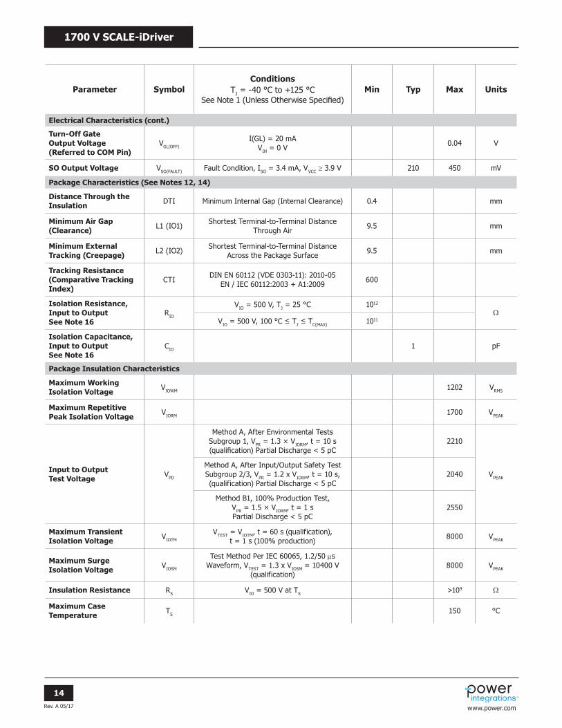
ASSD Rate of Change
tFSSD1
VGE change from 14.5 V to 14 VSee Note 12 60
ns
tFSSD2
VGE change from 14.5 V to 2.5 VSee Note 12 950 1828 2800
Propagation Delay Jitter See Note 12 ±5 ns
Fault Signalization Delay Time tFAULT See Note 10 190 750 ns
SO Fault Signalization time tSO 6.8 10 13.4 µs
Power-On Start-Up Time tSTART See Note 11 10 ms
Gate Sourcing Peak Current, GH Pin IGH
VGH ≥ VTOT - 8.8 V CG = 470 nFSee Note 13
3.6 4.6 5.5
ARG = 0, CG = 47 nF See Notes 2, 12, 13
TA = 25 °C7.3
Gate Sinking Peak Current GL Pin IGL
VGL ≤ 7.5 VCG = 470 nF
VGL is referenced to COM 4 4.8 5.5
A
RG = 0, CG = 47 nFSee Notes 2, 12
TA = 25 °C7.8
Turn-On Internal Gate Resistance RGHI
I(GH) = 250 mAVIN= 5 V
See Note 130.76 1.2 W
Turn-Off Internal Gate Resistance RGLI
I(GL) = 250 mAVIN = 0 V
See Note 130.68 1.1 W
Turn-On Gate Output Voltage VGH(ON)
I(GH) = 20 mAVIN = 5 V
See Note 13VTOT-0.04 V
Rev. A 05/17
14
1700 V SCALE-iDriver
www.power.com
Package Insulation Characteristics
Maximum Working Isolation Voltage VIOWM 1202 VRMS
Maximum Repetitive Peak Isolation Voltage VIORM 1700 VPEAK
Input to Output Test Voltage VPD
Method A, After Environmental Tests Subgroup 1, VPR = 1.3 × VIORM, t = 10 s (qualification) Partial Discharge < 5 pC
2210
VPEAK
Method A, After Input/Output Safety Test Subgroup 2/3, VPR = 1.2 x VIORM, t = 10 s, (qualification) Partial Discharge < 5 pC
2040
Method B1, 100% Production Test,VPR = 1.5 × VIORM, t = 1 sPartial Discharge < 5 pC
2550
Maximum Transient Isolation Voltage VIOTM
VTEST = VIOTM, t = 60 s (qualification), t = 1 s (100% production) 8000 VPEAK
Maximum Surge Isolation Voltage VIOSM
Test Method Per IEC 60065, 1.2/50 µs Waveform, VTEST = 1.3 x VIOSM = 10400 V
(qualification)8000 VPEAK
Insulation Resistance RS VIO = 500 V at TS >109 W
Maximum Case Temperature TS 150 °C
Parameter SymbolConditions
TJ = -40 °C to +125 °C See Note 1 (Unless Otherwise Specified)
Min Typ Max Units
Electrical Characteristics (cont.)
Turn-Off Gate Output Voltage (Referred to COM Pin)
VGL(OFF)
I(GL) = 20 mA VIN = 0 V 0.04 V
SO Output Voltage VSO(FAULT) Fault Condition, ISO = 3.4 mA, VVCC ≥ 3.9 V 210 450 mV
Package Characteristics (See Notes 12, 14)
Distance Through the Insulation DTI Minimum Internal Gap (Internal Clearance) 0.4 mm
Minimum Air Gap (Clearance) L1 (IO1) Shortest Terminal-to-Terminal Distance
Through Air 9.5 mm
Minimum External Tracking (Creepage) L2 (IO2) Shortest Terminal-to-Terminal Distance
Across the Package Surface 9.5 mm
Tracking Resistance (Comparative Tracking Index)
CTI DIN EN 60112 (VDE 0303-11): 2010-05EN / IEC 60112:2003 + A1:2009 600
Isolation Resistance, Input to Output See Note 16
RIO
VIO = 500 V, TJ = 25 °C 1012
WVIO = 500 V, 100 °C ≤ TJ ≤ TC(MAX) 1011
Isolation Capacitance, Input to OutputSee Note 16
CIO 1 pF
Rev. A 05/17
15
1700 V SCALE-iDriver
www.power.com
Parameter SymbolConditions
TJ = -40 °C to +125 °C See Note 1 (Unless Otherwise Specified)
Min Typ Max Units
Package Insulation Characteristics (cont.)
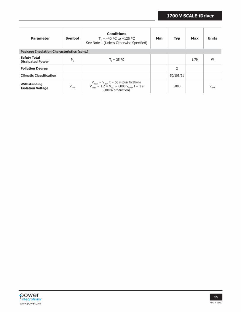
Safety Total Dissipated Power PS TJ = 25 °C 1.79 W
Pollution Degree 2
Climatic Classification 50/105/21
Withstanding Isolation Voltage VISO
VTEST = VISO, t = 60 s (qualification),VTEST = 1.2 × VISO = 6000 VRMS, t = 1 s
(100% production)5000 VRMS
Rev. A 05/17
16
1700 V SCALE-iDriver
www.power.com
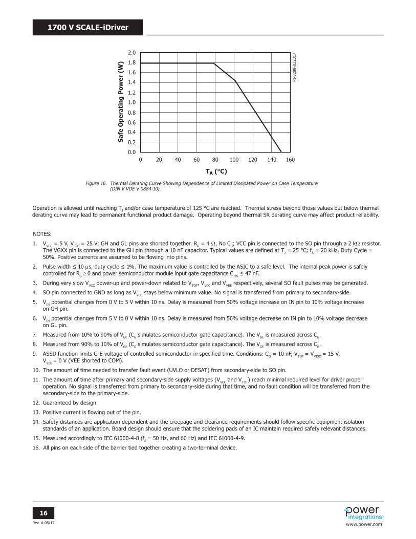
Figure 16. Thermal Derating Curve Showing Dependence of Limited Dissipated Power on Case Temperature (DIN V VDE V 0884-10).
Operation is allowed until reaching TJ and/or case temperature of 125 °C are reached. Thermal stress beyond those values but below thermal derating curve may lead to permanent functional product damage. Operating beyond thermal SR derating curve may affect product reliability.
NOTES:
1. VVCC = 5 V, VTOT = 25 V; GH and GL pins are shorted together. RG = 4 W, No CG; VCC pin is connected to the SO pin through a 2 kW resistor. The VGXX pin is connected to the GH pin through a 10 nF capacitor. Typical values are defined at TJ = 25 °C; fS = 20 kHz, Duty Cycle = 50%. Positive currents are assumed to be flowing into pins.
2. Pulse width ≤ 10 µs, duty cycle ≤ 1%. The maximum value is controlled by the ASIC to a safe level. The internal peak power is safely controlled for RG ≥ 0 and power semiconductor module input gate capacitance CIES ≤ 47 nF.
3. During very slow VVCC power-up and power-down related to VTOT, VVCC and VVEE respectively, several SO fault pulses may be generated.
4. SO pin connected to GND as long as VVCC stays below minimum value. No signal is transferred from primary to secondary-side.
5. VIN potential changes from 0 V to 5 V within 10 ns. Delay is measured from 50% voltage increase on IN pin to 10% voltage increase on GH pin.
6. VIN potential changes from 5 V to 0 V within 10 ns. Delay is measured from 50% voltage decrease on IN pin to 10% voltage decrease on GL pin.
7. Measured from 10% to 90% of VGE (CG simulates semiconductor gate capacitance). The VGE is measured across CG.
8. Measured from 90% to 10% of VGE (CG simulates semiconductor gate capacitance). The VGE is measured across CG.
9. ASSD function limits G-E voltage of controlled semiconductor in specified time. Conditions: CG = 10 nF, VTOT = VVISO = 15 V, VVEE = 0 V (VEE shorted to COM).
10. The amount of time needed to transfer fault event (UVLO or DESAT) from secondary-side to SO pin.
11. The amount of time after primary and secondary-side supply voltages (VVCC and VTOT) reach minimal required level for driver proper operation. No signal is transferred from primary to secondary-side during that time, and no fault condition will be transferred from the secondary-side to the primary-side.
12. Guaranteed by design.
13. Positive current is flowing out of the pin.
14. Safety distances are application dependent and the creepage and clearance requirements should follow specific equipment isolation standards of an application. Board design should ensure that the soldering pads of an IC maintain required safety relevant distances.
15. Measured accordingly to IEC 61000-4-8 (fS = 50 Hz, and 60 Hz) and IEC 61000-4-9.
16. All pins on each side of the barrier tied together creating a two-terminal device.
0 20 40 60 80 100 120 140 160
TA (°C)
Safe
Ope
rati
ng P
ower
(W
)
2.0
1.8
1.4
1.6
1.2
0.6
0.8
1.0
0.4
0.0
0.2
PI-8
288-
0323
17
Rev. A 05/17
17
1700 V SCALE-iDriver
www.power.com
Typical Performance Characteristics
-60 -40 -20 0 20 40 100 120 1408060
Ambient Temperature (°C)
Inpu
t B
ias
Cur
rent
IIN
(µ
A)
117
116
114
115
113
110
111
112
109
108
PI-7
913-
1107
16
-60 -40 -20 0 20 40 100 120 1408060
Ambient Temperature (°C)
Supp
ly C
urre
nt I
VC
C (
mA
)
25
15
20
10
5
0
PI-8
289-
0323
17
IN = 0 V DCIN = 5 V DCfSW = 20 kHzfSW = 75 kHz
0 10 3020 40 50 60 70 80
Switching Frequency – fS (kHz)
Supp
ly C
urre
nt I
VC
C (
mA
)
25
20
10
15
5
0
PI-8
290-
0324
17
-60 -40 0 20-20 40 100 120 1408060
Ambient Temperature (°C)
Supp
ly C
urre
nt I
VIS
O (
mA
)11.0
10.5
9.5
9.0
10.0
7.5
8.0
8.5
7.0
6.5
6.0
PI-7
915-
1107
16
IN = 0 V DCIN = 5 V DCfS = 20 kHzfS = 75 kHz
0 10 20 30 40 70 8050 60
Switching Frequency – fS (kHz)
Supp
ly C
urre
nt I
VIS
O (
mA
)
12
8
10
6
4
2
0
PI-8
293-
0327
17
VTOT = 22 VVTOT = 25 VVTOT = 28 V
Figure 17. Input Bias Current vs. Ambient Temperature. Conditions: VVCC = 5 V, VIN = 5 V, VTOT = 25 V.
Figure 19. Supply Current Primary-Side IVCC vs. Switching Frequency. Conditions: VVCC = 5 V, VTOT = 25 V, TJ= 25 °C, No-Load.
Figure 20. Supply Current Secondary-Side IVISO vs. Ambient Temperature. Conditions: VVCC = 5 V, VTOT = 25 V, No-Load.
Figure 18. Supply Current Primary-Side IVCC vs. Ambient Temperature. Conditions: VVCC = 5 V, VTOT = 25 V, No-Load.
Figure 21. Supply Current Secondary-Side IVISO vs. Switching Frequency. Conditions: VVCC = 5 V, No-Load.
-60 -40 -20 0 20 40 100 120 1408060
Ambient Temperature (°C)
Pro
paga
tion
Del
ay (
ns)
350
200
250
300
150
100
50
0
PI-7
918-
0414
16
tP(HL), Turn-On DelaytP(LH), Turn-Off Delay
Figure 22. Propagation Delay Time vs. Ambient Temperature. Conditions: VVCC = 5 V, VTOT = 25 V, fS = 20 kHz, CLOAD = 2.2 nF.
Rev. A 05/17
18
1700 V SCALE-iDriver
www.power.com
Typical Performance Characteristics
Figure 25. Power Supply Monitoring Hysteresis UVLOVCC vs. Ambient Temperature. Conditions: VTOT = 25 V.
Figure 24. Power Supply Monitoring UVLOVCC vs. Ambient Temperature. Conditions: VTOT = 25 V.
Figure 23. SO Fault Signalization Time vs. Ambient Temperature. Conditions: VVCC = 5 V, VTOT = 25 V, RSO = 4.7 kW.
Figure 26. Power Supply Monitoring Positive Rail UVLOVISO vs. Ambient Temperature. Conditions: VVCC = 5 V.
Figure 27 Power Supply Monitoring Positive Rail Hysteresis UVLOVISO vs. Ambient Temperature. Conditions: VVCC = 5 V.
-60 -40 -20 0 20 40 100 120 1408060
Ambient Temperature (°C)
SO F
ault
Sig
naliz
atio
n Ti
me
– t S
O (µ
s)
12
6
8
10
4
2
0
PI-7
919-
1107
16
-60 -40 -20 0 20 40 100 120 1408060
Ambient Temperature (°C)
Pri
mar
y-Si
de P
ower
Sup
ply
Mon
itor
ing
UV
LOV
CC (
V)
4.5
2.5
3.0
3.5
4.0
1.5
2.0
0.5
1.0
0.0
PI-7
921-
0401
16
Clear FaultSet Fault
-60 -40 -20 0 20 40 100 120 1408060
Ambient Temperature (°C)
Pri
mar
y-Si
de P
ower
Sup
ply
Mon
itor
ing
Hys
tere
sis
UV
LOV
CC (
mV
)
200
120
140
160
180
80
100
20
40
60
0
PI-7
922-
0517
16
-60 -40 -20 0 20 40 100 120 1408060
Ambient Temperature (°C)
Seco
ndar
y-Si
de P
ower
Sup
ply
Mon
itor
ing
Pos
itiv
e R
ail U
VLO
VIS
O (
V)
14
8
10
12
4
6
2
0
PI-7
924-
0401
16
Clear FaultSet Fault
-60 -40 -20 0 20 40 100 120 1408060
Ambient Temperature (°C)
Seco
ndar
y-Si
de P
ower
Sup
ply
Mon
itor
ing
Pos
itiv
e R
ail H
yste
resi
s U
VLO
VIS
O (
mV
)
800
500
600
700
400
100
200
300
0
PI-7
923-
0401
16
Figure 28. Power Supply Monitoring Negative Rail UVLOVEE vs. Ambient Temperature. Conditions: VVCC = 5 V.
-60 -40 -20 0 20 40 100 120 1408060
Ambient Temperature (°C)
Seco
ndar
y-Si
de P
ower
Sup
ply
Mon
itor
ing
Neg
ativ
e R
ail U
VLO
VEE
(V
)
6
4
5
2
3
1
0
PI-7
926-
0401
16Clear FaultSet Fault
Rev. A 05/17
19
1700 V SCALE-iDriver
www.power.com
Figure 32. VEE Sink Capability IVEE(SI) vs. Ambient Temperature and VVISO. Conditions: VVCC = 5 V, fS = 20 kHz, Duty Cycle = 50%.
Figure 31. VEE Source Capability IVEE(SO) vs. Ambient Temperature and VVISO. Conditions: VVCC = 5 V, fS = 20 kHz, Duty Cycle = 50%.
Typical Performance Characteristics
Figure 30. Desaturation Detection Level VDES vs. Ambient Temperature. Conditions: VVCC = 5 V.
Figure 29. Power Supply Monitoring Negative Rail Hysteresis UVLOVEE vs. Ambient Temperature. Conditions: VVCC = 5 V.
-60 -40 -20 0 20 40 100 120 1408060
Ambient Temperature (°C)
Seco
ndar
y-Si
de P
ower
Sup
ply
Mon
itor
ing
Neg
ativ
e R
ail H
yste
resi
s U
VLO
VEE
(m
V)
300
200
250
150
50
100
0
PI-7
925-
1107
16
-60 -40 -20 0 20 40 100 120 1408060
Ambient Temperature (°C)
DES
AT
Det
ecti
on L
evel
VD
ES (
V) 9.0
7.5
8.0
8.5
6.5
7.0
5.5
6.0
5.0
PI-7
927-
0401
16
VTOT = 22 VVTOT = 25 VVTOT = 28 V
-60 -40 -20 0 20 40 100 120 1408060
Ambient Temperature (°C)
I VEE
(SI)
Sin
k C
apab
ility
(m
A)
3.50
3.30
3.25
3.35
3.45
3.40
3.20
3.05
3.15
3.10
3.00
PI-794
8-05
0416
VTOT = 22 V and VVISO = 12.5 VVTOT = 25 V and VVISO = 12.5 VVTOT = 28 V and VVISO = 12.5 V
-60 -40 -20 0 20 40 100 120 1408060
Ambient Temperature (°C)
I VEE
(SO
) So
urce
Cap
abili
ty (
mA
) 3.60
3.40
3.35
3.45
3.55
3.50
3.30
3.15
3.20
3.25
3.10
PI-7
928-
1107
16
VTOT = 22 V and VVISO = 17.5 VVTOT = 25 V and VVISO = 17.5 VVTOT = 28 V and VVISO = 17.5 V
Rev. A 05/17
20
1700 V SCALE-iDriver
www.power.com
PI-6995-051716POD-eSOP-R16B Rev B
Notes:1. Dimensioning and tolerancing per ASME Y14.5M-1994. 2. Dimensions noted are determined at the outermost extremes of the plastic body exclusive of mold flash, tie bar burrs, gate burrs, and inter-lead flash, but including any mismatch between the top and bottom of the plastic body. Maximum mold protrusion is 0.007 [0.18] per side.3. Dimensions noted are inclusive of plating thickness.
4. Does not include inter-lead flash or protrusions.5. Controlling dimensions in inches [mm].6. Datums A and B to be determined in Datum H.7. Exposed metal at the plastic package body outline/surface between leads 6 and 7, connected internally to wide lead 3/4/5/6.
0.356 [9.04]Ref.
0.306 [7.77] Ref.
0.080 [2.03] Ref.
0.050 [1.27]
0.464 [11.79]
0.010 [0.25]
0.400 [10.16]
0.350 [8.89]
Pin #1 I.D.(Laser Marked)
16 9 9 10 11 12 13 14 15 16
1 8 8 7 6 5 4 3 1
2
2
0.045 [1.14] Ref.0.158 [4.01]0.152 [3.86]
0.040 [1.02]0.028 [0.71]
0.032 [0.81]0.029 [0.74]
0.012 [0.30]0.004 [0.10]
0.049 [1.23]0.046 [1.16]
0.092 [2.34]0.086 [2.18]
Detail A
0.105 [2.67]0.093 [2.36]
Gauge Plane
Seating Plane
43
SIDE VIEW
TOP VIEW BOTTOM VIEW
DETAIL A
END VIEW
0.059 [1.50]Ref. Typ.
0.010 [0.25] Ref.
0.019 [0.48]Ref.
0.022 [0.56] Ref.0.020 [0.51]
Ref.
0.028 [0.71]Ref.
0.057 [1.45] Ref.
0° - 8°
0.059 [1.50]Ref. Typ.
0.010 [0.24]Ref.
13X0.023 [0.58]0.018 [0.46]0.010 [0.25] M C A B
43
0.004 [0.10] 2X
12X
C B
0.004 [0.10] 12 LeadsSeating Plane to
Molded BumpsStandoff
SeatingPlane
C
0.004 [0.10] 2X C A
0.006 [0.15] 8 Lead Tips
C
0.006 [0.15] 4 Lead Tips
CB
C
H
A
0.016 [0.41]0.011 [0.28]
C
7
3
.028 [0.71]
.070 [1.78] .460 [11.68]
.162 [4.11]
.165 [4.19]
.300 [7.62]INCH [mm]
.350 [8.89]
.050 [1.27]
eSOP-R16B
ReferenceSolder PadDimensions
Rev. A 05/17
21
1700 V SCALE-iDriver
www.power.com
MSL Table
Part Number MSL Rating
SID1183K 3
ESD and Latch-Up Table
IEC 60664-1 Rating Table
Electrical Characteristics (EMI) Table
Test Conditions Results
Latch-up at 125 °C JESD78D > ±100 mA or > 1.5 × VMAX on all pins
Human Body Model ESD JESD22-A114F > ±2000 V on all pins
Charged Device Model ESD JESD22-C101 > ±500 V on all pins
Machine Model ESD JESD22-A115C > ±200 V on all pins
Parameter Conditions Specifications
Basic Isolation Group Material Group I
Installation Classification
Rated mains voltage ≤ 150 VRMS I - IV
Rated mains voltage ≤ 300 VRMS I - IV
Rated mains voltage ≤ 600 VRMS I - IV
Rated mains voltage ≤ 1000 VRMS I - III
Parameter Symbol Conditions Min Typ Max Units
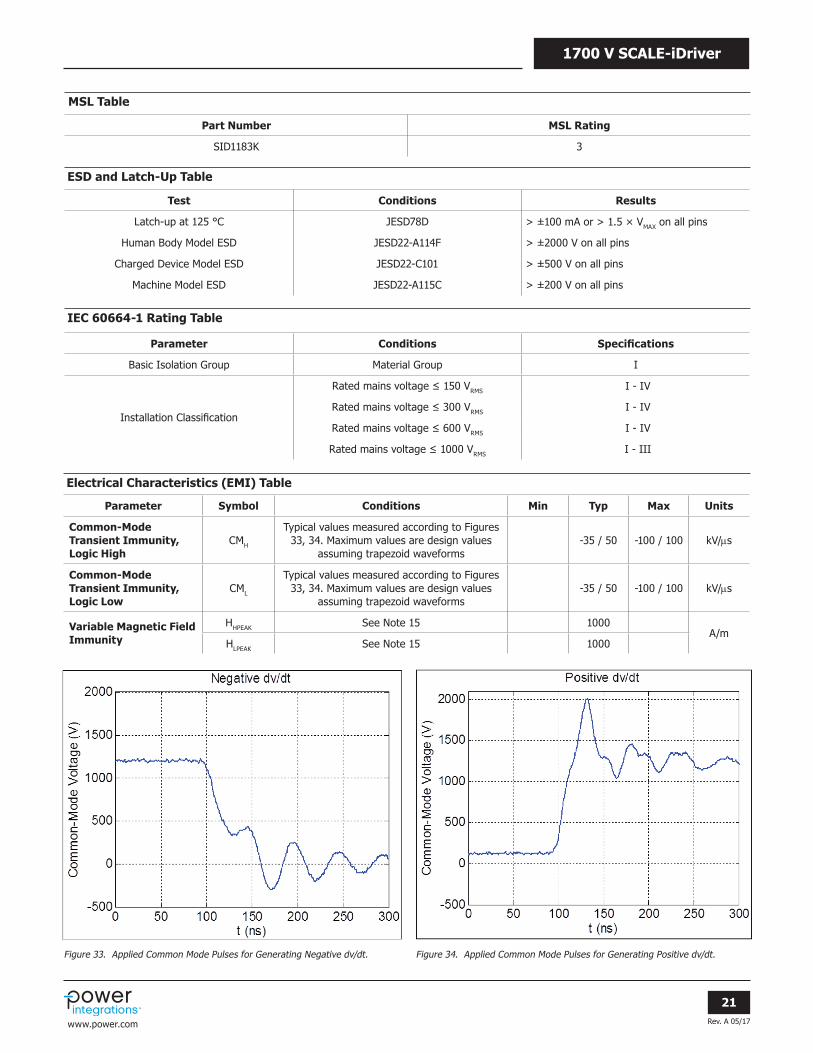
Common-Mode Transient Immunity, Logic High
CMH
Typical values measured according to Figures 33, 34. Maximum values are design values
assuming trapezoid waveforms-35 / 50 -100 / 100 kV/µs
Common-Mode Transient Immunity, Logic Low
CML
Typical values measured according to Figures 33, 34. Maximum values are design values
assuming trapezoid waveforms-35 / 50 -100 / 100 kV/µs
Variable Magnetic Field Immunity
HHPEAK See Note 15 1000A/m
HLPEAK See Note 15 1000
Figure 33. Applied Common Mode Pulses for Generating Negative dv/dt. Figure 34. Applied Common Mode Pulses for Generating Positive dv/dt.
Rev. A 05/17
22
1700 V SCALE-iDriver
www.power.com
Regulatory Information Table
VDE UL CSA
Certified to DIN V VDE V 0884-10 (VDE V 0884-10): 2006-12
UR recognized under UL1577 Component Recognition Program
UR recognized to CSA Component Acceptance Notice 5A
Basic insulation for Max. Transient Isolation voltage 8 kVPEAK, Max. Surge Isolation voltage 8 kVPEAK, Max. Repetitive Peak Isolation voltage 1700 VPEAK
Single protection, 5000 VRMS dielectric voltage withstand
Single protection, 5000 VRMS dielectric voltage withstand
File No. 5020828-4880-0002 File No. Pending File No. Pending
Part Ordering Information
• SCALE-iDriver Product Family
• Series Number
• Package Identifier
K eSOP-R16B
• Tape & Reel and Other Options
Blank Tube of 48 pcs.
TL Tape & Reel, 1000 pcs min/mult.SID 1183 K - TL
Revision Notes Date
A Code A Initial Release. 05/17
For the latest updates, visit our website: www.power.comPower Integrations reserves the right to make changes to its products at any time to improve reliability or manufacturability. Power Integrations does not assume any liability arising from the use of any device or circuit described herein. POWER INTEGRATIONS MAKES NO WARRANTY HEREIN AND SPECIFICALLY DISCLAIMS ALL WARRANTIES INCLUDING, WITHOUT LIMITATION, THE IMPLIED WARRANTIES OF MERCHANTABILITY, FITNESS FOR A PARTICULAR PURPOSE, AND NON-INFRINGEMENT OF THIRD PARTY RIGHTS.
Patent InformationThe products and applications illustrated herein (including transformer construction and circuits external to the products) may be covered by one or more U.S. and foreign patents, or potentially by pending U.S. and foreign patent applications assigned to Power Integrations. A complete list of Power Integrations patents may be found at www.power.com. Power Integrations grants its customers a license under certain patent rights as set forth at http://www.power.com/ip.htm.
Life Support PolicyPOWER INTEGRATIONS PRODUCTS ARE NOT AUTHORIZED FOR USE AS CRITICAL COMPONENTS IN LIFE SUPPORT DEVICES OR SYSTEMS WITHOUT THE EXPRESS WRITTEN APPROVAL OF THE PRESIDENT OF POWER INTEGRATIONS. As used herein:
1. A Life support device or system is one which, (i) is intended for surgical implant into the body, or (ii) supports or sustains life, and (iii) whose failure to perform, when properly used in accordance with instructions for use, can be reasonably expected to result in significant injury or death to the user.
2. A critical component is any component of a life support device or system whose failure to perform can be reasonably expected to cause the failure of the life support device or system, or to affect its safety or effectiveness.
The PI logo, TOPSwitch, TinySwitch, SENZero, SCALE, SCALE-iDriver, Qspeed, PeakSwitch, LYTSwitch, LinkZero, LinkSwitch, InnoSwitch, HiperTFS, HiperPFS, HiperLCS, DPA-Switch, CAPZero, Clampless, EcoSmart, E-Shield, Filterfuse, FluxLink, StakFET, PI Expert and PI FACTS are trademarks of Power Integrations, Inc. Other trademarks are property of their respective companies. ©2017, Power Integrations, Inc.
World Headquarters5245 Hellyer AvenueSan Jose, CA 95138, USAMain: +1-408-414-9200Customer Service:Worldwide: +1-65-635-64480Americas: +1-408-414-9621e-mail: [email protected]
China (Shanghai)Rm 2410, Charity Plaza, No. 88North Caoxi RoadShanghai, PRC 200030Phone: +86-21-6354-6323e-mail: [email protected]
China (Shenzhen)17/F, Hivac Building, No. 2, Keji Nan 8th Road, Nanshan District, Shenzhen, China, 518057Phone: +86-755-8672-8689e-mail: [email protected]
Germany (AC-DC/LED Sales)Lindwurmstrasse 114D-80337 MünchenGermanyPhone: +49-89-5527-39100e-mail: [email protected]
Germany (IGBT Driver Sales)HellwegForum 159469 EnseGermany Tel: +49-2938-64-39990e-mail: igbt-driver.sales@ power.com
India#1, 14th Main RoadVasanthanagarBangalore-560052 IndiaPhone: +91-80-4113-8020e-mail: [email protected]
ItalyVia Milanese 20, 3rd. Fl.20099 Sesto San Giovanni (MI) ItalyPhone: +39-024-550-8701e-mail: [email protected]
JapanKosei Dai-3 Bldg. 2-12-11, Shin-Yokohama, Kohoku-ku Yokohama-shi, Kanagawa 222-0033 JapanPhone: +81-45-471-1021e-mail: [email protected]
KoreaRM 602, 6FLKorea City Air Terminal B/D, 159-6Samsung-Dong, Kangnam-Gu,Seoul, 135-728, KoreaPhone: +82-2-2016-6610e-mail: [email protected]
Singapore51 Newton Road#19-01/05 Goldhill PlazaSingapore, 308900Phone: +65-6358-2160e-mail: [email protected]
Taiwan5F, No. 318, Nei Hu Rd., Sec. 1Nei Hu Dist.Taipei 11493, Taiwan R.O.C.Phone: +886-2-2659-4570e-mail: [email protected]
UKBuilding 5, Suite 21The Westbrook CentreMilton RoadCambridge CB4 1YGPhone: +44 (0) 7823-557484e-mail: [email protected]
Power Integrations Worldwide Sales Support Locations