16 rf frequency (ghz)lo rl lo return loss -7 -6 db rf rl rf return loss @ gain max rf return loss @...
TRANSCRIPT
CHR3662-QDG RoHS COMPLIANT
Ref. : DSCHR3662-QDG1192 - 11 Jul 11 1/16 Specifications subject to change without notice
United Monolithic Semiconductors S.A.S. Route Départementale 128 - BP46 - 91401 Orsay Cedex France
Tel.: +33 (0) 1 69 33 03 08 - Fax: +33 (0) 1 69 33 03 09
7-16GHz Integrated Down Converter
GaAs Monolithic Microwave IC in SMD package
Description The CHR3662-QDG is a multifunction part, which integrates a balanced cold FET mixer, a LO buffer, and a RF LNA including gain control. It is designed for a wide range of applications, typically commercial communication systems. The circuit is manufactured with a pHEMT process 0.25µm. It is available in lead-free SMD package.
Main Features
■ Broadband RF performance 7-16GHz
■ 13dB gain
■ 15dBc Image Frequency Rejection
■ 0dBm Input IP3
■ 15dB Gain control
■ 24LQFN4x4
■ ESD protected
■ MSL Level: 1
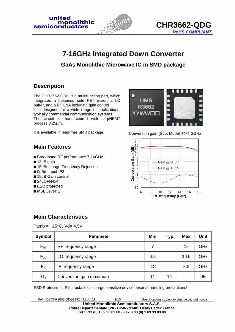
Conversion gain (Sup. Mode) @FI=2GHz
Main Characteristics
Tamb = +25°C, Vd= 4.5V
Symbol Parameter Min Typ Max Unit
FRF RF frequency range 7 16 GHz
FLO LO frequency range 4.5 19.5 GHz
FIF IF frequency range DC 3.5 GHz
Gc Conversion gain maximum 11 14 dB
ESD Protections: Electrostatic discharge sensitive device observe handling precautions!
-10-8-6-4-202468
101214161820
6 8 10 12 14 16 18
RF frequency (GHz)
Co
nv
ers
ion
Ga
in (
dB
)
Gain @ -1.5V
Gain @ +0.5V
UMS
A3667A
YYWWG
UMS
A3667A
YYWWG
UMS
A3688A
YYWWG
UMS
A3667A
YYWWG
UMS
A3667A
YYWWG
UMS
A3688A
YYWWG
UMS R3662
YYWW
CHR3662-QDG 7-16GHz Down Converter
Ref. : DSCHR3662-QDG1192 - 11 Jul 11 2/16 Specifications subject to change without notice
Route Départementale 128, BP46 - 91401 ORSAY Cedex - FRANCE
Tel.: +33 (0) 1 69 33 03 08 - Fax: +33 (0) 1 69 33 03 09
Electrical Characteristics
Tamb = +25°C, Vd= 4.5V
Symbol Parameter Min Typ Max Unit
FRF RF frequency range 7 16 GHz
FLO LO frequency range 4.5 19.5 GHz
FIF IF frequency range DC 3.5 GHz
Gc Conversion gain @ V2_V3=-1.5V (1) (gain max)
Conversion gain @ V2_V3=+0.5V (1) (gain min)
11 14
-4
-2
dB
dB
G Gain control range 13 15 dB
NF Noise Figure @ V2_V3=-1.5V (gain max), for IF>0.1GHz
3 3.5 dB
IFR Image Frequency Rejection (1) 13 15 dBc
PLO LO Input power 0 dBm
IIP3 Input IP3@ gain max.
Input IP3 all attenuation
0
-3
dBm
LO RL LO Return Loss -7 -6 dB
RF RL RF Return Loss @ Gain max
RF Return Loss @ Gain min
-9
-5
-6
-4 dB
LO/RF LO leakage at RF port @ max. gain -35 dBm
Vd DC drain voltage 4.5 V
Id Drain current 210 280 350 mA
VG DC gate voltage LNA -0.3 V
V2_V3 DC gain control voltage -1.5 0.5 V
B DC gate control voltage LO buffer -5 V
VGM DC gate voltage mixer -1 V
(1) An external combiner 90° is necessary on I / Q. Note: Id is not affected by V2, V3. These values are representative of onboard measurements as defined on the drawing given in the paragraph “Evaluation mother board".
7-16GHz Down Converter CHR3662-QDG
Ref.: DSCHR3662-QDG1192 - 11 Jul 11 3/16 Specifications subject to change without notice
Route Départementale 128, BP46 - 91401 ORSAY Cedex - FRANCE
Tel.: +33 (0) 1 69 33 03 08 - Fax: +33 (0) 1 69 33 03 09
Absolute Maximum Ratings (1)
Tamb = +25°C
Symbol Parameter Values Unit
Vd Maximum drain bias voltage 5 V
Id Maximum drain bias current 400 mA
VG, VGM Gate bias voltage range -2.0 to +0.6 V
V2,V3 Gain control voltage range -2.0 to +1 V
P_RF Maximum peak input power overdrive 10 dBm
PLO Maximum LO input power 10 dBm
Tch Maximum channel temperature 175 °C
Ta Operating temperature range -40 to +85 °C
Tstg Storage temperature range -55 to +125 °C
(1) Operation of this device above anyone of these parameters may cause permanent damage.
CHR3662-QDG 7-16GHz Down Converter
Ref. : DSCHR3662-QDG1192 - 11 Jul 11 4/16 Specifications subject to change without notice
Route Départementale 128, BP46 - 91401 ORSAY Cedex - FRANCE
Tel.: +33 (0) 1 69 33 03 08 - Fax: +33 (0) 1 69 33 03 09
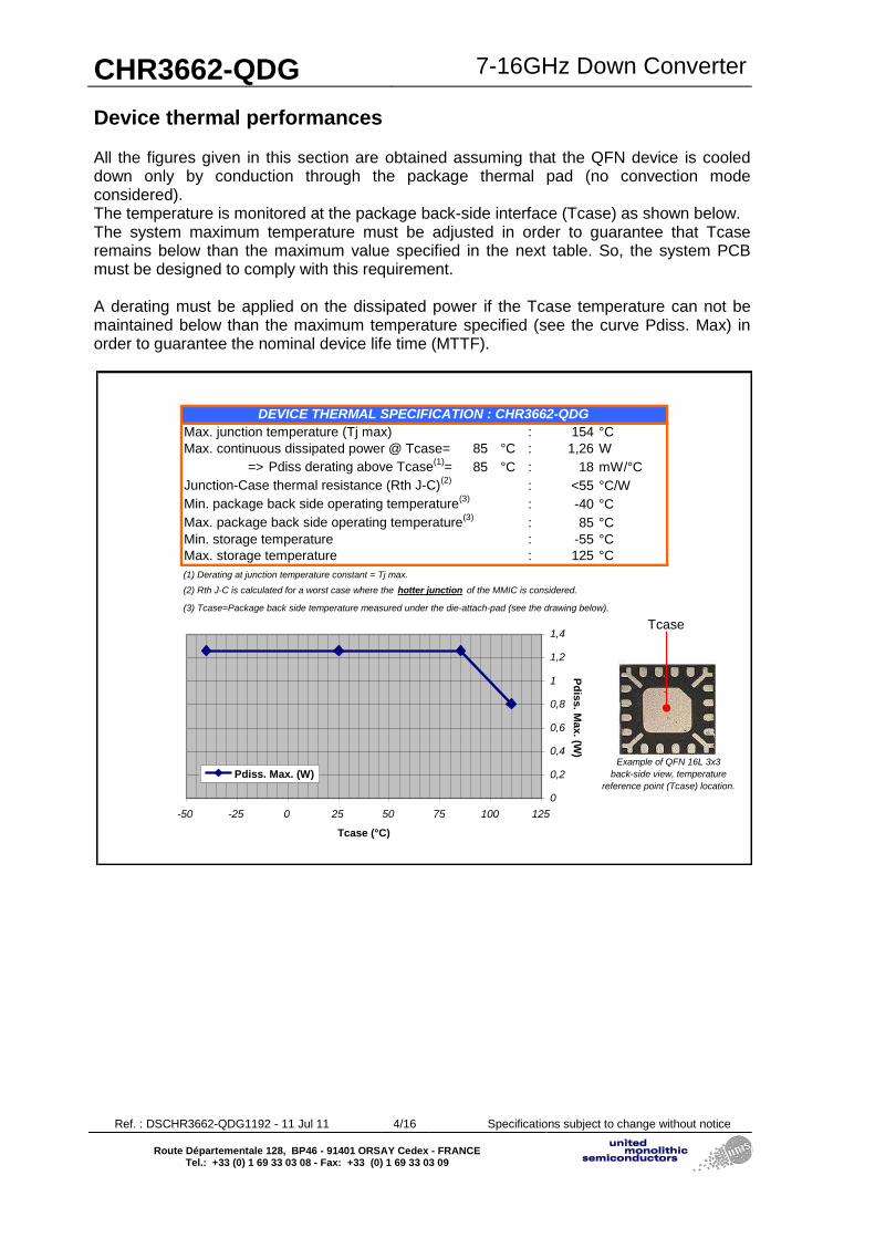
Device thermal performances All the figures given in this section are obtained assuming that the QFN device is cooled down only by conduction through the package thermal pad (no convection mode considered). The temperature is monitored at the package back-side interface (Tcase) as shown below. The system maximum temperature must be adjusted in order to guarantee that Tcase remains below than the maximum value specified in the next table. So, the system PCB must be designed to comply with this requirement. A derating must be applied on the dissipated power if the Tcase temperature can not be maintained below than the maximum temperature specified (see the curve Pdiss. Max) in order to guarantee the nominal device life time (MTTF).
Max. junction temperature (Tj max) : 154 °C
Max. continuous dissipated power @ Tcase= 85 °C : 1,26 W
=> Pdiss derating above Tcase(1)
= 85 °C : 18 mW/°C
Junction-Case thermal resistance (Rth J-C)(2)
: <55 °C/W
Min. package back side operating temperature(3)
: -40 °C
Max. package back side operating temperature(3)
: 85 °C
Min. storage temperature : -55 °C
Max. storage temperature : 125 °C
(1) Derating at junction temperature constant = Tj max.
(2) Rth J-C is calculated for a worst case where the hotter junction of the MMIC is considered.
(3) Tcase=Package back side temperature measured under the die-attach-pad (see the drawing below).
DEVICE THERMAL SPECIFICATION : CHR3662-QDG
0
0,2
0,4
0,6
0,8
1
1,2
1,4
-50 -25 0 25 50 75 100 125
Tcase (°C)
Pd
iss. M
ax. (W
)
Pdiss. Max. (W)
Tcase
Example of QFN 16L 3x3
back-side view, temperature
reference point (Tcase) location.

7-16GHz Down Converter CHR3662-QDG
Ref.: DSCHR3662-QDG1192 - 11 Jul 11 5/16 Specifications subject to change without notice
Route Départementale 128, BP46 - 91401 ORSAY Cedex - FRANCE
Tel.: +33 (0) 1 69 33 03 08 - Fax: +33 (0) 1 69 33 03 09
Typical Measured Performances
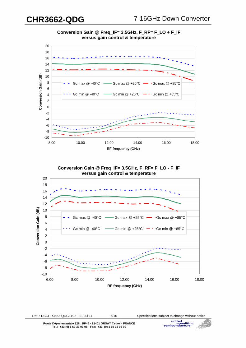
Tamb = +25°C, VD = 4.5V, Typical B = -5V & VG = -0.3V & VGM = -1V, P_LO=0dBm These values are representative of onboard measurements (on connectors access planes) as defined on the drawing 97342 page 14. The board loss is estimated to 0.5 to 1.5dB in the frequency range.
Conversion Gain @ Freq_IF= 2GHz, F_RF= F_LO + F_IF versus gain control & temperature
Conversion Gain @ Freq_IF= 2GHz, F_RF= F_LO - F_IF versus gain control & temperature
-10
-8
-6
-4
-2
0
2
4
6
8
10
12
14
16
18
20
6,00 8,00 10,00 12,00 14,00 16,00 18,00
RF frequency (GHz)
Co
nvers
ion
Gain
(d
B)
Gc max @ -40°C Gc max @ +25°C Gc max @ +85°C
Gc min @ -40°C Gc min @ +25°C Gc min @ +85°C
-10
-8
-6
-4
-2
0
2
4
6
8
10
12
14
16
18
20
6,00 8,00 10,00 12,00 14,00 16,00 18,00
RF frequency (GHz)
Co
nvers
ion
Gain
(d
B)
Gc max @ -40°C Gc max @ +25°C Gc max @ +85°C
Gc min @ -40°C Gc min @ +25°C Gc min @ +85°C
CHR3662-QDG 7-16GHz Down Converter
Ref. : DSCHR3662-QDG1192 - 11 Jul 11 6/16 Specifications subject to change without notice
Route Départementale 128, BP46 - 91401 ORSAY Cedex - FRANCE
Tel.: +33 (0) 1 69 33 03 08 - Fax: +33 (0) 1 69 33 03 09
Conversion Gain @ Freq_IF= 3.5GHz, F_RF= F_LO + F_IF versus gain control & temperature
Conversion Gain @ Freq_IF= 3.5GHz, F_RF= F_LO - F_IF versus gain control & temperature
-10
-8
-6
-4
-2
0
2
4
6
8
10
12
14
16
18
20
8,00 10,00 12,00 14,00 16,00 18,00
RF frequency (GHz)
Co
nv
ers
ion
Ga
in (
dB
)
Gc max @ -40°C Gc max @ +25°C Gc max @ +85°C
Gc min @ -40°C Gc min @ +25°C Gc min @ +85°C
-10
-8
-6
-4
-2
0
2
4
6
8
10
12
14
16
18
20
6.00 8.00 10.00 12.00 14.00 16.00 18.00
RF frequency (GHz)
Co
nv
ers
ion
Ga
in (
dB
)
Gc max @ -40°C Gc max @ +25°C Gc max @ +85°C
Gc min @ -40°C Gc min @ +25°C Gc min @ +85°C

7-16GHz Down Converter CHR3662-QDG
Ref.: DSCHR3662-QDG1192 - 11 Jul 11 7/16 Specifications subject to change without notice
Route Départementale 128, BP46 - 91401 ORSAY Cedex - FRANCE
Tel.: +33 (0) 1 69 33 03 08 - Fax: +33 (0) 1 69 33 03 09
V2=V3=+0.5V
V2=V3=-1.5V
Image rejection @ Freq_IF= 2GHz, V2=V3=-1.5V versus temperature
Noise figure @ Freq_IF= 2GHz versus gain & temperature
Rem: The losses due to board are removed for noise measurements.
0
2
4
6
8
10
12
14
16
18
20
22
24
26
28
6 8 10 12 14 16 18
LO frequency (GHz)
Ima
ge
re
jec
tio
n (
dB
)
-40°C +25°C +85°C
0
1
2
3
4
5
6
7
8
9
10
11
12
13
14
15
16
6,00 8,00 10,00 12,00 14,00 16,00 18,00
RF frequency (GHz)
No
ise f
igu
re (
dB
)
-40°C +25°C +85°C
-40°C +25°C +85°C

CHR3662-QDG 7-16GHz Down Converter
Ref. : DSCHR3662-QDG1192 - 11 Jul 11 8/16 Specifications subject to change without notice
Route Départementale 128, BP46 - 91401 ORSAY Cedex - FRANCE
Tel.: +33 (0) 1 69 33 03 08 - Fax: +33 (0) 1 69 33 03 09
Noise figure @ Freq_IF= 2GHz versus V2,V3 at 25°C
Rem: The losses due to board are removed for noise measurements.
Associated gain @ Freq_IF= 2GHz versus V2,V3 at 25°C
0
1
2
3
4
5
6
7
8
9
10
11
12
13
14
15
16
6,00 8,00 10,00 12,00 14,00 16,00 18,00
RF frequency (GHz)
No
ise
fig
ure
(d
B)
-1.5V -0.5V -0.2V -0.1V +0.5V
-10
-8
-6
-4
-2
0
2
4
6
8
10
12
14
16
6 8 10 12 14 16 18
RF frequency (GHz)
As
so
cia
ted
ga
in (
dB
)
-1.5V -0.5V -0.2V -0.1V +0.5V
7-16GHz Down Converter CHR3662-QDG
Ref.: DSCHR3662-QDG1192 - 11 Jul 11 9/16 Specifications subject to change without notice
Route Départementale 128, BP46 - 91401 ORSAY Cedex - FRANCE
Tel.: +33 (0) 1 69 33 03 08 - Fax: +33 (0) 1 69 33 03 09
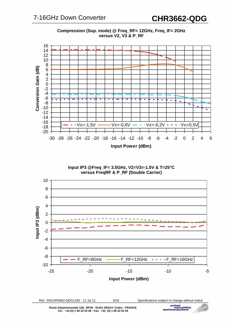
Compression (Sup. mode) @ Freq_RF= 12GHz, Freq_IF= 2GHz versus V2, V3 & P_RF
Input IP3 @Freq_IF= 3.5GHz, V2=V3=-1.5V & T=25°C versus FreqRF & P_RF (Double Carrier)
-20-18-16-14-12-10-8-6-4-202468
10121416
-30 -28 -26 -24 -22 -20 -18 -16 -14 -12 -10 -8 -6 -4 -2 0 2 4 6
Input Power (dBm)
Co
nvers
ion
Gain
(d
B)
Vx=-1,5V Vx=-0,6V Vx=-0,2V Vx=0,5V
-10
-8
-6
-4
-2
0
2
4
6
8
10
-25 -20 -15 -10 -5
Input Power (dBm)
Inp
ut
IP3 (
dB
m)
F_RF=8GHz F_RF=12GHz F_RF=16GHz

CHR3662-QDG 7-16GHz Down Converter
Ref. : DSCHR3662-QDG1192 - 11 Jul 11 10/16 Specifications subject to change without notice
Route Départementale 128, BP46 - 91401 ORSAY Cedex - FRANCE
Tel.: +33 (0) 1 69 33 03 08 - Fax: +33 (0) 1 69 33 03 09
Input IP3 @Freq_RF=12GHz, Freq_IF= 3.5GHz & V2=V3=-1.5V versus T & P_RF (Double Carrier)
Input IP3 @Freq_RF=12GHz, Freq_IF= 3.5GHz & T=25°C versus V2,V3 & P_RF (Double Carrier)
-10
-8
-6
-4
-2
0
2
4
6
8
10
-25 -20 -15 -10 -5
Input Power (dBm)
Inp
ut
IP3 (
dB
m)
T=-40°C T=25°C T=85°C
-10
-8
-6
-4
-2
0
2
4
6
8
10
12
14
16
18
20
-20 -15 -10
Input Power (dBm)
Inp
ut
IP3 (
dB
m)
Vx=-1,5V Vx=-0,6V Vx=-0,2V
7-16GHz Down Converter CHR3662-QDG
Ref.: DSCHR3662-QDG1192 - 11 Jul 11 11/16 Specifications subject to change without notice
Route Départementale 128, BP46 - 91401 ORSAY Cedex - FRANCE
Tel.: +33 (0) 1 69 33 03 08 - Fax: +33 (0) 1 69 33 03 09
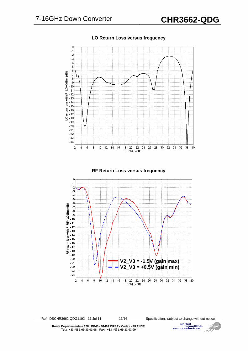
LO Return Loss versus frequency
RF Return Loss versus frequency
V2_V3 = -1.5V (gain max)
V2_V3 = +0.5V (gain min)

CHR3662-QDG 7-16GHz Down Converter
Ref. : DSCHR3662-QDG1192 - 11 Jul 11 12/16 Specifications subject to change without notice
Route Départementale 128, BP46 - 91401 ORSAY Cedex - FRANCE
Tel.: +33 (0) 1 69 33 03 08 - Fax: +33 (0) 1 69 33 03 09
Package outline (1)
Matt tin, Lead Free
(Green) 1- Nc 13- Gnd
Units mm 2- Gnd 14- Gnd
From the standard JEDEC MO-220 3- Gnd 15- LO
(VGGD) 4- RF 16- Gnd
25- GND 5- Gnd 17- Gnd
6- Gnd 18- Nc
7- V2 19- I
8- V3 20- Gnd
9- VG 21- Gnd
10- VGM 22- Q
11- VD 23- Nc
12- B 24- Nc
(1)The package outline drawing included to this data-sheet is given for indication. Refer to the
application note AN0017 available at http://www.ums-gaas.com for exact package dimensions. It is strongly recommended to ground all pins marked “Gnd” through the PCB board. Ensure that the PCB board is designed to provide the best possible ground to the package.
R3662
7-16GHz Down Converter CHR3662-QDG
Ref.: DSCHR3662-QDG1192 - 11 Jul 11 13/16 Specifications subject to change without notice
Route Départementale 128, BP46 - 91401 ORSAY Cedex - FRANCE
Tel.: +33 (0) 1 69 33 03 08 - Fax: +33 (0) 1 69 33 03 09
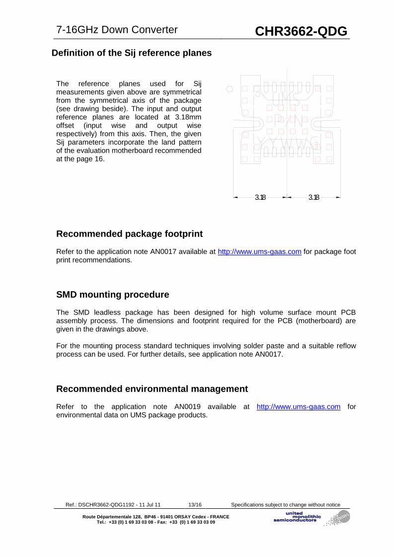
Definition of the Sij reference planes The reference planes used for Sij measurements given above are symmetrical from the symmetrical axis of the package (see drawing beside). The input and output reference planes are located at 3.18mm offset (input wise and output wise respectively) from this axis. Then, the given Sij parameters incorporate the land pattern of the evaluation motherboard recommended at the page 16.
Recommended package footprint Refer to the application note AN0017 available at http://www.ums-gaas.com for package foot print recommendations.
SMD mounting procedure The SMD leadless package has been designed for high volume surface mount PCB assembly process. The dimensions and footprint required for the PCB (motherboard) are given in the drawings above. For the mounting process standard techniques involving solder paste and a suitable reflow process can be used. For further details, see application note AN0017.
Recommended environmental management Refer to the application note AN0019 available at http://www.ums-gaas.com for environmental data on UMS package products.
3.18 3.18
CHR3662-QDG 7-16GHz Down Converter
Ref. : DSCHR3662-QDG1192 - 11 Jul 11 14/16 Specifications subject to change without notice
Route Départementale 128, BP46 - 91401 ORSAY Cedex - FRANCE
Tel.: +33 (0) 1 69 33 03 08 - Fax: +33 (0) 1 69 33 03 09
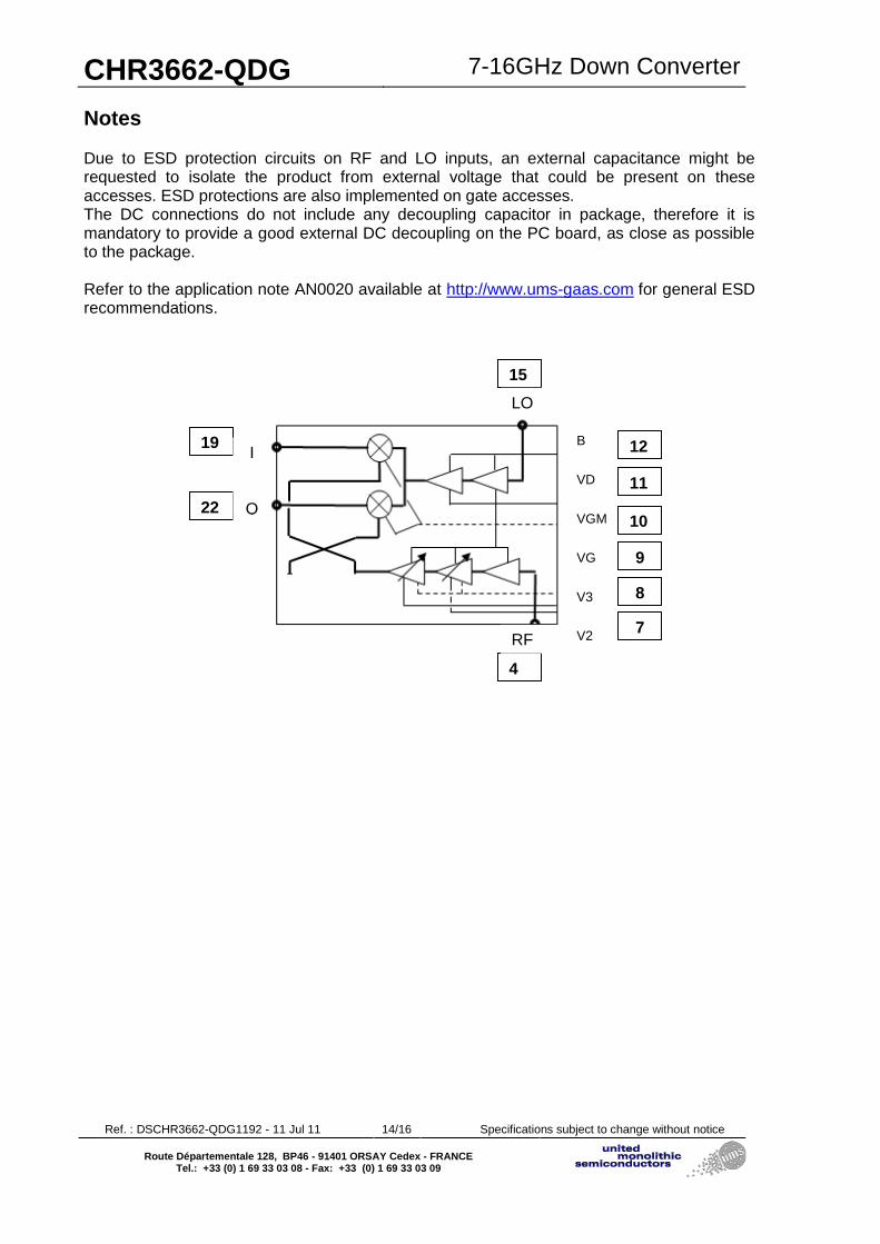
B
VD
VGM
VG
V3
V2
Notes Due to ESD protection circuits on RF and LO inputs, an external capacitance might be requested to isolate the product from external voltage that could be present on these accesses. ESD protections are also implemented on gate accesses. The DC connections do not include any decoupling capacitor in package, therefore it is mandatory to provide a good external DC decoupling on the PC board, as close as possible to the package. Refer to the application note AN0020 available at http://www.ums-gaas.com for general ESD recommendations.
9
11
4
7
22
8
15
12 19
10
I
Q
RF
LO

7-16GHz Down Converter CHR3662-QDG
Ref. : DSCHR3662-QDG1192 - 11 Jul 11 15/16 Specifications subject to change without notice
Route Départementale 128, BP46 - 91401 ORSAY Cedex - FRANCE Tel.: +33 (0) 1 69 33 03 08 - Fax: +33 (0) 1 69 33 03 09
Notes The biasing circuits of the stages of the circuit are given in the schemes below.
V3
70300
1.5k 40
Vd=4.5V
35
100 100
18
Vg=-0.3V
Stage 1 Stage 2
Stage 3
2.8k
2.8k
V2LNA
IN
OUT
V3
70300
1.5k 40
Vd=4.5V
35
100 100
18
Vg=-0.3V
Stage 1 Stage 2
Stage 3
2.8k
2.8k
V2LNA
IN
OUT
1.8k
2k
B=-5V
Stage 1
780
1.5k
Stage 2
1.5k
300
300
25 8
Vd=4.5V
LO
LO IN
LO OUT
1.8k
2k
B=-5V
Stage 1
780
1.5k
Stage 2
1.5k
300
300
25 8
Vd=4.5V
LO
LO IN
LO OUT
CHR3662-QDG 7-16GHz Down Converter
Ref. : DSCHR3662-QDG1192 - 11 Jul 11 16/16 Specifications subject to change without notice
Route Départementale 128, BP46 - 91401 ORSAY Cedex - FRANCE
Tel.: +33 (0) 1 69 33 03 08 - Fax: +33 (0) 1 69 33 03 09
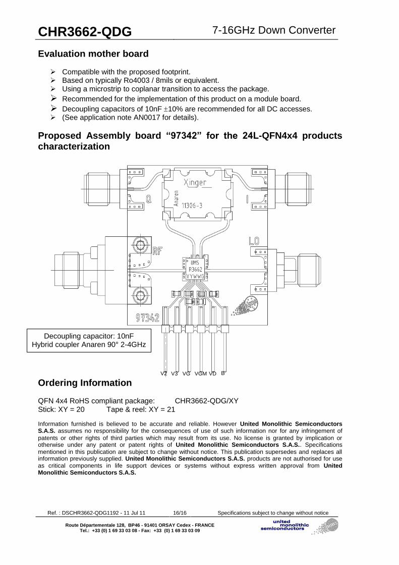
Evaluation mother board Compatible with the proposed footprint. Based on typically Ro4003 / 8mils or equivalent. Using a microstrip to coplanar transition to access the package.
Recommended for the implementation of this product on a module board. Decoupling capacitors of 10nF 10% are recommended for all DC accesses. (See application note AN0017 for details).
Proposed Assembly board “97342” for the 24L-QFN4x4 products characterization
Ordering Information QFN 4x4 RoHS compliant package: CHR3662-QDG/XY Stick: XY = 20 Tape & reel: XY = 21 Information furnished is believed to be accurate and reliable. However United Monolithic Semiconductors S.A.S. assumes no responsibility for the consequences of use of such information nor for any infringement of
patents or other rights of third parties which may result from its use. No license is granted by implication or otherwise under any patent or patent rights of United Monolithic Semiconductors S.A.S.. Specifications
mentioned in this publication are subject to change without notice. This publication supersedes and replaces all information previously supplied. United Monolithic Semiconductors S.A.S. products are not authorised for use as critical components in life support devices or systems without express written approval from United Monolithic Semiconductors S.A.S.
V2 V3 VG VGM VD B
Decoupling capacitor: 10nF Hybrid coupler Anaren 90° 2-4GHz