159233 computer architecture building up the …plyons/159233 (computer... · · 2010-02-18t r a...
TRANSCRIPT

© Paul Lyons 2010~ 1 ~
159233 Computer Architecture
159233
Computer Architecture
© Paul Lyons 2010~ 2 ~
159233 Computer Architecture
INTRODUCTION 2IC FABRICATION 7THE ISA 14REPRESENTING HLL CONSTRUCTS 30PERFORMANCE 35COMPUTER ARITHMETIC 49BUILDING UP THE DATAPATH 54FLOATING POINT NUMBERS 70SINGLE-CYCLE ARCHITECTURE 78MULTI-CYCLE ARCHITECTURE 109PIPELINING 125EXCEPTIONS 155MEMORY MANAGEMENT 157
cache 165virtual memory 199
© Paul Lyons 2010~ 3 ~
159233 Computer Architecture
INTRODUCTION
Physical properties
ABSTRACTION
Concepts
A device
sector
track
Concepts
© Paul Lyons 2010~ 4 ~
159233 Computer Architecture
LEVELS OF ABSTRACTION
INTRODUCTION
Computer systems use technology to simulate the human world
Human thought processes
ISA
GatesData processing modules
native data typesinstruction setregistersaddressing modes
interruptsexception handling
I/O handling
Transistors
cycles per instruction physical registers
Machine code
Assembly language
High level languages
01100000101011
add A, B
C = (A + B)*3

© Paul Lyons 2010~ 5 ~
159233 Computer Architecture
AGENERIC COMPUTER
INTRODUCTION
processor
© Paul Lyons 2010~ 6 ~
159233 Computer Architecture
MEMORY HIERARCHY
INTRODUCTION
© Paul Lyons 2010~ 7 ~
159233 Computer Architecture
THE IC INDUSTRY
IC FABRICATION
Very large market
Very few products
High rate of development
Long development times
Multiple generations in simultaneous development
Discontinuous technological change
© Paul Lyons 2010~ 8 ~
159233 Computer Architecture
PRODUCING THE WAFERS
IC FABRICATION

© Paul Lyons 2010~ 9 ~
159233 Computer Architecture
IC FABRICATION
Si Si
Si
Si Si
Si
Si
SiSi Si
Si
SiSiSi
Si
Si
DOPING THE WAFER
P
-
-
-
-
-
+
+
+
+
+
© Paul Lyons 2010~ 10 ~
159233 Computer Architecture
HOW ACMOSTRANSISTOR WORKS
IC FABRICATION
+ + ++ + ++ + ++ + ++ + +
+-
© Paul Lyons 2010~ 11 ~
159233 Computer Architecture
MAKING ACMOSTRANSISTOR
IC FABRICATION
© Paul Lyons 2010~ 12 ~
159233 Computer Architecture
MAKING ACMOSTransistor
IC FABRICATION

© Paul Lyons 2010~ 13 ~
159233 Computer Architecture
MAKING ACMOSTRANSISTOR
IC FABRICATION
+ + + + + +
+-
© Paul Lyons 2010~ 14 ~
159233 Computer Architecture
THE MIPSCOMPUTER
THE ISA
a popular microprocessor(a billion sold?)
RISC architecture
CISC RISC
slow memory, assembly language era fast memory, HLL era
simple instructions cut clock cycles to 1compilers issue complex instruction sequences
single addressing mode per instructioninstructions that operate only on registers
small controller large no. of registershardwired instructions
© Paul Lyons 2010~ 16 ~
159233 Computer Architecture
THE MIPSCOMPUTER
THE ISA
a popular microprocessor(a billion sold?)
RISC architecture
Architecture
Machine Language
Instruction Set
Compilers
Design Goal
© Paul Lyons 2010~ 17 ~
159233 Computer Architecture
THE ADD INSTRUCTION
THE ISA
The MIPS computer has a 3-address architecture
add a, b, csub a, b, c
# a = b + c# a = b - c
add a, b, cadd a, a, dadd a, a, e
# a = b + c# a = a + d# a = a + e# a contains the sum of b, c, d, & e
move $8, $19 # r8 � #r19 - desired behaviour
add $8, $0, $19 # r8 � 0 + $19 - actual implementation

© Paul Lyons 2010~ 18 ~
159233 Computer Architecture
EXPRESSION TREES AND EVALUATION ORDER
THE ISA
+
+
b c
+
d e
+
bc
+
d
+
e
a
a
a
a f
a
© Paul Lyons 2010~ 19 ~
159233 Computer Architecture
THE REGISTERS
THE ISA
$0, $1, … $31
address calculation, stack pointers as well as data storage
© Paul Lyons 2010~ 20 ~
159233 Computer Architecture
THE REGISTERS
THE ISA
Register Name(s) Use
0 $zero12-3 $v0-$v14-7 $a0-$a38-15 $t0-$t716-23 $s0-$s724-25 $t8-$t926-27 28 $gp29 $sp30 $fp31 $ra
© Paul Lyons 2010~ 21 ~
159233 Computer Architecture
RISCDESIGNS FAVOUR SIMPLICITY
THE ISA
32-bit instructionstwo types: R(egister) –type & I(mmediate)-type
op rs rt rd shamt functR-type
6 bits 5 bits 5 bits 5 bits 5 bits 6 bits

© Paul Lyons 2010~ 22 ~
159233 Computer Architecture
RISCDESIGNS FAVOUR SIMPLICITY
THE ISA
I-type op rs rt constant or address
op rs rt rd shamt functR-type
6 bits 5 bits 5 bits 5 bits 5 bits 6 bits
have a constant operandor access memory
32-bit instructionstwo types: R(egister) –type & I(mmediate)-type
© Paul Lyons 2010~ 23 ~
159233 Computer Architecture
RISCDESIGNS FAVOUR SIMPLICITY
THE ISA
(Yeah, right)
I-type op rs rt constant or address
load $t0 with the word in $s2 plus the word 8 up from the address in $s3lw $t0, 32($s3)
add $t0, $s2, $t0
let’s say x is in register called $t0 in the assembler, actual reg. 8h is in register called $s2 in the assembler, actual reg.18array a starts at the location contained in reg.$s3, actual reg.19
x = h + a[8]
35 19 8 32
(psst; there's a third type as well; J-type, for jump instructions)regularity is an ideal, but good compromises must sometimes be made
© Paul Lyons 2010~ 24 ~
159233 Computer Architecture
COMPILATION
THE ISA
HLL code
expression treevariable-registerassociations
assembler
f = (g+h) – (i+j)
$s1 $s2 $s3 $s4
name registerf $s0g $s1h $s2I $s3j $s4
+$t0 + $t1
-$s0
machine code
memory image
© Paul Lyons 2010~ 25 ~
159233 Computer Architecture
REGISTER��MEMORYTRANSFERS
THE ISA
complex programs are difficult to write, with only 32 registers
instructions for storing data to memory and loading data from memory
memory works like a big 1-D array, addressed by byte
if $19 contains start, then lw $8, 12($19)
loads 1 into register $8
100 1000 10 1start start
+ 4start+ 8
start+ 12

© Paul Lyons 2010~ 26 ~
159233 Computer Architecture
MORE ABOUT MEMORY
THE ISA
Compiler also allocates
232 bytes230 words
4,294,967,2961,073,741,824
Large address space means access times
Compiler tries to keeps spills
© Paul Lyons 2010~ 27 ~
159233 Computer Architecture
BRANCHES
THE ISA
Computers must have
mostly, that's just that's why
sometimes it needs to that's why the PC is the choice depends on
beq $1, $2, L1 # branch to L1 if $1 and $2 are equal
PC is loaded with PC is incremented
bne $1, $2, L1 # branch to L1 if $1 and $2 not equal
© Paul Lyons 2010~ 28 ~
159233 Computer Architecture
TESTS USING INEQUALITY
THE ISA
SLT (Set on Less Than)compares SLT $r1, $r2, $r3
C Equivalent:
BLT (Branch on Less Than)
would need simpler & more regular to use
© Paul Lyons 2010~ 29 ~
159233 Computer Architecture
SLTI (Set on Less Than Immediate)compares SLT $r1, $r2, number
TESTS USING INEQUALITY
THE ISA
SLTU (Set on Less Than Unsigned)
SLTUI (Set on Less Than Unsigned Immediate)
C equivalent:

© Paul Lyons 2010~ 30 ~
159233 Computer Architecture
IF STATEMENTS
REPRESENTING HLL CONSTRUCTS
if (a==b)
c = d+e;
else
c = d-e
register allocationsc d e a b
$16 $17 $18 $19 $20
© Paul Lyons 2010~ 31 ~
159233 Computer Architecture
LOOPS
REPRESENTING HLL CONSTRUCTS
while loopwhile (this[i] == k)
i = i + j
register allocationsi j k 4 (constant)
$19, $20, $21 $10
repeat looprepeat
i = i + j
until (this[i] == k)
?
© Paul Lyons 2010~ 32 ~
159233 Computer Architecture
SUBROUTINE CALLS
REPRESENTING HLL CONSTRUCTS
Another variety ofsaves
jal procAddress
jr $31
For nested procedure calls, stack is spilled into memory$sp contains
stack lives at top end of memory, & grows downwards
Parameters passing uses registers for a nested subroutine call,
caller save: called subroutine can then use any registerscallee save: calling subroutine doesn’t have to restore registers
© Paul Lyons 2010~ 33 ~
159233 Computer Architecture
IMMEDIATE INSTRUCTIONS TO OPERATE ON CONSTANTS
REPRESENTING HLL CONSTRUCTS
addi $29, $29, 4 # sp = sp – 1!
lui <regn>, <16-bit const>
addi $8, $8, 96
00011100000001000000000011111111
lui $8 255
00000000111111110000000000000000 r8
00100000100001000000000000110000
0000000000110000

© Paul Lyons 2010~ 34 ~
159233 Computer Architecture
DESIGN PRINCIPLES
REPRESENTING HLL CONSTRUCTS
Smaller is fastermore registers � greater area � slower clock
Simplicity favours regularitydecoding is faster with
Good design demands good compromiseR-type, I –type, and J-type instructions are all
Make the common case fastimmediate instructions don’t often involve big constantsso 16-bit constants are OK, with lui only needed occasionally
© Paul Lyons 2010~ 35 ~
159233 Computer Architecture
PERFORMANCE METRICS
PERFORMANCE
throughputtotal work accomplished in a given time
execution timetime for a given jobperformance (rate or speed) =
if performanceX > performanceY
then
© Paul Lyons 2010~ 36 ~
159233 Computer Architecture
CPU TIME, I/O TIME, AND WALL CLOCK TIME
PERFORMANCE
CPU time is
access times of are commonaccess time = + +
CPU I/O CPU I/O CPU
CPU time
elapsed time
© Paul Lyons 2010~ 37 ~
159233 Computer Architecture
FACTORS INFLUENCING PERFORMANCE
PERFORMANCE
hardware-related factorsISA implementationCPU cycle timebus cycle timecachingparallelismpipelining
software-related factorsuser algorithmoperating systemcompilers
© Paul Lyons 2010~ 38 ~
159233 Computer Architecture
PERFORMANCE MEASURES; THE CLOCK CYCLE
PERFORMANCE
vlock cycle is
e.g. 10ns
vlock rate is
e.g. 4GHz
no. of clock cycles per instruction is CPI – Cycles Per Instruction – also a factor
no. of instructions x CPI
= execution timex
© Paul Lyons 2010~ 39 ~
159233 Computer Architecture
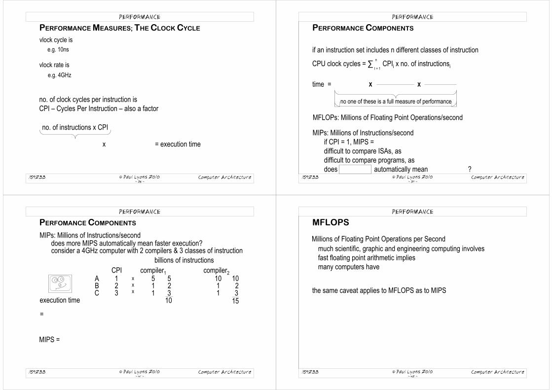
PERFORMANCE COMPONENTS
PERFORMANCE
time =
CPU clock cycles = ∑ CPIi x no. of instructionsiI = 1
n
if an instruction set includes n different classes of instruction
MFLOPs: Millions of Floating Point Operations/second
MIPs: Millions of Instructions/secondif CPI = 1, MIPS =difficult to compare ISAs, as difficult to compare programs, as does automatically mean ?
x x
no one of these is a full measure of performance
x x
© Paul Lyons 2010~ 41 ~
159233 Computer Architecture
PERFOMANCE COMPONENTS
PERFORMANCE
MIPs: Millions of Instructions/seconddoes more MIPS automatically mean faster execution?consider a 4GHz computer
billions of instructions
compiler1ABC
51 1
compiler210
1 1execution time
=
& 3 classes of instructionwith 2 compilers
MIPS =
CPI123
xxx
52310
102315
© Paul Lyons 2010~ 42 ~
159233 Computer Architecture
MFLOPS
PERFORMANCE
Millions of Floating Point Operations per Second
much scientific, graphic and engineering computing involvesfast floating point arithmetic implies many computers have
the same caveat applies to MFLOPS as to MIPS

© Paul Lyons 2010~ 43 ~
159233 Computer Architecture
BENCHMARKS
PERFORMANCE
too many variables, too much hype
benchmarks are standard programs whose e.g. Livermore loops
e.g. SPEC benchmark suites
manufacturers can to achieve good statsgives an unrealistic impression of
© Paul Lyons 2010~ 44 ~
159233 Computer Architecture
PARALLELISM
PERFORMANCE
some tasks can besystems that can be divided intoe.g. the atmosphere (weather prediction)
Pprocessors
ideallyin practice,
can't be eliminated
© Paul Lyons 2010~ 45 ~
159233 Computer Architecture
PARALLELISM –AMDAHL'S LAWPARALLELISM
PERFORMANCE
how do we measure ?
if a task takes 100s in one configuration and 80s in another, what's the speedup?speed1 = 1 task/100s =speed2 = 1 task/80s =speedup = 0.0125 / 0.01 =
T
ts tP
max speedup �
=
if we have P processors working perfectly in parallel then we reduce the time for the parallel section of the code by a factor of P so the total task time in the parallel configuration TP =speedup S =
most code is a mixture ofserial processing component is & limits
if tp can be reduced to 0
© Paul Lyons 2010~ 46 ~
159233 Computer Architecture
PARALLELISM - AMDAHL'S LAWPARALLELISM
PERFORMANCE
parallelism has two flavoursindependent tasks;dependant tasks;
many tasks in computers involve cf. assembly line for producing goods that undergo same operation sequence
A1 B1 C1
A2 B2 C2
A3 B3 C3

© Paul Lyons 2010~ 47 ~
159233 Computer Architecture
PIPELINE PERFORMANCE
PERFORMANCE
if each task in a pipeline of length L takes t secondssingle task takes
but for n tasks delay before 1st output =delay between subsequent outputs =T(n) =
= (L + n - 1)t
1 2 L
t t t+ + +
© Paul Lyons 2010~ 48 ~
159233 Computer Architecture
PIPELINE
PERFORMANCE
pipeline characteristics
pipeline rate, r∞ =pipeline startup time, s =half performance vector length, n½
(L-1)t + n½ t =n½ =
=
© Paul Lyons 2010~ 49 ~
159233 Computer Architecture
NUMBERS AND THE DATAPATH
COMPUTER ARITHMETIC
datapathALU
number representation2's complement
arithmetic operations+, *, /, shift
© Paul Lyons 2010~ 50 ~
159233 Computer Architecture
2's COMPLEMENT
COMPUTER ARITHMETIC
used in nearly all microprocessorsmost significant bit
other bits

© Paul Lyons 2010~ 51 ~
159233 Computer Architecture
INTEGERS AND ADDRESSES
COPMPUTER ARITHMETIC
integers are , addresses are
Note: unsigned addresses are not used in all computerstransputer addresses are 2's complement, in the range -231 to 231-1
no type information included with the data
© Paul Lyons 2010~ 52 ~
159233 Computer Architecture
2's COMPLEMENT
COMPUTER ARITHMETIC
for n bit numbers2n-1 positive numbers, starting at 02n-1 negative numbers, starting at -1|max –ve no| =x + -x =-x =-2n-1
operation overflows
0
0000 1
0001 2
0010
3
0011
4
0100
5
01016
01107
0111
-8
1000
-7
1001
-6
1010
-5
1011
-4
1100
-3
1101
-2
1110
-1
1111
A
101111000111
101111011000
-5-3-8
-5-4-8
0001101
00011011111111111111111111111111
1
© Paul Lyons 2010~ 53 ~
159233 Computer Architecture
OVERFLOW DETECTION
COMPUTER ARITHMETIC
easy to detect: when
on overflow address of overflowing instruction savedinterrupt handler is called andafter interrupt code finishes, instruction
© Paul Lyons 2010~ 54 ~
159233 Computer Architecture
1-BIT ALU
BUILDING UP THE DATAPATH
bit-slice architecturedesign an ALU component that handles
logical operations require cin
a0
b0
result0
a1
b1
result1
a31
b31
result31
operation
We could extend this design by adding more functional blocks, e.g. multipliers
carry propagation carry lookahead
ab
c
∑
cout
operation
result
invertb
invertb

© Paul Lyons 2010~ 55 ~
159233 Computer Architecture
can we detect when less significant bit slices will generate a carry output?set up modules that allow modules generally incorporate
1-BIT ALU – ADDING CARRY LOOKAHEAD1-BIT ALU
BUILDING UP THE DATAPATH
conventional full adder involves we could design a 32-bit adder as
64 inputs � 264 terms; too bigis there a less expensive way?
© Paul Lyons 2010~ 56 ~
159233 Computer Architecture
1-BIT ALU – ADDING CARRY LOOKAHEAD1-BIT ALU
BUILDING UP THE DATAPATH
a b cin cout sum0 0 0 0 00 0 1 0 1
0 1 0 0 10 1 1 1 01 0 0 0 11 0 1 1 0
1 1 0 1 01 1 1 1 1
cout always 0: carry kill
cout =cin: carry propagate
cout =1: carry generate
Gi =Pi =carry input to the next phase:ci+1 =similarly:ci = substituting repeatedly:ci+1 =
c1+1 ==
Boolean expressions for G, and P, :
all can be calculated in parallel from data inputs and c0
© Paul Lyons 2010~ 57 ~
159233 Computer Architecture
1-BIT ALU – ADDING CARRY LOOKAHEAD
BUILDING UP THE DATAPATH
carry lookahead circuit works onCL units are usually associated with
cascaded to make up
ALU
CL
CL
CL
CL
CL
CL
CL
CL
CL
CL
CL
CL
CL
CL
CL
© Paul Lyons 2010~ 58 ~
159233 Computer Architecture
1-BIT ALU – OTHER OPERATIONS
BUILDING UP THE DATAPATH
logical operationse.g. ANDbit-for-bit logical operation on a pair of words
shift operations e.g. sll & srl (Shift Left Logical & Shift Right Logical)shift information in a register by a specified no. of bits
combination of logical and shift operations to extract parts of a wordcreate a 32-bit mask with desired bits set to 1 (e.g. 8 bits for a character)AND andshift result by

© Paul Lyons 2010~ 59 ~
159233 Computer Architecture
1-BIT ALU – OVERFLOW DETECTION
BUILDING UP THE DATAPATH
when overflow occurs, carry-in and carry-out of sign bit differ connect an EOR gat to cin and cout of most significant adder
cin
a0
b0
result0
a1
b1
result1
a31
b31
result31
operation
overflow
invertb
© Paul Lyons 2010~ 60 ~
159233 Computer Architecture
1-BIT ALU - SLT
BUILDING UP THE DATAPATH
result = ;
if a < b , is equivalent to
set invertb when performing slt operation to-ve values have a sign bitfeed o/p of back tomake the o/p MUX in all the ALUs
ab
c
∑
cout
operation
result
ALU31
ab
c
∑
cout
operation
result
ALU0
0
operation01223
invertb--011
andoraddsubslt
invertbinvertb
© Paul Lyons 2010~ 61 ~
159233 Computer Architecture
BRANCH INSTRUCTIONS –BEQ AND BNE
BUILDING UP THE DATAPATH
equality test for beq and bne instructions also relies onif a=b, then
operation0122
invertb--01
andoraddsubslt 3 1
zero-detect circuit controls
bne 2 1beq 2 1
bne and beq also use
coupled with invertb
need to connect to32-input active-low-input AND gate (i.e., a NOR gate)
© Paul Lyons 2010~ 62 ~
159233 Computer Architecture
SHIFT
BUILDING UP THE DATAPATH
5-bit shamt field specifiestoo slow to shift in
barrel shifter shiftse.g. to shift 5 bits, shamt is
1's bit 4's bit2's bit2's bit

© Paul Lyons 2010~ 63 ~
159233 Computer Architecture
control
DATAPATH LAYOUT
BUILDING UP THE DATAPATH
registers ALU
instruction decoding
bit 0
bit 31
register decoding
data
ALU layout is very regular layout on silicon is also highly structuredcontrol flows and data flows are orthogonal minimises complexity and communication times
© Paul Lyons 2010~ 64 ~
159233 Computer Architecture
MULTIPLIER
BUILDING UP THE DATAPATH
signed multiplication
+
problem:takes multiple clock cycles
© Paul Lyons 2010~ 65 ~
159233 Computer Architecture
MULTIPLIER - FASTER
BUILDING UP THE DATAPATH
∑ ∑ ∑ ∑ ∑ ∑ ∑
∑ ∑ ∑ ∑ ∑ ∑ ∑
∑ ∑ ∑ ∑ ∑ ∑ ∑
multiplier
multiplicand 0101
x1101
0101
0000
0101
0101
1000001
01100101
multiplicand
01100101
multiplier
what if we put an adderafter each partial product?(except the first, of course)
∑ ∑ ∑ ∑ ∑ ∑ ∑
∑ ∑ ∑ ∑ ∑ ∑ ∑
∑ ∑ ∑ ∑ ∑ ∑ ∑
∑ ∑ ∑ ∑ ∑ ∑ ∑
∑∑∑∑∑∑∑
this architecture is wellsuited to
∑
∑
∑
© Paul Lyons 2010~ 66 ~
159233 Computer Architecture
BOOTH'S ALGORITHM WORKS FOR 2's COMP. NUMBERS
BUILDING UP THE DATAPATH
Booth noticed that, when counting in binary,a string of
will be with a next time the
so the string of can be rewrittenas instead of
2m bit
2n bit
…011111…
…10000-1…
…100000…
what's the benefit of that?a simple multiplier uses to multiply by string of x 1sbut if the multiplier can handle , �
the algorithm looking for00 – string of zeros;10 – start of a string of 1s;11 – middle of string of zeros;01 – end of a string of zeros;
=
still have to

© Paul Lyons 2010~ 67 ~
159233 Computer Architecture
MIPSMULTIPLICATION
BUILDING UP THE DATAPATH
the product of a 32-bit multiplications mult and multu occupies 64 bits
hi lo
hi and lo registers are not
mflo $1 (move from lo) putsmfhi $1 (move from hi) to check that
mult ASM instruction is a
generatesgenerates
© Paul Lyons 2010~ 68 ~
159233 Computer Architecture
DIVISION
BUILDING UP THE DATAPATH
mathematically (ideally), division is the inverse of multiplication
if a = b/cthen b =and if b = 1then
but with finite precision arithmetic, occur
© Paul Lyons 2010~ 69 ~
159233 Computer Architecture
DIVISION BY REPEATED SUBTRACTION
BUILDING UP THE DATAPATH
when we multiplied m by n to produce a product pwe generated
when we divide p by mwe're finding out
we can divide p by mby repeatedly p till
© Paul Lyons 2010~ 70 ~
159233 Computer Architecture
WHY ARE FPNUMBERS SPECIAL?
FLOATING POINT NUMBERS
we need a way to representnumbers with fractions, e.g. 3.14159very small numbers, e.g., 0.0000000001very large numbers, e.g. 178478 x 109
representation:sign, exponent, significand:more bits for mantissa �
more bits for exponent �
IEEE 754 floating point standard:single precision usesdouble precision uses

© Paul Lyons 2010~ 71 ~
159233 Computer Architecture
IEEE 754 FLOATING POINT STANDARD:
FLOATING POINT NUMBERS
msb of mantissa is , so only is stored
exponent is "biased" to make sorting easiersubtract 127 to get exponent for single precision & 1023 for double precision
mantissa(23 bits)
23 031
exponent(8 bits)
0
exponent(11 bits)
mantissa(52 bits)
single
double
5263
© Paul Lyons 2010~ 72 ~
159233 Computer Architecture
IEEE 754 FLOATING POINT STANDARD:
FLOATING POINT NUMBERS
special cases:
mantissaexponent
all 0s denormalised numbers; zero is a denormalised no. with
all 1s
all 0s ∞
non-0 NAN
QuietNAN has
SignalllingNAN has
rounding options:to nearest integer, to nearest even integer if fraction is exactly 0.5towards 0towards + ∞towards -∞
© Paul Lyons 2010~ 73 ~
159233 Computer Architecture
GUARD AND ROUND BITS
FLOATING POINT NUMBERS
consider adding two decimal numbers with 3 bits of precision 2.56 + 2.34 x 10²
2.34000.0256
2.340.02
2.3400.025
with noextra digits
with 1extra digit
with 2extra digits
extra bits
© Paul Lyons 2010~ 74 ~
159233 Computer Architecture
FLOATING POINT ADDITION
FLOATING POINT NUMBERS
align radix pointsdenormalise one number to
add mantissae
renormalise the resultwatch out for
round to correct number of significant digitsthis may occasionally ripple through to the msb and generate an unnormalised result
renormalise again if required

© Paul Lyons 2010~ 75 ~
159233 Computer Architecture
THE "STICKY BIT"
FLOATING POINT NUMBERS
When generating a result, a string of 0s may be followed by a 1 that will be normalised away
1.93650001 (ignoring the exponent)
simple rounding to nearest even value based on rounding digit, would produce
1.93650001
keep sticky bit as next bit to help resolve "mid-way" rounding problems
1
© Paul Lyons 2010~ 76 ~
159233 Computer Architecture
FLOATING POINT MULTIPLICATION
FLOATING POINT NUMBERS
add exponentsboth include a bias, so have to subtract 1 bias from the result
multiply
normalise result, check for overflow
round
renormalise if necessary
© Paul Lyons 2010~ 77 ~
159233 Computer Architecture
FLOATING POINT AND MIPS
FLOATING POINT NUMBERS
MIPS instructions to support IEEE single and double precision floating point:
add.s and add.d
sub.s and sub.d
mul.s and mul.d
div.s and div.d
c.<x>.s and c.<x>.d <x> may be eq, neq, lt, le, gt, ge
bclt and bclf
comparison sets bit to
single and double
© Paul Lyons 2010~ 78 ~
159233 Computer Architecture
ASMs (Designing a Controller)
COMPUTER PROCESSORS
ControllerASM
Architecture
Controller executes an infinite loop
• instructs processor to get an instruction from memory• identifies instruction that the processor has retrieved• instructs processor to perform data manipulations required by the instruction
Specifies timing of data manipulations
Receives status
information
Algorithmic State Machine

© Paul Lyons 2010~ 79 ~
159233 Computer Architecture
ASMs (Designing a Controller)
STATUS INFORMATION (architecture → controller)
Current instructionIf instruction involves a choice
e.g. JPZ instruction
then controller examines a status line to determine appropriate action
Other status signals are commonly usedNEG OVFL
© Paul Lyons 2010~ 80 ~
159233 Computer Architecture
ASMs (Designing a Controller)
CONTROL SIGNALS (controller → architecure)
Architectural
building block
Control commands No of bits
Registers
MUXes
Memory
etc
© Paul Lyons 2010~ 81 ~
159233 Computer Architecture
ASMs (Designing a Controller)
FINITE STATE MACHINES
0
- THE BASIS OF ALGORITHMIC STATE MACHINES
Rectangles contain
Diamonds containRoundtangles contain
P
Q R SZT F
© Paul Lyons 2010~ 82 ~
159233 Computer Architecture
Outputs in a are TRUE
ASMs (Designing a Controller)
A □ must be present
even if it is empty
A state specifies actions that occur on one clock pulse
Outputs in a □ are TRUE
during that state’s clock pulse, if …
P
RZ F

© Paul Lyons 2010~ 83 ~
159233 Computer Architecture
ASMs (Designing a Controller)
P
Q R SZT F
The state is represented as a numberAt any instant (clock pulse), the ASM
hasassertsasserts
if the condition that governs them is fulfilledASM calculates the
0
1 2
© Paul Lyons 2010~ 84 ~
159233 Computer Architecture
Specs for circuit to navigate round the state chart:
inputs output
No. of present stateStatus inputs
Any external inputsNext state no.
ASMs (Designing a Controller)
P
Q R SZT F
0
1 2
© Paul Lyons 2010~ 85 ~
159233 Computer Architecture
.
ASMs (Designing a Controller)
Z?
present state?
1 → next state
Next state no. ↓
present state no
TRUE → R2 → next state
TRUE → Q0 → next state
TRUE → S0 → next state
TRUE → P
P
Q R SZT F
0
1 2
repeat 0T
F
1
2
© Paul Lyons 2010~ 86 ~
159233 Computer Architecture
ASMs (Designing a Controller)
Ap Bp Z An Bn
The ASM state transition table (navigation only)
Inputs Outputs
P
Q R SZT F
0
1 2

© Paul Lyons 2010~ 87 ~
159233 Computer Architecture
ASMs (Designing a Controller)
General structure of the circuit
Combinatorial logic
Register
Outputs
Next state
Present
state
Status
Externalinputs
clock
P
Q R SZT F
0
1 2
© Paul Lyons 2010~ 90 ~
159233 Computer Architecture
1 00 10 00 0 Ap Bp
The complete ASM state transition table
Ap Bp Z
0 0 00 0 10 1 -1 0 -
An Bn
Inputs Outputs
P Q R S
ASMs (Designing a Controller)
clock
2-bit reg
Q1 Q0
D0
D1
Z
An
Bn
PQRS
P
Q R SZT F
0
1 2
© Paul Lyons 2010~ 91 ~
159233 Computer Architecture
ASMs (Designing a Controller)
A practical problem:initialising the state register
On automatic?
00
Found?
Fire
10Yes
Seek enemy target
01T
F
Consider a 22” naval gun• controlled by an ASM • autoseeking• autofiring
No
At power-up, if state register contains 0, 1, or 3if state register contains 2
√√√√?
© Paul Lyons 2010~ 92 ~
159233 Computer Architecture
ASMs (Designing a Controller)
On automatic?
00
Found?
Fire
10Yes
Seek enemy target
01T
F
No
We need a reset-on-powerup circuit
+5V
0V
rst
+5V
T
V
A practical problem:initialising the state register
Consider a 22” naval gun• controlled by an ASM • autoseeking• autofiring
At power-up, if state register contains 0, 1, or 3if state register contains 2

© Paul Lyons 2010~ 93 ~
159233 Computer Architecture
ASMs (Designing a Controller)
SUMMARY: DESIGNING AN ASM
Construct Shows all inputs and control signals
Translateexternal inputs (if any)status inputspresent statecontrol commandsnext state
Translate
© Paul Lyons 2010~ 94 ~
159233 Computer Architecture
but would you ever use an ASM instead of computer program?
ASMs underlie processor instruction sets
ASM vs. SOFTWARE
Software ASMsin discrete logic
ASMsin FPGA
.. .. ..
DQ
DQ
ASMs (Designing a Controller)
© Paul Lyons 2010~ 95 ~
159233 Computer Architecture
ASMs (Designing a Controller)
Is it easy to understand or modify an ASM circuit?
General format is easily recognisable
inputs commands
But combinatorial circuitry and high-level flowchart vocabularies differ significantly
© Paul Lyons 2010~ 96 ~
159233 Computer Architecture
ASMs (Designing a Controller)
Modifications to state sequence require a complete redesign
Disjunction between ASM diagram and combinatorial circuitry
Could the circuitry(and the outputs)
Is it easy to understand or modify an ASM circuit?

© Paul Lyons 2010~ 97 ~
159233 Computer Architecture
ASMs (Designing a Controller)
If we connect:the control input of a MUX to the state numberthe data inputs to TRUE and FALSE
We’ll use 1 MUX for each output (including the bits of the next state number)
state Q01234567
10010111
T F
.
01234567
Q
USING MUXES AS A LOOKUP TABLE
© Paul Lyons 2010~ 98 ~
159233 Computer Architecture
ASMs (Designing a Controller)
Outputs are sometimes
Q
11
A.B
T F
State no.
01234567
Q
A B
Simpler and easier to understand than completely combinatorial system
USING MUXES AS A LOOKUP TABLE
Q should be in state 3, if
© Paul Lyons 2010~ 99 ~
159233 Computer Architecture
ASMs (Designing a Controller)
USING MUXES AS A LOOKUP TABLE
Consider our prototype ASM
P
Q R SZT F
0
1 2
Ap Bp Z
0 0 00 0 10 1 -1 0 -
An Bn
1 00 10 00 0
Inputs Outputs
P Q R S
1 011 0 00 1 00
00
000 1
ZT F
0123
An
0123
Bn
D1
D0
Q1
Q0
0123
S
0123
R
P0123
0123
Q
© Paul Lyons 2010~ 100 ~
159233 Computer Architecture
ASMs (Designing a Controller)
A LIFT CONTROLLER

© Paul Lyons 2010~ 101 ~
159233 Computer Architecture
A LIFT CONTROLLER
ASMs (Designing a Controller)
© Paul Lyons 2010~ 102 ~
159233 Computer Architecture
A LIFT CONTROLLER
ASMs (Designing a Controller)
© Paul Lyons 2010~ 103 ~
159233 Computer Architecture
ASMs (Designing a Controller)
A LIFT CONTROLLER
© Paul Lyons 2010~ 104 ~
159233 Computer Architecture
ASMs (Designing a Controller)
A LIFT CONTROLLER

© Paul Lyons 2010~ 106 ~
159233 Computer Architecture
ASMs (Designing a Controller)
Up button means “Take something upstairs”
Down button means “Take something downstairs”
If the lift is downstairs,
If the lift is upstairs,
A LIFT CONTROLLER
© Paul Lyons 2010~ 107 ~
159233 Computer Architecture
ASMs (Designing a Controller)
door open?openDoor
upButton +
downButton?
N
Y
N
Y
closed?closeDoorN
000 (At bottom)
001 (Starting up)
up?
ResetUpRequest
010 (Going up)
goUpN
upButton +
downButton?Y
N
closed?
100 (Starting down)
closeDoorN
down?
ResetDnRequest
101 (Going down)
goDownNY
door open?
011 (At top)
Y
openDoorN
A LIFT CONTROLLER
© Paul Lyons 2010~ 110 ~
159233 Computer Architecture
ASMs (Designing a Controller)
AP BP CP AN BN CNcondition closeDoor
openDoor
resetUpRequest
resetDownRequest
goUp
goDown
0 0 0
0 0 1
0 1 0
0 1 1
1 0 0
1 0 1
cond1 = doorOpen . ~(upButton + downButton)cond2 = doorOpen . (upButton + downButton)
A LIFT CONTROLLER
© Paul Lyons 2010~ 111 ~
159233 Computer Architecture
ASMs (Designing a Controller)
D2
D1
D0Q0-Q3
openDoor
resetUpRequest
goDown
goUp
CN
clos
ed
DO UBDBT F up dow
n
closeDoor
AN
BN
resetDownRequest

© Paul Lyons 2010~ 112 ~
159233 Computer Architecture
ASMs (Designing a Controller)
Phase 1
Phase 2
A MULTIPLICATION CIRCUIT
© Paul Lyons 2010~ 113 ~
159233 Computer Architecture
ASMs (Designing a Controller)
How does “manual” multiplication work?
e.g. 510 x 11100101 Multiplicand
X 1011 Multiplier
0101
0101
0000
0101000
0110111
Partial products
Product
Hardware multiplication works similarlyBut multiplier
When the process ends, running total containsOtherwise we’d have to use
(=5510)
: AnalysisA MULTIPLICATION CIRCUIT
© Paul Lyons 2010~ 114 ~
159233 Computer Architecture
Partial products
ASMs (Designing a Controller)
0101 Multiplicand
X 1011 Multiplier
0101
0101
0000
0101000
0110111
Storage requirementsMultiplier Multiplicand Product
: AnalysisA MULTIPLICATION CIRCUIT
Product (=5510)
How does “manual” multiplication work?
e.g. 510 x 1110
© Paul Lyons 2010~ 115 ~
159233 Computer Architecture
0101
ASMs (Designing a Controller)
: Analysis
For each 1 in multiplier,addallowing for
1011
1 bit
2 bit
4 bit
8 bit
Each time a partial product is added to the running totalsignificance needs to beFirst PP goes into position withShift running total
Put running total in
A MULTIPLICATION CIRCUIT
0101

© Paul Lyons 2010~ 122 ~
159233 Computer Architecture
0110111
ASMs (Designing a Controller)
: Analysis
For each 1 in multiplier,add multiplicand into running totalallowing for significance of the 1 bit in the multiplier
1011
1 bit
2 bit
4 bit
8 bit
Each time a partial product is added to the running totalsignificance needs to beFirst PP goes into positionShift running total
Put running total in a shift register 2n bits wide
A MULTIPLICATION CIRCUIT
If multiplicand is large, Add an extra bit to the most significant shift register
+ 1
^
© Paul Lyons 2010~ 123 ~
159233 Computer Architecture
ASMs (Designing a Controller)
: Design of the architecture
SRA SRB
register
adder
A MULTIPLICATION CIRCUIT
© Paul Lyons 2010~ 124 ~
159233 Computer Architecture
0
SRA SRB
resetA resetBshiftA shiftB
loadMultiplier
multiplier
loadProduct
clock
register
multiplicand
loadMultiplicand
adder
Top 1/2 Bottom 1/2
lobit
Informal algorithm
Load
Load
Repeat 4 timesIf lowest bit of multiplier is , then
addShift and
ASMs (Designing a Controller)
A MULTIPLICATION CIRCUIT
© Paul Lyons 2010~ 125 ~
159233 Computer Architecture
incr
lobit?
eqz?
done
loadProductT
shiftAshiftB
F
F
00
01
11
10
Start? F
AP BP AN BN loadM
ultiplier
loadM
ultiplicand
clearCounter
reset A
increment
loadProduct
shift A
shift B
done
condition
0 0startT T T T0 1start
0 0
1 0 Tlobit
1 1 Tlobit
0 1
1 1 T-1 0
0 1 T Teqz
0 0 Teqz T T
1 1
ASMs (Designing a Controller)
AMULTIPLICATION CIRCUIT –ASM DIAGRAM
loadMultiplierloadMultiplicand
clearCounterresetA

© Paul Lyons 2010~ 126 ~
159233 Computer Architecture
AP BP AN BN loadM
ultiplier
loadM
ultiplicand
clearCounter
reset A
increment
loadProduct
shift A
shift B
done
condition
0 0startT T T T0 1start
0 0
1 0 Tlobit
1 1 Tlobit
0 1
1 1 T-1 0
0 1 T Teqz
0 0 Teqz T T
1 1
ASMs (Designing a Controller)
© Paul Lyons 2010~ 127 ~
159233 Computer Architecture
ASMs (Designing a Controller)
AP BP AN BN loadM
ultiplier
loadM
ultiplicand
clearCounter
reset A
increment
loadProduct
shift A
shift B
done
condition
0 0startT T T T0 1start
0 0
1 0 Tlobit
1 1 Tlobit
0 1
1 1 T-1 0
0 1 T Teqz
0 0 Teqz T T
1 1
D1
D0
Q1
Q0
0123
AN
0123
BN
AP
BP
T F eqz
lobit
start
0123
loadMultiplierloadMultiplicandClearCounterResetA
0123
increment
0123
loadProduct
0123
shiftAshiftB
0123
done
Q0Q1
clearCounter
increment
eqz
© Paul Lyons 2010~ 128 ~
159233 Computer Architecture
THE PROCESSOR =DATAPATH +CONTROL
SINGLE-CYCLE ARCHITECTURE
datapath can process data as specified in the instructions
but fetch/decode/execute cycle needs
control signals regulatetradeoffs between complex processing and fast hardware moduleswant to minimise both
control loop always has•output to determine the location of the next instruction •read specified by the instruction (sometimes 1, sometimes 2)•perform (memory ref, arithmetic/logical, or branch)
© Paul Lyons 2010~ 129 ~
159233 Computer Architecture
THE ARCHITECTURE
SINGLE-CYCLE ARCHITECTURE
PC
registers
instructionmemory
data memory
data out
data in
ALU

© Paul Lyons 2010~ 130 ~
159233 Computer Architecture
COMBINATORIAL vs. SEQUENTIAL LOGIC
SINGLE-CYCLE ARCHITECTURE
datapath components developed so far useoutputsoutput of a given set of inputsdelay between
full datapath iscontains storage elementsoutputs depend onclock regulates
controller is a sequential circuitusually implemented as
© Paul Lyons 2010~ 131 ~
159233 Computer Architecture
CLOCKING DATA THROUGH APATH
SINGLE-CYCLE ARCHITECTURE
storage(sequential)
storage(sequential)
datapath component(combinatorial)
datapath component(combinatorial)
clock
nc > (n+1)(c-δc)(n+1)δc > c
Xsetup
holdregister loads dataregister o/p unstableregister i/p must be stableregister o/p stable duringcycle time = +
is it worth cutting a slow stage into two?
yes, if:
© Paul Lyons 2010~ 132 ~
159233 Computer Architecture
GATED CLOCKS
SINGLE-CYCLE ARCHITECTURE
we don't always want to load data on every clock cycleuse a separate write control line toclock edge specifies the data should be loadedwrite line specifies the data should be loaded
clockwrite write
© Paul Lyons 2010~ 133 ~
159233 Computer Architecture
INSTUCTION SUBSET
SINGLE-CYCLE ARCHITECTURE
memory reference instructions lw and swarithmetic instructions add, sub, and, or, sltbranch instructions beq and j
two phases single-cycle implementation, combinatorial controllermulti-cycle implementation – leads to

© Paul Lyons 2010~ 134 ~
159233 Computer Architecture
THE PROGRAM COUNTER
SINGLE-CYCLE ARCHITECTURE
add
4
PCinstructionmemory
instruction
© Paul Lyons 2010~ 135 ~
159233 Computer Architecture
REGISTER FILE ANDR-FORMAT INSTRUCTIONS
SINGLE-CYCLE ARCHITECTURE
register file contains 32 32-bit registersimplemented as a fast static RAM with dedicated read and write portsaddresses correspond tocontrol signals, based on current instruction, specifyallows two reads and 1 write on a clock cycleALU operates on output from 2 registers, writes result back to register file
write register
read register1read register2
read data1
read data2
write data
/
/
/
5
5
5
instruction regWrite
ALU
zero
4
ALUoperation
© Paul Lyons 2010~ 136 ~
159233 Computer Architecture
MEMORY REFERENCES
SINGLE-CYCLE ARCHITECTURE
lw
sw$t1, offset ($t2)
16-bit value to add to $t2
to generate branch destinationdedicated ALU adds offset toif offset is –ve, sign is in bit 15need to (set bits 16 - 31 to 1)
instruction
read data1
read data2
write register
read register1read register2
write data
regWrite
/
/
/
5
5
5
zero
ALU
ALUoperation
4
sign-extend
data memory
read write
read address
write address
16 32
© Paul Lyons 2010~ 138 ~
159233 Computer Architecture
THE BEQCONTROL LOGIC
SINGLE-CYCLE ARCHITECTURE
branch destinationALU
sum
shiftleft 2
pc+4
branch address is register (PC) + offsetPC + 4 (here the units are bytes!) isoffset is ; needsunit of offset is words, not bytes; shift it 2 bits to the left to multiply by 4
signextend
instruction
beq $1, $2, offset

© Paul Lyons 2010~ 139 ~
159233 Computer Architecture
SINGLE-CYCLE ARCHITECTURE
sum
4
shift left 2
PCsum
sign-extendinstruction 0:15
instructionmemory
branchdestination
ALUsum
© Paul Lyons 2010~ 140 ~
159233 Computer Architecture
THE BEQCONTROL LOGIC
SINGLE-CYCLE ARCHITECTURE
branch destinationALU
sum
shiftleft 2
pc+4
signextend
instruction
beq is a conditional branch instructionso processor mustALUif ALU's zero-detect is TRUE,
zero to branch control logic
regWrite
addread data1
read data2write register
read register1read register2
write data
operation
© Paul Lyons 2010~ 141 ~
159233 Computer Architecture
THE J INSTRUCTION
SINGLE-CYCLE ARCHITECTURE
j address
another instruction that loads the PC – unconditionally this time26 bit address has 2 0 bits added tono negative addresses, so no need fortop 4 bits of PC are left unaffectedso j instruction can only access
instructionmemory
PC
26unchanged
00
© Paul Lyons 2010~ 142 ~
159233 Computer Architecture
SINGLE CLOCK CYCLE RESTRICTIONS
SINGLE-CYCLE ARCHITECTURE
all operations must start and finish in in 1 clock cycleno resources can be sharedmultiple operations require
increment PC, calculate address, compare registers all need
however, different instruction types can use the same resourcememory references calculateregister operations calculatecan multiplex
instruction
read data1
read data2
write register
read register1read register2
write data
regWrite
/
/
/
5
5
5
zero
ALU
ALUoperation
4
sign-extend16 32
data memory
read write
read adddress
write adddress
similarly

© Paul Lyons 2010~ 143 ~
159233 Computer Architecture
ADDING INSTRUCTION MEMORY
SINGLE-CYCLE ARCHITECTURE
instruction
read data1
read data2
write register
read register1read register2
write data
regWrite
/
/
/
5
5
5
zero
ALU
ALUoperation
4
sign-extend16 32
data memory
read write
read adddress
write adddress
instructionmemory
sumPC
4
Single-cycle instruction requires separate data and instruction memoryno time to read
© Paul Lyons 2010~ 144 ~
159233 Computer Architecture
instruction
read data1
write register
read register1read register2
write data
regWrite
zero
ALU
ALUoperation
4
ADDING THE BEQ INSTRUCTION
SINGLE-CYCLE ARCHITECTURE
data memory
read write
read adddress
write adddress
sign-extend
read data2
sum
4
shift left 2
PC
instructionmemory
sum
© Paul Lyons 2010~ 145 ~
159233 Computer Architecture
SINGLE-CYCLE ARCHITECTURE
write register
read register1read register2write data read data2
read data1
ALU zero
data memory
read adddress
write adddress
instruc-tion
memory
11:15
16:20
21:25
sum
PC
4
sign-extend
0:15 shiftleft 2
sum
© Paul Lyons 2010~ 146 ~
159233 Computer Architecture
ALUCONTROL
SINGLE-CYCLE ARCHITECTURE
controller will handle a subset of the ALU functions
functionandoraddsub
set on less than
ALU Control Input000001010110111

© Paul Lyons 2010~ 147 ~
159233 Computer Architecture
COMBINATORIAL CONTROL UNIT
SINGLE-CYCLE ARCHITECTURE
instructionlwswbeqaddsubandorslt
ALUop0000011010101010
ALU actionaddadd
subtractadd
subtractandor
set on less than
function codexxxxxxxxxxxxxxxxxx100000100010100100100101101010
opcodelwswbeq
R-typeR-typeR-typeR-typeR-type
ALU control010010110010110000001111
A10011111
A00100000
F3--00001
F1--01001
F0--00010
C20101001
C11111001
C00000011
inputs outputs
6 bits 6 bitsF2--00110
© Paul Lyons 2010~ 148 ~
159233 Computer Architecture
COMBINATORIAL CONTROL UNIT
SINGLE-CYCLE ARCHITECTURE
A10011111
A00100000
F3--00001
F2--00110
F1--01001
F0--00010
C20101001
C11111001
C00000011
A10011111
A00100000
F3--00001
F2--00110
F1--01001
F0--00010
C20101001
C11111001
C00000011
© Paul Lyons 2010~ 149 ~
159233 Computer Architecture
COMBINATORIAL CONTROL UNIT
SINGLE-CYCLE ARCHITECTURE
A10011111
A00100000
F3--00001
F2--00110
F1--01001
F0--00010
C20101001
C11111001
C00000011
A1A0=00F3F2
F1F0 00 01 11 10
00
01
11
10
0 0 0 0
0 0 0 0
0 0 0 0
0 0 0 0
F3F2
F1F0 00 01 11 10
00
01
11
10
1 1 1 1
1 1 1 1
1 1 1 1
1 1 1 1
F3F2
F1F0 00 01 11 10
00
01
11
10
- - - -
- - - -
- - - -
- - - -
F3F2
F1F0 00 01 11 10
00
01
11
10
0 0 - -
- 0 - -
- - - -
1 - - 1
A1A0=01 A1A0=11 A1A0=10
C2 = A0C2 = A0 + A1F1C2 =
© Paul Lyons 2010~ 150 ~
159233 Computer Architecture
COMBINATORIAL CONTROL UNIT
SINGLE-CYCLE ARCHITECTURE
A10011111
A00100000
F3--00001
F2--00110
F1--01001
F0--00010
C20101001
C11111001
C00000011
C2 = A0 + A1F1
A1A0=00F3F2
F1F0 00 01 11 10
00
01
11
10
1 1 1 1
1 1 1 1
1 1 1 1
1 1 1 1
F3F2
F1F0 00 01 11 10
00
01
11
10
1 1 1 1
1 1 1 1
1 1 1 1
1 1 1 1
F3F2
F1F0 00 01 11 10
00
01
11
10
- - - -
- - - -
- - - -
- - - -
F3F2
F1F0 00 01 11 10
00
01
11
10
1 0 - -
- 0 - -
- - - -
1 - - 1
A1A0=01 A1A0=11 A1A0=10
C1 = `A1 + `F2C1 = `A1C1 =

© Paul Lyons 2010~ 151 ~
159233 Computer Architecture
C0 = A1F3 + A1F0C0 = A1F3
COMBINATORIAL CONTROL UNIT
SINGLE-CYCLE ARCHITECTURE
A10011111
A00100000
F3--00001
F2--00110
F1--01001
F0--00010
C20101001
C11111001
C00000011
C2 = A0 + A1F1
C1 = `A1 + `F2
A1A0=00F3F2
F1F0 00 01 11 10
00
01
11
10
0 0 0 0
0 0 0 0
0 0 0 0
0 0 0 0
F3F2
F1F0 00 01 11 10
00
01
11
10
0 0 0 0
0 0 0 0
0 0 0 0
0 0 0 0
F3F2
F1F0 00 01 11 10
00
01
11
10
- - - -
- - - -
- - - -
- - - -
F3F2
F1F0 00 01 11 10
00
01
11
10
0 0 - -
- 1 - -
- - - -
0 - - 1
A1A0=01 A1A0=11 A1A0=10
C0 =
© Paul Lyons 2010~ 152 ~
159233 Computer Architecture
COMBINATORIAL CONTROL UNIT
SINGLE-CYCLE ARCHITECTURE
C2 = A0 + A1F1
C1 = `A1 + `F2
C0 = A1F3 + A1F0
C2 = A0 + A1F1
C1 = `A1 + `F2
C0 = A1F3 + A1F0
© Paul Lyons 2010~ 153 ~
159233 Computer Architecture
C1 = `A1 + `F2
C0 = A1F3 + A1F0
C2 = A0 + A1F1
control block
SINGLE-CYCLE ARCHITECTURE
A
01
F
0123
1C
2
0
COMBINATORIAL CONTROL UNIT
© Paul Lyons 2010~ 154 ~
159233 Computer Architecture
zero16:20
21:25write register
read register1read register2write data read data2
read data1
ALU data memory
read adddress
write adddress
instruc-tion
memory 11:15
sum
PC
4sum
shiftleft 2
sign-extend0:15
THE CONTROL SIGNALS
SINGLE-CYCLE ARCHITECTURE
ALUop26:31
0:5 ALUControl
4
2 controllerMemToReg MemRead MemWritePCSrc RegDst RegWrite ALUSrc

© Paul Lyons 2010~ 155 ~
159233 Computer Architecture
CONTROLLER TRUTH TABLE
SINGLE-CYCLE ARCHITECTURE
instructionR-type
lwswbeq
( 0 )(35)(43)( 4 )
regdest10XX
ALUSrc0110
MemToReg01XX
RegWrite1100
MemRead0100
MemWrite0010
Branch0001
ALUOp1
1000
ALUOp2
0001
50110
40000
30010
20001
10110
00110
opcode
op5.`op4.`op3.`op2.op1.op0MemToReg =
`op5.`op4.`op3.`op2.`op1.`op0RegDest =
op5.`op4.`op3.`op2.op1.op0MemRead =
op5.`op4. op3.`op2.op1.op0MemWrite =
`op5.`op4.`op3. op2.`op1.`op0Branch =
`op5.`op4.`op3.`op2.`op1.`op0ALUOp1 =
`op5.`op4.`op3. op2.`op1.`op0ALUOp2 =
op5.`op4.`op3.`op2.op1.op0ALUSrc =+ op5.`op4. op3.`op2.op1.op0
`op5.`op4.`op3.`op2.`op1.`op0RegWrite =+ op5.`op4. op3.`op2.op1.op0
© Paul Lyons 2010~ 156 ~
159233 Computer Architecture
CONTROLLER
SINGLE-CYCLE ARCHITECTURE
op5.`op4.`op3.`op2.op1.op0MemToReg =
`op5.`op4.`op3.`op2.`op1.`op0RegDest =
op5.`op4.`op3.`op2.op1.op0MemRead =
op5.`op4. op3.`op2.op1.op0MemWrite =
`op5.`op4.`op3. op2.`op1.`op0Branch =
`op5.`op4.`op3.`op2.`op1.`op0ALUOp1 =
`op5.`op4.`op3. op2.`op1.`op0ALUOp2 =
op5.`op4.`op3.`op2.op1.op0ALUSrc =+ op5.`op4. op3.`op2.op1.op0
`op5.`op4.`op3.`op2.`op1.`op0RegWrite =+ op5.`op4. op3.`op2.op1.op0
Vcc
op5
op4
op3
op2
op1
op0
output node
© Paul Lyons 2010~ 157 ~
159233 Computer Architecture
CONTROLLER
SINGLE-CYCLE ARCHITECTURE
op5.`op4.`op3.`op2.op1.op0MemToReg =
`op5.`op4.`op3.`op2.`op1.`op0RegDest =
op5.`op4.`op3.`op2.op1.op0MemRead =
op5.`op4. op3.`op2.op1.op0MemWrite =
`op5.`op4.`op3. op2.`op1.`op0Branch =
`op5.`op4.`op3.`op2.`op1.`op0ALUOp1 =
`op5.`op4.`op3. op2.`op1.`op0ALUOp2 =
op5.`op4.`op3.`op2.op1.op0ALUSrc =+ op5.`op4. op3.`op2.op1.op0
`op5.`op4.`op3.`op2.`op1.`op0RegWrite =+ op5.`op4. op3.`op2.op1.op0
Vcc
op5
op4
op3
op2
op1
op0
© Paul Lyons 2010~ 159 ~
159233 Computer Architecture
SINGLE-CYCLE vs.MULTI-CYCLE IMPLEMENTATION
MULTI-CYCLE ARCHITECTURE
with single cycle, longest instruction limits speed of whole machine load instruction involvesCPI = 1 looks good, but
multi-cycle instructions would be faster for all but longest instructionsingle memory can be usedsingle ALU can be used for data, PC and address operations
load and store instructions involve1 memory access1 memory accessseparate and memories necessary to
we can divide instructions into phasese.g., instruction read; register(s) read; compute phase; register write (R-type instruction)set clock period to length of longest phase of an instruction instead of longest instructioninstructions become

© Paul Lyons 2010~ 160 ~
159233 Computer Architecture
TRISTATE OUTPUTS
MULTI-CYCLE ARCHITECTURE
using a multiplexor to select inputs to an ALU meansmultiple 32-bit-wide data paths
alternatively, run a single 32-bit bus past all the sourcesgive the sources tristate outputswith n data sources:
log n mux control inputs �
32 x n data wires �
© Paul Lyons 2010~ 161 ~
159233 Computer Architecture
DATAPATH
MULTI-CYCLE ARCHITECTURE
write signals required
no longer single clock cycle with standard sequence of control signals
temporary registers needed for results because:signal is computed on 1 clock cycle andinputs that produced it changeimplicit control signals used
4
memoryread adddress
write adddress
write data
PC
PCWrite
ALUSelA
RegDest
IRWrite
MemWrite
MemRead
0
1
2
3
instruction
register
memory data
register
ALUSelB
zeroALU
ALU
out
shiftleft 2
write registerread register1
write data
read data2
read data1
read register2
sign-extend
A
B
Memto Reg
I orD
A
B
ALU
out
© Paul Lyons 2010~ 162 ~
159233 Computer Architecture
BREAKING INSTRUCTION INTO CLOCK CYCLES
MULTI-CYCLE ARCHITECTURE
write registerread register1
write data
read data2
read data1
read register2instruction
registersign-extend shift
left 2
4
memoryread adddress
write adddress
write data
PC
zeroALU
PCWrite
MemRead
MemWrite
IRWrite
RegDest
ALUSelA
0
1
2
3
equalise time spent in each clock cycleminimise time for whole instruction
clock cycle should contain no more than111
memory data
register A
B
ALUSelB
ALU
out
Memto Reg
I orD
© Paul Lyons 2010~ 163 ~
159233 Computer Architecture
CLOCK CYCLE 1 - Instruction Fetch
MULTI-CYCLE ARCHITECTURE
common to all instructions
stores instruction in IR so that
load IR and incPC in parallelbothusetake effect
IR �
PC �

© Paul Lyons 2010~ 164 ~
159233 Computer Architecture
A �
B �
ALUout �
CLOCK CYCLE 2 – Instruction Decode & Register Fetch
MULTI-CYCLE ARCHITECTURE
read registers specified by rs and rt fields of instruction into A and B registersdon't need them for all instructions, but does no harm
also compute branch target address, just in casesave result
still don’t know what the instruction is, tho it's in the IR
© Paul Lyons 2010~ 165 ~
159233 Computer Architecture
CLOCK CYCLE 3 – Mem Addr Computation, or Branch Completion
MULTI-CYCLE ARCHITECTURE
in this clock cycle, depends on
memory reference instructions (lw and sw)ALUout �
R-type instructions (arithmetic-logic)ALUout �
conditional branch instructionsif (A==B) PC �
jump instructionPC �
© Paul Lyons 2010~ 166 ~
159233 Computer Architecture
CLOCK CYCLE 4 – Mem Access, or R-Type Instruction Completion
MULTI-CYCLE ARCHITECTURE
memory reference instructions (lw and sw)MDR �
ormemory[ALUout] �
R-type instructions (arithmetic-logic)reg [ IR [11:15 ]] �
© Paul Lyons 2010~ 167 ~
159233 Computer Architecture
CLOCK CYCLE 5 – Memory Read Completion
MULTI-CYCLE ARCHITECTURE
load instructionMDR �
ormemory[ALUout] �
P 329

© Paul Lyons 2010~ 168 ~
159233 Computer Architecture
Memory read completion
Memory accessor R-type
completion
Memory Address. Computation, or.
Branch Completion
R-type memory-reference branch jump
instr decode,register fetch
MULTI-CYCLE ARCHITECTURE
write registerread register1
write data
read data2
read data1
read register2instruction
registersign-extend shift
left 2
4
memoryread adddress
write adddress
write data
PC
zeroALU
PCWrite
MemRead
MemWrite
IRWrite
RegDest
ALUSelA
0
1
2
3
memory data
register A
B
ALUSelB
ALU
out
Memto Reg
I orD
instructionfetch
IR � memory[PC];PC � PC + 4;
A � reg[ IR [ 21:25 ]];B � reg[ IR [ 16:20 ]];
ALUout
� PC + (sign-extend( IR [0:15] ) << 2);
ALUout
� A op B;
reg[IR [11:15]]
�ALUout;
ALUout
� A + sign-extend(IR[0:15]);
MDR � M[ALUout] # sw
OR: M[ALUout] � B # lw
load: reg[IR [16:20]] � MDR;
if (A==B)PC � ALU
out;
PC � { PC[28:31] , IR[0:25], 2'b00 };
© Paul Lyons 2010~ 169 ~
159233 Computer Architecture
STATE MACHINE CONTROLLER
MULTI-CYCLE ARCHITECTURE
Standard ASM approach to constructing a controllersee Patterson & Hennessy, pps 330-340
© Paul Lyons 2010~ 170 ~
159233 Computer Architecture
MICROPROGRAMMING
MULTI-CYCLE ARCHITECTURE
look up control signals for (instruction, clock cycle) instead of calculating them
jump table2n entries
processorcontrol lines
microprogramcounter
0: jump to fetch
fetch
microprogram memory
instructionmicrocode
consider a processor with n-bit opcode and no instruction 0 on power-up, fetch loads with , jumps tojump table jumps to ; instruction executes, jumps back to
© Paul Lyons 2010~ 171 ~
159233 Computer Architecture
MICROPROGRAMMING
MULTI-CYCLE ARCHITECTURE
extra memory access for each clock cycle
new microcode can be downloaded

© Paul Lyons 2010~ 172 ~
159233 Computer Architecture
EXCEPTIONS AND INTERRUPTS
MULTI-CYCLE ARCHITECTURE
exceptions are unexpected eventse.g.
interrupts are unexpected events from outside the processorI/O devices generate interrupts to signal input events; process swapping
terminological confusionMIPS convention: both types of event areIntel 32-bit processor convention: both
handling exceptions is time-consumingmay determine overall speed of machinesave address of current instructiontransfer control tooperating system: OS can then or
© Paul Lyons 2010~ 173 ~
159233 Computer Architecture
EXCEPTIONS AND INTERRUPTS
MULTI-CYCLE ARCHITECTURE
vectored interruptswhen exception occurs, controllerOS routine to handle that exception is
exception handling startse.g. signals from:overflow detector, unrecognised opcode (simplified MIPS processor)external pin on processor (I/O devices)states in controller ASM where exceptions can occur have jump
ASM loads: cause register withEPC withPC with (location of OS routine for )
OS:handles
or
© Paul Lyons 2010~ 174 ~
159233 Computer Architecture
COMPLEX MULTI-CYCLE ARCHITECTURES
MULTI-CYCLE ARCHITECTURE
suitable forCISC machines can have instructions from 2-3 clock cycles to tens or even hundredswhen data for current instruction moves along datapath,early parts of datapath
© Paul Lyons 2010~ 175 ~
159233 Computer Architecture
THE BASIC IDEA
PIPELINING
multi-cycle architecture reducesinstructions stillbut some instructions take fewer thanso
can we combine 1 CPI behaviour with shorter clocks?
single-cycle (1 CPI) architecture simple but slowno instruction can run faster than the slowest
each stage in datapath acts on data from a separate instructionD enacts phase 4 of instruction i on data for instruction iC enacts phase 3 of instruction i-1 on data for instruction i-1later instructions can’t work on data currently being produced by the datapathresources can’t be used at several stages in the datapathneed intermediate registers to keep results available for several clock cycles
DCBA

© Paul Lyons 2010~ 176 ~
159233 Computer Architecture
COMPARISON OF APPROACHES
PIPELINING
Instruction Instr Fetch Reg Read ALU Op Data Mem Reg Write TotalR Format 10ns 5 ns 10ns 5ns 30ns
lw 10ns 5ns 10ns 10ns 5ns 40nssw 10ns 5ns 10ns 10ns 35nsbeq 10ns 5ns 10ns 25
10 20 30 40 50 60 70 80 900
pipeline cycleinstr fetch reg ALU data reg
instr reg ALU data reg
instr
no single
instr fetch reg ALU data reginstr fetch reg ALU data
no multi
instr fetch reg ALU data reg
instr fetch reg ALU data reg
instr fetch reg ALU data reg
instr fetch reg ALU data reg
instr fetch reg ALU data reg
yes single
© Paul Lyons 2010~ 177 ~
159233 Computer Architecture
SPEEDUP
PIPELINING
single clock cycle instructions start every 40ns
multi-clock instructions can start every 50ns (lw) x 0.840ns (sw & R-type) x 137.5ns (branch) x 1.33
speedup
saving of resources (3 ALUs � 1 ALU) as well as speedup
speedup with pipelinex 4 ifx 2.22 in the example (though )x 4 is
© Paul Lyons 2010~ 178 ~
159233 Computer Architecture
PIPELINE OVERHEADS
PIPELINING
load timeflush timeunequal stage delaysdelays in interstage registers
© Paul Lyons 2010~ 179 ~
159233 Computer Architecture
ARE SOME INSTRUCTION SETS BETTER THAN OTHERS?
PIPELINING
constant length instructions "fit" the hardware betterIA32 (Pentium) instructions 1-17 bytestranslated into microinstructions that suit pipelining
standard format with operands in consistent locationsallows register reads to occur before instruction type is known
I-type op rs rt constant or address
op rs rt rd shamt functR-type

© Paul Lyons 2010~ 180 ~
159233 Computer Architecture
ARE SOME INSTRUCTION SETS BETTER THAN OTHERS?
PIPELINING
constant length instructions "fit" the hardware betterIA32 (Pentium) instructions 1-17 bytestranslated into microinstructions that suit pipelining
standard format with operands in consistent locationsallows register reads to occur before instruction type is known
I-type op rs rt constant or address
op rs rt rd shamt functR-type
© Paul Lyons 2010~ 181 ~
159233 Computer Architecture
ARE SOME INSTRUCTION SETS BETTER THAN OTHERS?
PIPELINING
constant length instructions "fit" the hardware betterIA32 (Pentium) instructionstranslated into microinstructions that
standard format with operands in consistent locationsallows
memory access instructions are shorter if all calculations are register-based calculation phase can be used for
word-aligned operands reduce memory accessesno operand transfer takes
© Paul Lyons 2010~ 182 ~
159233 Computer Architecture
write register
read register1read register2write data read data2
read data1
ALUzero
data memory
read adddress
write adddress
instruc-tion
memory
PC
4
sign-extend
shiftleft 2
sum
DIVIDING THE DATAPATH INTO PIPELINE STAGES
PIPELINING
IF ID ID EX EX MEM MEM WBinstructionfetch
instruction decode,register read
execute,address calculation memory access
writeback
information needed in a later stage must be passed viapipeline registers load , readpipeline registers are named afterfor writeback, the pipeline register
© Paul Lyons 2010~ 183 ~
159233 Computer Architecture
DIVIDING THE DATAPATH INTO PIPELINE STAGES
PIPELINING
write register
read register1read register2write data read data2
read data1
ALUzero
data memory
read adddress
write adddress
instruc-tion
memory
PC
4
sign-extend
shiftleft 2
sum
memory accesswriteback
instructionfetch
instruction decode,register read
execute,address calculation
IR � mem[PC]PC � PC + 4
r-typei-type
branch
IF ID ID EX EX MEM MEM WB

© Paul Lyons 2010~ 184 ~
159233 Computer Architecture
DIVIDING THE DATAPATH INTO PIPELINE STAGES
PIPELINING
write register
read register1read register2write data read data2
read data1
ALUzero
data memory
read adddress
write adddress
instruc-tion
memory
PC
4
sign-extend
shiftleft 2
sum
instructionfetch
execute,address calculation memory access
writeback
IF ID EX MEMID EX MEM WB
r-typei-type
branch
A � Reg[ IR[25-21] ];B � Reg[ IR[20-16] ];IMM � SE(Reg[ IR[15-0] ]);
instruction decode,register read
© Paul Lyons 2010~ 185 ~
159233 Computer Architecture
DIVIDING THE DATAPATH INTO PIPELINE STAGES
PIPELINING
write register
read register1read register2write data read data2
read data1
ALUzero
data memory
read adddress
write adddress
instruc-tion
memory
PC
4
sign-extend
shiftleft 2
sum
instructionfetch
execute,address calculation memory access
writeback
IF ID EX MEM
ALUOut � A + Imm;ALUOut � A func B;ALUOut � A op Imm;ALUOut� NPC+Imm;Cond� (A op 0)
ID EX MEM WB
r-typei-type
branch
instruction decode,register read
© Paul Lyons 2010~ 186 ~
159233 Computer Architecture
DIVIDING THE DATAPATH INTO PIPELINE STAGES
PIPELINING
write register
read register1read register2write data read data2
read data1
ALUzero
data memory
read adddress
write adddress
instruc-tion
memory
PC
4
sign-extend
shiftleft 2
sum
instructionfetch
execute,address calculation memory access
writeback
IF ID EX MEMID EX MEM WB
PC �NPC
LMD � M[ALUOut];orMemory[ALUOut] � B;
if condPC�ALUOut
r-typei-type
branch
instruction decode,register read
© Paul Lyons 2010~ 187 ~
159233 Computer Architecture
THE LW INSTRUCTION: EXECUTION TRACE
PIPELINING
write register
read register1read register2write data read data2
read data1
ALUzero
data memory
read adddress
write adddress
instruc-tion
memory
PC
4
sign-extend
shiftleft 2
sum
instructionfetch
execute,address calculation memory access
writeback
IF ID EX MEMID EX MEM WBinstruction decode,register read

© Paul Lyons 2010~ 188 ~
159233 Computer Architecture
THE LW INSTRUCTION: EXECUTION TRACE
PIPELINING
write register
read register1read register2write data read data2
read data1
ALUzero
data memory
read adddress
write adddress
instruc-tion
memory
PC
4
sign-extend
shiftleft 2
sum
instructionfetch
execute,address calculation memory access
writeback
IF ID EX MEMID EX MEM WBinstruction decode,register read
instruc-tion
memory
© Paul Lyons 2010~ 189 ~
159233 Computer Architecture
THE LW INSTRUCTION: EXECUTION TRACE
PIPELINING
write register
read register1read register2write data read data2
read data1
ALUzero
data memory
read adddress
write adddress
instruc-tion
memory
PC
4
sign-extend
shiftleft 2
sum
instructionfetch
execute,address calculation memory access
writeback
IF ID EX MEMID EX MEM WBinstruction decode,register read
read data2
read data1
© Paul Lyons 2010~ 190 ~
159233 Computer Architecture
THE LW INSTRUCTION: EXECUTION TRACE
PIPELINING
write register
read register1read register2write data read data2
read data1
ALUzero
data memory
read adddress
write adddress
instruc-tion
memory
PC
4
sign-extend
shiftleft 2
instructionfetch
execute,address calculation memory access
writeback
IF ID EX MEMID EX MEM WBinstruction decode,register read
sum
© Paul Lyons 2010~ 191 ~
159233 Computer Architecture
THE LW INSTRUCTION: EXECUTION TRACE
PIPELINING
write register
read register1read register2write data read data2
read data1
ALUzero
data memory
read adddress
write adddress
instruc-tion
memory
PC
4
sign-extend
shiftleft 2
sum
instructionfetch
execute,address calculation memory access
writeback
IF ID EX MEMID EX MEM WBinstruction decode,register read
© Paul Lyons 2010~ 192 ~
159233 Computer Architecture
THE LW INSTRUCTION: EXECUTION TRACE
PIPELINING
write register
read register1read register2write data read data2
read data1
ALUzero
data memory
read adddress
write adddress
instruc-tion
memory
PC
4
sign-extend
shiftleft 2
sum
instructionfetch
execute,address calculation memory access
writeback
IF ID EX MEMID EX MEM WBinstruction decode,register read
write register
read register1read register2write data
© Paul Lyons 2010~ 193 ~
159233 Computer Architecture
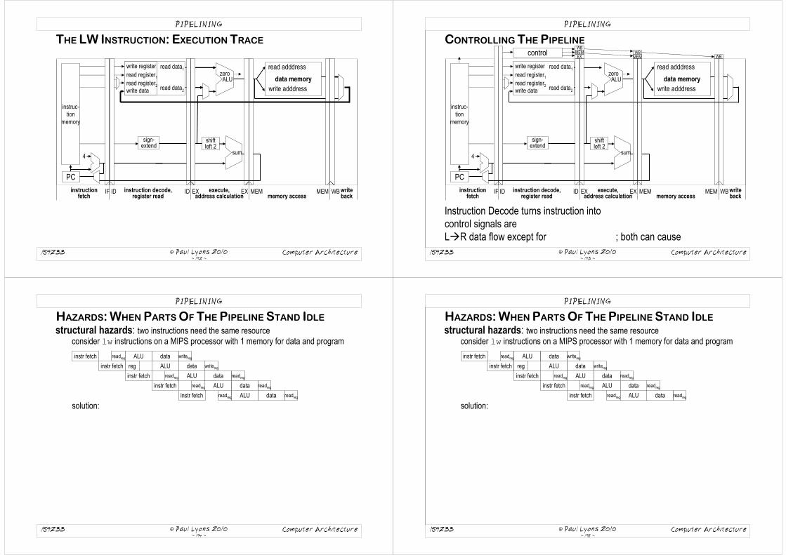
CONTROLLING THE PIPELINE
PIPELINING
Instruction Decode turns instruction intocontrol signals are L�R data flow except for ; both can cause
write register
read register1read register2write data read data2
read data1
ALUzero
data memory
read adddress
write adddress
instruc-tion
memory
PC
4
sign-extend
shiftleft 2
sum
instructionfetch
execute,address calculation memory access
writeback
IF ID EX MEMID EX MEM WBinstruction decode,register read
controlWB
EXWB
WBMEM
MEM
© Paul Lyons 2010~ 194 ~
159233 Computer Architecture
HAZARDS:WHEN PARTS OF THE PIPELINE STAND IDLE
PIPELINING
structural hazards: two instructions need the same resourceconsider lw instructions on a MIPS processor with 1 memory for data and program
instr fetch readreg ALU data writereg
instr fetch reg ALU data writereg
instr fetch readreg ALU data readreg
instr fetch readreg ALU data readreg
instr fetch readreg ALU data readreg
solution:
© Paul Lyons 2010~ 195 ~
159233 Computer Architecture
HAZARDS:WHEN PARTS OF THE PIPELINE STAND IDLE
PIPELINING
structural hazards: two instructions need the same resourceconsider lw instructions on a MIPS processor with 1 memory for data and program
solution:
instr fetch readreg ALU data writereg
instr fetch reg ALU data writereg
instr fetch readreg ALU data readreg
instr fetch readreg ALU data readreg
instr fetch readreg ALU data readreg

© Paul Lyons 2010~ 196 ~
159233 Computer Architecture
HAZARDS:WHEN PARTS OF THEPIPELINE STAND IDLE
PIPELINING
structural hazards: two instructions need the same resourceconsider lw instructions on a MIPS processor with 1 memory for data and program
solution: datapath for pipelined MIPS uses separate instruction and data memories
data hazards: instruction2 needs data before instruction1 has finished producing itadd $s0 $t0 $t1
sub $t2 $s0 $t3
instr fetch readreg ALU data writereg
instr fetch reg ALU data writereg
© Paul Lyons 2010~ 197 ~
159233 Computer Architecture
HAZARDS:WHEN PARTS OF THE PIPELINE STAND IDLE
PIPELINING
structural hazards: two instructions need the same resourceconsider lw instructions on a MIPS processor with 1 memory for data and program
data hazards: instruction2 needs data before instruction1 has finished producing itadd $s0 $t0 $t1
sub $t2 $s0 $t3
instr fetch readreg ALU data writereg
instr fetch reg ALU data writereg
solution1:don't wait for it to bedoesn't work if
solution: datapath for pipelined MIPS uses separate instruction and data memories
© Paul Lyons 2010~ 198 ~
159233 Computer Architecture
HAZARDS:WHEN PARTS OF THE PIPELINE STAND IDLE
PIPELINING
structural hazards: two instructions need the same resourceconsider lw instructions on a MIPS processor with 1 memory for data and program
data hazards: instruction2 needs data before instruction1 has finished producing itadd $s0 $t0 $t1
sub $t2 $s0 $t3
instr fetch readreg ALU data writereg
instr fetch reg ALU data writereg
solution2: controller inserts into the datapath
reg ALU data writereg
solution: datapath for pipelined MIPS uses separate instruction and data memories
control hazards: control decision depends onif (pipelined) instructioni starts on clock cyclen, instructioni+1 starts on cyclen+1
unless instructioni is ; destinationinstr fetch readreg ALU data writereg
instr fetch reg ALU data writereg
solution1:don't wait for it to bedoesn't work if
© Paul Lyons 2010~ 199 ~
159233 Computer Architecture
data hazards: instruction2 needs data before instruction1 has finished producing itadd $s0 $t0 $t1
sub $t2 $s0 $t3 reg ALU data
structural hazards: two instructions need the same resourceconsider lw instructions on a MIPS processor with 1 memory for data and program
instr fetch readreg ALU data writereg
instr fetch
solution2: controller inserts stalls (aka "bubbles") into the datapath
solution: datapath for pipelined MIPS uses separate instruction and data memories
solution1: forward data to next instruction as soon as it's produced don't wait for it to be written to the register filedoesn't work if data is needed before it is produced
control hazards: control decision depends on result of an incomplete instructionif (pipelined) instructioni starts on clock cyclen, instructioni+1 starts on cyclen+1
unless instructioni is a branch instruction; destination not known for 4 more clock cyclesinstr fetch readreg ALU data writereg
instr fetch reg ALU data writereg
HAZARDS:WHEN PARTS OF THE PIPELINE STAND IDLE
PIPELINING
control hazards: control decision depends on result of an incomplete instructionif (pipelined) instructioni starts on clock cyclen, instructioni+1 starts on cyclen+1
unless instructioni is a branch instruction; destination not known for 4 more clock cycles

© Paul Lyons 2010~ 201 ~
159233 Computer Architecture
HAZARDS:WHEN PARTS OF THE PIPELINE STAND IDLE
PIPELINING
control hazards: control decision depends on result of an incomplete instructionif (pipelined) instructioni starts on clock cyclen, instructioni+1 starts on cyclen+1
unless instructioni is a branch instruction; destination not known for 4 more clock cycles
can justput in extra
tests , calculates n &
still have 1 clock-cycle stallor take one alternative anyway
assumeload next instructionstill lose a clock cycle if , but net improvement
improvements:assumeor compiler to use the stall time (MIPS)or on the basis of record
© Paul Lyons 2010~ 202 ~
159233 Computer Architecture
if $s2=0 then
SCHEDULING THE BRANCH DELAY SLOT
PIPELINING
from before from target from fall through
add $s1, $s2, $s3if $s2=0 then
delay slot
add $s1, $s2, $s3
sub $14,$15,$16..add $s1, $s2, $s3if $s1=0 then
delay slot
.
.add $s1, $s2, $s3if $s1=0 then
sub $14,$15,$16
add $s1, $s2, $s3if $s1=0 then
sub $14,$15,$16
delay slot
add $s1, $s2, $s3if $s1=0 then
sub $14,$15,$16
© Paul Lyons 2010~ 203 ~
159233 Computer Architecture
BRANCH PREDICTION
PIPELINING
small memory indexed byeach location has 1 bit - set a bit , resetwill sometimes be setprediction unrelated tobut will contain
but consider performance of a loop branchtaken times, not taken once mispredictionbut after last iteration, prediction isso misprediction atbranch taken 90% of time, correct prediction 80% of time
use 2-bit branch prediction memorymust be wrong twice before prediction changescopes with repeated loops
predict taken predict taken
not taken
taken
not taken
predict taken
taken
taken
taken
predict taken
not taken
not taken
© Paul Lyons 2010~ 204 ~
159233 Computer Architecture
DATA HAZARDS - CATEGORISATION
PIPELINING
RAW – Read After Write
WAR – Write After Read
WAW – Write After Write
in each of the hazards below, instructioni starts executing before instructionjhazard name refers to what should happen, not what goes wrong (!)

© Paul Lyons 2010~ 205 ~
159233 Computer Architecture
RAWHAZARDS
EXCEPTIONS
four situations – 2 problematic, 2 not
LW R1,45,(R2)DADD R5,R6,R7DSUB R8,R6,R7OR R9,R6,R7
LW R1,45(R2)DADD R5,R1,R7DSUB R8,R6,R7OR R9,R6,R7
LW R1,45,(R2)DADD R5,R6,R7DSUB R8,R1,R7OR R9,R6,R7
LW R1,45(R2)DADD R5,R6,R7DSUB R8,R6,R7OR R9,R1,R7
nothing in following 3 instructions depends on R1(4th following instruction will be in IF when 1st is in WB)
hardware detects phase1 R1 write, phase2 R1 readstalls DADD instruction's EX phase(& following instructions)
hardware detectsforwards
no action required. Write of R1 occurs during 1st half of DSUB's ID phase, and read occurs in 2nd half
© Paul Lyons 2010~ 206 ~
159233 Computer Architecture
WHEN TO FORWARD IN EXPHASE
EXCEPTIONS
sourceinstruction
destinationinstruction forward if:
R-type R-typeI-type, lw, sw, bra
destinationtop ALU i/p
EX/MEM[rd] = ID/EX[rs]
R-type R-type
R-type R-typeI-type, lw, sw, bra
R-type R-type
I-type
R-typeI-type, lw, sw, bra
lw
EX/MEM[rd] = ID/EX[rt]
MEM/WB[rd] = ID/EX[rs]
MEM/WB[rd] = ID/EX[rt]
bottom ALU i/p
top ALU i/p
bottom ALU i/p
top ALU i/p
bottom ALU i/p
top ALU i/p
bottom ALU i/p
top ALU i/p
bottom ALU i/p
R-typeI-type, lw, sw, bra EX/MEM[rt] = ID/EX[rs]
I-type R-type EX/MEM[rt] = ID/EX[rt]
I-type
I-type
lw
R-typeI-type, lw, sw, bra
R-type
R-type
MEM/WB[rt] = ID/EX[rs]
MEM/WB[rt] = ID/EX[rt]
MEM/WB[rt] = ID/EX[rs]
MEM/WB[rt] = ID/EX[rt]
EX/MEM[rd] = ID/EX[rs]
© Paul Lyons 2010~ 207 ~
159233 Computer Architecture
THE IDEAL, THE REALITY
MEMORY MANAGEMENT
The ideal indefinite memory capacityrandom accessany word instantly available
The reality limited memory capacityfinite speedshigh speeds � high costshigh capacity � low speed
The solutionhierarchy of memories, with processor registers at the topeach step down has more capacity but slower access
, & THE SOLUTION
© Paul Lyons 2010~ 210 ~
159233 Computer Architecture
MEMORY MANAGEMENT
THE SOLUTION
archiveprocessorregisters
main(I0)
memory
backing(20)store
VirtualMemory
auto archivaland
file retrieval
Memory management blurs the distinctions to make memory seem as possibleas possibleas possibleas possible

© Paul Lyons 2010~ 211 ~
159233 Computer Architecture
ALTERNATIVE VIEW
MEMORY MANAGEMENT
CPU
levels in the memory hierarchy
level 1
level 2
level n
increasing distance from the CPU in access time
size of the memory at each level
© Paul Lyons 2010~ 212 ~
159233 Computer Architecture
PRINCIPLE(S) OF LOCALITY
MEMORY MANAGEMENT
is liable to beprinciple of
only a small proportion is of interest at any time
is liable to be followedprinciple of
on memory reference:bring item fromto SRAM: fast, but expensive and thus smallfrom which
in code, is liable to be followed byprinciple of (special case of preceding principle)
(and ask it )
© Paul Lyons 2010~ 213 ~
159233 Computer Architecture
AIMS
MEMORY MANAGEMENT
aims: to make memory behaveas asas as
technique:on a hit,on a miss,may need to transfer from to
hit ratio:miss ratio:miss penalty:hit time:
© Paul Lyons 2010~ 214 ~
159233 Computer Architecture
CACHE
MEMORY MANAGEMENT - cache
small, fast between registers and
how do we map the large DRAM address space onto the small SRAM?
direct-mapped cacheaddress in cache with 2n locations is just
0000000100100011010001010110011110001001101010111100110111101111
M
000001010011100101110111
cache

© Paul Lyons 2010~ 215 ~
159233 Computer Architecture
ACCESSING AWORD IN CACHE – the Write Back strategy
MEMORY MANAGEMENT - cache
32 bit addressfrom processor
data
32
tag address
22Cache
1024
decoder
10-bit cache register address
23-bit tag address
tristate buffers
match1
55
23-bit residualfrom cache
data part32
changed bit1
residualsequal?
R 1 0 take data from cacheTag valueMatchR/W Tag action Cache / memory action
R 1 1 take data from cacheR 0 0 read memory to cacheR 0 1 clear write old data to memory, read new word from memoryW 1 0 set write data to cache W 1 1 write data to cacheW 0 0 set write new data & address to cacheW 0 1 set write old data to memory, new data & address to cache
changedbit
1
© Paul Lyons 2010~ 216 ~
159233 Computer Architecture
ACCESSING AWORD IN CACHE
MEMORY MANAGEMENT - cache
R 1 0 take data from cacheTag valueMatchR/W Tag action Cache / memory action
R 1 1 take data from cacheR 0 0 read memory to cacheR 0 1 clear write old data to memory, read new word from memoryW 1 0 set write data to cache W 1 1 write data to cacheW 0 0 set write new data & address to cacheW 0 1 set write old data to memory, new data & address to cache
32 bit addressfrom processor
data
32
tag address
22Cache
1024
decoder
10-bit cache register address
23-bit tag address
tristate buffers
match1
55
23-bit residualfrom cache
data part32
changed bit1
residualsequal?
changedbit
1
© Paul Lyons 2010~ 217 ~
159233 Computer Architecture
OTHER FLAVOURS OF CACHE
MEMORY MANAGEMENT - cache
(Guava, Loganberry, Snail)
changed bit is not always usedwhen a cache location is overwrittenits impossible to tellalways write cache data back to memory whenSimple Swap strategy
OR Write-Through (even simpler)always write data to cache & back to memory whennot as inefficient as you might think;buffer queue stores data & address so
processor cache
Memory
buffer queue
© Paul Lyons 2010~ 218 ~
159233 Computer Architecture
ASSESSING CACHE UPDATE ALGORITHMS
MEMORY MANAGEMENT - cache
cycle time
write-through
simple swap
0.7 0.8 0.9 1.0
HR
flagged swapbuffered swap

© Paul Lyons 2010~ 219 ~
159233 Computer Architecture
BLOCK TRANSERS
MEMORY MANAGEMENT - cache
temporal locality supported by
spatial locality requires
© Paul Lyons 2010~ 220 ~
159233 Computer Architecture
BLOCK SIZE INFLUENCES MISS RATE
MEMORY MANAGEMENT - cache
1 KB
16 KB
256 KB64 KB
256
40%
35%
30%
25%
20%
15%
10%
5%
0%
Miss rate
64164
Block size (bytes)
8 KB
block in memory
first word referenced
© Paul Lyons 2010~ 221 ~
159233 Computer Architecture
HANDLING ACACHE MISS
MEMORY MANAGEMENT - cache
what happens to the current instruction when a cache miss occurs?
consider a miss when loading an instruction instruction register containswe'll have to when the value has loadedPC � (because )initiatewrite ; reset
© Paul Lyons 2010~ 222 ~
159233 Computer Architecture
INTRINSITY FASTMATH PROCESSOR CACHES
MEMORY MANAGEMENT - cache
cache index
=tag
data
data512tag
18
V1 32
012
56
13
14
31
256
block offset
hit
instruction miss rate:data miss rate:

© Paul Lyons 2010~ 223 ~
159233 Computer Architecture
TRANSFERRING BLOCKS EFFICIENTLY
MEMORY MANAGEMENT - cache
memory speed puts on latency of access to 1st word of a block
wider memory & bus allowno reductionoverall transfer rate
memory bus clock cycles
to send addressto access datato send data
1 word
4 words
(10 longer than processor cycles)
bus and memory width
cache block width
1 x 115 x 44 x 1
65miss penalty
bandwidth achieved4 x 465
= 0.25 words/cycle
© Paul Lyons 2010~ 224 ~
159233 Computer Architecture
TRANSFERRING BLOCKS EFFICIENTLY
MEMORY MANAGEMENT - cache
memory speed puts lower limit on latency of access to 1st word of a block
wider memory & bus allow parallel transfer of complete blockno reduction I latency of 1st wordoverall transfer rate higher
bus and memory width
cache block width
memory bus clock cycles
to send addressto access datato send data
1 word
4 words
1 x 115 x 44 x 1(10 longer than processor cycles)
2 words
4 words 4 words
4 words
1 x 115 x 2
1 x 115 x 1
65
2 x 1
33
1 x 1
17miss penalty
bandwidth achieved4 x 465
4 x 433
4 x 417
= 0.48 words/cycle
= 0.94words/cycle
- Wider Memory And Bus
= 0.25 words/cycle
© Paul Lyons 2010~ 225 ~
159233 Computer Architecture
TRANSFERRING BLOCKS EFFICIENTLY
MEMORY MANAGEMENT - cache
- Interleaved Memory
M
cache
CPU
M
cache
CPU
M1 M2 M3 M4
cache
CPU
1-word widememory
multi-word widememory
interleavedmemories
all memories can read in
parallel
single-word buscycle count: 1 to send address15 to access memory4 x 1 to send databandwidth
= (4 x 4) /20= 0.8 words/cycle
© Paul Lyons 2010~ 226 ~
159233 Computer Architecture
CACHE DESIGN ISSUES
MEMORY MANAGEMENT - cache
placement policy
size of blocks transferred to and stored in cache
memory update policy
cache size
replacement policy

© Paul Lyons 2010~ 227 ~
159233 Computer Architecture
MEASURING AND IMPROVING CACHE PERFORMANCE
MEMORY MANAGEMENT - cache
memory stall cycles
=
total CPU time = cycle time x (useful execution cycles + stall cycles)
© Paul Lyons 2010~ 228 ~
159233 Computer Architecture
MEASURING AND IMPROVING CACHE PERFORMANCE
MEMORY MANAGEMENT - cache
consider a machine with separate instruction and data cachesproccessor CPI (without memory stalls): 2miss penalty(all misses) 100 cycles for a particular program:
instructions executed I
loads and stores as % of total instructions 36%data cache miss rate 4%instruction cache miss rate 2%
how much faster would the program be if we eliminated misses?
total miss cycles = +
© Paul Lyons 2010~ 229 ~
159233 Computer Architecture
MEASURING AND IMPROVING CACHE PERFORMANCE
MEMORY MANAGEMENT - cache
consider a machine with separate instruction and data cachesproccessor CPI (without memory stalls): 2miss penalty(all misses) 100 cycles for a particular program:
instructions executed I
loads and stores as % of total instructions 36%data cache miss rate 4%instruction cache miss rate 2%
how much faster would the program be if we eliminated misses?
total miss cycles = +
CPI including memory stalls = + =now, speed is IPC = 1/CPIspeed increase =
© Paul Lyons 2010~ 231 ~
159233 Computer Architecture
MEASURING AND IMPROVING CACHE PERFORMANCE
MEMORY MANAGEMENT - cache
how much faster would the program be if we eliminated misses?speed increase = 2.72
what about improving the processor performance?let's try reducing the Cycles Per Instruction by 50%
CPIno misses memory stalls CPItotal2 3.44 5.441 3.44 4.44
existing processor: improved processor:
remember Amdahl's Law?max speedup = total time/time that can be reduced to 0
speed increase = 1.18

© Paul Lyons 2010~ 232 ~
159233 Computer Architecture
MEASURING AND IMPROVING CACHE PERFORMANCE
MEMORY MANAGEMENT - cache
how much faster would the program be if we eliminated misses?speed increase = 2.72
what about improving the processor performance?let's try reducing the Cycles Per Instruction by 50%
speed increase = 1.18let's try doubling the clock rate (memory read/write times don’t change)
miss penalty = 200 clock cycles (previously 100)total miss cycles = instruction misses + data misses
= I x 0.02 x 200 + I x 0.36 x 0.04 x 200 = 6.88 I
CPI = 2 + 6.88 = 8.88
speed increaseexecution timefastclock
execution timeslow clock= =
I x CPI1 x clock cycle1
I x CPI2 x 0.5 x clock cycle1
= 5.44 / (8.88 x 0.5)= 1.23
© Paul Lyons 2010~ 234 ~
159233 Computer Architecture
MEASURING AND IMPROVING CACHE PERFORMANCE
MEMORY MANAGEMENT - cache
how much faster would the program be if we eliminated misses?speed increase = 2.72
what about improving the processor performance?let's try reducing the Cycles Per Instruction by 50%
speed increase = 1.18let's try doubling the clock rate (memory read/write times don’t change)
speed increase = 1.23
cache misses (& Amdahl) reduce impact of other improvementsincreasing clock rate AND decreasing CPI incurs a double hit
with reduced cycles per instruction stall cycles/overall cycles increaseswhen processor clock speeds increase, memory clock speeds don'tmiss penalty high clock speed processor > miss penalty low clock speed processor
good cache design helps performance as much as increasing processor speed
© Paul Lyons 2010~ 235 ~
159233 Computer Architecture
ALTERNATIVE PLACEMENT POLICIES
MEMORY MANAGEMENT - cache
there are various schemes for placing blocks in cacheintended to reduce cache misses
direct mappingcache index bits are subset of memory address,each block of memory locations has only one possible cache destination
fully associative mappingmemory blocks go anywhere in cache, source address is stored with themcache access involves comparing address tag & cache tag at every cache location multiple comparators � expensive hardwaresuitable for L1 (only a few words) caches only
set-associative mappingn-way SA cache has n blockseach memory block maps to any element of a unique subset ( >=2) of the cache blocksmapping to set is direct, mapping within set is associative
© Paul Lyons 2010~ 236 ~
159233 Computer Architecture
INDICATIVE DIAGRAMS
MEMORY MANAGEMENT - cache
direct mapping
set associativemappings
fully associative mapping

© Paul Lyons 2010~ 237 ~
159233 Computer Architecture
FORMAL SPECIFICATIONS
MEMORY MANAGEMENT - cache
Consider a system with memory and cache both organised into blocksblocksize, b = 2w words, for some wlines in cache, L = 2k1 => cachesize = 2k1+w wordsblocks in memory, B = 2k2 => memorysize = 2k2+w wordshence addresses are k2 + w bits long
IfL = 4, k1 = 2B = 8, k2 = 3b = 4, w = 2
then these mappings hold:M0 � C0
M4 � C0
M1 � C1
M5 � C1
etc.
- DIRECT MAPPING
block line j = i mod L (i is memory block)
7
6
5
4
3
2
1
0
Block frame
3
2
1
0
Block no
M
C
wk 2 real address
k 1 wtag cache address
© Paul Lyons 2010~ 238 ~
159233 Computer Architecture
FORMAL SPECIFICATIONS
MEMORY MANAGEMENT - cache
direct mapping desired data may be in only one cache locationthough mapping is many-to-one
fully associative mapping desired data may be in several cache locationsthe one which contains the word addressed (if any) must then be identifiedmany-to-many mapping
again, divide memory into 2k2 blocks of 2w words. (k2 + w)-bit addresses each cache line contains data field (2w words)a tag field (top k2 bits of the block's address)equality-detect circuit (tag field = top k2 bits of address)
at each memory referenceif tag matches, cache contains the addressed datathe equality detect signal acts as a "line select" to allow I/O on the appropriate word of the line
- Fully Associative Mapping
© Paul Lyons 2010~ 239 ~
159233 Computer Architecture
4-WAY FULLY-ASSOCIATIVE CACHE
MEMORY MANAGEMENT - cache
cacheindex
012
9
10
31
dataV
tag
dataV
tag tag
dataV
tag
dataV
tag
hit
data
© Paul Lyons 2010~ 240 ~
159233 Computer Architecture
SET-ASSOCIATIVE CACHE
MEMORY MANAGEMENT - Cache
amalgam of direct and associative schemescache has structurelines are grouped intoblock has words - as beforememory organisationcache has
wk 2 real address
block index
stored in cache with data
wtag cache addressk 0
set no
mapping works at firstset j = i mod S (i is a block in main memory)
Then, after :associative search for blockThen: to find specific word

© Paul Lyons 2010~ 241 ~
159233 Computer Architecture
012
91011
tag
dataV
tag
dataV
tag
dataV
tag
dataV
2-WAY SET-ASSOCIATIVE CACHE
MEMORY MANAGEMENT - cache
31
cacheindex
= =
set
==
hit
data
© Paul Lyons 2010~ 242 ~
159233 Computer Architecture
L1, L2, L3
MEMORY MANAGEMENT - Cache
L1 cachetypically 8KB - 128KBpart of processor corefast technology (SRAM)processor speed
L2 cachetypically 256KB - 1MBoriginally off chip; now often on½ or ¼ processor speed
L3 cacheincreasingly commontypically 16MB - 256MBoff chip (but sometimes on the same die)expensive; used in high-end processors½ L2 cache speed
Some L2 and even L3 caches run at processor speeds.
So what's the point of smaller L1 cache?
A more sophisticated, more expensive, more efficient memory mapping policy is desirable but only cost-effective on a small scale???
© Paul Lyons 2010~ 243 ~
159233 Computer Architecture
MEMORY MANAGEMENT - Cache
128 KB L1 + 256 KB L2AMD Athlon Thunderbird
128 KB L1 + 64 KB L2AMD Duron
128 KB L1AMD K7 Athlon
64 KB L1 + 256 KB L2AMD K6-3
32 KB L1 + 256 KB L2Pentium III Cumine
32 KB L1 + 128 KB L2Celeron
32 KB L1Pentium II and III
64 KB L1AMD K6 and K6-2
32 KB L1Pentium MMX
16 KB L1 + 256 KB L2
(some 512 KB L2)
Pentium Pro
16 KB L1Pentium
16 KB L180486DX4
8 KB L180486DX and DX2
Cache size in the CPUCPU
© Paul Lyons 2010~ 244 ~
159233 Computer Architecture
registersL1 cache(16KB)
Pentium CPU
MEMORY MANAGEMENT - Cache
L2 cache(256KB)
RAM(32M)
system bus
more modern processors: L2 cache on the processor chip
CPUL2 cache
I/O busses

© Paul Lyons 2010~ 245 ~
159233 Computer Architecture
BLOCK REPLACEMENT POLICY
MEMORY MANAGEMENT - Cache
direct mapping cacheno choice; incoming block can only go into one slot
associative cacheany block could go
set-associative cacheincoming block can only go into one setany block in selected set could go
FIFO
Least Recently Used; significantly better performance than FIFO
each set has a reference numberwhen set with reference no. n is referenced
reference nos < n are incrementedreference no of referenced set is set to 0
block-to-go is always block with largest reference numberexpensive hardware when sets are large.
© Paul Lyons 2010~ 246 ~
159233 Computer Architecture
THE NEXT PHASE
MEMORY MANAGEMENT – virtual memory
archiveprocessorregisters
main(I0)
memory
backing(20)store
câcheL1, L2, L3
VirtualMemory
auto archivaland
file retrieval
Memory management blurs the distinctions to make memory seem as big as possibleas fast as possibleas cheap as possibleas secure as possible
VirtualMemory
© Paul Lyons 2010~ 247 ~
159233 Computer Architecture
VIRTUAL MEMORY'S RAISONS D'ETRE
MEMORY MANAGEMENT – virtual memory
Original VM let programs use a memory space larger than physical memoryprogrammers had to divide programs into mutually exclusive overlays (code & data)program had to control loading of its own overlaysVM automatically maps program pages onto physical memory addresses
Also allowed multiple programs to run simultaneously independent virtual address spaces memory protectionpredominant use today
installed memory
program 1
program 2
program 3
program 4
individually smaller, together larger
© Paul Lyons 2010~ 248 ~
159233 Computer Architecture
GENERAL IDEA
MEMORY MANAGEMENT – virtual memory
program code and data are stored as fixed-sized units called pagespages live on disk, have a disk address, are copied into memory when necessarymemory operations use (Virtual Page no, page offset)
program's code (and data) pages don’t have to be contiguous
address translation unit converts VP no. into base address of page in physical memorybase address + page offset produces real address of databits in offset� page size
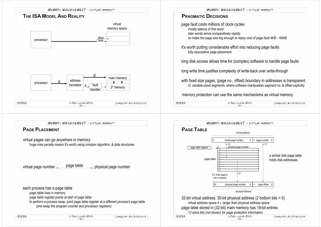
© Paul Lyons 2010~ 250 ~
159233 Computer Architecture
THE ISAMODEL AND REALITY
MEMORY MANAGEMENT – virtual memory
offsetprocessor
virtual memory space
base
faulthandler
20 memoryo
processoraddresstranslator
main memorya
a'
© Paul Lyons 2010~ 251 ~
159233 Computer Architecture
PRAGMATIC DECISIONS
MEMORY MANAGEMENT – virtual memory
page fault costs millions of clock cyclesmostly latency of first wordlater words arrive comparatively rapidlyso make the page size big enough to repay cost of page fault 4KB – 64KB
it's worth putting considerable effort into reducing page faultsfully associative page placement
long disk access allows time for (complex) software to handle page faults
long write time justifies complexity of write-back over write-through
with fixed size pages, (page no., offset) boundary in addresses is transparentcf. variable-sized segments, where software manipulates segment no. & offset explicitly
memory protection can use the same mechanisms as virtual memory
© Paul Lyons 2010~ 252 ~
159233 Computer Architecture
PAGE PLACEMENT
MEMORY MANAGEMENT – virtual memory
virtual pages can go anywhere in memoryhuge miss penalty means it's worth using complex algorithm, & data structures
virtual page number physical page number page table
each process has a page tablepage table lives in memorypage table register points at start of page tableto perform a process swap, point page table register at a different process's page table
(and swap the program counter and processor registers)
© Paul Lyons 2010~ 253 ~
159233 Computer Architecture
V physical page number
PAGE TABLE
MEMORY MANAGEMENT – virtual memory
page table register
page table
if 0, then page is not in memory
011 page offset
12
physical address
0
virtual address
111231 virtual page number page number
32-bit virtual address, 30-bit physical address (2 bottom bits = 0)virtual address space 4 x larger than physical address space
page table stored in (32-bit) main memory has 19-bit entries13 extra bits (not shown) for page protection information
1229 physical page number
18
20
a similar disk page table holds disk addresses

© Paul Lyons 2010~ 254 ~
159233 Computer Architecture
PAGE FAULTS
MEMORY MANAGEMENT – virtual memory
not all of a program's pages have to be in memory while it's runningonly pages that have been referenced since the process was swapped in
but disk space is much more abundantOS usually reserves enough disk space for all the process's pagescalled the swap space
OS is responsible for handling page faultshardware detects that valid bit for selected page is FALSE
© Paul Lyons 2010~ 255 ~
159233 Computer Architecture
PAGE REPLACEMENT
MEMORY MANAGEMENT – virtual memory
if the OS needs to bring in a page and all pages in the swap space are in useit must oust a pagewhich page? swap space is a fully associative store
?
page-to-go should be about to be unused for as long as possible predicting the future is a difficult businessprediction: Least Recently Used page will be Furthest Future Use page
ousted page goes to swap space
strict LRU algorithm would collect stats at every memory referencetoo expensiveinstead, each page references sets a reference bit for the pagereset periodically, tested after standard delayany page with reference bit still reset is Not Recently Used – can be paged out
© Paul Lyons 2010~ 256 ~
159233 Computer Architecture
for a machine with 32-bit addresses, 32-bit page table entries and 4KB pages how many page table entries? 232 / 212 = 220
how big is the page table? 220 x 22 = 222 B = 4MBso, maybe 400MB in total
PAGE TABLE SIZES
MEMORY MANAGEMENT – virtual memory
typically scores or hundreds of processes running at a time
how to minimise memory usage generally and size of page table in particular?use dynamically-sized page table; only big if program is page-greedy
keep last page register (aka page limit register)forces page table to grow in 1 direction only
but stack and heap usually grow in opposite directions
code
processes' address space
static data (constants, arrays)dynamic data (lists, trees)
stack
© Paul Lyons 2010~ 257 ~
159233 Computer Architecture
PAGE TABLE SIZES
MEMORY MANAGEMENT – virtual memory
for a machine with 32-bit addresses, 32-bit page table entries and 4KB pages how many page table entries? 232 / 212 = 220
how big is the page table? 220 x 22 = 222 B = 4MBso, maybe 400MB in total
typically scores or hundreds of processes running at a time

© Paul Lyons 2010~ 258 ~
159233 Computer Architecture
PAGE TABLE SIZES
MEMORY MANAGEMENT – virtual memory
how to minimise memory usage generally and size of page table in particular?use dynamically-sized page table; only big if program is page-greedy
keep last page register (aka page limit register)forces page table to grow in 1 direction only
but stack and heap usually grow in opposite directionsseparate page tables, with 2 page limit registers, 1 for up, 1 for downtop bit of address differentiates between top & bottom segments of address space
inverted page table only in-use pages are stored; can't use address to index page's entry, must searchto reduce search time, hash the addresses' entries
multi-level (tree-structured) page table complex, but suits non-contiguous pageshighest order bits address a "segment"; if valid, lower bits address page in segment
page the page tableincreases no. of page faults; lock some pages of page table in memory
© Paul Lyons 2010~ 259 ~
159233 Computer Architecture
HANDLING WRITE OPERATIONS
MEMORY MANAGEMENT – virtual memory
cache can use writethroughmemory only hundreds of times slower than registers small writethrough buffer masks write latency
VM write has to wait for disk accessmillions of clock cyclesbuffer would be impracticalwriteback used insteaddisk write only occurs when essential – when OS overwrites a dirty page in memory
© Paul Lyons 2010~ 260 ~
159233 Computer Architecture
THE TLB – HANDLING THE OVERHEAD
MEMORY MANAGEMENT – virtual memory
page table resides in memoryordinary read or write (Instr. Fetch or lw/sw instruction) involves 2 memory accesses
1 to convert virtual address to physical address
1 to access the data
to reduce memory referencesprinciple of locality applies to page table entries tooTranslation Lookaside Buffer is a translation cache
cf. scraps of paper provided by libraries for writing library call no. onmaintains list of locations of a subset of pagesreplacement policy difficult
software too slow; hardware too expensive for complex policy (e.g.LRU)often randomly choose entry-to-go
© Paul Lyons 2010~ 262 ~
159233 Computer Architecture
TLBCIRCUIT OUTLINE
MEMORY MANAGEMENT – virtual memory
virtual address
0111231 12-bit page offset20-bit virtual page number
Tag Physical Page Number
=
=
=
=
==
V Dirty
hit
TLB
Physical Page Number Page Offset
20
Physical Address Tag
256cache
byteoffset
4
blockoffset
data
Cache Index
8
16
18
= hit
if no hit in TLB, use page tableif no hit there, get page from diskif no cache hit, use memory

© Paul Lyons 2010~ 263 ~
159233 Computer Architecture
cache
TLBCIRCUIT OUTLINE
MEMORY MANAGEMENT – Virtual Memory
virtual address
0111231 12-bit page offset20-bit virtual page number
Tag Physical Page Number
TLB
Physical Page Number Page Offset
20
Physical Address Tag
cache
byteoffset
4
blockoffset
data
Cache Index
818
= hit
if no hit in TLB, use page tableif no hit there, get page from diskif no cache hit, use memory
data
Cache Index
8
© Paul Lyons 2010~ 264 ~
159233 Computer Architecture
USING THETLBFOR AREAD/WRITE OPERATION
MEMORY MANAGEMENT – virtual memory
virtual address
TLB access
TLB hit?
Yes: TLB provides physical address
No Yeswrite?
No Yeswrite accessbit on?
write protectionexception
write data into cacheupdate the tag
put data & address intothe write buffer
TLB missexception
No
Try to read datafrom cache
cache miss stallNo Yes
cache hit?
deliver data to the CPU
© Paul Lyons 2010~ 265 ~
159233 Computer Architecture
THE SYNERGY BETWEEN VMAND MEMORY PROTECTION
MEMORY MANAGEMENT – virtual memory
Machines run multiple processes "simultaneously"on single processor machines only one process is active at a timesimple multitasking swaps between processes when I/O occurspreemptive multtasking swaps at short intervals
gives users on multiuser systems the impression of sole accessallows modern multiprocessing systems to handle hundreds of processes
activeprocess
processesengaged in I/O
I/Orequest
readyprocesses
I/O terminates
© Paul Lyons 2010~ 267 ~
159233 Computer Architecture
THE SYNERGY BETWEEN VMAND MEMORY PROTECTION
MEMORY MANAGEMENT – virtual memory
Machines run multiple processes "simultaneously"on single processor machinessimple multitaskingpreemptive multtasking
gives usersallows modern multiprocessing systems to
VM allows processesa process's pages can bewhat if one process addresses outside its own space?

© Paul Lyons 2010~ 268 ~
159233 Computer Architecture
PROTECTION REQUIREMENTS
MEMORY MANAGEMENT – virtual memory
separate user and OS (supervisor) modessome instructions available
ability to make certain information read-only for user processes
mechanism for swapping between modestransfers control to
store in return from exception
put page tables inallows OS toprevents user process fromprevents user process from
© Paul Lyons 2010~ 269 ~
159233 Computer Architecture
IMPLEMENTING APROCESS SWITCH
MEMORY MANAGEMENT – virtual memory
on a machine without a TLB, this is comparatively simplepoint page table register at
consider a switch from P1 to P2
on a machine with a TLBneed toneed to
replacing all of P1's entries in TLB can be inefficient if:
problem; virtual address spaces the samesolution: make them different
give each processOS remembers putat each memory access,
© Paul Lyons 2010~ 270 ~
159233 Computer Architecture
SHARING INFORMATION
MEMORY MANAGEMENT – virtual memory
in general, one process should not be able toTLB has that prevents a process from
sometimes processes need to be able to share informationP1 wants to access information in a page owned by P2
process P2 asks OS to create a new page table entry page table entry goes into P1's virtual address space but accesses P2's physical page P2 can ask OS to set write protection bit in P1's page so P1 can't update the page