1502 ieee transactions on electron devices, vol. 63, no....
TRANSCRIPT

1502 IEEE TRANSACTIONS ON ELECTRON DEVICES, VOL. 63, NO. 4, APRIL 2016
Analysis of 7/8-nm Bulk-Si FinFET Technologiesfor 6T-SRAM Scaling
Xi Zhang, Senior Member, IEEE, Daniel Connelly, Member, IEEE, Peng Zheng, Student Member, IEEE,Hideki Takeuchi, Member, IEEE, Marek Hytha, Senior Member, IEEE, Robert J. Mears,
and Tsu-Jae King Liu, Fellow, IEEE
Abstract— The benefits of a super-steep retrograde (SSR) findoping profile, which can be achieved using the oxygen insertiontechnology, are quantified via 3-D technology computer-aideddesign simulations for the 7/8-nm bulk-Si FinFET technologytargeting low-power applications. A calibrated compact modelis then used to estimate the six-transistor static RAM cellperformance and yield. The SSR FinFET technology is projectedto provide for up to 100 mV reduction in minimum cell supplyvoltage, to facilitate voltage scaling to below 0.50 V.
Index Terms— FinFET, six-transistor (6T) staticRAM (SRAM), super-steep retrograde (SSR), variability.
I. INTRODUCTION
F inFETs have been adopted for the high-volume productionof CMOS integrated circuits beginning at the 22-nm
technology generation [1], due to the superior electrostaticintegrity of these multigate transistor structures. Althoughsilicon-on-insulator wafers are ideal substrates for the man-ufacture of FinFETs with low OFF-state leakage current [2],they are much more expensive than the conventional bulk-si wafers. If a bulk-si wafer is used as the substrate forFinFET fabrication, then heavy punch-through stopper (PTS)doping is needed at the base of the fins to suppress OFF-stateleakage current. A conventional doping process results indopants within the fin (channel region), on the order of5 × 1017 cm−3, which degrades transistor ON-state current.In addition, heavy channel doping results in increased process-induced variations in transistor performance, which pose aserious challenge for achieving sufficiently high yield for largestatic RAM (SRAM) arrays. In this paper, the benefits of a
Manuscript received November 9, 2015; revised January 26, 2016; acceptedJanuary 28, 2016. Date of current version March 22, 2016. The work ofX. Zhang was supported by the Maxine Pao Memorial Scholarship Fund. Thereview of this paper was arranged by Editor R. M. Todi.
X. Zhang, D. Connelly, and P. Zheng are with the Department of ElectricalEngineering and Computer Sciences, University of California at Berkeley,Berkeley, CA 94720 USA (e-mail: [email protected]; [email protected]; [email protected]).
H. Takeuchi, M. Hytha, and R. J. Mears are with Mears Technologies, Inc.,Newton, MA 02459 USA (e-mail: [email protected];[email protected]; [email protected]).
T.-J. K. Liu is with the Department of Electrical Engineering and ComputerSciences, University of California at Berkeley, Berkeley, CA 94720 USA, andalso with the Kavli Energy NanoScience Institute, Berkeley, CA 94720 USA(e-mail: [email protected]).
Color versions of one or more of the figures in this paper are availableonline at http://ieeexplore.ieee.org.
Digital Object Identifier 10.1109/TED.2016.2523885
Fig. 1. Simulated 3-D n-channel FinFET structures. The net dopantconcentration is represented in color using a hyperbolic arcsine scale.
super-steep retrograde (SSR) fin doping profile, which can beachieved using the oxygen insertion technology [3], are quanti-fied via 3-D device technology computer-aided design (TCAD)simulations for the 7/8-nm bulk-si FinFET technology target-ing low-power applications. The benefits of the SSR FinFETtechnology [4] for facilitating reductions in six-transistor (6T)static memory (SRAM) cell operating voltage are quantified.
II. BULK-Si FinFET DESIGN OPTIMIZATION
Fig. 1 shows a perspective view of the 3-D FinFETstructures simulated using Sentaurus Device [5] in this paper.The gate length (Lgate) is 15 nm, which corresponds to the7/8-nm technology node in the International TechnologyRoadmap for Semiconductors (ITRS) [6]. The equivalent gate-oxide thickness is 0.64 nm. The fin height (HSi) is 40 nm,the fin width (WSi) is 8 nm, so that the fin aspect ratiois 5, and the fin pitch is 30 nm based on Intel 22-nm [1]and 14-nm FinFET technology [7]. The gate work function isassumed to be tunable to achieve an OFF-state leakage currentspecification (IOFF) of 30 pA/μm (consistent with TSMC’s16-nm FinFET technology [8]) for low-power applications.The current is normalized to the effective channel width (Weff),which is defined as the peripheral length of the silicon finregion. The fin shape is rectangular with rounded corners(1-nm radius of curvature) for reduced gate leakage andenhanced gate control [9], as in the Intel’s 14-nm FinFETtechnology [7]. The thickness of the shallow trench isolationoxide is 50 nm. The FinFET structures each comprise heavily
0018-9383 © 2016 IEEE. Personal use is permitted, but republication/redistribution requires IEEE permission.See http://www.ieee.org/publications_standards/publications/rights/index.html for more information.
ZHANG et al.: ANALYSIS OF 7/8-nm BULK-Si FinFET TECHNOLOGIES 1503
TABLE I
BULK-Si FinFET DESIGNS: NOMINAL PARAMETER VALUES
doped raised source/drain (S/D) regions formed by selectiveepitaxial growth (SEG) [10], for reduced parasitic resistance.In this paper, the S/D junctions are assumed to have aGaussian doping profile with 2-nm/decade gradient and peakconcentrations 2 × 1020 cm−3 [11]. The SEG S/D regionscomprise doped silicon for n-channel FinFETs (nFETs), andsilicon-germanium (SiGe) with 50% germanium concentra-tion [1] for p-channel FinFETs (pFETs), with parameter valuestaken from [12]. Ohmic contacts (specific contact resistivity3 × 10−9 � · cm2) are made only to the top surfaces of theSEG S/D regions. Table I summarizes the nominal values ofthe various design parameters for the control FinFETs and theSSR FinFETs.
The TCAD software package Sentaurus Device [5] was usedto simulate the FinFET performance using the drift-diffusiontransport model [13] calibrated to the ballistic Monte Carlosimulations, the Philips unified model for carrier mobility,the bandgap narrowing model, the density gradient quanti-zation model, and the nonlocal-path trap-assisted tunnelingmodel [14]. The fin sidewall surfaces (along which the tran-sistor current flows) are assumed to be {110} crystallographicplanes, with transistor current flow in a 〈110〉 direction.To boost transistor ON-state current, 2-GPa (tensile) uniax-ial stress is induced in the fin channel region for nFETs,whereas −2-GPa (compressive) uniaxial stress is induced inthe fin channel region for pFETs.
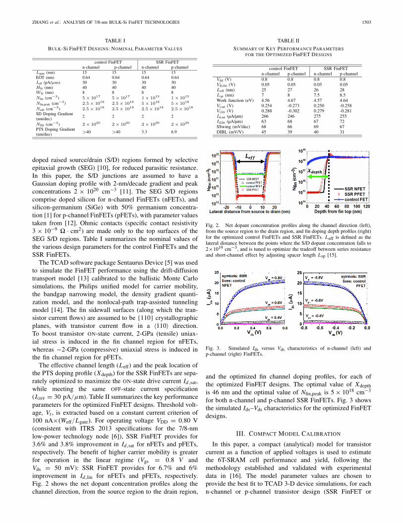
The effective channel length (Leff) and the peak location ofthe PTS doping profile (Xdepth) for the SSR FinFETs are sepa-rately optimized to maximize the ON-state drive current Id,sat,while meeting the same OFF-state current specification(IOFF = 30 pA/μm). Table II summarizes the key performanceparameters for the optimized FinFET designs. Threshold volt-age, Vt , is extracted based on a constant current criterion of100 nA×(Weff/Lgate). For operating voltage VDD = 0.80 V(consistent with ITRS 2013 specifications for the 7/8-nmlow-power technology node [6]), SSR FinFET provides for3.6% and 3.8% improvement in Id,sat for nFETs and pFETs,respectively. The benefit of higher carrier mobility is greaterfor operation in the linear regime (Vgs = 0.8 V andVds = 50 mV): SSR FinFET provides for 6.7% and 6%improvement in Id,lin for nFETs and pFETs, respectively.Fig. 2 shows the net dopant concentration profiles along thechannel direction, from the source region to the drain region,
TABLE II
SUMMARY OF KEY PERFORMANCE PARAMETERSFOR THE OPTIMIZED FinFET DESIGNS
Fig. 2. Net dopant concentration profiles along the channel direction (left),from the source region to the drain region, and fin doping depth profiles (right)for the optimized control FinFETs and SSR FinFETs. Leff is defined as thelateral distance between the points where the S/D dopant concentration falls to2×1019 cm−3, and is tuned to optimize the tradeoff between series resistanceand short-channel effect by adjusting spacer length Lsp [15].
Fig. 3. Simulated Ids versus Vds characteristics of n-channel (left) andp-channel (right) FinFETs.
and the optimized fin channel doping profiles, for each ofthe optimized FinFET designs. The optimal value of Xdepthis 46 nm and the optimal value of Nfin,peak is 5 × 1018 cm−3
for both n-channel and p-channel SSR FinFETs. Fig. 3 showsthe simulated Ids–Vds characteristics for the optimized FinFETdesigns.
III. COMPACT MODEL CALIBRATION
In this paper, a compact (analytical) model for transistorcurrent as a function of applied voltages is used to estimatethe 6T-SRAM cell performance and yield, following themethodology established and validated with experimentaldata in [16]. The model parameter values are chosen toprovide the best fit to TCAD 3-D device simulations, for eachn-channel or p-channel transistor design (SSR FinFET or
1504 IEEE TRANSACTIONS ON ELECTRON DEVICES, VOL. 63, NO. 4, APRIL 2016
Fig. 4. Comparison of the calibrated compact model (lines) and simulatedtransfer characteristics (symbols) for nFETs.
Fig. 5. Comparison of the calibrated compact model (lines) and simulatedtransfer characteristics (symbols) for pFETs.
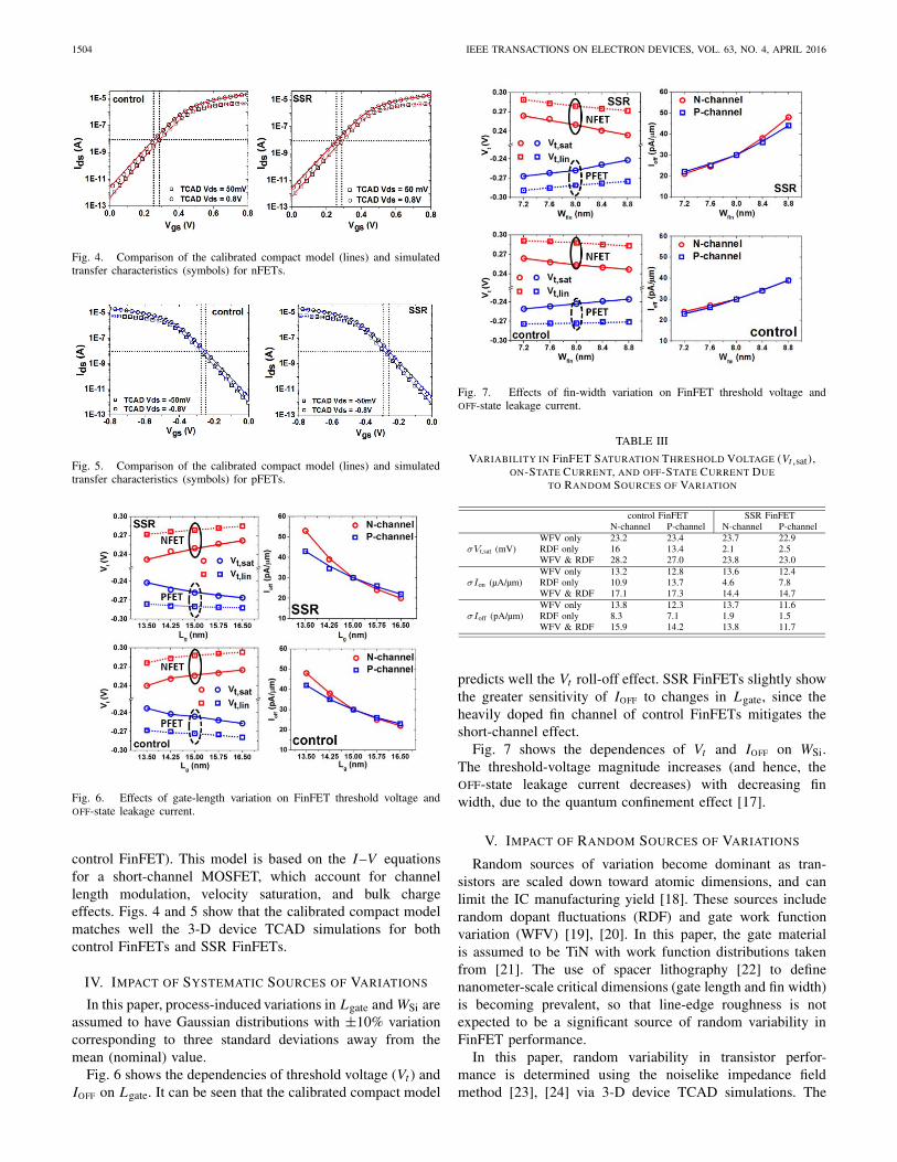
Fig. 6. Effects of gate-length variation on FinFET threshold voltage andOFF-state leakage current.
control FinFET). This model is based on the I–V equationsfor a short-channel MOSFET, which account for channellength modulation, velocity saturation, and bulk chargeeffects. Figs. 4 and 5 show that the calibrated compact modelmatches well the 3-D device TCAD simulations for bothcontrol FinFETs and SSR FinFETs.
IV. IMPACT OF SYSTEMATIC SOURCES OF VARIATIONS
In this paper, process-induced variations in Lgate and WSi areassumed to have Gaussian distributions with ±10% variationcorresponding to three standard deviations away from themean (nominal) value.
Fig. 6 shows the dependencies of threshold voltage (Vt ) andIOFF on Lgate. It can be seen that the calibrated compact model
Fig. 7. Effects of fin-width variation on FinFET threshold voltage andOFF-state leakage current.
TABLE III
VARIABILITY IN FinFET SATURATION THRESHOLD VOLTAGE (Vt,sat),ON-STATE CURRENT, AND OFF-STATE CURRENT DUE
TO RANDOM SOURCES OF VARIATION
predicts well the Vt roll-off effect. SSR FinFETs slightly showthe greater sensitivity of IOFF to changes in Lgate, since theheavily doped fin channel of control FinFETs mitigates theshort-channel effect.
Fig. 7 shows the dependences of Vt and IOFF on WSi.The threshold-voltage magnitude increases (and hence, theOFF-state leakage current decreases) with decreasing finwidth, due to the quantum confinement effect [17].
V. IMPACT OF RANDOM SOURCES OF VARIATIONS
Random sources of variation become dominant as tran-sistors are scaled down toward atomic dimensions, and canlimit the IC manufacturing yield [18]. These sources includerandom dopant fluctuations (RDF) and gate work functionvariation (WFV) [19], [20]. In this paper, the gate materialis assumed to be TiN with work function distributions takenfrom [21]. The use of spacer lithography [22] to definenanometer-scale critical dimensions (gate length and fin width)is becoming prevalent, so that line-edge roughness is notexpected to be a significant source of random variability inFinFET performance.
In this paper, random variability in transistor perfor-mance is determined using the noiselike impedance fieldmethod [23], [24] via 3-D device TCAD simulations. The

ZHANG et al.: ANALYSIS OF 7/8-nm BULK-Si FinFET TECHNOLOGIES 1505
Fig. 8. Modeled write-N curves (left) and butterfly curves (right) for the1-3-3 FinFET 6T-SRAM cell design. Iw is the minimum amount of currentflowing out of the internal storage node as it is discharged from VDD towardground potential. Read SNM corresponds to the length of the largest squarethat fits within the smaller lobe of the butterfly plot.
TABLE IV
COMPARISON OF FinFET-BASED 6T-SRAM CELL
PERFORMANCE METRICS (VDD = 0.80 V)
results summarized in Table III show that the SSR FinFETshave good immunity to RDF, since they have relatively lightdopant concentration within the (fully depleted) fin channelregion, so that the depletion charge negligibly affects thethreshold voltage. Note that the results show that WFV hasa dominant effect, which is consistent with the previous work,identifying WFV as the dominant contributor to Vt variationfor the FinFET technology [18]. Overall, SSR FinFETs areless susceptible to random sources of variation and, therefore,are promising for achieving higher IC manufacturing yield.
VI. 6T-SRAM CELL PERFORMANCE
The 6T-SRAM cell read stability and write ability aregauged by the read static noise margin (SNM) and write-ability current (Iw) [25] metrics derived from the butterflyplot and write-N curve generated using the calibrated modelmentioned above. The cell beta ratio is defined as the ratioof the n-channel pull-down (PD) transistor drive (ON-state)current to the n-channel pass-gate (PG) transistor drivecurrent. For the planar MOSFET technology, this ratio canbe finely tuned by adjusting the drawn channel widths of thePD and PG transistors. For the FinFET technology, it canonly be practically tuned coarsely by adjusting the number offins (connected in parallel between the source and the drainregions) in each device. Better read stability is achieved byusing more fins for the PD devices than for the PG devices.
Fig. 8 shows the modeled butterfly curves and write-Ncurves for the 1-3-3 FinFET 6T-SRAM cell design, whichcomprises one fin in each of the p-channel pull-up (PU)transistor, three fins in each of the PD device, and three finsin each of the PG device. Table IV summarizes the readSNM and Iw values for different cell designs. It can be seenthat the SSR FinFETs provide for better 6T-SRAM cell write
Fig. 9. Read SNM yield versus write-ability current yield, for the 1-2-1,1-2-2, and 1-3-3 SRAM cell designs comprising either SSR FinFETs (filledsymbols) or control FinFETs (open symbols). Cell operating voltage VDD isvaried from 0.38 to 0.80 V in 60-mV steps.
ability, because the gamma ratio (PG nFET to PU pFET drivecurrent ratio) for the SSR FinFET technology (1.08) is largerthan that for the control FinFET technology (1.06). The readSNM for the SSR FinFET technology is comparable to thatfor the control FinFET technology, since the cell beta ratiois determined by the ratio of the number of fins in the PDtransistor to the number of fins in the PG transistor, which isthe same for both technologies.
VII. 6T-SRAM YIELD ESTIMATION
Variability in transistor performance due to systematic andrandom sources of variation in the fabrication process canresult in a 6T-SRAM cell with read SNM <0 V or Iw < 0,which does not function properly, i.e., cell failure. Previouswork [19], [26] has shown that the threshold-voltage Vt
distributions caused by random sources of variations are closeto Gaussian. Cell sigma [16] is defined as the minimum totalnumber of standard deviations from the nominal value, forany combination of 18 device parameters (gate length, finwidth, and threshold voltage for each of the six transistors in a6T-SRAM cell), that causes a read disturb error or a writefailure. By assuming that 3σ deviation from the mean(nominal) value corresponds to ±10% variation for Lgate andfor Wfin, and accounting for random Vt variations due to WFVand RDF, the cell sigma is modeled in a multidimensionalvariation space.
Lower operating voltage is beneficial for reducing powerconsumption, but can result in lower nominal values of readSNM and/or Iw and, therefore, higher probability of cellfailure due to variations. The minimum cell operating volt-age (VDD,min) is defined as the lowest operating voltage forwhich the cell meets the six-sigma yield requirement (forSRAM arrays with greater than 256-Mb capacity) for bothread SNM and Iw.
The methodology established by [16] is used, herein, todetermine the read SNM and Iw cell sigma values, based

1506 IEEE TRANSACTIONS ON ELECTRON DEVICES, VOL. 63, NO. 4, APRIL 2016
TABLE V
COMPARISON OF MINIMUM OPERATING VOLTAGE (VDD,min)FOR VARIOUS FinFET-BASED 6T-SRAM CELL DESIGNS
on the sensitivities of these SRAM metrics to each deviceparameter. Fig. 9 directly compares cell sigmas for theSSR FinFET technology versus control FinFET technology,for the 1-2-1, 1-2-2, and 1-3-3 cell designs. Lowest Vdd,minis found to be 0.40 V and 0.46 V, respectively, for theSSR FinFET technology and the control FinFET technology.Table V summarizes Vdd,min for various SRAM cell designs.It shows that the 1-2-1 cell design has the worst VDD,mindespite having the best read SNM, as shown in Table IV.This is because VDD,min is actually limited by Iw cell sigmabecause stronger PU devices limit PG devices’ capability topull the internal node down to GND. The 1-2-2, 1-3-2, and1-3-3 cell designs implemented with the SSR FinFETtechnology are projected to be able to scale to operatingvoltages below 0.50 V.
VIII. CONCLUSION
An SSR fin channel doping profile enabled by oxygeninsertion technology is beneficial for improving deviceperformance (particularly Id,lin by 6.7% for nMOS andby 6% for pMOS) and for reducing the sensitivity of deviceperformance to process-induced variations. These benefitsare provided for superior write ability of 6T-SRAM cells,and are projected to facilitate reductions in the minimumcell operating voltage (by as much as 100 mV as comparedwith the conventional FinFET technology), to below 0.50 V.Noticeably, the 1-1-1 SSR FinFET cell design scales VDD,minto 0.50 V, comparable with the 1-3-2 control FinFETcell design. Notably, the 1-1-1 SSR FinFET cell design isprojected to allow VDD,min to be scaled down to 0.50 V,comparable with the larger 1-3-2 control FinFET cell design.Thus, the SSR FinFET technology can provide for 20%savings in SRAM cell area, based on the FinFET layoutdesign rules in [7] and [27]. This paper shows that the bulk-siFinFET technology can extend CMOS scaling beyond the10-nm node.
REFERENCES
[1] C. Auth et al., “A 22 nm high performance and low-power CMOStechnology featuring fully-depleted tri-gate transistors, self-alignedcontacts and high density MIM capacitors,” in Proc. Symp. VLSITechnol. (VLSIT), Jun. 2012, pp. 131–132.
[2] H. Bu, “FinFET technology a substrate perspective,” in Proc. IEEE Int.SOI Conf. (SOI), Oct. 2011, pp. 1–27.
[3] N. Xu et al., “Extension of planar bulk n-channel MOSFET scaling withoxygen insertion technology,” IEEE Trans. Electron Devices, vol. 61,no. 9, pp. 3345–3349, Sep. 2014.
[4] N. Xu et al., “MOSFET performance and scalability enhancement byinsertion of oxygen layers,” in Proc. IEEE Int. Electron Devices Meeting,Dec. 2012, pp. 6.4.1–6.4.4.
[5] Sentaurus Sdevice User’s Manual, Synopsys Inc, Mountain View, CA,USA, 2014.
[6] L. Wilson, International Technology Roadmap for Semiconductors(ITRS). Washington, DC, USA: Semiconductor Industry Association,2013.
[7] S. Natarajan et al., “A 14 nm logic technology featuring 2nd-generationFinFET, air-gapped interconnects, self-aligned double patterning and a0.0588 μm2 SRAM cell size,” in Proc. IEEE Int. Electron DevicesMeeting (IEDM), Dec. 2014, pp. 3.7.1–3.7.3.
[8] S.-Y. Wu et al., “A 16 nm FinFET CMOS technology for mobileSoC and computing applications,” in Proc. IEEE Int. Electron DevicesMeeting (IEDM), Dec. 2013, pp. 9.1.1–9.1.4.
[9] W. Xiong et al., “Improvement of FinFET electrical characteristicsby hydrogen annealing,” IEEE Electron Device Lett., vol. 25, no. 8,pp. 541–543, Aug. 2004.
[10] A. Hokazono, K. Ohuchi, K. Miyano, I. Mizushima, Y. Tsunashima,and Y. Toyoshima, “Source/drain engineering for sub-100 nm CMOSusing selective epitaxial growth technique,” in IEDM Tech. Dig., 2000,pp. 243–246.
[11] S. Sun et al., “Enable abrupt junction and advanced salicide formationwith dynamic surface annealing,” Phys. Status Solidi C, vol. 9, no. 12,pp. 2436–2439, 2012.
[12] M. V. Fischetti and S. E. Laux, “Band structure, deformation potentials,and carrier mobility in strained Si, Ge, and SiGe alloys,” J. Appl. Phys.,vol. 80, no. 4, pp. 2234–2252, 1996.
[13] M. G. Ancona and H. F. Tiersten, “Macroscopic physics of thesilicon inversion layer,” Phys. Rev. B, vol. 35, no. 15, pp. 7959–7965,1987.
[14] K.-H. Kao, A. S. Verhulst, W. G. Vandenberghe, B. Sorée,G. Groeseneken, and K. De Meyer, “Direct and indirect band-to-bandtunneling in germanium-based TFETs,” IEEE Trans. Electron Devices,vol. 59, no. 2, pp. 292–301, Feb. 2012.
[15] V. Vidya, “Thin-body silicon FET devices and technol-ogy,” Ph.D. dissertation, Dept. Elect. Eng. Comput. Sci.,Univ. California, Berkeley, Berkeley, CA, USA, 2007.
[16] A. E. Carlson, “Device and circuit techniques for reducing variation innanoscale SRAM,” Ph.D. dissertation, Dept. Elect. Eng. Comput. Sci.,Univ. California, Berkeley, Berkeley, CA, USA, 2008.
[17] S. Xiong and J. Bokor, “Sensitivity of double-gate and FinFET devicesto process variations,” IEEE Trans. Electron Devices, vol. 50, no. 11,pp. 2255–2261, Nov. 2003.
[18] T. Matsukawa et al., “Comprehensive analysis of variability sourcesof FinFET characteristics,” in Proc. Symp. VLSI Technol., 2009,pp. 118–119.
[19] X. Wang, A. R. Brown, B. Cheng, and A. Asenov, “Statistical variabilityand reliability in nanoscale FinFETs,” in Proc. IEEE Int. ElectronDevices Meeting (IEDM), Dec. 2011, pp. 5.4.1–5.4.4.
[20] H. F. Dadgour, K. Endo, V. K. De, and K. Banerjee, “Grain-orientation induced work function variation in nanoscale metal-gatetransistors—Part I: Modeling, analysis, and experimental validation,”IEEE Trans. Electron Devices, vol. 57, no. 10, pp. 2504–2514,Oct. 2010.
[21] X. Zhang et al., “Physical model of the impact of metal grain workfunction variability on emerging dual metal gate MOSFETs and itsimplication for SRAM reliability,” in Proc. IEEE Int. Electron DevicesMeeting (IEDM), Dec. 2009, pp. 1–4.
[22] C. Bencher, Y. Chen, H. Dai, W. Montgomery, and L. Huli, “22 nmhalf-pitch patterning by CVD spacer self alignment double pattern-ing (SADP),” Proc. SPIE, vol. 6924, p. 69244E, Mar. 2008.
[23] A. Wettstein, O. Penzin, E. Lyumkis, and W. Fichtner, “Randomdopant fluctuation modelling with the impedance field method,”in Proc. Int. Conf. Simulation Semiconductor Process. Devices, 2003,pp. 91–94.
[24] K. El Sayed, E. Lyumkis, and A. Wettstein, “Modeling statisticalvariability with the impedance field method,” in Proc. Int. Conf.Simulation Semiconductor Process. Devices (SISPAD), 2012,pp. 205–208.
[25] C. Wann et al., “SRAM cell design for stability methodology,” in Proc.IEEE VLSI-TSA Int. Symp. VLSI Technol. (VLSI-TSA-Tech), Apr. 2005,pp. 21–22.
[26] X. Wang, B. Cheng, A. R. Brown, C. Millar, and A. Asenov, “Statisticalvariability in 14-nm node SOI FinFETs and its impact on corresponding6T-SRAM cell design,” in Proc. Eur. Solid-State Device Res.Conf. (ESSDERC), 2012, pp. 113–116.
[27] M. Yabuuchi et al., “16 nm FinFET high-k/metal-gate 256-kbit6T SRAM macros with wordline overdriven assist,” in Proc. IEEE Int.Electron Devices Meeting (IEDM), Dec. 2014, pp. 3.3.1–3.3.3.
ZHANG et al.: ANALYSIS OF 7/8-nm BULK-Si FinFET TECHNOLOGIES 1507
Xi Zhang (SM’14) received the B.S. degree from theSchool of Physical Electronics, University of Elec-tronic Science and Technology of China, Chengdu,China, in 2013. She is currently pursuing thePh.D. degree in electrical engineering with theDepartment of Electrical Engineering and Com-puter Sciences, University of California at Berkeley,Berkeley, CA, USA.
Daniel Connelly (M’16) received the Ph.D. degreefrom Stanford University, Stanford, CA, USA.
He was involved in the advanced CMOS technol-ogy development at Acorn Technologies, La Jolla,CA, USA, and then in the device simulation andmodeling at Synopsys, Mountain View, CA, USA.He is currently a Visiting Scholar with the Universityof California at Berkeley, Berkeley, CA, USA.
Peng Zheng (S’11) received the B.S. degree inmicroelectronics from Tianjin University, Tianjin,China, in 2010, and the M.S. degree in electricaland computer engineering from the Georgia Insti-tute of Technology, Atlanta, GA, USA, in 2012.He is currently pursuing the Ph.D. degree in elec-trical engineering with the Department of ElectricalEngineering and Computer Sciences, University ofCalifornia at Berkeley, Berkeley, CA, USA.
Hideki Takeuchi (M’00) received the B.E. andM.E. degrees from The University of Tokyo, Tokyo,Japan, in 1988 and 1990, respectively.
He has been involved in the DRAM product devel-opment and various research projects on advancedCMOS, memories, and MEMS processes/devices.He is currently with Mears Technologies Inc.,Newton, MA, USA, where he is involved inprocess integration of the oxygen-insertiontechnology (MST) for various CMOS products.
Marek Hytha (SM’14) received the M.Sc. andPh.D. degrees in condensed matter physics fromCharles University, Prague, Czech Republic, in 1988and 1997, respectively.
He spent five years with Charles University, asan Assistant Professor. He has been with MearsTechnologies Inc., Newton, MA, USA, since 2003,where he is currently the Chief Scientist.
Robert J. Mears, photograph and biography not available at the time ofpublication.
Tsu-Jae King Liu (SM’00–F’07) received the B.S.,M.S., and Ph.D. degrees from Stanford University,Stanford, MA, USA, all in electrical engineering.
She is currently the TSMC Distinguished Pro-fessor of microelectronics with the Departmentof Electrical Engineering and Computer Sciences,University of California at Berkeley, Berkeley,CA, USA. Her current research interests includeenergy-efficient IC devices.