15 nanoscale intelligent materials and...
TRANSCRIPT

3430-8493-1653-X/01/$0.00+$1.50© 2005 by CRC Press LLC
15 Nanoscale Intelligent Materials and Structures
Yun Yeo-Heung, Inpil Kang, Sachin Jain, Atul Miskin, Suhasini Narasimhadevara, Goutham Kirkeria, Vishal Shinde, SriLaxmi Pammi, Saurabh Datta, Peng He, Douglas Hurd, Mark J. Schulz, Vesselin N. Shanov, Donglu Shi, F. James Boerio, and Mannur J. Sundaresan
CONTENTS
15.1 Introduction.................................................................................................34415.2 A Review of Smart Materials.....................................................................34915.3 Nanotube Geometric Structure...................................................................351
15.3.1 The Structure of Carbon Nanotubes ............................................35115.3.2 The Structure of Noncarbon Nanotubes ......................................35215.3.3 Designation of Nanotubes and Nanostructured Materials...........353
15.4 Mechanical and Physical Properties of Nanotubes....................................35515.4.1 Elastic Properties..........................................................................35515.4.2 Electrical Conductivity.................................................................35615.4.3 Magnetoresistance ........................................................................35715.4.4 Piezoresistance .............................................................................35715.4.5 Electrokinetics of Nanotubes .......................................................35815.4.6 The Piezoelectric Property ...........................................................35915.4.7 The Electrochemical Effect..........................................................36015.4.8 Nanotube Power Generation ........................................................36115.4.9 Nanotube Contact Phenomena.....................................................361
15.5 A Review of Different Types of Nanoscale Sensors and Actuators..........36315.5.1 Simulation of Nanotube Structures..............................................36315.5.2 Nanotube Strain Sensors ..............................................................36515.5.3 Actuators Based on Nanoscale Materials ....................................365
15.5.3.1 Carbon Nanotube Electrochemical Actuators ............36515.5.3.2 A Thermally Activated Actuator.................................36615.5.3.3 Piezoelectric and Nanotweezer Actuators ..................36615.5.3.4 Shape Memory Alloy and Platinum Nanoscale
Actuators .....................................................................36715.5.3.5 Biological Molecular Actuators..................................367
1653_C15.fm Page 343 Tuesday, December 21, 2004 3:44 PM
344 Nanoengineering of Structural, Functional, and Smart Materials
15.6 Manufacturing of Carbon Nanotube and Nanofiber Intelligent Materials .....................................................................................................36815.6.1 Synthesis of Nanotubes................................................................36815.6.2 Functionalization of Nanotubes ...................................................36915.6.3 Casting Nanotubes and Nanofibers in a Structural Polymer
Electrolyte.....................................................................................36915.6.4 Carbon Nanotube Composite Strain Sensors ..............................37115.6.5 A Carbon Nanotube–Based Biosensor ........................................37315.6.6 Carbon Nanotube and Nanofiber Hybrid Actuators ....................378
15.7 Future Directions for Intelligent Materials ................................................38515.7.1 A Carbon Structural Neural System............................................38515.7.2 High-Temperature Nanoscale Materials ......................................38815.7.3 Power Harvesting Using Carbon Nanotubes ...............................38915.7.4 Intelligent Machines.....................................................................39015.7.5 Telescoping Carbon Nanotubes ...................................................392
15.8 Conclusions.................................................................................................392Problems ................................................................................................................392Acknowledgments..................................................................................................393References..............................................................................................................393
15.1 INTRODUCTION
Since the time of the design of the lever and wheel, it has been a goal of mankindto improve the performance of engineered systems. To achieve large advances inthe performance of current systems—starting from the simplest machine elementsto automobiles, bridges, buildings, aircraft, helicopters, wind turbines, environmentalmonitoring systems, national security systems, and surgical and medical devices—will probably require that these systems become intelligent. Intelligent systems andmachines will be autonomous, self-sensing, able to resist vibration, redistributeloads, and change shape in response to their environmental conditions, and thereforepreserve their integrity, increase their life, optimize their performance, reduce thecost of ownership, and provide continuous safety during use. The critical ingredientneeded to make structures and machines intelligent is intelligent materials. Theproblem is that current intelligent materials have limited capabilities and new classesof practical and enabling intelligent materials with vastly improved properties areneeded. This chapter therefore tackles the problem of designing new intelligentmaterials and takes the approach of using nanoscale components and developingprocesses to build intelligent materials from the bottom up.
The terms intelligent and smart are often used rather interchangeably, and they candescribe both materials and structures. Smart materials are defined as having sensingor actuation properties such as a piezoelectric response to dynamic strain, which causeselectrons to move. Smart structures use smart materials for sensing and actuation inanalog or digital closed-loop feedback systems. Intelligent usually designates a morecomplex level of material behavior or control possibly by using miniaturized electronicsbuilt into the material itself or by using a more advanced feedback system such as a
1653_C15.fm Page 344 Tuesday, December 21, 2004 3:44 PM

Nanoscale Intelligent Materials and Structures 345
digitally controlled structure programmed with a rudimentary ability to learn and reason.Smart structures can also be passive such as a wing designed with bend-twistingcoupling to protect against flutter, or semiactive such as a magnetorheologic damperthat uses a feedback signal to control the voltage field and viscosity of a fluid. Smartmaterials and structures that are fully active use a feedback signal, processor, amplifier,and actuators to apply forces to control the vibration or shape of a structure.
Present smart/intelligent materials and structures have fundamental limitationsin their sensitivity, size, cost, ruggedness, and weight that have restricted theirwidespread application. To address the need for new intelligent materials and sys-tems, researchers are investigating nanotechnology and also intersecting nanotech-nology with biomimetics. Nanotechnology can provide the route to build perfectmaterials starting at the atomic scale, as in nature, while biomimetics can providethe inspiration and architecture for material system design. Multifunctionality is auniversal trait of biological materials and systems and is an important attribute whendeveloping intelligent materials and structures. Biological systems have beendesigned by nature from the smallest components upward over a long period of time,and they have material capabilities unmatched by manmade systems. The conceptof biologically inspired nanotechnology, or bionanotechnology, can be described asthe process of mimicking the chemical and evolutionary processes found in natureto synthesize unique almost defect-free multifunctional material systems startingfrom the nanoscale up. Bionanotechnology is thus a new frontier that can lead tonew generations of smart materials and intelligent systems that can sense and respondto their environment.
Although we are at an early stage of research, nanoscale intelligent materialsincluding carbon nanotubes, inorganic nanotubes, compound nanotubes, nanobelts,and other nanoscale materials have produced great excitement in the research com-munity. This is because of their remarkable and varied electrical and mechanicalproperties including electrical conductance, high mechanical stiffness, light weight,electron-spin resonance, electrochemical actuation, piezoelectricity, piezoresistance,contact resistance, Coulomb drag power generation, thermal conductivity, lumines-cence, and the possibilities for functionalizing these materials to change their intrinsicproperties. These attractive properties also have the potential for developing self-contained nanoscale intelligent materials based on analog or digital control of thematerial using built-in nanoscale electronics. The broad area of nanoengineering ofintelligent materials is discussed in this chapter, starting from material synthesis tothe processing of nanostructured hybrid materials and then fabrication of devicessuch as strain sensors, biosensors, and wet and dry actuators. The focus is onnanotube-based materials that have novel strain sensing and force actuation propertiesand the associated material processing steps needed to build macroscale materialsfrom nanoscale components, including digital control of the material behavior.Nanoscale smart materials are important because they often possess improved ordifferent properties from macroscale materials due to their near perfect construction,large surface area per volume, or quantum effects.1–12
While nanoscale materials and in particular carbon nanotubes (CNT) haveextraordinary properties, utilizing these properties at the nanoscale and at the mac-roscale is presenting major challenges for scientists and engineers. Thus far, nanoscale
1653_C15.fm Page 345 Tuesday, December 21, 2004 3:44 PM

346 Nanoengineering of Structural, Functional, and Smart Materials
intelligent materials have mostly been based on carbon nanotubes. A single-wallcarbon nanotube (SWCNT) is a superelastic crystalline molecule that can have alength-to-diameter ratio of 1000 or more, and an enormous interfacial area of500 m2/gm or more. Custom designing of multifunctional materials by mixing nan-otubes with bulk carrier materials is now producing a range of new properties suchas piezoresistivity and electrochemical transduction, as well as enhanced strength,modulus, toughness, hardness, and thermal and electrical conductivity, while simul-taneously decreasing thermal expansion and permeability. Obtaining and usingthese properties for smart materials is dependent on understanding the composition-topography-processing relationships that define nanomaterial behavior. Major diffi-culties in forming nanocomposite materials occur because CNT do not easily transferload to matrix materials because their small size can affect the molecular structureof the host material, and because van der Waals bonding is weak in the axial directionof the nanotubes and cannot prevent intertube longitudinal slipping. Also the van derWaals bonding is strong in the transverse direction, which makes it difficult totransversely separate and disperse the CNT. A consequence of this behavior is thatbundles of parallel nanotubes are difficult to pull apart transversely, but they canaxially slip and therefore can act as defects in polymer smart materials. Mechanicallyand chemically altering the nanotubes to disperse and to bond with the host materialis helpful, but this can adversely affect the electrical and transduction properties ofthe material. In addition, nanotube electrochemical actuators must allow ion conduc-tivity over the surface of the nanotube while simultaneously transferring actuationstrain to and from the nanotube. While many materials have the possibility forelectrochemical actuation, the effect is negligible in bulk materials because most oftheir atoms are in the interior. Conversely, in SWCNT all the atoms on are the surfaceand the electrochemical actuation effect is large. When the nanotubes collect in bundlesor ropes, the inner nanotubes are shielded from the ion exchange and the nanotubesalso slip on one another. Therefore, the critical factors in the design of nanotube intel-ligent materials, and especially electrochemical actuators, are that the nanotubes mustbe separated and aligned for electrical conductivity and ion exchange, and the strainmust be transferred from the nanotube to the host material. Otherwise macroscalenanotube intelligent materials and actuators will be weak and inefficient. There is alsothe possibility of using nanotube actuators at the nanoscale, but there is not muchresearch published in this new area.
In the broadest sense, the goal of nanoscale materials research is to developmultifunctional intelligent materials. These materials would possess high strain tofailure and high stiffness, be lightweight, and have a high bandwidth for actuationor sensing. They would provide a strong structural material that simultaneously hassensing, actuation, and other functional capabilities. There is no other smart materialavailable today that is also a structural material. Therefore nanotube hybrid actuatorand sensor materials could be an enabling technology for the improvement of allkinds of dynamic systems including helicopters, reconfigurable aerodynamic sur-faces, launch vehicles, ultra-high energy density wireless motors, and nanodevicessuch as biomedical nanosensors, surgical robots, active catheters, and biomedicalimplants. Nanotechnology is attractive and exciting because it might produce themost efficient smart materials ever made. On the other hand, nanoscience is presently
1653_C15.fm Page 346 Tuesday, December 21, 2004 3:44 PM
Nanoscale Intelligent Materials and Structures 347
difficult to put into applications. Various techniques for processing nanoscale mate-rials are presented in the literature, but many of these are difficult to extrapolate tothe macroscale or to use for large volume production due to the impracticality ofthe processing method or cost. Moreover some statements in the literature seem toinflate the potential of nanotechnology, which will lead to a backlash that willimpede nanotechnology research. Stating that carbon nanotubes are 100 timesstronger at one-sixth the weight of steel is misleading, because nanotubes are ananoscale orthotropic molecule and steel is an isotropic bulk material, and the twoare not directly interchangeable. It would be more realistic to compare the propertiesof a SWCNT with those of a typical commercial reinforcing fiber used today. InTable 15.1, the elastic properties of the Hexcel IM8 carbon fiber12 are compared tothe elastic properties of a SWCNT. The elastic modulus of the SWCNT is 3.3 timesgreater than the elastic modulus of the carbon fiber, and the specific modulus of theSWCNT is 4.4 times greater than the specific modulus of the carbon fiber. Thestrength of the SWCNT is 8.9 times greater than the strength of the carbon fiber,and the specific strength of the SWCNT is 12 times greater than the specific strengthof the carbon fiber. Also the elastic modulus of a unidirectional SWCNT-epoxycomposite is 3.2 times greater than the elastic modulus of a unidirectional carbonfiber-epoxy composite, and the specific modulus of a unidirectional SWCNT-epoxycomposite is 4.2 times greater than the specific modulus of a unidirectional carbonfiber-epoxy composite. Since a typical carbon fiber is a bulk material that is 3643 timeslarger in diameter than the SWCNT, there is a significant problem of processing thenanocomposite material to bring its nanoscale properties to the macroscale. Anotherseeming overstatement occurred in a New York Times article: “Today’s Visions ofthe Science of Tomorrow,” Jan 4, 2003. In the article, it was predicted that nano-technology will lead to aerospace vehicles with 98% less structural mass. It isinteresting to speculate how long it will take the aerospace companies to meet thisprediction.
On the positive side, there have recently been large advances in nanoscalematerials development. Small percentages of CNT are being incorporated into poly-mers, carbon fibers, and metals for reinforcement, and these hybrid materials haveshown significant improvements in elastic modulus or toughness, as compared to thehost polymer material. Spinning of fibers from carbon nanotubes has produced strongfibers that could be incorporated into polymers to produce super-strong materialswhen the cost of the fiber decreases. Electrochemical actuation in carbon nanofibercomposites has also been demonstrated, and this material could provide actuatorcapability to large structures. An important contribution of this chapter is to presentuseful approaches to tackle the problems of manufacturing nanoscale intelligentmaterials. Also presented are some ideas a little on the wild side for building futuristicintelligent structures, biodevices, and structural health monitoring systems. Readersshould also pay attention to nonstructural and smaller material volume applicationsfor nanoscale intelligent materials including biosensing, surgical manipulators, andsmart machines, which are also discussed in the chapter. One such idea for applicationsis a fluid form of an intelligent material that may have properties that can be activatedby contact with another material. There are potentially many types of nanotube-basedfluids that take advantage of the small size and ability to functionalize nanotubes.
1653_C15.fm Page 347 Tuesday, December 21, 2004 3:44 PM

348 Nanoengineering of Structural, Functional, and Smart Materials
TAB
LE 1
5.1
Prop
erti
es o
f R
einf
orci
ng F
iber
s an
d Th
eir
Com
posi
tes
wit
h 62
% F
iber
Vol
ume
Frac
tion
Mat
eria
lD
iam
eter
D [
nm]
Den
sity
d [k
g/m
3 ]St
rain
to F
ail
[%]
Mod
ulus
Y
[GPa
]Sp
ecifi
c M
odul
us[Y
/d]
Ult
. St
reng
th S
[GPa
]Sp
ecifi
c St
reng
th[S
/d]
SWC
NT
Fib
er [
1]1.
413
40>1
0∼1
000
0.74
6∼5
037
.3e−3
Hex
cel I
M8
Car
bon
fibe
r [1
2]51
0017
902
304
0.17
5.58
93.
12e−3
Rat
io fi
bers
SW
CN
T/I
M8
1/36
430.
75>5
3.3
4.4
8.9
12E
poxy
—11
217
3.2
0.00
290.
083
7.4e
−5
SWC
NT-
Epo
xy—
1252
—∼5
62 (
calc
)0.
48—
—IM
8 Fi
ber-
Epo
xy—
1537
—17
6 (m
eas)
0.11
52.
761.
8e−3
Rat
io S
WC
NT-
Epo
xy/I
M8
Epo
xy—
0.81
5—
3.2
4.2
——
1653_C15.fm Page 348 Tuesday, December 21, 2004 3:44 PM
Nanoscale Intelligent Materials and Structures 349
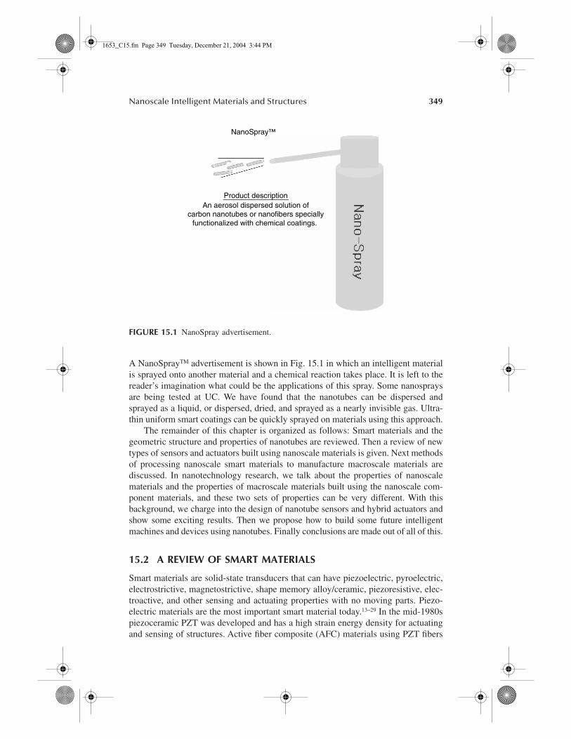
A NanoSprayTM advertisement is shown in Fig. 15.1 in which an intelligent materialis sprayed onto another material and a chemical reaction takes place. It is left to thereader’s imagination what could be the applications of this spray. Some nanospraysare being tested at UC. We have found that the nanotubes can be dispersed andsprayed as a liquid, or dispersed, dried, and sprayed as a nearly invisible gas. Ultra-thin uniform smart coatings can be quickly sprayed on materials using this approach.
The remainder of this chapter is organized as follows: Smart materials and thegeometric structure and properties of nanotubes are reviewed. Then a review of newtypes of sensors and actuators built using nanoscale materials is given. Next methodsof processing nanoscale smart materials to manufacture macroscale materials arediscussed. In nanotechnology research, we talk about the properties of nanoscalematerials and the properties of macroscale materials built using the nanoscale com-ponent materials, and these two sets of properties can be very different. With thisbackground, we charge into the design of nanotube sensors and hybrid actuators andshow some exciting results. Then we propose how to build some future intelligentmachines and devices using nanotubes. Finally conclusions are made out of all of this.
15.2 A REVIEW OF SMART MATERIALS
Smart materials are solid-state transducers that can have piezoelectric, pyroelectric,electrostrictive, magnetostrictive, shape memory alloy/ceramic, piezoresistive, elec-troactive, and other sensing and actuating properties with no moving parts. Piezo-electric materials are the most important smart material today.13–29 In the mid-1980spiezoceramic PZT was developed and has a high strain energy density for actuatingand sensing of structures. Active fiber composite (AFC) materials using PZT fibers
FIGURE 15.1 NanoSpray advertisement.
NanoSpray™
Product descriptionAn aerosol dispersed solution of
carbon nanotubes or nanofibers speciallyfunctionalized with chemical coatings.
1653_C15.fm Page 349 Tuesday, December 21, 2004 3:44 PM

350 Nanoengineering of Structural, Functional, and Smart Materials
were developed in 199721–23 by Hagood and Bent at MIT. In 2000, a variation ofthis material was developed by NASA, called the macrofiber composite (MFC).24
The AFC/MFC material is built using parallel piezoceramic fibers or ribbons in anepoxy matrix with an interdigitated electrode pattern on the top and bottom facesof the composite layer, but not touching the fibers. At the University of Cincinnati(UC), the construction of the AFC material was modified to develop piezoelectricartificial nerves for sensing of structures.25 While AFC represent a large advance inthe development of high-impedance smart materials, the AFC are still relativelyheavy and only partially load bearing, there is a strength mismatch between the AFCand host material, and their strain is ∼0.2%. These are significant limitations whendeveloping smart structures for advanced applications. There has been progress indeveloping higher strain single crystal piezoelectrics, relaxor ferroelectrics, andalkaline-based piezoelectric materials, but the processing methods for these materialsare not yet scalable to commercial quantities, and the brittle heavy nature of thematerials remain.
In 1991, multiwall carbon nanotubes (MWCNT) were discovered by SumioIijima,30 and since then carbon nanotube synthesis has been intensely studied.31–34
Also see Part 1 of this book for current research in nanotube growth. In 1996 theC60 fullerene and SWCNT were synthesized by Richard Smalley et al. 32 CouplingCNT to electronic circuits was then studied as in References 35–43. In 1999,electrochemical actuation of SWCNT was developed by Ray Baughman et al.44–68;in 2000–2001 CNT ropes and aligned membranes were developed;69–72 in 2001composite materials strengthened with CNT were studied by methods includingRaman scattering73–90; and in 2001 the piezoelectric effects in carbon nanotubes(CNT), boron nitride nanotubes (BNT) 91–95 (also see Chapter 21 of this book) andsilicon nitride nanotubes were studied.96–100 Silicon oxide and vanadium oxidenanotubes were also studied. In 2002 electrochemical actuation of a single carbonnanotube was studied49,54 and improvements in CNT actuation58 were made, andin 2003 vanadium oxide nanotubes (VNT) were used for actuation.98 Zinc oxidenanobelts that have piezoelectric properties are discussed in Reference 100 and inChapter 4 of this book. Noncarbon nanotubes are discussed in References 101–114,and piezoelectric and other nanotubes are discussed in References 115–121. Nanotubeelectronic properties are given in References 122–135. These research efforts haveverified that CNT-, VNT-, and BNT-based materials have extraordinarily highstrength, super-elasticity, and sensing capability, all at the same time. These propertiesmake nanotubes possibly the material of choice for designing future smart materialsand strain actuators. However, BNT are not readily available yet and they havepiezoelectric strain coefficients (dij) that are perhaps 20 times lower than existingpiezoelectric ceramic materials, and it is not possible to separate the chiralities ofBNT. VNT have lower actuation properties than CNT, but their cost is projected tobe lower. Zinc oxide nanobelts may have good piezoelectric properties and strength,but they are not commonly available or used in composites yet. Because the BNT,VNT, and zinc oxide materials may have lower strain than electrochemical CNT, andthe materials are not as well developed, their potential as a bulk smart material seemsnot yet as promising as CNT, depending on the application. Hopefully piezoelectricnanoscale materials will become more available soon.
1653_C15.fm Page 350 Tuesday, December 21, 2004 3:44 PM
Nanoscale Intelligent Materials and Structures 351
Based on theory, CNT have large electrochemical actuation properties. In practice,bringing these properties to the macroscale is difficult. Transferring charge to thetubes in a SWCNT actuator and transferring the shear load through the actuator havebeen limitations to realizing the theoretically predicted ∼2% strain and high perfor-mance of SWCNT actuators/sensors. Also Ray Baughman and his group at theUniversity of Texas at Dallas and Matteo Pasquali and his group at Rice Universityin Houston (Chapter 11) have described great progress in spinning CNT fibers. Thespun fibers are microns in diameter and the strength is greatly improved comparedto previous CNT fibers. A trade-off of strong fibers is that the nanoscale actuationproperties may be reduced compared to individual nanotubes because it is difficultto intercalate ions into the interior of the dense fibers.
To overcome the limitations of present smart materials and actuators, carbonnanotube hybrid materials are being developed at UC with a focus on minimizingion blockage and shear lag, and increasing the electrochemical process velocity andbandwidth of the material. This CNT hybrid smart material and the fiber-basedapproaches mentioned are anticipated to enable new material systems with applica-tions in mechatronic devices and large structures for defense and civilian systems.Unlike other smart materials, these CNT hybrid materials and fibers can be uniquebecause they are simultaneously structural, functional, and smart materials. The CNThybrid material is predicted to have a large load-carrying capability, and high thermaland electrical conductivity, actuation, and sensing properties. For design use, math-ematical models of the CNT material must be developed in terms of the electro-chemical constitutive equations for a composite material using a solid polymerelectrolyte (SPE) matrix. In preliminary work at UC, small CNT electrochemicalactuator material, a strain sensing material, and a power generation material havebeen built. Moreover a multiwall carbon nanofiber (CNF) PMMA electrochemicalactuation material has been tested that has good actuation performance and is about200 times lower in cost than a SWCNT actuator material. Development of aSWCNT/MWCNT/CNF-Epoxy-SPE material that is a high-performance structuralload bearing material that actuates and senses is the holy grail of the researchdescribed in this chapter. If successful, it would provide actuation and sensingcapabilities (i.e., intelligence) to large structures.
15.3 NANOTUBE GEOMETRIC STRUCTURE
The geometry of different types of nanotubes is briefly described in this section.The geometry plays an important role beyond the elastic properties—the geometryalso defines the electronic properties of the nanotube and affects the sensing andactuation properties of the smart material. Detailed nanotube mechanics are dis-cussed in References 136–142, and in Part 3 of this book.
15.3.1 THE STRUCTURE OF CARBON NANOTUBES
The crystal structure of graphite is a layered structure and the carbon atoms withina layer are strongly bound to their neighbors at room temperature, but the layers areonly loosely coupled by van der Waals forces, which makes graphite quite easily
1653_C15.fm Page 351 Tuesday, December 21, 2004 3:44 PM

352 Nanoengineering of Structural, Functional, and Smart Materials
deformable in a particular direction. This is why graphite is used as the core ofpencils and for dry lubricants. Although nanotubes grow axially, a SWCNT can bemost easily described as a rolled-up tubular shell of graphite sheet with the carbonatoms covalently bound to their neighbors. The bonding mechanism in a carbonnanotube system is similar to that of graphite, which is sp2 hybridization. One of theproperties in sp2 hybridization is the occurrence of s-bonds and p-bonds. The s-bondsare a strong covalent bond that binds the atoms in the plane and results in the highstiffness and high strength of a CNT. On the other hand, the p-bond is the interlayerinteraction of atom pairs and is much weaker than the s-bonds. One of the excitingproperties of nanotubes relates to their electronic band structure, which depends onthe helicity and diameter of the nanotube. The armchair nanotubes are metallic,whereas the zigzag and chiral tubes can be either metallic or semiconducting. Theseresults are major driving forces in the evolution of nanoelectronics including piezore-sistance of nanotubes,143–147 electrophoresis and dielectrophoresis of nanotubes,148–156
and carbon nanotube flow sensors.157–158 Functionalization is the chemical alterationof the surface properties of nanotubes for the purpose of improving adhesion to amatrix and improving the sensing165–177 and actuation properties of nanotubes.44–68
Apart from unique electronic properties, mechanical characteristics have providedexcitement because they include high strength, high stiffness, low density, superelas-ticity, and structural perfection. These remarkable multifunctional properties of CNThave the potential to be used as smart materials for reinforcing, sensing, and actuatingpolymer composites.
15.3.2 THE STRUCTURE OF NONCARBON NANOTUBES
Nanotube materials can be categorized as organic (e.g., carbon and various peptides)and inorganic (e.g., silicon nitride, boron nitride) nanotubes. Inspired by the remark-able functions of tubular structures in biology, much research in organic nanotubeshas focused on the biological functions in vivo and synthesis of various organicnanotubes for in vitro environments.178–191 Special attention in organic nanotubes isneeded to understand noncovalent processes of tubular materials such as lipic,peptidic, or steroidic systems. Since organic nanotubes have remarkable functionsin biology, researchers have been trying to understand the role of organic nanotubesand synthesize them in vitro. These organic nanotubes were studied for biosensorapplications. In addition, remarkable functions of organic nanotubes (e.g., motorproteins) can inspire researchers and may produce new types of biomimetic nanotubestructures for sensors and actuators in the near future.191
The small size, high strength, and remarkable physical properties of CNT areattractive, but nanotube properties depend on their diameter, thickness, helicity, anddefects, and the random helicity and high synthesis cost for purified samples arebarriers to applications. Therefore, researchers are increasingly investigating non-CNT materials or inorganic nanotubes and nanotubes of different inorganic mate-rials. Using our understanding of CNT phenomenona as a background, the extraor-dinary properties of inorganic nanotubes can be predicted in such examples asBxCyZz,, and dichalcogenides of transition metals including MeS2 (Me = Mo,W, Nb,S = S, Se,Te), MoO3, SiO2, Al2O3,V2O5, TiO2, NiCl2, InS, and Bi.147–154 Also lead
1653_C15.fm Page 352 Tuesday, December 21, 2004 3:44 PM

Nanoscale Intelligent Materials and Structures 353
titanate (PbTiO3, PT), lead zirconate (PbZrO3, PZ), and lead zirconium titanate(PbZrO3-PbTiO3, PZT) solid solution nanotubes were synthesized by a chelate sol-gel method.110 These inorganic nanotubes and compound nanotubes can compensatethe lack of control of chirality and properties of smart carbon nanotube structuresmaking it possible to modify the electrical, optical, mechanical, charging pattern,and other properties of nanotubes over a wide range.115–121 Therefore we cannotexempt the likelihood of using inorganic nanotubes for developing smart materials.In particular, the piezoelectric properties of boron nitride nanotubes (BNT) wereevaluated by calculating the polarization of a nanotube by the MNDO (neglect ofdiatomic differential overlap) method, which is a semiempirical method for thecalculation of molecular polarizabilities and hyperpolarizability. All types of dichal-cogenide nanotubes remain semiconducting even at the smallest diameters, andBNT are dielectric or semiconducting (n- or p-doped). Generally the width of theband gap increases as the diameter of the NT increases, but in the case of BNTand MeS2, the band gap remains constant. Another interesting feature of heteropolarnon-CNT nanotubes is the charge transfer resulting in ionic interatomic bonding.Compared to CNT, these non-CNT nanotubes are of great interest and are enlargingthe research field. More broad research not only in synthesis but also in propertiesdetermination of inorganic nanotubes and their properties in bundles and in poly-mers is needed to develop useful smart materials.
15.3.3 DESIGNATION OF NANOTUBES AND NANOSTRUCTURED MATERIALS
Many types of nanotubes are being developed, and the terminology used to describethem is not universal. Therefore, a list of some of the different types of nanotubesand nanofibers is given in Table 15.2, with references. The acronym for a carbonnanotube is CNT. The number of walls is described as single wall (SW), doublewall (DW), and multiwall (MW). The nanotube may be amorphous or crystalline.Bamboo nanotubes have internal closeouts along the length of the tube and thisoccurs in boron nitride nanotubes (BNT) and in some MWCNT due to the growthmechanism. There are also carbon nanofibers (CNF), which are different fromMWCNT because in the nanofiber the graphene walls are not parallel to the fiberaxis. They are at an angle of 20° in a Dixie cup arrangement and terminate in groupsat the outer wall of the fiber. This produces a rough surface and also exposes theends of the tubes to the surface, which may affect their electrical conduction andelectrochemical properties. SWCNT have one wall and diameters of about 1.4 nm;MWCNT have multiple concentric parallel walls and diameters of 10 nm and larger;CNF have multiple concentric parallel walls at an angle to the fiber axis and havediameters of 70 nm or larger. For comparison, graphite fibers used in traditionalcomposite materials have diameters on the order of 6000 nm.
Some of the important differences in the nanotubes/nanostructures are discussednext. There are also other nanostructured materials including nanobelts, nanohorns,nanoribbons, nanowires, nanoplates, nanonails, etc. that are not common and aremostly under development. The type of nanotube affects the processing method forsmart materials; SWCNT are the smallest diameter and the most difficult to process
1653_C15.fm Page 353 Tuesday, December 21, 2004 3:44 PM

354 Nanoengineering of Structural, Functional, and Smart Materials
into smart materials and the most expensive. MWCNT do not have as high or variedproperties but are easier to process because of their larger diameter (∼20 nm dia.).CNF are similar to MWCNT but there is a critical difference: The nanofibers arenot continuous tubes and their surfaces show steps at the termination of the wallsof groups of fibers. The nanofibers include PR 24 HT (∼70 nm dia.) and the PR 19(~130 nm dia.). The PR 19 has a CVD layer with a graphitic nature and these fibersmay be more robust to breakage, but the electrical properties of the nanofiber arechanged by the carbon coating. The PR-24 do not have a CVD coating. There arelow- and high-density variations of these two nanofiber types. More informationcan be obtained from the manufacturer.3 There are three main types of carbonnanotube raw materials that have potential for use as electrochemical actuators andsmart materials: (1) SWCNT, which have excellent electrochemical properties. Thecost, however, is very high, ∼$500/gm, and incorporating the nanotubes into poly-mers at high loadings is difficult. (2) MWCNT, which have good electrochemicalproperties. The cost is high, ∼$150/gm bulk or $1000 for a 1 cm2 array, andincorporating the nanotubes into polymers might be done by growing arrays ofnanotubes and casting the polymer around the arrays. (3) The PR-24 CNF. Theelectrochemical properties are good, the cost is low, ∼$0.25/gm, and incorporatingthe nanofibers into polymers is easier because the fibers are large. All three materialsseparately and in combination are being used at the UC to develop intelligentmaterials. SWCNT can be purchased commercially1–2 or can be grown using acommercial nanofurnace5; MWCNT can be purchased commercially2 and alsogrown in arrays5; and CNF can be purchased commercially.3 A nanotube synthesis
TABLE 15.2Designation of Nanotubes
Description and Sources
SWCNT: 0.3–2 nm D, 200–1000 nm L; grown by catalyzed CVD and other methods; cost purified is ∼$500/gram [1,10,13]
DWCNT: 2–4 nm D, 1–50 micron L; grown by CVD of methane over cobalt nanoparticles supported on porous MgO nanoparticles [2,12]
MWCNT: 10–50 nm D, 1–50 micron L; grown by CVD; also bamboo MWCNT 20–40 nm D, 1–20 micron L, internal closeouts [2,10]
Carbon Nanofiber, Pyrograf III trade name (CNF): 70–200 nm D, 50–100 micron L; nonconcentric nested tubes with walls angled 20° to the longitudinal axis, carbon crystal structure, produced as a vapor by decomposing hydrocarbons with a catalyst, hydrogen sulfide, and ammonia, different grades; cost ~$100/lb [3]
Boron Nitride Nanotubes (BNT): 3–40 nm D, 40–80 nm D bamboo/cone nanotubes and nanosize polyhedral particles in clusters [15]
Silicon Carbide Nanotubes (SiCNT): 200 nm D, 60 micron L, amorphous nanocrystalline [11,141–142]
SiOx Nanostructures: 20–30 nm D tubes, bundles, amorphous, thermal evaporation [2]
Vanadium Oxide (V2O5) Nanotubes (VNT): 15–100 nm D, MW [144]
1653_C15.fm Page 354 Tuesday, December 21, 2004 3:44 PM
Nanoscale Intelligent Materials and Structures 355
laboratory using chemical vapor deposition (CVD) is a feasible way to makenanotube materials for experimental purposes, (See Chapter 5). The differences innanotubes affect the processing and performance of the smart material. The dis-persion and functionalization processes depend on the type of nanotube. Dispersionof the nanotubes, preventing reagglomeration during curing, and the effect thenanotubes have on the polymer structure may be the most critical part of integratingany of the types of nanotubes into polymers.
15.4 MECHANICAL AND PHYSICAL PROPERTIESOF NANOTUBES
Because of the great properties of nanotubes, smart materials developed usingnanotubes have the potential to improve the way we generate and measure motionin devices from the nano- to the macroscale in size. The advantages of using SWCNT,MWCNT, and CNF are discussed here for building smart materials. One importantproperty that is ideal for all CNT materials is the ability to functionalize (chemicallymodify the surface of ) the CNT and alter its properties. SWCNT properties arediscussed in the next section relative to forming CNT hybrid actuators and sensors.In general, the elastic and transduction properties are the greatest for SWCNT. Theproperties decrease somewhat for MWCNT and decrease further for PR-24 CNF.Finally graphite fibers have almost no actuation properties, although they can beused as an electrical resistance–based sensor.
15.4.1 ELASTIC PROPERTIES
The Young’s modulus of SWCNT is as high as 1 terapascal. Compared withaluminum, steel, or titanium, the strength-to-weight ratio of nanotubes in theaxial direction is much greater. Compared to a composite with carbon fibers, thetheoretical specific modulus of a SWCNT composite may be about four timesgreater, as shown in Table 15.1. The maximum strain of SWCNT is 10% or more,which is higher than most high-strength structural materials. All of these strongmechanical properties are due to the C-C covalent bonding and the seamlesshexagonal network. Thermal conductivity is also very high in the direction of thenanotube axis. The mechanics of nanotubes is discussed in detail in Part 3 of thisbook. The incorporation of nanotubes into polymers can initiate multifunctionalimprovements in the following areas with industrial applications in parentheses:(1) increased physical strength (in aircraft and engine structural components);(2) increased vibration damping (in aircraft structures, brake disks); (3) resistanceto surface wear and scratching (in brake disks, leading edge components inaircraft, paint); (4) higher stiffness and dimensional stability (space structuresand structural components); (5) increased thermal conductivity (for use in brakes,engines, spacecraft, electronics heat sinks, PWBs); (6) EMI shielding (defenseelectronics); (7) energy harvesting from active nanocomposites (future applicationfor spacecraft, biomedical, communication); (8) increased fracture resistance (brakedisks, due to FOD in engines); (9) increased actuation performance (future applica-tion of morphing of wings); (10) sensing for health monitoring (future application
1653_C15.fm Page 355 Tuesday, December 21, 2004 3:44 PM

356 Nanoengineering of Structural, Functional, and Smart Materials
with carbon-based structural neural system at the UC); (11) corrosion and erosionresistance (aircraft edges); (12) clear nanocoatings and materials (on anodized/aluminum/polished surfaces, windows); (13) increased electrical conductivityand photoluminescence (in flight vehicles); and (14) actuation of structures(shape changing).
15.4.2 ELECTRICAL CONDUCTIVITY
Electronically the carbon nanotube can be either metallic or semiconducting. Carbonnanotubes also have been shown to conduct current balistically without dissipatingheat. In theory, there are two propagating eigenmodes for a SWCNT. Mismatch ofthe eigenmodes between the nanotube and a mechanical conductor makes electricalcontact difficult and high contact resistance may occur. The conductance (theinverse of resistance) of SWCNT is predicted to be 2G0 independent of the diameterand length, where G0 = 2e2/h = 1/12.9 kΩ, which is one unit of the conductancequantum, and e and h are the charge on one electron and Plank’s constant, respec-tively. This means that SWCNT are predicted to have a minimum resistance ofabout 6500 ohms, independent of their length. Temperature and magnetic fieldsaffect the resistance of the nanotubes. Metallic SWCNT behave as long ballisticquantum conductors with the charge carriers exhibiting a large phase-coherencelength. The semiconducting nanotubes are predicted to have the strongest electro-chemical properties, but this is difficult to verify in macroscale actuators. Theproperties of the nanotubes in a structural polymer electrolyte (SPE) define theelectrical and ion exchange, and actuation performance. The metallic or semicon-ducting properties of SWCNT actually depend on their helicity or chirality, whichis denoted by a pair of integers (n, m). In particular, they are predicted to be metallicif n − m = 3q, where q is an integer. While armchair CNT are metallic, electricalproperties of chiral and zigzag CNT vary with the diameter. Therefore rational designof nanotube smart structures requires a fundamental understanding of the conductiveproperties of nanotube materials and how conductivity depends on temperature anddimensionality.122–123 Based on recent observations of electron transport and boththeoretical and experimental results, SWCNT are ballistic in nature, implying theabsence of inelastic scattering.125 Experimental results of metallic SWCNT exhibitedresistance below 100 kΩ at room temperature, approaching the theoretical lower limitof 6.5 kΩ .126
Transport in MWCNT is controversial regarding ballistic and diffusive con-ductivity.172 In experiments, Bachtold et al. showed that resistance per unit lengthof MWCNT is above 5 kΩ/µm, resulting in diffusive conductivity.122 Frank et al.demonstrated that conductivity of MWCNT is ballistic and transport was confinedto the outer layer of the tube. 128 C. Gerger et al. reported that resistance of MWCNTis at most 200 Ω/µm. This implies that MWCNT conductivity is ballistic withalmost a 30-µm mean free path. The most interesting result is that only the surfaceof MWCNT transport current, and high current densities can be applied.129–130
Since our interest is in macroscopic smart nanotube structures, the conductivityproperties of SWCNT and MWCNT must be brought to the microscale or mac-roscale in the form of composites. Then the transport features of CNT composites
1653_C15.fm Page 356 Tuesday, December 21, 2004 3:44 PM

Nanoscale Intelligent Materials and Structures 357
can be considered for optimal design of nanotube smart materials.132–133 In ropes orbundles of SWCNT, or in mats consisting of randomly oriented ropes, the resis-tance increasing with temperature has been observed. M. Radosavljevic et al. foundthat the coupling between nanotubes in the bundle is weak, and the current iscarried predominantly by nanotubes on the surface of the bundle at low fields.134
At high bias voltage just before complete breakdown, they observed an additionalcurrent increase that was caused by the coupling to the nanotubes in the interiorof the bundle. These results indicate that nanotubes that are bundled may havedifferent transduction properties compared to individual nanotubes.
15.4.3 MAGNETORESISTANCE
The CNT also have spin-dependent transport properties or magnetoresistance. Thedirection of magnetization of the ferromagnetic electrodes used to contact the nan-otube defines the spin direction of the charge carriers into and out of the nanotubeand a change in the resistivity of the nanotube. Spintronic nanoscale devices in theorycan be built using the superconductivity and magnetoresistance effects, where thenanotube-metallic junction appears to have a strong effect on the spin-dependenttransport. When a magnetic field is applied perpendicularly to the nanotube, at lowtemperature, the resistance shows a change of 15%. Also a strongly suppressed con-ductance gap at zero bias voltage on a substrate can open at low temperature (4.2 K).The magnetoresistance effect would be difficult to measure for sensing/actuationof strain of the nanotube and for use in a smart material.
15.4.4 PIEZORESISTANCE
Piezoresistance is the change in electrical resistance with strain and is a usefulproperty for self-sensing of intelligent structures. Piezoresistance is discussed inReferences 143–147. A pioneering experiment showed that the conductance of ametallic CNT could decrease by orders of magnitude when strained by an atomicforce microscope tip.147 It was shown that the band structure of a CNT can bedramatically altered by mechanical strain and the conductance of the CNT canincrease or decrease depending on the chirality of the nanotube. This happensbecause the strain changes the structure of the quantum states available to theelectrons. Metals conduct electricity easily because their electrons have easy accessto the quantum states that carry the electrons long distances. These states are in theconduction band of the electronic structure. In semiconducting nanotubes, there isa band gap that is an energy barrier that electrons must overcome to reach theconduction band. The extra energy push to overcome the band gap can come fromheat or an electric field or strain. Actually strain changes the band structure, whichchanges the electrical properties making the nanotube or nanocomposite materialmore or less conductive (piezoresistive), depending on the chirality of the nanotubeand the polymer and percent loading of the nanotubes.80,82
Raman spectroscopy is a very useful tool to characterize carbon materialsbecause it gives information about the size of graphite crystallites and the degree ofordering of the material.166 Of particular importance, Raman shifts can represent all
1653_C15.fm Page 357 Tuesday, December 21, 2004 3:44 PM
358 Nanoengineering of Structural, Functional, and Smart Materials
types, shapes, and orientations of nanotubes. Therefore, Raman spectroscopy wasused to study the vibrational modes of carbon nanotubes and nanoropes and todetermine the characteristic properties of armchair, zigzag, and chiral tubes. It isalso reported that a polymer embedded with low-weight fractions of carbon nano-tubes becomes Raman-active under an applied mechanical strain. Small amounts ofSWCNT embedded in a polymer matrix were used to sense the mechanical responseof the polymer using Raman spectral data. The polarized Raman methods were avery useful tool to map the stress in a polymer plate under uniaxial tension. Thiscould be one way to sense in a smart structure, but there is still a limitation sincethe large and expensive Raman spectroscope instrument is required.
The electronic and mechanical degrees of freedom are tightly coupled in theCNT system. Many researchers try to prove how bond stretching and twisting innanotubes affects the electrical properties of nanotubes, since the electromechanicalproperties of SWNT depend on nanotube chirality (m, n). These properties havebeen exploited to sense mechanical deformations by a change in conductance orresistance of the nanotube due to the potential application for nanoscale smartstructures such as NEMS devices. Several groups calculated conductance variationsdue to mechanical deformation theoretically. Even for small bending angles, theconductance changed, and the conductance of metallic SWCNT was lowered up totenfold at the ∼45° bending angle.147 Experimental investigation of nanotubes wascarried out with suspended nanotubes that were manipulated with an AFM tip whilethe resistance or conductance was being monitored. 147 Conductance of the SWCNTdecreased each time the AFM tip pushed the SWCNT down but recovered as thetip retracted. These observed changes are entirely due to the mechanical elasticdeformation of the SWCNT. This phenomenon can be explained by the changes inlocal bonding configuration from sp2 to nearly sp3. As the AFM tip pushes theSWCNT down, local p-electron density is decreased significantly. Drastic reductionin p-electron density causes the significant decrease in conductance, because localp-electron density, which is delocalized, is responsible for the electrical conduction.Reversibility in the process and the dramatic variation in conductance are goodproperties to serve as reversible electromechanical transducers for smart structures.In particular, Z.L. Wang et al.120 reported that the conductance is quantized and itis independent of the length and width of the carbon nanotube. This property couldbe used to build smart sensors for health monitoring systems. Jien Cao et al.171
showed that small band-gap semiconducting nanotubes exhibited the largest resis-tance changes and have good piezoresistive gauge factors under axial strains. Thisidea can be used for nanotube-based smart structures.
15.4.5 ELECTROKINETICS OF NANOTUBES
In fluids, ponderomotive responses of particles can be produced by externally appliedtime-dependent electrical fields. The electrical properties (conductivity and dielectricconstant) of a nanotube are usually different from those of a fluid. Therefore whena nanotube is in an electrolyte, it will attract ions of opposite electrical polarityforming an electrical double layer. If a uniform DC electric field is applied tonanotubes suspended in an electrolyte, the electrical double layer surrounding the
1653_C15.fm Page 358 Tuesday, December 21, 2004 3:44 PM
Nanoscale Intelligent Materials and Structures 359
nanotube is distorted, and electrical charges that define the nanotube’s structure areinduced to appear at the interfaces.148–156 Lateral movement may occur if the nano-tube has a net electrical charge. This movement is called electrophoresis, which isthe attraction and movement of charged particles due to an electric field in a fluid.If an AC field is used, the electrophoresis effect is predicted to become small atfrequencies above about 1 KHz.
The distortion of the electrical double layer and the creation of interfacial chargescause the electric dipole moment and this allows the nanotube to be moved in anelectric field. These distortions of the electrical double layer have a finite relaxationtime and this effect becomes small at a much higher frequency, above about 50 KHz.If the nanotube is polar, the dipole moments due to polarization have an effect upto MHz frequencies. The total lateral electric force acting on a nanotube of net chargeQ in a nonuniform electric field vector E is F = QE + (m ⋅∇) ⋅E where ∇ is the Deloperator that defines the field gradient and m is the dipole moment vector. If theelectric charge is zero, or the frequency is above about 1 KHz, the Coulombicinteraction effect is small and the dipole moment and field gradient will dominatethe motion of the nanotube. The time averaged force acting on the nanotube is givenby the real part of the dipole moment and is called dielectrophoresis, which is theattraction and movement of uncharged particles due to polarization induced by non-uniform electric fields in a fluid. The magnitude of the dipole moment caused byinduced electrical polarization depends on the size of the nanotube and the complexconductivities of the nanotube and the suspending fluid medium. The dielectro-phoretic force itself depends on the size and shape of the nanotube. The magnitude,polarity, and time response of the dipole moment induced in a nanotube in an imposedelectric field provide a means to understand how electric fields can be used tomanipulate nanotubes using electrophoresis, dielectrophoresis, electrorotation, andtraveling fields. Electrorotation is the rotation of a nonuniform electric field to inducea torque on a particle causing the particle to rotate. Traveling wave dielectrophoresisis the introduction of a traveling electric field of specified wavelength for the selectivemanipulation, trapping, and separation of particles using a frequency variation ofthe applied dipole moments. Based on these properties, dielectrophoresis may haveuse in separation of zigzag nanotubes from semiconducting CNT to build actuatorsand sensors, and for aligning or dispersing CNT in solvents or resin systems.However, the forces involved in the movement of CNT using electrophoresis anddielectrophoresis are very small and these effects are not considered suitable forhigh-performance actuation applications as in smart structures.
15.4.6 THE PIEZOELECTRIC PROPERTY
Piezo-, pyro-, and ferroelectric materials have been in use for two decades, and manyapplications of piezoelectrics for sensors and actuators in smart structures have beendramatically developed. Some of the highlights include electrostrictive materials fornonlinear actuators, ferroelectric single crystals with very high electromechanicalcouplings for medical transducers, thin/thick PZT films for MEMS, and multilayer-type actuators and sensors for smart structures and structural health monitoring.13–29
Piezoelectric materials have electromechanical coupling and are being used for the
1653_C15.fm Page 359 Tuesday, December 21, 2004 3:44 PM

360 Nanoengineering of Structural, Functional, and Smart Materials
health monitoring of structures since they can be embedded or attached to flexiblestructures as sensors or actuators. Recently it has been predicted that CNT and BNThave a piezoelectric effect, and there is some possibility for using these to developsmart structures. (See Chapter 21.)
N.G. Lebedev et al.115–121 modeled the piezoelectric effect in SWCNT and BNTbased on quantum chemical calculations of nanotube polarization in accordance withthe stretch of nanotubes along their axis. They showed that the piezoelectric valuesare very small for CNT and increase in accordance with the increasing diameter forBNT. The physics group of North Carolina State University recently presentedpolarization and piezoelectricity studies of BNT. They reported the existence ofnonzero spontaneous polarization fields since most BNT are noncentrosymmetricand polar. However contrary to their predictions, the combined Berry phase andWanier function analysis demonstrated that electronic and ionic spontaneous polar-ization cancel exactly in systems. However after their intrinsic helical symmetry isbroken, their results suggested that the piezoelectric constants of zigzag BNT arelarger than those in the PVDF polymer family. Piezoelectric properties of zigzagBNT bundles and piezoelectric materials are also listed in Chapter 21.
Oxide-based pyroelectric and ferroelectric materials have the general formulaABO3 and are employed for their dielectric, piezoelectric, electrorestrictive, pyro-electric, and electro-optic properties with a functional perovskite structure. Changet al. reported the synthesis and characterization of perovskite nanotubes, which arelead titanate (PbTiO3 : PT), lead zirconate (PbZrO3 : PZ), and zirconium tianate(PbZrO3−PbTiO3 : PZT).110 These nanotubes will have a potential to be used asintelligent materials applications for smart structures, active catheters, strain sensors,force actuators, accelerometers, and other applications. Certain nanotubes such asboron nitride nanotubes, as discussed, and zinc oxide nanowires/nanobelts are nat-urally polar in bundles, and the phoretic effects and piezoelectric effects will bepresent. However, the piezoelectric effect of BNT is smaller than for piezoelectricceramic materials, and the piezoelectric effect of ZnO is not well known. Also theBNT and ZnO are not readily available. For the CNT, the van der Waals, piezore-sistive, and electrochemical effects are present while the piezoelectric effect is verysmall. Therefore using piezoelectric nanotubes, wires, and ribbons is promising butcurrently is in a beginning stage of work for developing high-strain actuator mate-rials, as compared to using electrochemical nanotubes.
15.4.7 THE ELECTROCHEMICAL EFFECT
Introducing excess charge into CNT produces mechanical deformations that domechanical work. The charge injected into the valence or conduction band causesthe electronic structure to shift. The electrochemical effect should produce up to 2%strain44–68 based on the basal plane intercalation strain of graphite. The electrochem-ical property can generate large strains/forces using low voltages. Therefore, theelectrochemical and piezoresistive properties of CNT are considered promising foractuation and sensing. The CNT electrochemical actuation mechanism is a volumechange of the nanotube induced by ion exchange when the nanotube is immersedin an electrolyte. If a voltage source is connected to the CNT, anions and cations in
1653_C15.fm Page 360 Tuesday, December 21, 2004 3:44 PM

Nanoscale Intelligent Materials and Structures 361
an electrolyte attach to the surface of a cathode CNT or anode CNT, respectively,because of the electrical charging effect. Consequently the interface surface of theCNT is expanded to produce an elongation of the actuator. This effect has beenunder study using SWCNT by Baughman et al. since 199945 and recently at theUC. 66–68 Research is also being done at UC to investigate the use of differentelectrode geometries and applied voltage schemes for the remote actuation ofSWCNT in electrolytes. Electrochemical actuation using CNF is also being studiedat the UC. The CNF cannot produce macroscopic sheets because the van der Waalsforces are smaller than for SWCNT. Even in the SWCNT, the van der Waals forcesdo not provide efficient shear transfer. Therefore, research is focusing on devel-oping a polymer host for nanotubes that can provide ion exchange for the elec-trochemical effect.
Not much research has been done using MWCNT for electrochemical actuation.A forest-like aligned MWCNT actuator in an aqueous electrolyte has been tested,46
but the actuation mechanism is an electrostatic repulsion among nanotubes. Thisis an electrical charging repulsion actuation mechanism that produces a low actu-ation force. A comparison of the electrochemical actuation effect of CNT withother actuator types is given in Table 15.3. The theoretical predicted energy densityof CNT actuators is two orders of magnitude greater than for piezoceramic mate-rials. The analogy of the piezoresistance effect in an electrolyte is called electro-chemical impedance, and this effect is being studied to form self-sensing nanotubeactuators.66
15.4.8 NANOTUBE POWER GENERATION
Power generation is discussed in the literature157–158 wherein flow of an ionic fluidover SWCNT paper in the direction of the flow generates a charge. The voltageproduced fits a logarithmic velocity dependence, and the magnitude of the voltagealso depends on the ionic conductivity and the polar nature of the liquid. The dominantmechanism thought to be responsible for this highly nonlinear response involves adirect forcing of the free charge carriers in the nanotubes by the fluctuating Coulombicfield of the liquid flowing past the nanotubes. This sensor can be scaled down tolength dimensions on the order of micrometers, and the sensor has high sensitivityat low velocities and a response time better than 1 ms. Therefore nanotube papercould also be used to generate charge in a flowing liquid environment, which maybe useful in biomedical applications.
15.4.9 NANOTUBE CONTACT PHENOMENA
Contact phenomena between nanotubes or a nanotube and an electrode must beconsidered, including conductivity phenomena of the nanotube when an optimal con-figuration to design smart nanotube structures is needed. Compared to the contactresistance of CNT, the intrinsic resistance of CNT is small. Therefore the contact resis-tance was not significantly affected by the CNT’s own properties such as defects ordiameter. Alper Buldum reported that conductance values with simple end-end contactare high with a negative differential resistance.35 Experiments show that end-contact
1653_C15.fm Page 361 Tuesday, December 21, 2004 3:44 PM

362 Nanoengineering of Structural, Functional, and Smart Materials
TAB
LE 1
5.3
App
roxi
mat
e Pr
oper
ties
of
Piez
oele
ctri
c C
eram
ic a
nd N
anot
ube
Mat
eria
ls
Mat
eria
lTe
mpe
ratu
reLi
mit
[°C
]
Elas
tic
Mod
ulus
Y [
GPa
]
Ban
d-w
idth
[Hz]
Volt
R
ange
Den
sity
[Kg/
m3 ]
Pk
Stra
inε m
Stra
in/
Volt
ε m/v
olts
Stra
in
Ener
gy
[J/m
3 ]
Ener
gy
Den
sity
[J/K
g]
Piez
o-In
duce
dSt
ress
e33
[C/m
2 ]
PZT
mon
olith
ic w
afer
117
555
−69
106
+/−2
0077
00.0
0026
1.3
× 10
–623
320.
35−
10A
ctiv
e fib
er c
ompo
site
2 ∼1
1035
105
+2.8
Kv
4250
.001
86.
4 ×
10–6
56,7
0013
.34
6.2
Piez
oele
ctri
c (5
,0)
BN
T3
∼100
012
20—
—13
70—
——
—0.
4 m
axPi
ezoe
lect
ric
(5,5
) C
NT
460
010
00—
—13
30—
——
—.0
003
max
Ele
ctro
chem
ical
CN
T5
—5.
510
2+/
−213
30.0
021
× 10
–311
,000
8.25
—E
lect
roch
emic
al C
NT
6—
640
103
+/−1
1330
.01
1 ×
10–2
29 ×
106
2400
—A
lum
inum
nitr
ide
(AL
N)7
∼100
0—
——
——
——
—0.
58Si
CN
T n
anot
ube8
——
——
——
——
——
Zin
c ox
ide
nano
belt
9—
∼39−
65—
——
——
——
—V
2O5
nano
tube
10—
——
——
——
——
—
Ref
eren
ces:
(1)
PZ
T 5
A; (
2) te
stin
g; (
3) th
eory
, M. N
arde
lli; (
4) th
eory
, N. L
ebed
ev; (
5) b
undl
ed te
st Q
.M. Z
hang
/R. B
augh
man
; (6)
non
bund
led
theo
ry;
(7)
test
ing;
(8)
Pro
pert
ies
TB
D,
(9)
Z.L
. Wan
g, G
T, (
10)
R.
Bau
ghm
an,
M.
Spah
r.
Ymεε2
2/Y
/mεε
ρρ2
2
1653_C15.fm Page 362 Tuesday, December 21, 2004 3:44 PM

Nanoscale Intelligent Materials and Structures 363
resistance of armchair tubes is low due to a strong coupling between metal andcarbon atoms compared to weak coupling of the side-contact. In Reference 35, atwo-terminal nanotube junction is formed by bringing two tubes’ ends together inparallel. (l is the contact length.) The transmission coefficient T of the two armchairtube [(10-10)-(10-10)] junction for l = 564 Å is reported. The current-voltage char-acteristics of the [(10-10)-(10-10)] junction for l = 546 Å and a model of a four-terminal junction formed by crossing two nanotubes are also reported. The contactresistance of the [(18,0)-(10,10)] junction as a function of rotation angle q is alsoreported. It was determined that contact resistance changes with the diameter of thenanotube, chirality of nanotube, the Fermi wave vector of the metal, and the areaof contact. The contact resistance between nanotubes and various metals is importantand low ohmic contacts are needed to develop smart material actuator and sensorsystems. Based on the various experimental and theoretical results, metals with fewd-vacancies in atomic structure such as Fe, Ni, and Co reveal more finite solubilityfor carbon than Al, Au, and Pd, which have no d-vacancies. This phenomenon isdue to curvature-induced rehybridization of carbon sp2 orbitals with the Ni d-orbital.Also Ti and Nb, which are 3d and 4d metals with many d-vacancies, form strongbonds with CNT.40–42 Although the Fe, Ni, and Co are better conductors, they arecorroded in an electrolyte. Palladium would not be corroded in an electrolyte. Silver-filled conductive epoxy was shown to lower the contact resistance when contactingcopper with a carbon nanotube epoxy material in a dry environment, and this processis used for making piezoresistive sensors at UC.
15.5 A REVIEW OF NANOSCALE SENSORS AND ACTUATORS
This section reviews the literature about the modeling and design of nanoscalesensors and actuators.
15.5.1 SIMULATION OF NANOTUBE STRUCTURES
In order to simulate smart nanostructured materials, the electromechanical couplingeffect must be determined for the constitutive modeling of intelligent materials.The ab initio method, tight-binding method, and classical molecular dynamics(MD) are major categories of nanotube molecular simulation. The ab initio methodcould provide the exact solutions of the Schordinger equation, but assumptionsand approximations are needed, and advanced algorithms and enough time forcalculation are weak points for realistic modeling of nanotube smart materials.Also only limited solutions are available for a specific class of problem. But theab initio method can give the most accurate results among all methods. Manyresearchers have studied the mechanical, electrical, and optical properties of nan-otubes based on the ab initio method.136–142 Nanotube mechanics is presented inPart 3 of this book and provides more detail. D. Sánchez-Portal et al. used the abinitio method for the study of structural, elastic, and vibrational properties ofSWCNT with different radii and chiralities. M. Verissimo-Alves et al. obtainedelectromechanical behavior based on ab initio calculations of charged graphene
1653_C15.fm Page 363 Tuesday, December 21, 2004 3:44 PM

364 Nanoengineering of Structural, Functional, and Smart Materials
and single-wall carbon nanotubes. Properties of non-CNT materials also werecalculated.
The tight binding method was initially due to Slater and Koster in 1954, whichis a semiempirical method for electronic structure calculations. The key role is thatthe Hamiltonian is parameterized and simplified before the calculation, rather thanconstructing it from first principles, and the total energy and electronic eigenvaluesare deduced from the Hamiltonian matrix. This method is a very convenient methodfor molecular simulation because it can consider larger systems than the ab initiomethod. S. Reich et al. derived an analytic expression for the tight-binding dispersionincluding up to the third-nearest neighbors, while V. Meunier presented the theoret-ical modeling of scanning tunneling microscopy of nanotubes for computation ofSTM images and current-voltage characteristics. The structure and electronic statesof capped carbon nanotubes were investigated using a tight-binding method byYusuke Kasahara. Also, A.A. Maarouf et al. presented a tight-binding theory toanalyze the motion of electrons between carbon nanotubes bundled into a carbonnanotube rope.142 In the case of non-CNT, properties of charged borocarbide (BC)nanotubes were calculated by the density functional tight binding method. MD isthe particle motion analysis based on Newton’s second law. This method can considerlarger systems than previous methods. Nan Yao presented a detailed investigationof the spring behavior of carbon nanotube caps based on MD simulation, and JieHan et al. developed an algorithm using MD simulation techniques to model CNTbend junction structures formed by topological defects, i.e., pentagon-heptagon pairs.These three methods could give accurate results, but intensive computation for theSchordinger equation and the particle dynamics of Newton’s second law is neededto predict the motion of nanotube materials. Thus it is difficult to make quantummechanics simulations.
On the other hand, simplified continuum and multiscale approaches seem morepractical for nanostructured smart materials. The modeling method must have anability to consider not only exceptional DC electrical transport but also AC behavior.AC characteristics of nanotube materials are a very important feature for modelingsmart materials. P.M. Ajayan et al. reported that electrical transport in carbon nan-otubes depend on frequency. The results explained an intrinsic resonance at a fixedultrasonic frequency of 37.6 kHz in the AC impedance spectra of nanotubes thatdoes not depend on the type or length of nanotubes. And until reaching an 8 MHzfrequency, the overall impedance showed a negative capacitance due to metal-tubeconnections. P.J. Burke used Luttinger liquid theory for modeling the gigahertzelectrical properties and designed an RF circuit model of carbon nanotubes.134 Inaddition to the conductance of SWCNT and MWCNT, the conductance of bundles(ropes) and networks (mats) of ropes in varying directions have to be determinedboth for metallic and nonmetallic behavior. A.B. Kaiser et al. reported that the peakin the frequency-dependent conductivity of single-wall carbon nanotube networksis consistent with metallic conduction interrupted by nonmetallic defects that act asbarriers.135 They explored further this model of metallic conduction interrupted bybarriers and two additional properties of SWCNT networks: frequency dependentconductivity and nonohmic conduction. Also D. Qian and Y. Liu are developingmultiscale methods for the analysis of nanocomposite materials136–138 that may be
1653_C15.fm Page 364 Tuesday, December 21, 2004 3:44 PM
Nanoscale Intelligent Materials and Structures 365
applied to nanoscale intelligent materials. Overall there has been little modeling ofthe electromechanical actuation properties of carbon nanotubes. Also the elasticproperties and the electrode kinetics at the nanotube/SPE interface are critical andhave not been modeled explicitly.
15.5.2 NANOTUBE STRAIN SENSORS
CNT have been used as a better alternative to the conventional silicon tip in atomicforce microscopes because CNT have flexible and mechanically robust properties,and also the same repeated properties in air, vacuum, and water. Another enlargingresearch field for CNT sensors is chemical force microscopy (CFM), which caninvestigate the biological structure, for example, of a DNA sequence. Applyingelectrostatic voltages can deform nanotubes. P. Poncharal reported that the charge islocated at the tip of a nanotube, and deflection is proportional to where is thestatic potential. It was also found that the resonance frequency excited by alternatingthe applied potential changes if masses from the picogram to femtogram level areattached to a CNT. This property can be used as a nanoscale smart mass sensor.173
As sensor systems are becoming more complex with many sensor nodes, a wiringnetwork is another issue to be resolved in using nanotube sensors in structural healthmonitoring systems. Keat Ghee Ong et al. first discussed the possibility of passivewireless communication of nanotube sensors.175–176 This sensor is based on aninductor-capacitor resonant-circuit (LC), which can be remotely monitored througha loop antenna. This passive wireless sensor enables the long-time monitoring ofsensors without batteries. Other new technologies such as wireless-lan or Bluetoothhave the potential to be used as active wireless sensors for structural health moni-toring systems.
15.5.3 ACTUATORS BASED ON NANOSCALE MATERIALS
Researchers in the field of smart structures have been trying to overcome the limi-tation of small strains or small forces produced by smart materials. Dynamic systemsare becoming more complex, and higher actuation efficiency is needed. In order toresolve this situation, locomotion morphology and the physiology of animals51 andnanotechnology are topics of study for scientists and engineers. With the help ofbionanotechnology, biomimetic materials such as nanotubes for smart actuators haveconsiderable potential in nanoelectromechanical systems (NEMS). These actuatorsprovide higher work per cycle than previous actuator technologies and may havehigher mechanical strength. In addition CNT offer high thermal stability, and thisactuator can be used in high-temperature environments.
15.5.3.1 Carbon Nanotube Electrochemical Actuators
The first actuator made of CNT was a macroscale sheet of nanotubes termed buckypaper by Ray Baughman et al.57–59 This actuator used the change in dimension ofthe nanotube in the covalently bonded direction caused by an applied electric poten-tial. The charge injection leads to strain of the nanotube paper causing the assembly
Vs2, Vs
2
1653_C15.fm Page 365 Tuesday, December 21, 2004 3:44 PM

366 Nanoengineering of Structural, Functional, and Smart Materials
to bend. This excess charge is compensated at the nanotube-electrolyte interface byelectrolyte ions forming the double layer. Soon after the buckypaper actuator, theirteam demonstrated actuation of a single SWCNT in which the SWCNT was sus-pended over a trench, and its edges fixed at the surface with a metal layer.54 Thedevice was placed into an electrolyte, and a potential was applied to the SWCNT.The change in SWCNT length was monitored by an AFM tip. These experimentsdemonstrate that it is possible to use SWCNT as actuators for driving pumps orcontrolling nanofluidic valves.
Compared to the best-known ferroelectric, electrostrictive, and magnetostrictivematerials, the very low driving voltage for CNT actuation is a major advantage forvarious applications such as smart structures, multilink catheters, micropumps, flapsfor a microflying object (MFO), molecular motors, or nanorobots. Another advantageis direct conversion of electrical energy to mechanical energy and high actuationstrain, strength, and elastic modulus. Since faradaic actuators basically come fromthe charge-discharge-charge method such as a battery, it is possible to design a self-powered actuator, which means this device can actuate motion based on stored chargein the CNT structural material without an external power source. However, sincethese CNT actuators work in electrolyte, the bandwidth of an actuator is low andapplications thus far have been focused on artificial muscle.74–81 On the other hand,Von Klitzing’s group in Germany used a solid electrolyte such as a PVA/Nafion/H3PO4 mixture for a harder actuator and a wide bandwidth.61 NASA’s Jet PropulsionLaboratory in California tried to develop bimorph actuators and force sensors basedon carbon nanotubes. This idea also came from double-layer charge injection thatcauses bond expansion. These devices could generate and control displacementsand forces on a molecular scale, and this device can be embedded in circuits as aNEMS device.
15.5.3.2 A Thermally Activated Actuator
The Nanoscale Science Research Group of the University of North Carolina dem-onstrated that a double-layered cantilever on a MWCNT changed its curvature undera temperature change. This system is called a thermally actuated mobile system(TAMS). 63 The bilayer cantilever (TAMS) is an actuator/sensor that has two layerswith different thermal stress or intrinsic stress between the two materials. Theyreported that greatest bending occurs at a thickness ratio 1:7 (thickness of aluminum/thickness of MWNT = tAL/tMWNT), and the TAMS actuator is controlled by laserheating.
15.5.3.3 Piezoelectric and Nanotweezer Actuators
The piezoelectric effect and high strength of BNT have the potential to be used todevelop high bandwidth structural actuators. Most of the papers investigating thepiezoelectricity of nanotubes are based on quantum mechanics, and there is littleexperimentation. Controlling the chirality and producing aligned BNT for practicalapplications is still a problem. Eventually this synthesis problem will be solvedand BNT may be widely used in smart structures.183 Different nanotweezers were
1653_C15.fm Page 366 Tuesday, December 21, 2004 3:44 PM

Nanoscale Intelligent Materials and Structures 367
developed using optical trapping. The optical system is complex, large, and expen-sive, but if SWCNT are used for nanotweezers, they will have an advantage in thedevelopment of various sizes and forms of nanotweezers.183–184 This CNT nanot-weezer has a possibility to grab and manipulate nanosize objects in three dimensionsand find applications such as nanomechanical structures.
15.5.3.4 Shape Memory Alloy and PlatinumNanoscale Actuators
Shape-memory alloys (SMA) are already widely used in smart structures and arti-ficial muscles.203–207 Notably nickel-titanium and copper-based alloys are availableand used to develop devices that can perform a wide variety of functions: as anactuator, a component for smart structures, medical and orthodontic devices, safetyvalves, eye glass frames, etc. But, the actuation is indirect and requires high powerto convert electrical energy to thermal energy to cause actuation. The SMA actuatorsare being formed as thin films to increase the cooling rate. Recently Wein-ssmulleret al. reported that an electrolyte-filled assembly of pressure-compacted platinumnanoparticles could be used as a smart actuator.185–186 They observed actuation strainup to 0.15% for the platinum electrode, which is the same as commercial ferroelectricceramics, but the applied voltage is small, similar to that of carbon nanotube electro-chemical actuator cells. They also said that the strain depends linearly on the potential,with little or no hysteresis.
15.5.3.5 Biological Molecular Actuators
Biological molecules are another possible type of nanoscale actuator. Three typesof cytoplasmic motors, which are myosins that move on actin-filaments, dyneins,and kinesins that use microtubules as tracks, are amazing biological machines thatcan be used with nanotube materials as sensors and actuators. These examples ofextreme nanoengineering are fueled by ATP and convert its chemical energy intomechanical energy. For example, a carbon nanotube can be a casing material for anactive motor or functionalized nanotube to be used as a molecular shuttle on a track.These kinds of structures of nanotube sensors and actuators are getting the spotlightas in vivo bionanotube structures.187–188 Compared with protein structures, DNA isanother new and up-and-coming smart actuator since it is small, simple, and itsfunction is well understood. The NASA Institute for Advanced Concepts has alreadystarted research to develop a DNA actuator with SWCNT. Several viral protein linear(VPL) actuators were placed in parallel and series to multiply force and displace-ment, respectively, and a SWCNT-outfitted VPL actuator was shown190 to open andclose depending on the pH level of the environment. Basically this change in viralprotein is required for the process of membrane fusion; i.e., the fusion of viral andcellular membranes is essential for infection of the cell.
Other biological molecules being developed for actuation uses are proteins.Changing the PH level causes the protein molecules to unfold, producing anactuation force. The force may be used for morphing structures and to form activemembranes.
1653_C15.fm Page 367 Tuesday, December 21, 2004 3:44 PM
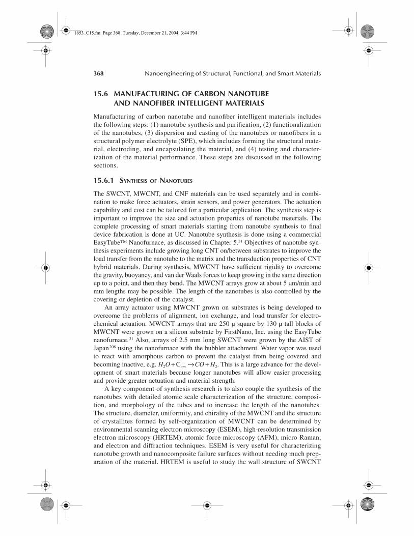
368 Nanoengineering of Structural, Functional, and Smart Materials
15.6 MANUFACTURING OF CARBON NANOTUBE AND NANOFIBER INTELLIGENT MATERIALS
Manufacturing of carbon nanotube and nanofiber intelligent materials includesthe following steps: (1) nanotube synthesis and purification, (2) functionalizationof the nanotubes, (3) dispersion and casting of the nanotubes or nanofibers in astructural polymer electrolyte (SPE), which includes forming the structural mate-rial, electroding, and encapsulating the material, and (4) testing and character-ization of the material performance. These steps are discussed in the followingsections.
15.6.1 SYNTHESIS OF NANOTUBES
The SWCNT, MWCNT, and CNF materials can be used separately and in combi-nation to make force actuators, strain sensors, and power generators. The actuationcapability and cost can be tailored for a particular application. The synthesis step isimportant to improve the size and actuation properties of nanotube materials. Thecomplete processing of smart materials starting from nanotube synthesis to finaldevice fabrication is done at UC. Nanotube synthesis is done using a commercialEasyTube™ Nanofurnace, as discussed in Chapter 5.31 Objectives of nanotube syn-thesis experiments include growing long CNT on/between substrates to improve theload transfer from the nanotube to the matrix and the transduction properties of CNThybrid materials. During synthesis, MWCNT have sufficient rigidity to overcomethe gravity, buoyancy, and van der Waals forces to keep growing in the same directionup to a point, and then they bend. The MWCNT arrays grow at about 5 µm/min andmm lengths may be possible. The length of the nanotubes is also controlled by thecovering or depletion of the catalyst.
An array actuator using MWCNT grown on substrates is being developed toovercome the problems of alignment, ion exchange, and load transfer for electro-chemical actuation. MWCNT arrays that are 250 µ square by 130 µ tall blocks ofMWCNT were grown on a silicon substrate by FirstNano, Inc. using the EasyTubenanofurnace.31 Also, arrays of 2.5 mm long SWCNT were grown by the AIST ofJapan208 using the nanofurnace with the bubbler attachment. Water vapor was usedto react with amorphous carbon to prevent the catalyst from being covered andbecoming inactive, e.g. H2O + Cam →CO + H2. This is a large advance for the devel-opment of smart materials because longer nanotubes will allow easier processingand provide greater actuation and material strength.
A key component of synthesis research is to also couple the synthesis of thenanotubes with detailed atomic scale characterization of the structure, composi-tion, and morphology of the tubes and to increase the length of the nanotubes.The structure, diameter, uniformity, and chirality of the MWCNT and the structureof crystallites formed by self-organization of MWCNT can be determined byenvironmental scanning electron microscopy (ESEM), high-resolution transmissionelectron microscopy (HRTEM), atomic force microscopy (AFM), micro-Raman,and electron and diffraction techniques. ESEM is very useful for characterizingnanotube growth and nanocomposite failure surfaces without needing much prep-aration of the material. HRTEM is useful to study the wall structure of SWCNT
1653_C15.fm Page 368 Tuesday, December 21, 2004 3:44 PM

Nanoscale Intelligent Materials and Structures 369
and MWCNT. Raman is used to determine the nanotube diameter. The diameteris related to the (m, n) indices, and the chirality of SWCNT can be determinedby knowing the diameter based on the Raman results.
15.6.2 FUNCTIONALIZATION OF NANOTUBES
Purification and functionalization are essential in defining active surface area,charge transfer rate, and adsorption/desorption at the CNT surface. Creating astrong bond (interface) between the nanotubes themselves and between nano-tubes and the matrix materials in the case of composite materials is crucial fordesign of sensors and actuators. The UC has developed a plasma polymerizationprocess to coat or functionalize CNT with different materials.159–164 In a plasmagas environment, the surface atoms of the CNT become activated. At these activecenters, a polymer film will form on the CNT surface. The polymerizationconditions can be controlled so that the structure of the coating film has thedesired number of functional groups. The plasma coating process is well describedin Chapter 8.
Functionalization research related to smart materials is focusing on increasingthe electrochemical ion exchange at the nanotube surface when the nanotubes arecast into a solid polymer electrolyte (SPE). The individual nanotubes are coatedwith an ultra-thin coating of acrylic acid or polypyrrole using plasma polymerizationbefore dispersing and mixing in the polymer electrolyte using simultaneous sonica-tion and shear mixing. The different functionalization methods can be tailored tochange the mechanical, electrical, and magnetic properties of the CNT due to acombination of dimensional changes and interface properties. In combination withplasma coating, surfactants used with ultra-sonication have been found to be a goodapproach to disperse nanotubes. Using 1% by weight of random SWCNT or nano-fibers, and the UC functionalization and dispersion methods, 30 wt% to 40 wt%increase in elastic modulus of epoxy has been achieved. Up to 15% by weight ofnanotubes have been incorporated in epoxy, but the dispersion techniques for thislarge loading are still being developed. Nafion has also been used to coat CNT tomake electrochemical actuators. The experience in reinforcing composites is usefulto develop CNT actuators. The challenge is to improve the speed of the ion exchangeand increase the strain transfer of the nanotube actuator in the SPE. Sometimes thenanotubes may be filled with the SPE. A nanotube filled with the SPE is called acomposite nanotube, because the nanotube is the host material, while integratingnanotubes in the SPE produces a nanotube composite, because the SPE matrix isthe host material.
15.6.3 CASTING NANOTUBES AND NANOFIBERS IN A STRUCTURAL POLYMER ELECTROLYTE
There are particular challenges that must be met before nanotube propertiescan be fully exploited. The main problem is to attain good dispersion andinterface bonding between the CNT and the polymer matrix and achieve goodload transfer from the matrix to the CNT during loading, since colloidal mate-rials such as CNT do not spontaneously suspend in polymers.192–199 Dispersion
1653_C15.fm Page 369 Tuesday, December 21, 2004 3:44 PM

370 Nanoengineering of Structural, Functional, and Smart Materials
may be the most critical part of integrating any of the types of nanotubes intopolymers or other host materials. Sonication is often used to disperse nanotubesin solvent or resins. Too low of a sonication power level will not satisfactorilydisperse the nanotubes. On the other hand, too high of power level will breakthe nanotubes apart and shorten the nanotubes. During sonication, resonantbubbles are formed and collapse, generating very high local pressures andtemperatures. Different sizes of nanotubes require different levels of sonicationto achieve dispersion without shortening the nanotubes. To resolve these issues,many groups are trying to disperse CNT homogeneously and uniformly inmatrix materials. Solvents including amides, NN-dimethylformamide (DMF),and N-methylpyrrolidone (NMP) were reported to provide solubility of CNTfor different applications. Using appropriate surfactants, CNT can also besolubilized in water. 90 Also, SWCNT have been solubilized by functionalizingthe end-caps with long aliphatic amines or the sidewalls with fluorine andalkanes. By using an ultra sound mixer or using strong acids, good CNTdispersion can be achieved 68 for lower percentages of nanotubes from about 1wt% to 3 wt% of SWCNT. Dispersing larger percentages of nanotubes inpolymers remains a problem. Recently NaDDBS has been reported to be anexcellent surfactant for dispersing nanotubes in water. 90 A filtering and dryingprocedure is needed to prepare the surfactant dispersed nanotubes for incorpo-ration into epoxy and PMMA polymers. High shear mixing is also critical toseparate nanotubes.
For the smart structures applications requiring the high conductivity of CNT,coating of metals and organic conductive polymers (CP) on the surface of CNT toproduce CNT-reinforced composites is another method.192–199 CNT coated withpolypyrrole, Ni, Co, Ti, W, Pd, Au, Al, and Fe to form composites are not uniformand homogeneous, resulting in tangling and random distributions.125 CP such aspolypyrrole, polyaniline, and polythiothene can be used as the conducting matrix,but these are mechanically weak and have to be oxidized and doped by a counteranion to achieve significant conductivity.126,128,129 With large enough percentages ofCNT in the insulating matrix, the nanotube-reinforced composite may be an ionicallyconductive structure that has satisfactory mechanical strength. Careful considerationto choosing the appropriate solid polymer matrix and coating materials is a key issuein synthesizing smart materials using nanotubes. Loading polymers with nanotubescan be done using SWCNT, MWCNT, or CNF. SWCNT that have a perfect atomicstructure are electrically the best filler, but the cost is high and the chiralities cannotbe easily separated. MWCNT do not have good shear stress transfer between theindividual shells, and the number of walls usually increases the number of defects.It appears that the inner layers provide mechanical support, unless electrical contactis made with the inner layers. CNF have lower electrochemical properties thanMWCNT. At UC, the ultra sonication and shear mixing steps are combined in theprocedure for the dispersion of nanotubes in epoxy. This shortens the time of samplepreparation. The combined setup is shown in Fig. 15.2. A procedure for processingsmart nanocomposite materials is being developed that includes (1) nanotube synthe-sis, (2) plasma polymerization or acid oxidization functionalization, (3) dispersion ina solvent annealing, and then dispersing in the resin, (4) casting using high-pressure
1653_C15.fm Page 370 Tuesday, December 21, 2004 3:44 PM

Nanoscale Intelligent Materials and Structures 371
consolidation or vacuum degassing, (5) curing, and (6) cutting, electroding, andencapsulating the smart material.
Precise control and optimization of all processing steps is extremely importantto fabricate nanostructured smart materials. Therefore we are developing a vacuumprocessing system for the fabrication of CNT smart materials. The vacuum pro-cessing system shown in Fig. 15.2 allows sonication and mechanical mixing ofthe nanotubes and SPE at elevated temperature in a partial vacuum or inert gas.High-pressure consolidation of the liquid nanocomposite material to fill the largeropen nanotubes with the resin is also being done. This fabrication procedure alongwith using longer nanotubes is expected to significantly improve the performanceof nanocomposite materials. The actuation and strength properties of the nano-composites produced are determined using electrochemical impedance spectros-copy, load and displacement testing, mechanical strength testing, and microscopy.The following section discusses recent research and presents ideas to developnanotube sensors and actuators for smart structures and nanotube-based healthmonitoring systems.45,66–68,200–202
15.6.4 CARBON NANOTUBE COMPOSITE STRAIN SENSORS
Carbon nanotube piezoresistive sensors are being considered for self-monitoringof composite structures. The CNT and CNT-epoxy have a number of differentsensing properties. There has been investigation of these properties and whatproperties are optimal for different applications. Figure 15.3(a) shows a ∼2-mmthick CNT-epoxy sensor with 5% randomly oriented CNT. The piezoresistive effect(resistance change with pressure) is also shown. The contact resistance35–43 of theCNT-epoxy/metal contacts causes the large slope in Fig. 15.3(a). Silver-filledepoxy can eliminate most of the high-contact resistance. Resistance that decreaseswith compressive loading may also be due to pushing the CNT closer togetherimproving hopping/tunneling and direct contact in the epoxy matrix. The electros-trictive effect (quadratic charge due to strain) of the matrix material is shown in
FIGURE 15.2 Simultaneous ultrasonication and shear mixing (a) of a nanotube polymer ina glove box (b).
Humidity, temperature,pressure and
atmospheric control
Ultrasonicatortip and rotary
mixer
(a) (b)
1653_C15.fm Page 371 Tuesday, December 21, 2004 3:44 PM
372 Nanoengineering of Structural, Functional, and Smart Materials
Fig. 15.3(b). A 0.5-volt peak signal is produced due to an impact; Fig. 15.3(c)shows a 100% CNT film sensor, R = 12 ohms; Fig. 15.3(d) shows a pressure-castCNT-epoxy barrel sensor, R = 400 ohms; Fig. 15.3(e) shows a CNT-epoxy sensorplate with electrodes on top and bottom. These are early examples of self-sensingstructural materials.
Since macroscale strain sensors are needed, the nanotube resistance propertiesmust be brought to the microscale. Different nanotube systems including individualSWCNT, MWCNT, CNF and ropes and mats can be used for making piezoresistivesensors. It may also be possible to build nanotube switches sensitive to very smallpressure changes. A carbon nanotube neuron crack sensor for SHM is shown inFig. 15.4. The crack sensor can be a highly reliable safe-life sensor that will ensure thatno crack length larger than the spacing between two parallel carbon nanotubesensor nerves exists. Modeling and different polymers are being used to improvethe sensitivity. NASA Langley researchers200 are also developing a carbon nano-tube strain sensor. Rice University researchers177 have developed a buckypaperpiezoresistive sensor.
FIGURE 15.3 SWCNT sensors built at UC: (a) 5% CNT load sensor and resistance versuscompressive load, (b) voltage (0.5 v peak) versus time due to impact on an electrostrictivepolymer, (c) 100% SWCNT film sensor, R = 12 Ohms, (d) pressure-cast CNT-epoxy barrelsensor, R = 400 Ohms, (e) CNT-epoxy sensor plate with electrodes on top.
0
20
40
60
80
100
0 50 100 150 200
Load (N)
Res
ista
nce
(K-O
hm) (a)
(d)
(e)
(c)(b)
−2 2−1.5 1.5 2.5× 10⁻¹
−0.5
−0.5
−0.4
−0.3
−0.2
−0.1
0
0.1
0.2
0.3
0.4
0.50−1 1
Time (sec)
Vol
tage
Impact response of CNT/epoxy
1653_C15.fm Page 372 Tuesday, December 21, 2004 3:44 PM

Nanoscale Intelligent Materials and Structures 373
15.6.5 A CARBON NANOTUBE–BASED BIOSENSOR
Biomedical applications of nanoscale intelligent materials have an especially largepotential. Three applications can be categorized as (1) biomedical diagnostic tech-niques, (2) drugs, and (3) prostheses and implants. Biomedical applications for useoutside of the body, including diagnostic sensors such as DNA, RNA chips, Lab-on-a-chip, and micro-total analysis systems (µTAS) are suitable for analyzing bio-molecular samples. For inside the body, several researchers are developing anticancerdrugs, bio-MEMS devices, and gene therapy. Other researchers are working onprostheses and implants that include nanostructured materials.
Current biological sensors commonly rely on optical detection principles thatare inherently complex, requiring multiple steps, multiple reagents, preparativesteps, signal amplification, and a relatively large sample size. Therefore, thesetechniques are highly sensitive and specific, but difficult to miniaturize. In order toovercome these limitations, a carbon nanotube array–based sensor is consideredusing the electrochemical properties of nanotubes for biosensors. Based on thisidea, different possible uses of nanotubes for sensors are studied. Sensors caninclude strain sensors, electrochemical biosensors, gas chemical sensors, tempera-ture, and light sensors. A limiting factor for developing artificial organs such aseyes or ears is the interface between the biological component and an artificialsilicon chip. A remarkable solution for this problem is a CNT array that can directlycontact a cell in vivo, since CNT provide a highly biocompatible surface. One ofexample is a vision chip consisting of an array of electrically conductive CNTtowers grown directly on the surface of a silicon chip. A group has already testedthe implant materials with retinal ganglion cells in vitro and proved the excellentbiocompatibility.201
FIGURE 15.4 A MWCNT/PMMA 10% wt. neuron continuous strain sensor fabricated usinga spray-on technique; (a) a (300 mm × 5 mm) neuron on a composite beam; and (b) dynamicresponse of the neuron on the vibrating beam.
(a)
(b)
MWNT/PMMA neuron (yellow)
Laser sensor (red)
1653_C15.fm Page 373 Tuesday, December 21, 2004 3:44 PM

374 Nanoengineering of Structural, Functional, and Smart Materials
The nanotube-based electrochemical sensor can reduce the drawbacks of otherelectrode materials that include short life, low conductivity, and low reliability. Forbiosensing applications, carbon nanotubes have advantages of small size, a largesurface area, high sensitivity, fast response, and good reversibility at room tem-perature. At the same time, carbon nanotube biosensors can be integrated withmicroelectronics and microfluids systems to gain advantages in miniaturization,multiplexing, and automation. Carbon nanotubes functionalized with special chem-ical groups can form an electrochemical biosensor for enzyme immobilization andstabilizers and mediators used in cancer research. The UC is focusing on thedevelopment of a carbon nanotube array–based cancer sensor. The nanotube arraybecomes a miniature bioelectronic sensor with a large number of functionalizedantibody sites for high sensitivity. The design of the nanotube array determines thesensitivity of the sensor. The research is to synthesize MWCNT in an interdigitatedpattern, as shown in Fig. 15.5. Based on this array pattern design, the fabricationand processing can be done using semiconductor processing techniques. The com-plex CNT array pattern is expected to improve the detectability and fast responseof the sensor and provide reliable data with minimal false positive and false negativereadings. This array could also be put on a chip in a portable device to create a lab-on-a-chip system with a microflow channel.
The semiconductor processing steps to form the array are shown in Fig. 15.6.These steps are preliminary and are under early development and can be used to growlarge planar arrays of MWCNT that can be sectioned to provide many sensor elements.The critical step to develop the CNT array–based sensor is the fabrication process.Figure 15.6 illustrates the proposed detailed sequential steps in the fabrication processof the sensor segment. The starting substrate in Step 1 is either a highly resistive Sisingle crystal wafer or sapphire. This provides an insulating base, which is requiredfor the wiring of the segment. Step 2 involves deposition of highly conductive (doped)poly Si for planting the CNT catalyst on it. Doped Si provides good electrical contactbetween the CNT and the substrate. The CVD technique is used for depositing polySi doped either with P or As. As an alternative solution, one can use an insulating Siwafer that is ion-implanted on the CNT growth side for increasing the electricalconductivity. Steps 3 to 7 involve patterning and require sputtering of a thin metal film(20–40 nm) of catalyst such as Co and thermal annealing of the film in hydrogen at825°C. During the annealing, catalytic semispheres of Co islands are formed driven
FIGURE 15.5 Concept nanotube interdigitated array biosensor.
Vertical doublerow MWCNTSfunctionalizedwith antibodies
+ electrode
− electrode
1653_C15.fm Page 374 Tuesday, December 21, 2004 3:44 PM

Nanoscale Intelligent Materials and Structures 375
by surface tension to lower the total energy. Simultaneously a chemical reactionbetween the metal and the Si substrate takes place, producing highly conductiveCoSix. This compound is expected to provide a strong mechanical bond betweenthe CNT and the substrate and also serve as a low resistivity electrical junction.The patterned substrate with catalyst provides aligned growth of MWCNT duringStep 8. Functionalization of the array by solution methods or plasma coating isshown in Step 9. The patterning and functionalization will be optimized to matchthe specific antibodies to be immobilized and the growth factors and cytokine tobe sensed. Medical doctors at UC are involved in the design. Immobilization ofthe antibodies is shown in Step 10. In this design, the electrical signal can beprovided to each individual column of aligned carbon nanotubes or in almost anyarrangement desired to tune the sensitivity.
The nanotube sensor array can be patterned to have a desired connectivity ofthe individual pairs of nanotube sensors shown in Step 10 of Fig. 15.6. The highestsensitivity of the array can be examined by modeling the impedance of the wholearray when the antibody-growth factor coupling occurs. The nanotube spacing inthe array, and the nanotube diameter, length, and functionalization must be optimizedto give the greatest sensitivity while rejecting small changes in sensitivity that couldlead to false positive and false negative indications. The functionalization improvesthe electrochemical response of the array to specific proteins, enzymes, and growthfactors on the surface of CNT. At UC, various chemical groups such as -COOH andNH2 are coated on the nanotubes to optimize the electrochemical response from theCNT array–based electrode acting as a host for different biospecies. The function-alization can be done in two ways for comparison. One is a reagent bath in whichacids are used to attach specific function groups to the nanotubes. This method is
FIGURE 15.6 Fabrication steps for the double-row interdigitated nanotube array sensor ofFig. 15.5.
Highresistivity Si
Doped poly Si
Photoresist
UV
Shadow mask
Co or Ni
Co or Ni
Sputtering of Co
Etching
Coat with photoresist
Deposition of doped poly Si
Step 1 Step 7
Step 8
Step 9
Step 10
Step 2
Step 3
Step 4
Step 5
Step 6
Thermal treatmentat 825°C in Ho
CoCoSix
CNT
CNT
CNT growth
Functionalization
Immobilization
Antibodies
1653_C15.fm Page 375 Tuesday, December 21, 2004 3:44 PM

376 Nanoengineering of Structural, Functional, and Smart Materials
the current conventional method that is widely used to functionalize nanotubes.Plasma surface modification is the other very promising method for nanotube func-tionalization. In the plasma technique, for example, water and oxygen may be usedto functionalize the surface of the MWCNT array instead of using a monomer suchas styrene or pyrrole that is used for polymer coating. In the plasma phase, thecarbon atoms on the surface are active and react with water or oxygen molecules toform -COOH and -OH groups. If -NH2 is needed, ammonium hydroxide and NH3
gas can be used as the monomer as well.The carboxyl function groups that are functionalized on the nanotube surface will
react with biospecies such as enzymes, antibodies, and oligonucleotides and formstrong covalent bonds to attach biospecies to the surface of the nanotube. Dependingon the different biospecies attached on the surface, the aligned CNT can be used todetect DNA, hydrogen peroxide, glucose, and other biomolecules. As an example, acarboxyl function group was attached to the MWCNT by surface modification. Anamino function group on the oligonucleotide probe can react with the carboxyl functiongroup to form covalent bonds and attach the probe on the surface of the nanotube.When this kind of biosensor is put into the test solution, the species in solution canattach on the probe. When immobilization occurs, a different electrochemical responseoccurs; the change in the impedance spectra or current is used to detect the presenceand the amount of the complementary sequence. Figure 15.7 shows the experimentalsetup for the electrochemical bionanosensor for on-site analysis. The electrochemicalsystem is based on amperometric or electrochemical impedance measurements.
Once the nanotubes are functionalized using the plasma system, immobilizationof antibodies on the nanotubes must be done. Antibody immobilization formats canbe broadly categorized into two classes: direct labeling experiments and dual antibodysandwich assays. These methods are possible for use with the nanotubes. However,based on our experience functionalizing carbon nanotubes, the carboxyl function groupis very active and it can react with the -NH2 function group via carbodiimide activation.A possible approach is to use the plasma coating method to functionalize the nanotubesbased on our existing technique and use solution methods to immobilize the antibodiesand use techniques such as FTIR, and TOFSIMS to characterize the immobilization.
FIGURE 15.7 Electrochemical analysis setup using; (a) a Gamry potentiostat, and (b) func-tionalized MWCNT (ESEM image by Srinivas Subramaniam, Univ. of Cincinnati MaterialsCharacterization Center).
CNF-GOxelectrode
Buffer sol.
SCE
Counter
Working
PotentiostatPCI board
Magnetic stirrer
1653_C15.fm Page 376 Tuesday, December 21, 2004 3:44 PM

Nanoscale Intelligent Materials and Structures 377
The amperometric method, especially cyclic voltammetry, is carried out since it canmeasure the concentrate-dependent current through the CNT array–based electrodecoated with a specific chemical group. Each human has on the order of 50,000 genesthat might play a critical health-related role. Biosensors that can perform genetic analy-sis, therefore, have tremendous potential. At the UC, initial experiments to develop ananotube biosensor were performed.
Figure 15.8 shows the Electrochemical Impedance Spectroscopy (EIS) data(Nyquist plot) with imaginary (Capacitive) vs real (Resistive) components of thecomplex impedance. Three different potentials were tested; 0.2 V, 0.4 V, and 0.6 V.Figure 15.8(a) shows the EIS results before the immobilization of GOx on the surfaceof the CNF film and Figure 15.8(b) shows the EIS results after Gox is immobilized onthe surface of the CNF electrode. With the immobilization of the Gox on the nanotubes,the impedance of the sensor changes as shown by comparison of the responses (a)to (c) in Figure 15.8(a) and Figure 15.8(b). The change in impedance is due to thechange in the electrical resistance and capacitance of the electrode due to theimmobilization of the Gox. This result indicates the potential to use the bioelectronicsensor for label-free sensing. Figure 15.8(c) shows the amperometric response ofthe biosensor in which 1 mM glucose is added at each step at a potential of 0.5 Vin PBS (pH 7). Even though there is slight noise in the signal caused by the 1 µAresolution level of the Gamry system, the current response increases immediatelyafter each addition of 1 mM of glucose in the PBS solution. This change in responseis repeated five times and keeps the same value for 200 seconds. This high sensitivityand stability are an advantage of CNF-Gox biosensor for commercial applications.The structure of the CNF provides a large surface area to immobilize the Gox andmaintain this high activity. At the same time, CNF could promote the electron transferin the bioelectrochemical reaction.
A biosensor architecture based on carbon nanotubes may detect cancer and otherpathogens at the earliest stages using electrochemical sensing of molecular signatures
FIGURE 15.8 Biosensor characterization using glucose: (a) Electrochemical impedancespectra for the biosensor at DC potentials 0.2 V (a), 0.4 V (b), and 0.6 V (c) before immo-bilization of GOx; (b) after immobilization of GOx on the CNF; (c) The amperometric responseat an applied potential of 5 V versus the SCE reference electrode from the CNF-based sensordue to the successive addition of 1 mM glucose in a 0.05 M phosphate buffer solution (pH 7).
2000
1500
1000
00
500Zim
ag (
Ohm
)
Zreal (Ohm)500 1000 1500 2000
(a)
(b)(c)
2000
1500
1000
00
500Zim
ag (
Ohm
)
Zreal (Ohm)500 1000 1500 2000
(a)
(b)
(c)
3
3.5
2.5
2
1.5
1
×10−6
0 200 400 600 800
Cur
rent
(A
)
Time (sec)
(a) (b) (c)
Increasingfreq.
1653_C15.fm Page 377 Tuesday, December 21, 2004 3:44 PM

378 Nanoengineering of Structural, Functional, and Smart Materials
that can identify diseases. The nanotubes are good biosensors because their smallsize can allow detection of small numbers of biomolecules and the nanotube resis-tance and capacitance one sensitive to the attachment of biomolecules on the wallsof the nanotube. The smaller size and higher sensitivity of the sensor may provideearly detection and better outcomes for many diseases including cancer. Theapproach using interdigitated array architecture and a plasma coating method isexpected to improve sensitivity and speed of detection as compared to existing typesof sensors, and as compared to using a multiplexing approach with statistical analysisof separated individual arrays.
15.6.6 CARBON NANOTUBE AND NANOFIBER HYBRID ACTUATORS
In order to develop actuators for practical structural applications, there are manychallenges. Therefore at the UC we have been developing a polymer host fornanotubes that can provide ion exchange for the electrochemical effect.192–199 Verylittle or no previous research has been done using CNF for electrochemical actuation.Even though the electrochemical properties of CNF are smaller, we are focusing onCNF for new actuators because the cost is low at $0.25/gm (∼$100/lb), and incor-poration of the nanofibers into polymers is easier because the fibers are large(∼70–150 nm). The CNF material is also readily available in commercial quantitiesand large components that can be made. The Bionanotechnology Lab at UC isdeveloping for the first time a carbon nanofiber (CNF)–polymethylmethacrylate(PMMA) composite material that has electrochemical actuation properties. A com-bination of solvent casting and melt mixing was used to disperse CNF in PMMAand cast thin films of the material. Solution casting of the actuator material is shownin Fig. 15.9(a) for use as a wet actuator. Since PMMA/CNF composites have electri-cal resistance, to develop the actuator, sputtering of metal particles on the surfaceof PMMA/CNF composite is one approach being investigated to provide a uniformvoltage field.
FIGURE 15.9 Manufacturing steps for the CNF-PMMA hybrid actuator: (a) CNF in a poly-mer matrix, (b) actuator strips as produced and with sputtered gold electrodes, (c) SEM imageof fracture surface with fiber pullout. (SEM image by Robert Gilliland.)
Nanocomposite
NanofiberPolymer
+
CNT/PMMAcomposite Insulated
layer Gold
(a) (b) (c)
1653_C15.fm Page 378 Tuesday, December 21, 2004 3:44 PM

Nanoscale Intelligent Materials and Structures 379
The electrodes of the actuator should be insulated from the electrolyte becausewe have found that only the top part of the actuator provides most of the actuation.This is due to shunting through the electrolyte and a nonuniform voltage along theactuator. Tailoring of the voltage along the actuator and encapsulation of a partiallyhydrated actuator are approaches that are under investigation to overcome thisproblem and to further improve the actuation performance. The CNF-PMMA mate-rial produced using the solution casting procedure is shown in Fig. 15.9(b). Theactuators shown are from 1 inch to 6 inches in length. Larger actuators and compo-nents can be made because the CNF and chemicals are low cost. In Fig. 15.9(c), thefailure surface is shown in which the nanofibers are shown pulling out of the matrixmaterial. The interfacial bonding of the CNF to the polymer is currently weak andwill be improved using the plasma coating and dispersion methods.
Solution casting of the CNF-PMMA actuator for use in wet electrolytes is shownin Fig. 15.10(a). Figure 15.10(b) shows the experimental setup for the CNF-PMMAactuator. These aqueous-based actuators are immersed in a 2 M NaCl solution. Square
FIGURE 15.10 Solution casting and testing of the wet CNF-PMMA hybrid actuator:(a) solution casting, (b) typical experimental setup, (c) actuator response, (d) measuredresponse near fixed end (out of water) of actuator.
(c) (d)
(a)
4 6 8 10 12 14
0
2
4
6
8
−0.9
−0.8
−0.7
−0.6
−0.5Displacement & applied voltage
Time (sec)
Low voltage (8 V)High voltage (20 V)
CNT/PMMAsolution
CNT/PMMAsolution
Polymer asinsulator
Laser displacementsensor
Vision sys.
Op. amp &NI board
PotentiostatPCI board
Counter
SCE
Working
Electrolyte
CNT actuator
Drying
Drying
(b)
Dis
plac
emen
t (m
m)
App
lied
volta
ge (
V)
1653_C15.fm Page 379 Tuesday, December 21, 2004 3:44 PM

380 Nanoengineering of Structural, Functional, and Smart Materials
wave potentials are applied between the platinum counter electrode and the workingelectrode. The displacement of CNF-PMMA actuator is shown in Fig. 15.10(c) and ismeasured by a laser displacement sensor (Keyence, LC-2400 Series) and monitoredusing a vision system (Intel Pro PC Camera). Note the very large actuation at 20 volts.This is due to surface actuation because of poor dispersion of the CNF. Also notice thatthe bending occurs mostly near the top of the actuator. This is because of shunting inthe electrolyte and because the resistance of the actuator reduces the voltage in thelower part of the actuator. Improved dispersion, processing, an insulated electrode, andarray methods will greatly improve the stiffness and bandwidth of the actuator. This isa very exciting material because of the low cost and good actuation.
A square wave with amplitude of +8 V was applied at frequencies ranging from0.2 Hz to 10 Hz. The response was measured near the fixed end of the actuator outof the water at 0.5 Hz and is shown in Fig. 15.10(d). The characterization of theactuators is being done using a specially built test system for electrochemical actu-ators. This PC-based system can be built using readily available components for atotal cost of about $30,000. The displacement of the actuators is measured using alaser displacement sensor (Keyence, LC-2400 Series). Square wave potentials areapplied between two electrodes using a National Instruments PCI board and anoperational amplifier that was designed and built to drive electrochemical actuators.The square wave excitation is an effective way to drive the amplifier and actuatorwith various amplitudes and frequencies using the PCI D/A board. In order to supplyenough power to drive the actuator, a voltage follower and noninverting amplificationwere designed using the OPA2544 (TI) with a gain of 20:1.
Solution casting of a dry actuator material is similar to that for the wet actuator,Fig. 15.11(a). However in the dry actuator procedure the SPE contains the ionexchange material. A dry actuator was constructed according to Fig. 15.11(a) usingindividual CNF cast in a PMMA+LiBF4 SPE. A loading of ∼10% CNF is used inthe actuator in this example. The actuator is formed using two CNF actuators, oneon each side of tape. One actuator is used as ground and the other is switchedbetween +2 and −2 volts. The test setup is shown in Fig. 15.11(b), and the actuationis shown in Fig. 15.11(c). Because the actuator is not hydrated, the actuation is slowand the amplitude is small compared to the wet actuator. Some creep also occurspartly because the actuator is very flexible and the two actuators are not exactly thesame size. Individually coating the CNF, uniformly dispersing the CNF, pressurecasting, and aligning the CNF will improve the actuation. Allowing the material toabsorb a small amount of moisture would also improve actuation. There is an unusualcharacteristic of this actuator. Note in the time response of the actuator shown inFig. 15.11(d) that each time the voltage switches, the actuator returns to equilibriumquickly and then more slowly begins to actuate in the opposite direction. This is theinterplay between the elasticity and ion exchange in the solid polymer electrolyte.
A summary of the main properties of carbon nanotube and carbon nanofiberhybrid actuators is given in Table 15.4. This is the first time some of these materialshave been characterized, and much more detailed characterization is planned.
We are developing the electrical equations of a CNT actuator in an electrolyte.A 2-M NaCl electrolyte solution is used for the experiments. Details of the modelingare given in References 66–68. Electrochemical impedance spectroscopy (EIS) was
1653_C15.fm Page 380 Tuesday, December 21, 2004 3:44 PM

Nanoscale Intelligent Materials and Structures 381
performed on three-electrode cells, with a dry CNF actuator as the working electrode,a saturated Calomel reference electrode (Gamry, Part No. 930-03), and using plat-inum as the counter electrode. EIS measurements were performed using GamryPotentiostat (Model: PCI4/750) coupled with the EIS software (Gamry, EIS300).The cell was equilibrated for several hours after each step. The electrochemicalimpedance spectroscopy (EIS) results are shown in Fig. 15.12.
The EIS results and modeling using Randle’s circuit are discussed in References67, 68. Randle’s circuit is an equivalent circuit representing each component at theelectrode/electrolyte interface and in the solution during an electrochemical raction.The electrode kinetics model the change from electronic conductivity to ionic con-ductivity, in the simplest way, in parallel as a double-layer capacitor and a polarizationresistance that models the electrode kinetics, and this parallel capacitor and resistorcombination is in series with a resistor that models the electrolyte solution resistance.
The CNT actuator must now be modeled as it charges and discharges under anAC environment wherein the actuation is proportional to the basic charge transferrate. Although the electrolysis mechanism with an AC voltage input has very complexcharacteristics, we can model this effect as an impedance element. The relationship
FIGURE 15.11 Solution casting and testing of the dry CNF-PMMA hybrid actuator:(a) solution casting, (b) test setup, (c) dry actuator with two-sided actuation, and (d) measuredresponse due to 0.5 hz ± 4v excitation.
1.6
1.65
1.7
1.75
1.8
Dis
plac
emen
t (m
m)
CNT/PMMAsolution
CNT/PMMAsolution
Drying
Drying
PMMA/LiBF4 solution
CNFactuator
Visionsys.
Laserdisplacement
sensor
Operationalamp.
Niboard
(a)
(c) (d)
(b)
20 2515 30
−4
−2
0
2
4A
pply
ing
volta
ge (
V)
Time (sec)
1653_C15.fm Page 381 Tuesday, December 21, 2004 3:44 PM

382 Nanoengineering of Structural, Functional, and Smart Materials
TABLE 15.4Properties of Carbon Nanotube and Carbon Nanofiber Hybrid Actuators
Type of Actuator Wet Environment (NaCl Solution) Dry Environment (with an SPE)
SWCNT buckypaper Fast, large strain, expensive, good cohesion property to make bucky paper, low strength
Slower response and smaller actuation than wet
MWCNT buckypaper Good actuation strain and lower cost than SWCNT
Slower response and smaller actuation than wet
CNF buckypaper Low cost, difficult to make bucky paper, low mechanical strength, needs higher voltage and current to actuate
Slower response and requires larger voltage, good mechanical loading with the SPE
CNF coated with polypyrrole to form bucky paper
Improved mechanical loading, similar actuation properties as CNF bucky paper
Slower response and requires larger voltage, good mechanical loading with the SPE
SWCNT composite made with PMMA polymer
Fast, large strain, best among nanotube composites, expensive
TBD
MWCNT composite made with Epoxy polymer
Good strength and actuations need to larn make
TBD
CNF composite made with Epoxy polymer
Need higher voltage and current, good mechanical properties, dispersion needs to be improved, has smart structures applications
TBD
FIGURE 15.12 The EIS responses at cell potentials of 0.1 to 0.4 V; (a) 0.05 Hz to 100 KHz.,and (b) enlarged view of high frequencies between 100Hz-100KHz.
Increasingfrequency
3000
2000
1000
00 2000 4000 6000 8000
0.2 V
0.3 V
0.4 V
Zim
ag (O
hm)
Zreal (Ohm) Zreal (Ohm)
(a)
0.1 V
Zim
ag (
Ohm
)
150
100
50
0100 150 200 250
0.2 V
0.3 V
0.4 V
0.1 V
(b)
1653_C15.fm Page 382 Tuesday, December 21, 2004 3:44 PM

Nanoscale Intelligent Materials and Structures 383
between mechanical properties and electrical properties can be expressed approxi-mately by the linear relation:
(15.1)
Here, e is the actuator strain, q is the charge per unit volume, s is stress, V is inputvoltage, t is time, a is the strain-to-charge ratio, E is the elastic modulus, the doublelayer capacitance is Cv , and x and y are constants that depend on the constructionof the nanotube smart material and the type of electrolyte used. In this method, theSPE will be designed to increase the capacitance and strain-to-charge ratio, whilemaintaining as high of elastic modulus of the material as possible.
Based on a concept developed at UC, by monitoring the voltage source, a self-sensing actuator can be formed as shown in Fig. 15.13. To implement this practicalself-sensing actuator, an electrical bridge circuit is used to measure strain, as shownin Fig. 15.13(a). The electrolyte and CNT contact act as a resistance, R, the interfacebetween the polymer and the electrolyte is modeled as the double layer capacitance,Cv, and the diffusion element is ZD, as shown in Fig. 15.13(a). The self-sensing actuatorwill be used in the feedback control system shown in Fig. 15.13(b), which shows thecontrol scheme to take advantage of the guaranteed stable collocated output feedbackcontrol. Compared to the best-known ferroelectric, electrostrictive, and magnetostric-tive materials, the very low driving voltage of CNT is a major advantage for developingvarious actuator applications. Other predicted future advantages are the direct conver-sion of electrical to mechanical energy, high actuation strain, strength, and modulus.
The reference model of Fig. 15.13(a) can determine the strain in the actuatordue to the piezoresistive effect of the nanotube composite. We have demonstratedthis effect in which the electrical resistance of the material changes with strain:Tension increases the resistance, and compression decreases the resistance. Thissensing idea can allow the same material to act as an actuator and as a strain sensor.Actually there are three interesting effects acting together in the nanotube actuator:the electrochemical actuation, the piezoresistive effect, and the electrochemical
FIGURE 15.13 Modeling of CNT actuators: (a) UC self-sensing CNT circuit; (b) controllerdesign.
q t
t
x y
C E
V t
tv
( )
( ) /
( )
( )e a s
=
1
Zp Rd
Rd
Reference model
V2
Rs
Rs
Cd
Cd
CNT actuator model
Rp
Rp
V1
V
(b)(a)
OutputInput
Collocated outputfeedback control
Structure withCNT actuators+
−
1653_C15.fm Page 383 Tuesday, December 21, 2004 3:44 PM

384 Nanoengineering of Structural, Functional, and Smart Materials
charge generation effect in which charge is generated by electrolyte flow over thenanotube material without strain. These effects will be studied separately and thena combined model will be produced.
The density of the nanotubes in the SPE has an effect on the electrochemicalactuation. Well-aligned but separated carbon nanotubes produce a large surface areasupercapacitor with high power density. The capacitance of the CNT actuator SPEmaterial is C = Q/V = eo, er(As/t), where Q and V are the charge and voltage,respectively, and eo, er, As, and t are the permittivity of free space, the relativepermittivity, the surface area of the electrode, and the separation the plates, respec-tively. In electrochemical double-layer capacitors (ECDLC) the inter-plate spacingt is reduced to the Helmholz double layer, which is 0.34 nm. The active area of theactuator depends on the density of nanotubes in the composite and the length anddiameter of the nanotubes. A density of at least 50 million CNF/cm2 is expected,and the density of SWCNT will be much greater. The density achievable will dependon how well the nanotubes can be functionalized and dispersed to provide effectiveion exchange and load transfer. The relative permittivity is dependent on the typeof nanotube including the chirality, number of walls, spacing between the walls, anddiameter of the nanotube. There have not been many studies of the electrochemicalproperties of carbon nanotubes in a conductive polymer composite. The transductionproperties of the CNT material must be studied experimentally to determine param-eters to model the strain and to find the optimum material and design to maximizethe capacitance and the ion exchange.
Synthesis of arrays of parallel nanotubes is another approach to make nanotubesmart materials. Embedding planar arrays in layers will allow build-up of compositematerials, as shown in Fig. 15.14(a). Another actuator type can be made by attaching
FIGURE 15.14 Concepts for CNT actuators: (a) SPE hybrid actuator full size; (b) linearactuator shown enlarged (each brick is about 1 mm in height); and (c) tripod actuator shownenlarged (height is about 1 mm), and the rotation is exaggerated for illustration. Multiplelinks connected in series can increase the motion.
A/D converter
Load cell
Controlsignal
Load cell
CNT
Solidelectrolyte
Electrodes
Laserdisplacement
sensorA/D converter
Buildingbrick
figure 1(c)
(b) Linear actuator (c) Tripod actuator(a) Composite actuator
Solid or liquidelectrolyte
CNT actuator
Electrode
1653_C15.fm Page 384 Tuesday, December 21, 2004 3:44 PM

Nanoscale Intelligent Materials and Structures 385
“building bricks” of the array in series by bonding or direct growth in the nanofurnace,as shown in Fig. 15.14(b). A single segment or “building brick” can be used to forma multisegment tilting actuator. A concept for this actuator is shown in Fig. 15.14(c),and the deflection is exaggerated. About 1% strain is expected and the angle ofdeflection will depend on how closely the nanotube “posts” are spaced. The linearor tilting segments may be connected to design active devices from the nanoscaleto the macroscale in size. Inch-size planar arrays can be synthesized and currentefforts are focused on increasing the length of MWCNT. The tilting motion may bebeneficial for alignment and pointing applications. The computer control system willbe used to program the voltage for the actuation.
Based on these experiments, a concept for an electrochemical active catheterhas been devised, as shown in Fig. 15.15. Benjamin Franklin actually inventedthe first catheter. If smart materials could be used to build the active catheterproposed and other miniature manipulators, there would be many medical appli-cations. The catheter has potential for use in angioplasty, stent insertion, plaqueremoval, hydrocephallia, remote surgery, and other applications. Medical deviceinnovation and surgical innovation is a growing area where nanoengineering canmake contributions. In particular methods to increase actuation shope are needed.One concept is telescoping MWCNT’s illustrated in Figure 15.15.
15.7 FUTURE DIRECTIONS FOR INTELLIGENT MATERIALS
This section presents ideas for (near) future applications of nanoscale intelligentmaterials.
15.7.1 A CARBON STRUCTURAL NEURAL SYSTEM
Structural health monitoring (SHM) is a subarea of intelligent structures whereinthe integrity of the structure is monitored in real-time by an in situ sensor system.Several methods of SHM using smart materials have been proposed in the literatureand include damage identification using the vibration response of a structure, fiber-optic strain measurement, stress wave propagation techniques, and wireless MEMS.
FIGURE 15.15 Concept for an active catheter using CNT electrochemical actuation and self-sensing using the principle of electrochemical actuation or telescoping actuation (shown).
Link
Inner tube
CNT actuator
Outer tube
1653_C15.fm Page 385 Tuesday, December 21, 2004 3:44 PM
386 Nanoengineering of Structural, Functional, and Smart Materials
These techniques for in situ real-time SHM may not be cost-effective for applicationto large structures and structures that have complex geometry such as joints, ribs,varying thickness, fasteners, varying curvature, hybrid materials, or materials thatare highly damped such as honeycomb sandwich structures. Although there areseveral types of SHM systems being developed, practical on-board SHM systemsshould add the lowest complexity with the highest benefit. This section describes aconcept for a new sensor system architecture9 that can make practical the use oflarge numbers of miniature sensors to monitor mechanical, civil, and environmentalsystems that can benefit from highly distributed sensors and massively parallelprocessing using a small number of channels of data acquisition. In biologicalsystems, millions of identical parallel nerves are used for sensing. This architectureallows billions of bits of sensory information to be processed in the neural, auditory,and visual systems in an efficient hierarchical order and in harmony. The advantagesof this biological system are recently being duplicated by man. This intersection ofbiological function with nanoscale perfection may lead to an efficient and intelligentstructural neural system (SNS).202
One of many possible architectures for the SNS is in the form of an array oforthogonal intersecting nerves built using carbon nanotubes. This approach isbased on a design in which piezoceramic receptors are used to detect acousticemissions or high strains caused by damage propagation.9,20,25–27 The carbon nan-otube SNS works broadly on the principle of the biological nervous system.27 Thesensor fibers act as a neuron and each neuron is connected to other neurons. Inthe event of high strain or damage to the material, the piezoresistive sensor/neuronchanges resistance and changes the voltage of the neuron. In a biological systemthe signal from one neuron is transmitted by special molecules called neurotrans-mitters that cross the synaptic gap to receptor sites on the target neuron. The signalfrom a biological neuron is inhibitory or excitatory, not both. Excitatory signalstend to fire the target neuron, and inhibitory signals tend to prevent firing. In ourSNS the firing of the neuron depends on the threshold voltage of the sensor. Ifthe voltage is above a certain level, the sensor/neuron sends an excitatory signalthat in turn combines with other firing neurons, and thus the signal is transmitted.Additional layers of hierarchy are possible. If the sensor/neuron is far away fromthe damage event, it will generate a voltage that is below the threshold, so theneuron will not be allowed to fire and it will act as an inhibitory signal tosubsequent neurons. The threshold can be determined by having a capacitor/resistorin the circuit. This is analogous to synaptic transmission of a signal in a biologicalnervous system. The signal from the closest sensor/neuron can be processed toextract the information about the damage. The other neurons can be preventedfrom firing (occluded) to eliminate unwanted signals. The threshold voltage canbe determined by experimentation and simulation depending on the size and typeof SNS. This approach uses receptors that cross but that are electrically indepen-dent. This allows individual row and column neurons to be formed in horizontalrows and vertical columns, as shown in Fig. 15.16. A single neuron is shown inFigure 15.4(a).
A unit cell of the SNS consists of two row receptors and two column receptors.When damage occurs near one receptor, the row and columns of that receptor fire
1653_C15.fm Page 386 Tuesday, December 21, 2004 3:44 PM

Nanoscale Intelligent Materials and Structures 387
and the other rows and columns are inhibited or occluded, depending on the designand training of the neurons. The intersection of the rows and columns that are firingwill show the location of the damage. Also any change in the resistance of theneuron can be related to the strain and damage in the structure. This system isredundant and minimizes false signals. If damage causes one neuron to becomeinoperable, a problem would be indicated by the failed neuron, and the damagewould also be detected when it propagates to the neighboring neuron. Since theneurons can be scaled to the micron or smaller level, an arbitrary degree of sensi-tivity can be obtained.
This SNS can use low-frequency data acquisition, but requires a very high sensordensity to detect initiating damage. For example, crack propagation around rivetsrequires a small-scale unit cell around each rivet. This is practical due to the smallsize and high strain sensitivity of CNT strands. No diagnostic signal or amplifiers orlarge sets of historical data are needed in this simple approach. In addition, the sizeof the carbon SNS can be miniaturized such that the nerves can be put insidecomposite materials or at the bonding interface of joints without affecting the integrityof the structural material. This approach overcomes many of the problems of embed-ding sensors inside composites. The piezoresistive sensors are highly distributed,simple, less expensive, less intrusive, and more sensitive than existing SHM sensortechnology. Figure 15.16(a) shows biological neurons, and Fig. 15.16(b) shows anarray SNS with ten row and ten column neurons (N1-N20), which are continuoussensors that sense along their entire length. The row and column neurons in thearray are routed into four signal channels—two channels of time response signalsand two channels for neuron firing. Using information from these four channels, itis possible to locate the damage source and measure the signal amplitude. The A/Dconversion is only needed at the PC level, and this reduces the complexity of theinstrumentation and the cost, size, and weight of the SHM system. It is anticipatedthat continued development of the array SNS using nanotube-based sensors will leadto ultra-high-density high-sensitivity sensor systems that can be built at either the
FIGURE 15.16 The biological neural system and a concept array carbon structural neuralsystem.
(c) Intelligent aircraft(a) Biological neurons (b) Carbon nanotube array neurons
N1 N10
N11
N20
Channels 1,2Columns output(Neurons 1-10)
Channels 3,4Rows output
(Neurons 11-20)
ProcessorsSquare unit cell
Panelstructure
Continu-ous
sensor
Data acquisition systemand signal processing
On board computerfor damage detection
and warning
Brain
Humannervoussystem
Artificial nervoussystem
Human bodyAdvanced aircraft
1653_C15.fm Page 387 Tuesday, December 21, 2004 3:44 PM

388 Nanoengineering of Structural, Functional, and Smart Materials
macroscopic or the microscopic scale for use on safety-critical structures such asaircraft (Fig. 15.16(c)). The SNS architecture may also have applications in healthmonitoring of living systems and the environment.
15.7.2 HIGH-TEMPERATURE NANOSCALE MATERIALS
Since piezoelectric ceramic materials have been under development for a long time,new materials are sought that can provide increased performance at elevated tem-peratures. There are several nanoscale materials under development that might besuitable for sensing at high temperatures. These materials are in early stages ofdevelopment and are briefly discussed next. References are given where more infor-mation can be obtained.
Nanocomposites with ∼0.5 wt% to 1 wt% of SWCNT can become self-sensingstructures by applying electrodes to the composite surfaces, but a host material thatcan withstand high temperatures is needed. The piezoelectric effect is small inSWCNT, and it does not seem practical for use in sensing. The electrochemicaleffect of the SWCNT is based on double-layer charge injection that causes bondexpansion. A limitation is that the nanotubes must have an ion exchange for thedouble-wall charge injection to work. For high-temperature applications, a moltenelectrolyte might be used as suggested by Baughman et al.53 The SWCNT are formedat temperatures from 700°C to 1000°C. They are expected to operate at temperaturesup to 500°C, beyond which they can burn in an oxygen environment. Use of a moltenelectrolyte would pose problems in some applications.
Noncarbon nanotubes have received much less attention in recent years andremain relatively unexplored. The BNT are predicted to be piezoelectric in bundlesand the maximum piezoelectric-induced stress constant occurs for the specific (5,0)chirality, but the piezoelectric d coefficient is about 20 times smaller than for piezo-ceramics. (See Chapter 21.) BNT materials are the subject of different investigationsstarting in about 2000 and their characteristics offer the possibility of piezoelectricactuation tailored over a wide bandwidth, and the possibility of replacing piezocer-amic materials with BNT. However, the synthesis of BNT is at an early stage (seeChapter 21) and the information on this issue in the scientific literature is limited.There appears to be no experimental verification of the properties of the BNT, andit is not possible to control the chirality of the nanotubes produced. BNT are formedat temperatures above 1000oC. They are expected to operate at temperatures up to1000°C. BNT are one possible material for high temperature applications.
Silicon carbide nanotubes (SiCNT) are under early stages of synthesis at NASAGlenn, as described on the web site.10 Macroscopic SiC is a very hard and heat-resistant ceramic material. The objective of this approach is to take advantage ofthe properties of SiC to synthesize and characterize SiCNT for high-temperatureand high-radiation conditions. Multiple synthetic approaches are being consideredthat parallel the direct CNT formation, as well as an indirect approach involvingderivatization of a CNT to a SiCNT. Recently SiCNT were produced in-house at NASAGRC. A CVD-template synthesis method, in which the template functions as a nano-mold, was employed to produce highly ordered arrays of SiCNT. The arrays arecomposed of individual SiCNT (»200 nanometers in diameter, 60 micrometers in
1653_C15.fm Page 388 Tuesday, December 21, 2004 3:44 PM

Nanoscale Intelligent Materials and Structures 389
length) aligned vertically, with a density of approximately 109 tubes/cm2. The electricaland mechanical properties of the SiCNT are being characterized and compared withtheoretical SiCNT modeling results. Electrical properties studies of nanotubes athigh temperatures could determine the suitability of nanotube high-temperaturesensors. The electrical activity of SiCNT could also be studied as a function ofadsorbates, which could ultimately lead to applications such as nanogas-sensors forharsh environments and sensors for the working area of jet engines.
Bismuth nanowires (see Ch. 3), ZnO nanobelts (see Ch. 4) and other inorganicmaterials such as WS2–MoS2, NbS2, and TiS2 may have piezoelectric or otherinteresting properties that might be useful as sensors.
In summary, existing piezoelectric materials do not have satisfactory propertiesat high temperatures. Some of the different forms of nanotubes that are naturallypolar in bundles or of her fullerene-like may be useful for high-temperature appli-cations. Further research is needed to develop and test the piezoelectric nanotubes.
15.7.3 POWER HARVESTING USING CARBON NANOTUBES
In preliminary experiments we have tested an induced charge generator in anelectrolyte for power harvesting in mechanical and structural systems. The CNTmaterial is shown in Fig. 15.17(a). The voltage due to vertical motion of the filmin the electrolyte was a 7-mV peak in the electrolyte. The film was taken out ofthe electrolyte and placed in deionized water and the initial peak voltage was 17 mV,as shown in Fig. 15.17(b), but upon continued cycling, the voltage reduced to nearzero. This result showed that a micron thin film with a volume of 5 mm by 20 mmby 0.018 mm = 1.8 mm3 can generate a small amount of power (∼10 nW) due toelectrolyte flow over the nanotubes, not by strain of the nanotubes. It was alsodetermined that the flow direction should be in the long direction of the nanotubeactuator to generate the greatest voltage. A bending type motion produced a 2-mVsignal. These are interesting results that are partly discussed in previous litera-ture.157–158 This experiment showed that charge may be partially shunted due to theionic conductivity of the electrolyte, and that increased power generation might beobtained by partially encapsulating a hydrated material to prevent charge lossthrough the electrolyte. This is currently under investigation see Reference 66. It isalso interesting that the charge produced is flow dependent and greater when the flowis in the long direction of the nanotube paper. The flow in the transverse directiongives only 1–2 mV. The width of the film, electrode location, and some alignmentof the nanotubes in the long direction may explain this result. One possible appli-cation of the nanotube film is to have a self-powered biosensor made of the patternednanotube array described earlier. This self-contained sensor could be inside thebody to detect diseases and monitor critical signals from the body and transmitsignals wirelessly from inside the body using power harvested due to blood flowthrough a CNT array. The MWCNT array might also simultaneously act as a cancersensor and to generate power to send signals wirelessly. Figure 15.17(c) shows anapproach planned to demonstrate the power generation of the smart material. Aflow-induced charge generator MWCNT array is shown used for power harvestingin ionic fluidic systems. Flow or horizontal vibration will be applied to the CNT
1653_C15.fm Page 389 Tuesday, December 21, 2004 3:44 PM

390 Nanoengineering of Structural, Functional, and Smart Materials
material, and a circuit will be used to measure the power developed. An RF modulemay be used to test wireless transmission for later use in a SHM system. The CNTpower generator can power a batteryless RF module that transmits a short-rangewireless ID code to a nearby sever. Using the RF module, structural states, vibration,strain, or corrosion can be monitored wirelessly and in real time. While monitoringthe structural state, we can identify sensors sending an abnormal signal, since everysensor has its own ID. A LABVIEW system will be used to control the powergeneration experiment.
15.7.4 INTELLIGENT MACHINES
The intelligent machine is a new concept for manufacturing, self-repair, and deman-ufacturing based on the use of nanoscale materials. One concept is to develop acarbon nanocomposite material for assembly and disassembly of machines and tofabricate parts used to manufacture machines. The nanocomposite material is pro-duced by incorporating carbon nanotubes and carbon nanofibers into a polymer
FIGURE 15.17 Power generation by vertical fluid flow over a SWCNT nafion film: (a) filmon two sides of a stiff backing, (b) initial 17 mV generated in deionized water after 7 mVgenerated in 5 M NaCl, and (c) concept for flow-induced power harvesting with six stackedMWCNT arrays.
(b)(a)
Ionicfluidflow
RegulatorStorage
Poroussubstrate
Full waverectifier
MWCNT Array
PICControl ler
RFModule
MWCNTarray
PICcontroller
RFmodule
(c)
1653_C15.fm Page 390 Tuesday, December 21, 2004 3:44 PM

Nanoscale Intelligent Materials and Structures 391
matrix. The nanocomposite material has piezoresistive sensing to measure largestrains and detect damage in parts. The material also has electrical conductivity thatcan be used to heat and recure the material in the appropriate area to partially self-repair damage, and also to heat the material to disassemble a product when it reachesthe end of its useful life, either due to wear or obsolescence. A machine with thecapabilities for sensing damage, partial self-repair of damage, and controlled disas-sembly is described here as an intelligent machine.
Carbon nanotubes added to polymers can be viewed as a new smart materialthat has satisfactory strength, sensing, and actuation capabilities. A novel applica-tion of this nanocomposite smart material is to form machine parts or for use asan adhesive to assemble parts. This nanocomposite material can be turned on torepair parts by electrical heating to recure and heal the material in the damagedarea, or by heating to debond and partially disassemble the product to replace orrepair parts. Also, at the end of the product life, the smart material can be heatedto debond and allow complete disassembly of the product efficiently and withoutdamaging reusable or hazardous components. The demanufactured components willbe sorted and either recycled or remanufactured into new products. Carbon nanotubepolymers have recently been used at the UC to form different structural smartmaterials with electrical conductivity, sensing, and actuation capabilities. The prop-erties of these materials can be characterized and optimized for applications relatedto intelligent machines.
The benefit of putting nanotechnology into manufacturing is that manufacturingand consumer use of products would change from traditional use of fasteners forassembly to quick assembly using adhesives, repair of damage would be done byreforming and curing the material, and large structural parts could be made of ananocomposite material that is self-sensing and self-repairing. In addition, discardingold products would change to a new paradigm in which the purchaser would receivea credit to return obsolete or worn-out products to the manufacturer. A reversemanufacturing process, defined here as demanufacturing, would use a disassemblyline to apply the appropriate stimulation to the part to disassemble itself into usefulsmaller components that would subsequently be sorted and reused or disposed of,or shipped to other remanufacturing facilities. If this new manufacturing ideologyis successfully developed, it will have a large impact on manufacturing in thefollowing areas: (1) reducing the costs of manufacturing by efficiently reusing partsor materials from old products; (2) complex machines could be designed to beassembled faster with less need for critical tolerances; (3) parts count can be reducedusing adhesive joining; (4) components could be disassembled easily for repair byusing electrical heating and in some cases also combined with ultrasound, whichwould eliminate fasteners for many applications; (5) machines assembled usingsmart materials and parts from old machines that can be efficiently disassembledusing smart materials can be remanufactured at a cost lower than the cost of a newmachine; (6) demanufacturing will promote conservation by reusing materials andreduce overall product costs; and (7) the new paradigm of intelligent machinescould revitalize manufacturing industries because new types of products would beproduced and recycled. In addition, manufacturing plants are located almost everywhereand this provides a good opportunity to educate students and bring nanotechnology
1653_C15.fm Page 391 Tuesday, December 21, 2004 3:44 PM

392 Nanoengineering of Structural, Functional, and Smart Materials
to industry. As an example, students in cooperative education (co-op) programs canwork in industries and government laboratories to investigate the use of smartmaterials for manufacturing and demanufacturing of different products.
15.7.5 TELESCOPING CARBON NANOTUBES
As described herein, carbon nanotube polymer materials are being developed that haveelectrical and ionic conductivity properties wherein the polymer is actually a semi-conducting structural material that can function as a sensor and actuator. There isanother concept for a potential actuation and sensing mechanism that can be used witha conductive polymer electrolyte material. This concept mechanism is telescoping ofMWCNT. Telescoping of the inner tubes in a MWCNT that has the outer tube openedhas been shown using an atomic force microscope.212 It has also been suggested thattelescoping and oscillating actuation is possible and the MWCNT have been proposedto be used as rotational and translational bearings, and as a nut and screw for buildingnanomachines by taking advantage of the spiral chirality of nanotubes.209-217 Becauseof the potential huge actuation displacement of this type of actuator, TelescopingNanotube Arrays (TNA) are of interest for linear actuation applications based onelectrostatic repulsion actuation. The telescoping nanotube has also been shown tochange electrical resistance with telescoping length.209, 211 Thus, the TNA can alsobecome a displacement sensor. Moreover, based on our testing of MWCNT powercells to generate electricity, we believe the TNA can also be used for power generationdue to telescoping of the material when it is encapsulated in an electrolyte. Theelectrically telescoping nanotube has not been demonstrated and is an area of currentinvestigation and future work at the University of Cincinnati and elsewhere.
15.8 CONCLUSIONS
The attempt in this chapter was to provide an up-to-date status of nanotube intelligentmaterials, structures, and applications. Special nanotube properties were explained,including electrical conductivity, contact resistance, piezoelectricity, piezoresistance,and electrochemical actuation by charge injection and that might be useful to generateideas for new intelligent materials and structures. Various types of nanostructured smartsensors and actuators were also proposed. As you can see, although significant progresshas been made in understanding nanoscale smart materials, there is much still to belearned, especially about bringing the nanoscale properties to the macroscale. It can,however, be concluded that nanoscale intelligent materials will bring fundamentalchanges to the field of smart materials and structures in the near future, and there aresome wild possibilities for building intelligent structures using nanotechnology.
PROBLEMS
1. In the chapters in this book, different types of nanoscale materials arediscussed. These include carbon nanotubes, boron nitride nanotubes, zincoxide nanobelts, and bismuth nanowires. What might be the advantagesand disadvantages of building smart materials using these different typesof nanoscale materials?
1653_C15.fm Page 392 Tuesday, December 21, 2004 3:44 PM

Nanoscale Intelligent Materials and Structures 393
2. Describe the principle of the potentiostat/Galvanostat. Describe the satu-rated Calomel reference electrode (SCE). You may go to the manufacture’sWeb sites for information on electrochemistry.
3. What is a motor protein? Why are DNA and motor proteins possibly goodactuators in vivo? Can a biological smart machine be made?
4. Define solid polymer electrolyte. What is the limitation of a solid polymerelectrolyte in a structural application? Propose ways to improve themechanical properties of solid polymer electrolytes.
5. Describe the sp2 hybridization in the CNT structure and the s-bonds andp-bonds.
6. A machine with the ability to prevent failure is a smart machine. Amanufacturer wants to develop a way to provide short-time emergencylubrication for the bearings in an aircraft engine. This would allow theaircraft to operate long enough to safely land if the normal bearing lubri-cation system fails. Think of a nanoscale material that could be a lubricant.Design a system that automatically delivers this lubricant to the bearingfor a short time if the standard lubrication system fails.
7. Search the literature for the properties of nanoscale materials and try tocompute and fill in the missing properties in Table 15.3.
ACKNOWLEDGMENTS
This work was sponsored in part by the UC Summer Student Fellowship, the UCUniversity Research Council, FirstNano, Inc., the National Renewable EnergyLaboratory, and the Ohio Aerospace Institute. This funding support is gratefullyacknowledged. In addition, the following student researchers assisted in the devel-opment of nanoscale and smart materials at the UC: Courtney Brown, NicoleReinart, Jacob Hause, Jennifer Chase, Payal Kaul, Robert Gilliland, and SubrahminSrivinas. Other help was provided by Chris Sloan, Dennis Adderton, and Yi Tu ofFirstNano, and Bo Westheider, Dale Weber, Lang Shantman and Dave Brehwimof the Univ. of Cincinnati. Assistance in the catheter concept was provided bydoctors Randall Wolf and Charles Dorn of the Department of Surgery, Center forSurgical Innovation at UC. Medical doctors Zhongyun Dong and Abdul RahmanJazieh of the Department of Internal Medicine at UC provided the ideas for usingantibodies for cancer detection. Hong-Chao Zhang of the Center for AppliedResearch in Advanced Manufacturing, Lubbock, TX, Jay Lee of the University ofWisconsin, and John Sutherland provided ideas for the smart machine. All of thishelp and cooperative work is gratefully acknowledged and has made this chapterpossible.
REFERENCES
1. Carbon Nanotechnologies, Inc., 16200 Park Row, Houston, TX 77084-5159,www.cnanotech.com; contact person, Mr. Tom Pittstick.
2. NanoLab, Inc., [email protected]. Applied Sciences, Inc., and Pyrograf Products, Inc.; contact person, Mr. David Burton.
1653_C15.fm Page 393 Tuesday, December 21, 2004 3:44 PM

394 Nanoengineering of Structural, Functional, and Smart Materials
4. Dresselhaus, M.S., Dressehaus, G., and Eklund, P.C., Science of Fullerenes andCarbon Nanotubes, Academic Press, San Diego, 1996.
5. FirstNano, Inc., 5571 Ekwill St., Santa Barbara, California, 93111.6. Dresselhaus, M.S., Dresselhaus, G., and Avouris, Ph., Carbon nanotubes synthesis,
structure, properties, and applications, in Springer, 80th Topics in Applied Physics,2000, Springer Publishing Co., 11 West 42nd St., New York, NY 10036.
7. Goddard, W.A., Brenner, D.W., Lyshevski, S.E., and Lafrate, G.J., Handbook ofNanoscience, Engineering, and Technology, CRC Press, Boca Raton, FL, 2003.
8. Nalwa, H.S., Nanostructured Materials and Nanotechnology, Academic Press, SanDiego, 2000.
9. Smart Structures Bio-Nanotechnology Laboratory, University of Cincinnati, Cincinnati,Ohio, 45221, http://www.min.uc.edu/~mschulz/smartlab/smartlab.html.
10. NASA Glenn Research Center, http://www.grc.nasa.gov/WWW/SiC/redhot.html11. Department of Electronic Materials Engineering, The Australian National Univer-
sity, Canberra, ACT 0200, Australia, http://www.anutech.com.au/TD/Info%20Sheets/Nanotubes%20brochure.pdf
12. Mallick, P.K., Fiber Reinforced Composites, Marcel Dekker, New York, 1988 andhttp://www.hexcelfibers.com/Markets/Products/default.htm
13. Cady, W.G., Piezoelectricity: An Introduction to the Theory and Applications ofElectromechanical Phenomenon in Crystals, Dover, New York, 1964.
14. Jaffe, B. and Cook, W.R., Jr., Piezoelectric Ceramics, Academic Press, San Diego,1971.
15. Uchino, K., Piezoelectric Actuators and Ultrasonic Motors, Kluwer Academic Pub-lishers, Boston, 1966.
16. APC International, “Piezoelectric Ceramics: Principles and Applications,” http://www.americanpiezo.com/materials/index.html.
17. Dubois, M.-A. and Muralt, P., 1999, Measurement of the effective transverse piezo-electric coefficient e31,f of AIN and Pb(Zrx,Ti1-x)O3 thin films, Sensors Actuators A,77, 106–112.
18. Eitel, R.E., Randall, C.A., Shrout, T.R., Rehrig, P.W., Hackenberger, W., and Park,S., New high temperature morphotropic phase boundary piezoelectrics based onBi(Me)O3-PbTiO3 ceramics, Jpn. J. Appl. Phys., 40, 5999–6002, 2001.
19. Schulz, M.J., Sundaresan, M., McMichael, J., Clayton, D., Sadler, R., and Nagel, W.,2003, Piezoelectric materials at elevated temperature, J. Intelligent Mater. Syst.Struct., 14, 11, 693–705.
20. Martin, W.N., Ghoshal, A., Schulz, M.J., and Sundaresan, M.J., Structural healthmonitoring using an artificial neural system, Recent Res. Dev. Sound Vibration,Transworld Research Network, 2003.
21. Bent, A.A., Active Fiber Composites for Structural Actuation, PhD dissertation,Massachusetts Institute of Technology, Cambridge, MA, 1997.
22. Bent, A.A and Hagood, N.W., Piezoelectric fiber composites with interdigitatedelectrodes, J. Intell. Mater. Syst. Struct., 8, 1998.
23. CeraNova Corporation, 101 Constitution Boulevard, Suite D, Franklin, MA02038-2587.
24. Wilkie, K., NASA LaRC Macro-Fiber Composite Actuator, NASA News Release,Sept. 19, 2000.
25. Datta, S., An Active Fiber Continuous Sensor for Structural Health Monitoring, MSthesis, University of Cincinnati, 2003.
26. Sundaresan, M.J., Ghoshal, A., and Schulz, M.J., Sensor Array System, U.S. patent6,399,939 B1, 2002.
1653_C15.fm Page 394 Tuesday, December 21, 2004 3:44 PM

Nanoscale Intelligent Materials and Structures 395
27. Sundaresan, M.J., Schulz, M.J., Ghoshal, A., and Pratap, P., A Neural System forStructural Health Monitoring, paper presented at SPIE 8th Symposium on SmartMaterials and Structures, March, 4–8, 2001.
28. Piezo-Systems, Inc., www.piezo.com, and, http://www.piezo.com/psi5a4.html.29. Measurement Specialties, http://www.msiusa.com/default/index.asp.30. Iijima, S., Helical microtubules of graphitic carbon, Nature, 354, 56–58, 1991.31. http://www.fristnano.com, EasyTube CVD Nanofurnace, FirstNano, Inc., 5571 Ekwill
St., Santa Barbara, California, 93111.32. Hafner, J.H., Bronikowski, M.J., Azamian, B.R., Nikolaev, P., Rinzler, A., Colbert,
D.T., Smith, K.A., and Smalley, R.E., Catalytic growth of single-wall carbon nano-tubes from metal particles, Chem. Phys. Lett., 296, 195–202, 1998.
33. Huang, S., Cai, X., and Liu, J., Growth of millimeter long and horizontally alignedsingle-walled carbon nanotubes on flat substrates, JACS, 125, 5636–5637, 2003.
34. Wei, B.Q., Vajtai, R., Zhang, Z.J., Ramanath, G., and Ajayan, P.M., Carbon nanotube-magnesium oxide cube networks, J. Nanosci. Nanotechnol., 1, 1, 35–38, 2001.
35. Buldum, A. and Lu, J.P., Contact resistance between carbon nanotubes, Phys. Rev.B, 63, 161403, 2001.
36. Tian, W. and Datta, S., Aharonov-Bohm-type effect in graphene tubules: A Landauerapproach, Phys. Rev. B, 49, 5097–5100, 1994.
37. Ananntram, M.P., Datta, S., and Xue, Y., Coupling of carbon nanotubes to metalliccontact, Phys. Rev. B, 61, 20, 14219, 1999.
38. Mortensen, N.A., Johnsen, K., Jauho, A.-P., and Flensberg, K., Contact resistance ofquantum tubes, Superlattices Microstructures, 26, 6, 351–361, 1999.
39. Bachtold, A., Henny, M., Terrier, C., Strunk, C., Schonenberger, C., Salvetat, J.P.,Bonard, J.M., and Forro, L., Contacting carbon nanotubes selectively with low-ohmiccontacts for four-probe electric measurements, Appl. Phys. Lett., 73, 2, 274–276,1998.
40. Menon, M., Andriotis, A., and Froudakis, G., Curvature dependence of metal catalystatom interaction with carbon nanotubes wall, Chem. Phys. Lett., 320, 42–434, 2000.
41. Tachibana, T., Williams, B., and Glass, J., Correlation of the electrical properties ofmetal contacts on diamond films with the chemical nature of the metal-diamondsurface 2, titanium contacts: A carbide forming metal, Phys. Rev. B, 45, 11975–11981,1992.
42. Zhang, Y., Franklin, N., Chen, R., and Dai, H., A metal coating study of suspendedcarbon nanotubes and its implications to metal-tube interactions, Chem. Phys. Lett.,331, 35–41, 2000.
43. Benoit, J.M., Buisson, J.P., Chauvet, O., Godon, C., and Lefrant, S., Low-frequencyRamam studies of multiwalled carbon nanotubes: Experiments and theory, Phys. Rev.B, 66, 073417, 2002.
44. A. Ahuwalia, R., Baughman, D., De Rossi, A., Mazzoldi, M., Tesconi, A., Tongnetti,G., Vozzi, Microfabricated electroactive carbon nanotube actuators, Proc. SPIE Conf.Smart Struct. Mater., 4329, 2001.
45. Jain, S., Kang, P., Yeo-Heung, Y., He, T., Pammi, S.L., Muskin, A., Narsimhadevara,S., Hurd, D., Schulz, M.J., Chase, J., Subramaniam, S., Shanov, V., Boerio, F.J., Shi,D., Gilliland, R., Mast, D., and Sloan, C., Developing Smart Materials Based onCarbon Nanotubes, paper presented at SPIE 11th International Symposium on SmartStructures, San Diego, 2004.
46. Gao, M., Dai, L., Baughman, R.H., Spinks, G.M., et al., Electrochemical propertiesof aligned nanotube arrays: basis of new electromechanical actuators, electroactivepolymer actuators and devices, SPIE Proceedings, 18–24, 2000.
1653_C15.fm Page 395 Tuesday, December 21, 2004 3:44 PM

396 Nanoengineering of Structural, Functional, and Smart Materials
47. Mazzoldi, D.D. and Baughman, R.H., Electromechanical behavior of carbon nanotubesheets in electrochemical actuators: Electroactive polymer actuators and devices,SPIE Proceedings, 25–32, 2000.
48. El-hami, K. and Matsushige, K., Covering single walled carbon nanotubes by thePVDF copolymer, Chem. Phys. Lett., 368, 168–171, 2003.
49. Knez, M., Sumser, M., Bittner, A.M., Wege, C., Jeske, H., Kooi, S., Burghard, B.,and Kern, K., Electrochemical modification of individual nano-objects, J. Electroan-alytical Chem., 522, 70–74, 2002.
50. Baughman, R.H., Conducting polymer artificial muscles, Synth. Met., 78, 339–353,1996.
51. Dickinson, M.H., Farley, C.T., Full, R.J., Koehl, M.A.R., Kram, R., and Lehman, S.,How animals move: An integrative view, Science, 288, 100–106, 2003.
52. Inganas, O. and Lundstrum, I., Carbon nanotube muscles, Science, 284, 31–32, 1999.53. Baughman, R.H., Cui, C., Zakhidov, A.A., Iqbal, Z., Barisci, J.N., Spinks, G.M.,
Wallace, G.G., Mazzoldi, A., De Rossi, D., Rinzler, A.G., Jaschinski, O., Roth, S.,and Kertesz, M., Carbon nanotube actuators, Science, 284, 1340–1344, 1999.
54. Fraysse, J., Minett, A.I., Gu, G., Roth, S., Rinzler, A.G., and Baughman, R.H.,Towards the demonstration of actuator properties of a single carbon nanotube, Curr.Appl. Phys., 1, 407–411, 2001.
55. Minett, A., Fraysse, J., Gang, G., Kim, G.-T., and Roth, S., Nanotube actuators fornanomechanics, Curr. Appl. Phys., 2, 61–64, 2002.
56. Fraysse, J., Minett, A.I., Jaschinski, O., Dueshberg, G.S., and Roth, S., Carbonnanotubes acting like actuators, Carbon, 40, 1735–1739, 2002.
57. Spinks, G.M., Wallace, G.G., Lewis, T.W., Fifield, L.S., Dai, L., and Baughman,R.H., Electrochemically driven actuators from conducting polymers, hydrogels, andcarbon nanotubes, Proc. SPIE-Int. Soc. Opt. Eng. 4234 (Smart Materials), 223–231,2001.
58. Barisci, J.N., Spinks, G.M., Wallace, G.G., Madden, J.D., and Baughman, R.H.,Increased actuation rate of electromechanical carbon nanotube actuators using poten-tial pulse with resistance compensation, Smart Mater. Struct., 12, 549–555, 2003.
59. Baughman, R.H., Conducting polymer artificial muscles, Synth. Met., 78, 339–353,1996.
60. Tahhan, M., Truong, V.-T., Spinks, G.M., and Wallace, G.G., Carbon nanotube andpolyaniline composite actuators, Smart Mater. Struct., 12, 626–632, 2003.
61. http://www.mpi-stuttgart.mpg.de/klitzing/research/nano/nanoactuators.html62. http://www.nasatech.com/Briefs/Sep01/NPO21153.html63. http://www.cs.unc.edu/Research/nano/tams.html64. Roth, S. and Baughman, R.H., Actuators of individual carbon nanotubes, Curr. Appl.
Phys., 2, 311–314, 2002.65. Livage, J., Actuator materials: Towards smart artificial muscle, Nature Mater., 2,
297–299, 2003.66. Inpil Kang, Yun Yeo Heung, Jay H. Kim, Jong Won Lee, Ramanand Gollapudi,
Srinivas Subramaniam, Suhasini Narasimhadevara, Douglas Hurd, Goutham R.Kirikera, Vesselin Shanov, Mark J. Schulz, Donglu Shi, Jim Boerio, Carbon NanotubeSmart Materials, submitted, Composites B Journal.
67. Yun Yeo-Heung, Atul Miskin, Phil Kang, Sachin Jain, Suhasini Narasimhadevara,Douglas Hurd, Mark J. Schulz; Vesselin Shanov, Tony He, F. James Boerio, DongluShi, Subrahmin Srivinas; Carbon Nanofiber Hybrid Actuators, Part I: Liquid Electrolyte-Based, Journal of Intelligent Materials and Smart Structures, submitted, specialissue.
1653_C15.fm Page 396 Tuesday, December 21, 2004 4:15 PM
Nanoscale Intelligent Materials and Structures 397
68. Yun Yeo-Heung, Atul Miskin, Phil Kang, Sachin Jain, Suhasini Narasimhadevara,Douglas Hurd, Mark J. Schulz, Vesselin Shanov, Tony He, F. James Boerio, DongluShi, Subrahmin Srivinas; Carbon Nanofiber Hybrid Actuators, Part II: Solid Electrolyte-Based, Journal of Intelligent Materials and Smart Structures, submitted, specialissue.
69. Davis, V.A., Ericson, L.M., Saini, R., Sivarajan, R., Hauge, R.H., Smalley, R.E., andPasquali, M., Rheology, phase behavior, and fiber spinning of carbon nanotube dis-persions, AIChe Annual Meeting, 2001.
70. Girifalco, L.A., Hodak, M., and Lee, R.S., Carbon nanotubes, buckyballs, ropes, anda universal graphitic potential, Phys. Rev. B, 62, 13104–13110, 2000.
71. Liu, H.T., Cheng, F.L., Cong, G.S., et al., Synthesis of macroscopically long ropesof well-aligned single-walled carbon nanotubes, Advan. Mater., 12, 1190–1192, 2000.
72. Walters, M.J., Casavant, X.C., Qin, C.B.H., Boul, P.J., et al., In-plane-aligned mem-branes of carbon nanotubes, Chem. Phys. Lett., 338, 14–20, 2001.
73. Shenton, W., Douglas, T., Young, M., Stubbs, G., and Mann, S., Inorganic-organicnanotube composites from template mineralization of tobacco mosaic virus, Advan.Mater., 11, 3, 253–256, 1999.
74. Li, D., Zhang, X., Sui, G., Wu, D., and Liang, J., Toughness improvement of epoxyby incorporating carbon nanotubes in the resin, J. Mater. Sci. Lett., 22, 791–793, 2003.
75. Rege, K., Raravikar, N.R., Kim, D.-Y., Schadler, L.S., Ajayan, P.M., and Dordick,J.S., Enzyme-polymer-single walled carbon nanotube composites as biocatalyticfilms, Nano Lett., 3, 6, 829–832, 2003.
76. Schaefer, D.W., Zhao, J., Brown, J.M., Anderson, D.P., and Tomlin, D.W., Morphol-ogy of dispersed carbon single-walled nanotubes, Chem. Phys. Lett., 375, 369–375,2003.
77. Watts, P.C.P., Hsu, W.K., Kotzeva, V., and Chen, G.Z., Fe-filled carbon nanotube-polystyrene: RCL composites, Chem. Phys. Lett., 366, 42–50, 2002.
78. Dujardin, E., Ebbesen, T.W., Krishnan, A., and Treacy, M.M.J., Wetting of singleshell carbon nanotubes, Advan. Mater., 10, 17, 1472–1475, 1998.
79. Lozano, K., Bonilla-Rios, J., and Barrera, E.V., A study on nonofiber-reinforcedthermoplastic composites (2): Investigation of the mixing rheology and conductionproperties, J. Appl. Polym. Sci., 80, 1162–1172, 2001.
80. Hughes, M., Shaffer, M.S.P., Renouf, A.C., Singh, C., Chen, G.Z., Fray, D.J., and Windle,A.H., Electrochemical capacitance of nanocomposite films formed by coating alignedarrays of carbon nanotubes with polypyrrole, Advan. Mater., 14, 5, 382–385, 2002.
81. Chen, G.Z., Shaffer, M.S.P., Coleby, D., Dixon, G., Zhou, W., Fray, D.J., and Windle,A.H., Carbon nanotube and polypyrrole composites: Coating and doping, Advan.Mater., 12, 7, 522–526, 2000.
82. Ounaies, Z., Park, C., Wise, K.E., Siochi, E.J., and Harrison, J.S., Electrical propertiesof single wall carbon nanotube reinforced polyimide composites, Composites Sci.Technol., 63, 2003.
83. Vander Wal, R.L. and Hall, L.J., Nanotube coated metals: New reinforcement mate-rials for polymer matrix composites, Advan. Mater., 14, 18, 1034–1308, 2002.
84. Tahhan, M., Truong, V.-T., Spinks, G.M., and Wallace, G.G., Carbon nanotube andpolyaniline composite actuators, Smart Mater. Struct., 12, 626–632, 2003.
85. Stephan, C., Nguyen, T.P., Lamy de la Chapelle, M., Lefrant, S., Journet, C., andBernier, P., Characterization of single walled carbon nanotubes-PMMA composites,Synth. Met., 108, 139–149, 2003.
86. Fan, J., Wan, M., Zhu, D., Chang, B., Pan, W., and Xie, S., Synthesis and propertiesof carbon nanotube-polypyrrole composites, Synth. Met., 102, 1266–1267, 1999.
1653_C15.fm Page 397 Tuesday, December 21, 2004 3:44 PM

398 Nanoengineering of Structural, Functional, and Smart Materials
87. Byron Piper, R., Frankland, S.J.V., Hubert, P., and Saether, C., Self-consistent prop-erties of carbon nanotubes and hexagonal arrays as composite reinforcements, Com-posites Sci. Technol., 63, 1349–1358, 2003.
88. Shinoda, H., Oh, S.J., Geng, H.Z., Walker, R.J., Zhang, Z.B., McNeil, L.E., and Zhou,O., Self-assembly of carbon nanotubes, Advan. Mater., 14, 12, 899–901, 2002.
89. Chen, J.H., Huang, Z.P., Wang, D.Z., Yang, S.X., Wen, J.G., and Ren, Z.F., Electro-chemical synthesis of polypyrrole/carbon nanotube nanoscale composites using well-aligned carbon nanotube array, Appl. Phys. A, 73, 129–131, 2001.
90. Islam, M.F., Rojas, E., Bergey, D.M., Johnson, A.T., and Yodh, A.G., High weight fractionsurfactant solubilization of single-wall carbon nanotubes in water, Nano Lett., 3, 2, 2003.
91. Nardelli, M.B., Polarization Effects in Nanotube Structures, presentation notes, NorthCarolina State University (http://nemo.physics.ncsu.edu/~nardelli/index.html).
92. Lebedev, N.G., Zaporotskova, I.V., and Chernozatonskii, L.A., On the Estimation ofPiezoelectric Modules of Carbon and Boron Nitride Nanotubes, Volograd State Uni-versity, 400062 Volgograd, Russia, and Institute of Biochemical Physics of RAS,117334, Moscow, Russia, 2001.
93. Rubio, A., Corkill, J., and Cohen, M., Theory of graphitic boron nitride nanotubes,Phys. Rev. B, 49, 5081, 1994.
94. Bando, Y., Ogawa, K., and Golberg, D., Insulating “nanocables”: Invar Fe- Ni alloynanorods inside BN nanotubes, Chem. Phys. Lett., 347, 349, 2001.
95. Erkoc, S., Structural and electronic properties of single-wall BN nanotube, J. Molec.Struct., 542, 89–93, 2001.
96. Lao, J.Y., Wen, J.G., Wang, D.Z., and Ren, Z.F., Synthesis of Amorpohous SiOxNanostructures, Department of Physics, Boston College, http://www.physics.bc.edu/faculty/Ren.html
97. Fagan, S.B., Baierle, R.J., Mota, R., da Silva, A.J.R., and Fazzio, A., Ab initiocalculations for a hypothetical materials: Silican nanotubes, Phys. Rev. B, 61,9994–9996, 2000.
98. Spahr, M.E., Stoschitzki-Bitterli, P., Nesper, R., Haas, O., and Novak, P., Vanadiumoxide nanotubes, A new nanostructured redox-active material for the electrochemicalinsertion of lithium, J. Electrochem. Soc., 146, 8, 2780–2783, 1999.
99. Gu, G., Schmid, M., Chiu, P.-W., Minett, A., Fraysse, J., Kim, G.-T., Roth, S., Kozlov,M., Muñoz, E., and Baughman, R.H., V2O5 nanofibre sheet actuators, Nature, 2,316–319, 2003.
100. Hughes, W.L. and Wang, Z.L., Nanobelts as nanocantilevers, Appl. Phys. Lett., 82,17, 2004.
101. Bong, D.T., Clark, T.D., Granja, J.R., and Ghadiri, M.R., Self-assembling organicnanotubes, Angew. Chem., 40, 988–1011, 2001.
102. Pokropivny, V.V., Non-carbon nanotube (review) 1, synthesis methods, Powder Met-allurgy Met. Ceram., 40, 485–496, 2001.
103. Pokropivny, V.V., “Non-carbon nanotube (review) 2, types and structure, PowderMetallurgy Met. Ceram., 40, 582–594, 2001.
104. Pokropivny, V.V., “Non-carbon nanotube (review) 3, properties and applications,Powder Metallurgy Met. Ceram., 40, 123–135, 2001.
105. Zambov, L., Zambova, A., Cabassi, M., and Mayer, T.S., Template-directed CVD ofdielectric nanotube, Chem. Vapor Deposition, 9, 1, 26–33, 2003.
106. Pu, L., Bao, Z., Zou, J., and Feng, D., Individual alumina nanotubes, Angew. Chem.,113, 8, 1538–1541, 2001.
107. Sun, X. and Li, Y., Synthesis and characterization of ion-exchangeable titanatenanotubes, Chem. Eur. J., 9, 2229–2238, 2003.
1653_C15.fm Page 398 Tuesday, December 21, 2004 3:44 PM

Nanoscale Intelligent Materials and Structures 399
108. Tremel, W., Inorganic nanotubes, Angew. Chem. Int. Ed., 38, 15, 2175–2179, 1999.109. Chen, Q., Xhou, W., Du, G., and Peng, L.-M., Tritianate nanotubes made via a single
alkali treatment, Advan. Mater., 14, 17, 1208–1211, 2002.110. Chang, K.-S., Hernandez, B.A., Fisher, E.R., and Dorhout, P.K., Sol-gel template
synthesis and characterization of PT, PZ and PZT nanotube, J. Korean Chem. Soc.,46, 3, 242–251, 2002.
111. Sha, j., Niu, J., Ma, X., Xu, J., Zhang, X., Yang, Q., and Yang, D., Silicon nanotubes,Advan. Mater., 14, 17, 1219–1221, 2002.
112. Mele, E.J. and Kral, P., Electric polarization of heteropolar nanotubes as a geometricphase, Phys. Rev. Lett., 88, 5, 056803, 2002.
113. Stephan, P., Ajayan, M., Colliex, C., Redlich, Ph., Lambert, J.M., Bernier, P., andLefin, P., Doping graphitic and carbon nanotube structures with boron and nitrogen,266, 1683–1685, 1994.
114. Redlich, Ph., Loeffler, J., Ajayan, P.M., Gill, J., Aldinger, F., and Ruhle, M., B-C-Nnanotubes and boron doping of carbon nanotubes, Chem. Phys. Lett., 260, 465–470,1996.
115. Zaporotskova, I.V. and Lebedev, N.G., Some Features of Hydrogenization of Single-Walled Carbon Nanotubes, Volograd State University, 400062 Volgograd, Russia, andInstitute of Biochemical Physics of RAS, 117334, Moscow, Russia.
116. Zaporotskova, I.V. and Lebedev, N.G., The Elastic Modules of Carbon and BoronNitride Nanotubes in a Molecular Cluster Model, Volograd State University, 400062Volgograd, Russia, and Institute of Biochemical Physics of RAS, 117334, Moscow,Russia.
117. Nakhmanson, S.M., Designing Novel Polar Materials Through Computer Simula-tions, paper presented at Mardi Gras Physics Conference, February, Louisiana StateUniversity, Baton Rouge LA, 2003.
118. Nakhmanson, S.M., Spontaneous Polarization and Piezoelectric Properties of Boron-Nitride Nanotubes, in Nanotube 2002, Boston College, Boston MA, 2002.
119. Sai, N. and Mele, E.J., Nanotube piezoelectricity, Cond. Mat., 1, 2003.120. Wang, Z.L., Gao, R.P., Poncharal, P., de Heer, W.A., Dai, Z.R., and Pan, Z.W.,
Mechanical and electrostatic properties of carbon nanotubes and nanowires, Mater.Sci. Engin. C, 16, 3–10, 2001.
121. Spinks, G.M., Wallace, G.G., Fifield, L.S., Dalton, L.R., Mazzoldi, A., De Rossi, D.,Kharyrullin, I.I., and Baughman, R.H., Pneumatic carbon nanotube actuators, Advan.Mater., 14, 23, 1728–1732, 2002.
122. Bachtold, A., Hadley, P., Nakanishi, T., and Dekker, C., Logic circuits with carbonnanotube transistor, Science, 294, 1317–1320, 2001.
123. White, C.T. and Todorov, T.N., Carbon nanotubes as long ballistic conductors, Nature,393, 21, 240–242, 2001.
124. Liang, W., Bockrath, M., Bozovic, D., Hafner, J.H., Tinkham, M., and Park, H.,Fabry-perot interference in a nanotube electron waveguide, Nature, 411, 7, 665–669,2001.
125. Andoa, T., Matsumuraa, H., and Nakanishib, T., Theory of ballistic transport in carbonnanotubes, Physica B, 323, 4450, 2002.
126. Ebbesen, T.W., Lezec, H.J., Hiura, H., Bennett, J.W., Ghaemi, H.F., and Thio, T.,Electrical conductivity of individual carbon nanotubes, Nature, 382, 4, 54 –56, 1996.
127. C. Schonenberger, A., Bachtold, C., Strunk, et al., Interference and interaction inmulti-wall carbon nanotubes, Appl. Phys. A, 69, 283–295, 1999.
128. Frank, S., Poncharal, P., Wang, Z.L., and de Heer, W.A., Nanocapillarity and chem-istry in carbon nanotubes, Science, 280, 1774, 1998.
1653_C15.fm Page 399 Tuesday, December 21, 2004 3:44 PM

400 Nanoengineering of Structural, Functional, and Smart Materials
129. Roche, S., Triozon, F., Rubio, A., and Mayou, D., Electronic conduction in multi-walled carbon nanotubes: Role of intershell coupling and incommensurability, Phys.Lett. A, 285, 94–100, 2001.
130. Berger, Y., Yi, Z., Wang, L., and de Heer, W.A., Multiwalled carbon nanotubes areballistic conductors at room temperature, Appl. Phys. B, 74, 363–365, 2002.
131. Radosavljevic´, M., Lefebvre, J., and Johnson, A.T., High-field electrical transport andbreakdown in bundles of single-wall carbon nanotubes, Phys. Rev. B, 64, 241307, 2003.
132. Appenxeller, J., Martel, R., and Aavouris, Ph., Phase-coherent transport in ropes ofsingle-wall carbon nanotubes, Phys. Rev. B, 64, 121404, 2001.
133. Zhao, Y.-P., Wei, B.Q., Ajayan, P.M., Ramanath, G., Lu, T.-M., and Wang, G.-C.,Frequency-dependent electrical transport in carbon nanotubes, Phys. Rev. B, 64,201402, 2002.
134. Burke, P.J., An RF circuit model for carbon nanotubes, IEEE Transactions Nanotech-nol., 2, 1, 55–58, 2003.
135. Kaiser, A.B., Challis, K.J., McIntosh, G.C., Kim, G.T., Yu, H.Y., Park, J.G., Jhang,S.H., and Park, Y.W., Frequency and field dependent conductivity of carbon nanotubenetworks, Curr. Appl. Phys., 2, 163–166, 2002.
136. Qian, D., Wagner, G.J., Liu, W.K., Yu, M.F., and Ruoff, R.S., Mechanics of carbonnanotubes, ASME, Appl. Mech. Rev., 55, 6, 2002.
137. Qian, D., Liu, W.K., and Ruoff, R.S., Effect of interlayer interaction on the bucklingof multi-walled carbon nanotube, J. Nanosci. Nanotechnol., under review, 2002.
138. Liu, Y.J. and Chen, X.L., Evaluations of the effective materials properties of carbonnanotube-based composites using a nanoscale representative volume element,Mechan. Mater., 35, 69–81, 2002.
139. Qian, D., Wagner, G.J., and Liu, W.K., Mechanics of carbon nanotubes, ASME, 55,6, 495–533, 2002.
140. Yu, M.-F., Files, B.S., Arepalli, S., and Fuoff, R.S., Tensile loading of ropes of singlewall carbon nanotubes and their mechanical properties, Phys. Rev. Lett., 84, 24, 5552–5555, 2002.
141. Kahn, D. and Lu, J.P., Vibration modes of carbon nanotubes and nanoropes, Phys.Rev. B, 60, 9, 6535–6540, 1999.
142. Maarouf, A.A., Kane, C.L., and Mele, E.J., Electronic structure of carbon nanotuberopes, Phys. Rev. B, 61, 16, 61, 2000.
143. Paulson, S., Helser, A., Nardelli, M.B., Taylor, R.M., II, Falvo, M., Superfine, R.,and Washburn, S., Tunable resistance of a carbon nanotube-graphite interface, Sci-ence, 290, 1742–1744, 2000.
144. Oomman, K., Varghese, D.G., Paulose, M., Ong, K.G., Dickey, E.C., and Grimes,C.A., Extreme changes in the electrical resistance of titania nanotubes with hydrogenexposure, Advan. Mater., 15, 7–8, 624–627, 2003.
145. Fischer, J.E., Dai, H., Thess, A., Lee, R., Hanjani, N.M., Dehaas, D.L., and Smalley,R.E., Metallic resistivity in crystalline ropes of single-wall carbon nanotubes, Phys.Rev. B, 55, R4921–R4924, 1997.
146. Nath, M., Teredesai, P.V., Muthu, D.V.S., Sood, A.K., and Rao, C.N.R., Single-walledcarbon nanotube bundles intercalated with semiconductor nanoparticles, Curr. Sci.,85, 7, 2003.
147. Tombler, T.W., Zhou, C., Alexseyev, L., Kong, J., Dal, H., Liu, L., Jayanthl, C.S.,Tang, M., and Wu, S.-Y., Reversible electromechanical characteristics of carbonnanotubes under local-probe manipulation, Nature, 405, 769–772, 2000.
148. Dielectrophoresis tutorial, http://www.ibmm-microtech.co.uk/pages/science/basic.htm.
1653_C15.fm Page 400 Tuesday, December 21, 2004 3:44 PM
Nanoscale Intelligent Materials and Structures 401
149. Vykoukal, J., Sharma, S., Vykoukal, D.M., and Gascoyne, P.R.C., Engineered dielec-tric microspheres for use in microsystems, Univ. of Texas M.D. Anderson CancerCenter, Dept. of Molecular Pathology.
150. Gascoyne, P.R.C. and Vykoukal, J., Particle separation by dielectrophoresis, Electro-phoresis, 1973–1983, 2002.
151. Fuller, C.K., Hamilton, J., Ackler, H., Krulevitch, P., Boser, B., Eldredge, A., Becker,F., Yang, J., and Gascoyne, P., Microfabricated Multi-Frequency Particle ImpedanceCharacterization System, [email protected].
152. Huang, Y., Yang, J., Wang, X., Becker, F.F., and Gascoyne, P.R.C., The removal ofhuman breast cancer cells from hematopoietic CDD34+ stem cells by dielectro-phoretic field-flow fractionalization, J. Hematother. Stem Cell Res., 8, 481–490, 1999.
153. Cummings, E.B. and Singh, A.K., Dielectrophoretic Trapping without EmbeddedElectrodes, Sandia National Laboratories, Livermore, CA, [email protected].
154. Cummings, E.B., A comparison of theoretical and experimental electrokinetic anddielectrophoretic flow fields, AIAA, 2002–3193.
155. Three Dimensional Nano Manipulation by Using Dielectrophoresis, http://www.mein.nagoya-u-ac.jp/activity/1999-e/NANO_99E.html.
156. Dielectrophoresis, Cell Analysis Ltd., http://www.cell-analysis.com/SciTech/Dielectro/DielectroBody.html.
157. Kral, P. and Shapiro, M., Nanotube electron drag in flowing liquids, Phys. Rev. Lett.,86, 1, 2001.
158. Ghosh, S., Sood, A.K., and Kumar, N., Carbon nanotube flow sensors, Science, 299, 2003.159. Shi, D., Lian, J., He, P., Wang, L.M., Xiao, F., Yang, L., Schulz, M.J., and Mastt,
D.B., Plasma coating of carbon nanotubes for enhanced dispersion and interfacialbonding in polymer composites, Appl. Phys. Lett., 83, 5301, 2003.
160. Bahr, J.L. and Tour, J.M., Covalent chemistry of single-wall carbon nanotubes,J. Mater. Chem., 12, 1952–1958, 2002.
161. Zhao, J., Buldum, A., Han, J., and Lu, J.P., Gas molecule adsorption in carbonnanotubes and nanoparticle bundles, Nanotechnology, 13, 195–200, 2002.
162. Bahr, J.L. and Tour, J.M., Covalent chemistry of single-wall carbon nanotubes,J. Mater. Chem., 12, 1952–1958, 2002.
163. Appetecchi, G.B., Croce, F., and Scrosati, B., Electrochim Acta, 40, 991, 1995.164. Sebhon, S.S., Arora, N., Singh, B., Chandra, A., Protonic polymer gel electrolytes
based on carboxylic acids: ortho and inductive effects, J. Materials Science Letters,37 (10), 2002.
165. NASA Glenn Research, http://www.lerc.nasa.gov/WWW/ictd/content/hilight20020607.html
166. Ahao, Q., Frogley, M.D., and Wagner, H.D., Direction-sensitive strain-mapping withcarbon nanotube sensors, Composites Sci. Technol., 62, 147–150, 2002.
167. Chiarello, G., Maccallini, E., Agostino, R.G., Formoso, V., Cupolillo, A., Pacile, D.,Colavita, E., Papagno, L., Petaccia, L., Larciprete, R., Lizzit, S., and Goldoni, A.,Electronic and vibrational excitations in carbon nanotubes, Carbon, 41, 985–992, 2003.
168. Shahinpoor, M. and Kim, K.J., Ionic polymer-metal composites: I. Fundamentals,Smart Mater. Struct., 10, 819–833, 2001.
169. Liu, B., Sundqvist, B., Andersson, O., Wagberg, T., Nyeanchi, E.B., Zhu, X.-M., andZou, G., Electric resistance of single-walled carbon nanotubes under hydrostaticpressure, Solid State Commn., 118, 31–36, 2001.
170. Peng, S., O’Keeffe, J., Wei, C., and Cho, K., Carbon Nanotube Chemical and Mechan-ical Sensors, paper presented at Conference of the 3rd International Workshop onStructural Health Monitoring, September 12–14, 2001.
1653_C15.fm Page 401 Tuesday, December 21, 2004 3:44 PM

402 Nanoengineering of Structural, Functional, and Smart Materials
171. Cao, J., Wang, Q., and Dai, H., Electromechanical properties of metallic, quasimetallicand semiconducting carbon nanotubes under stretching, Phys. Rev. Lett., 90, 15,157601, 2003.
172. Rochefort, A., Salahub, D., and Avouris, P., The effect of structural distortions on theelectronic structure of carbon nanotubes, Chem. Phys. Lett., 297, 45–50, 1998, 2000.
173. Poncharal, P., Wang, Z.L., Ugarte, D., and de Heer, W.A., Electrostatic deflectionsand electromechanical resonances of carbon nanotube, Science, 283, 1513, 1999.
174. Varghese, O.K. Kichambre, P.D., Gong, D., Ong, K.G., Dickey, C.C., and Grimes, C.A.,Gas sensing characteristics of multi-wall carbon nanotube, Sensors and Actuators B,81, 32–41, 2001.
175. Ong, K.G. and Grimes, C.A., A resonant printed-circuit sensor for remote querymonitoring of environmental parameters, Smart Mater. Struct., 9, 421–428, 2000.
176. Ong, K.G., Zeng, K., and Grimes, C.A., Wireless, passive carbon nanotube-based gassensor, IEEE Sensors J., 2, 2, 82–88, 2002.
177. Dharap, P., Li, Z., Nagarajaiah, S., and Barrera, E.V., Nanotube film based on single-wall carbon nanotubes for strain sensing, Nanotechnology, 15, 2004.
178. Schnur, J.N., Lipid tubules: A paradigm for molecularly engineered structures, Sci-ence, 262, 1669, 1993.
179. Lord, E.A., Helical structures: The geometry of protein helices and nanotubes, Struct.Chem., 13, 305–314, 2002.
180. Terech, P., de Geyer, A., Struth, B., and Talmon, Y., Self-assembled monodispersesteroid nanotubes in water, Advan. Mater., 14, 7, 495–498, 2002.
181. Chung, Y., Kong, M., Modeling of polynucleotide translocation through protein poresand nanotubes, Electrophoresis, 23, 2697–2703, 2002.
182. Frusawa, H., Fukagawa, A., Ikeda, Y., Araki, J., Ito, K., John, G., and Shimizu, T., Aligninga single-lipid nanotube with moderate stiffness, Angew. Chem., 115, 76–78, 2003.
183. Kim, P. and Liever, C.M., Nanotube nanotweezers, Science, 286, 2148–2150, 1999.184. Nakayama, Y., Scanning probe microscopy installed with nanotube probes and nan-
otube tweezers, Ultramicroscopy, 91, 49–56, 2002.185. Weissmuller, J., Viswanath, R.N., Kramer, D., Zimmer, P., Wurschum, R., and Gleither,
H., Charge-induced reversible strain in a metal, Science, 300, 312–315, 2003.186. Baughman, R.H. et al., Muscles made from metal, Science, 300, 268–269, 2003.187. Hess, H. and Vogel, V., Molecular shuttles based on motor proteins: Active transport
in synthetic environments, Rev. Molecular Biotechnol., 82, 67–85, 2001.188. Schliwa, M. and Woehlke, G., Molecular motor, Nature, 422, 759–765, 2003.189. Ait-Haddou, R. and Herzog, W., Force and motion generation of myosin motors:
Muscle contraction, J. Electromyography and Kinesiology, 12, 435–445, 2002.190. VPL actuators, http://npg.nature.com/npg/servlet/Content?data=xml/01_reprints.xml
&style=xml/01_reprints.191. Mavroidis, C., Yarmush, M., Dubey, A., Thronton, A., Nikitszuk, K., Tomassone, S.,
Papadimitrakopoulos, F., and Yurke, B., Protein Based Nano-Machines for spaceapplications. NiAC Grant Final Report, http://bionano.rutgers.edu/Mavroidis_Final_Report.pdf
192. Mustarelli, P., Quartarone, E., Tomasi, C., and Magistris, A., New materials forpolymer electrolytes, Solid State Inonics, 135, 81–86, 2000.
193. Stephan, A.M., Saito, Y., Muniyandi, N., Renganathan, N.G., Kalyanasundaram, S.,and Nimma, E.R., Preparation and characterization of PVC/PMMA blend polymerelectrolytes complexed with LiN(CF3SO2)2, Solid State Inonics, 148, 467– 473, 2002.
194. Rajendran, S. and Uma, T., Lithium ion conduction in PVC–LiBF electrolytes gelledwith PMMA, J. Power Sources, 88, 282–285, 2000.
1653_C15.fm Page 402 Tuesday, December 21, 2004 3:44 PM

Nanoscale Intelligent Materials and Structures 403
195. Sukeshini, A.M., Nishimoto, A., and Watanabe, M., Transport and electrochemicalcharacterization of plasticized poly(vinyl chloride) solid electrolytes, Solid StateInonics, 86–88, 385–393, 1996.
196. Gupta, P.N. and Singh, K.P., Characterization of H3PO4 based PVA complex system,Solid State Inonics, 86–88, 319–323, 1996.
197. Lewis, T.W., Kim, B.C., Spinks, G.M., and Wallace, G.G., Evaluation of solid polymerelectrolytes for use in conducting polymer/nanotube actuators, Proc. SPIE, 3987,351–357, 2000.
198. Lehtinen, T., Sundholm, G., Holmberg, S., Sundholm, F., Bjornbomd, P., and Burselld,M., Electrochemical characterization of PVDF-based proton conducting membranesfor fuel cells, Electrochimica Acta, 43, 12–13, 1881–1890, 1998.
199. Kaiser, A.B., Flanagan, G.U., Stewart, M., and Beaglehole, D., Heterogeneous modelfor conduction in conduction polymers and carbon nanotubes, Synth. Met., 117,67–73, 2001.
200. Smits, J., Wincheski, B., Ingram, J., Watkins, N., and Jordan, J., Controlled depositionand applied field alignment of single walled carbon nanotubes for CNT device, NASALangley, 2003.
201. http//ettc.usc.edu/ames/nano/visionchip.html, NASA Ames.202. Kirikera, G.R., Datta, S., Schulz, M.J., Ghoshal, A., and Sundaresan, M.J., Mimicking
the biological neural system using active fiber continuous sensors and electronic logiccircuits, paper presented at SPIE 11th International Symposium on Smart Structures,San Diego, March, 2004.
203. Mineta, T., Mitsui, T., Watanabe, Y., Kobayashi, S., Haga, Y., and Esashi, M., Batchfabricated flat meandering shape memory alloy actuator for active catheter, Sensorsand Actuators A, 88, 112–120, 2001.
204. Lim, G., Park, K., Sugihara, M., Minami, K., and Esashi, M., Future of activecatheters, Sensors and Actuators A, 56, 113–121, 1999.
205. Dae-Kyu, K., Yeo-Heung, Y., Kee-Ho, Y., Seong-Cheol, L., Simulation of an ActiveCatheter Actuator Using Shape Memory Alloy, in Korea Society of Precision Engi-neering 2000 Fall Conference, 72–75, 2000.
206. Krishna, G.M., Rajanna, K., Tactile sensor based on piezoelectric resonance, IEEESensors Journal, Vol A, No, 5, 2004.
207. Sherrit, S., Bao, X., Sigel, D.A., Gradziel, M.J., Askins, S.A., Dolgin, B.P., Bar Cohen,Y., Characterization of transducers and resonators urder high drive levels, IEEEInternational Ultra Sciences Symposium, Atlanta, Ga, 2001.
208. Hata, K. Futabal, D.N., Mizuno, K., Namai, T., Yumura, M., Iijima, S., Water-assistedhighly efficient synthesis of impurity-free single-walled carbon nanotubes, Science,306, 19 Novmeber, 2004.
209. John Cumings and A. Zettl, Localization and Nonlinear Resistance in TelescopicallyExtended Nanotubes. Phys. Rev. Lett. 93 086801-1-4 (2004).
210. J. Cumings, P.G. Collins, and A. Zettl. Peeling and sharpening multiwall nanotubes.Nature 406, 586 (2000).
211. Cumings, J., Zettl, A., Resistance of Telescoping Nanotubes, Structural and ElectronicProperties of Molecular Nanostructures, edited by H. Kuzmany et al, 2002, AmericanInst. of Physics.
212. John Cumings and A. Zettl, Low-friction nanoscale linear bearing realized frommultiwall carbon nanotubes, Science, 28, Vol 289, July 2000.
213. Yu.E. Lozovik1, A.V. Minogin, A.M. Popov, Nanomachines Based on Carbon Nan-otubes, Institute of Spectroscopy, Russian Academy of Science, 142190, Troitsk,Moscow, Russia.
1653_C15.fm Page 403 Tuesday, December 21, 2004 3:44 PM

404 Nanoengineering of Structural, Functional, and Smart Materials
214. Forro, L., Nanotechnology: Beyond Gedanken Experiments, Department of Physics,Ecole Polytechnique Federale de Lausanne, 1015 Lausanne, Switzerland.
215. Kim, D.H., Chang, K.I., Electron Transport in telescoping carbon nanotubes, PhysicalReview B 66, 2002.
216. Lozovik. Y.E., Nikolaev, A.G., Popv, A.V., Atomic scale design of carbon nanotubes;the way to produce bolt-and-nut pairs, Institute of Spectroscopy of Russia Academyof Science, 142190, Toritsk, Moscow Region, Russia.
217. Legoas, S.B., Coluci, V.R., Braga, S.F., Coura, P.Z., Dantas, S.O., Galvao, D.S.,Gigahertz nanomechanical oscillators based on carbon nanotubes, TNT 2003, Sept.15-19, 2003, Salamanca Spain.
1653_C15.fm Page 404 Tuesday, December 21, 2004 3:44 PM