15-20a dc/dc power modules 48v input, (1.5v-1.8v-2.5v-3.3v ... · note: natural convection average...
TRANSCRIPT

PKM 4000 PI
15-20A DC/DC Power Modules 48V Input, (1.5V-1.8V-2.5V-3.3V-5V) Outputs
• High efficiency 92% Typ (5V) at full load• Fast dynamic response, 100µs,
+- 150 mVpeak Typ• Low output ripple, 60 mVp-p Typ• High power density, 44 W/in3 (5.0V)• Wide input voltage range (36-75V) • Industry standard footprint & pin-out• 1,500Vdc isolation voltage• Max case temperature +100ºC• UL 1950/ULc 1950 Recognized• TUV to EN60 950 Type Approved
The PKM 4000 series represents a “third generation” of HighDensity DC/DC Power Modules in an industry standard quarter-brick package with unparalleled power densities and efficiencies.These breakthrough performance features have been achieved byusing the most advanced patented topology, utilizing integratedmagnetics and synchronous rectification on a low resistivitymultilayer PCB. The product features fast dynamic responsetimes and low output ripple, which are important parameterswhen supplying low voltage logics. The PKM 4000 series isespecially suited for limited board space and high dynamic loadapplications such as demanding microprocessors.
Ericsson’s PKM 4000 Power Modules address the converging“New Telecoms” market by specifying the input voltage rangein accordance with ETSI specifications. The PKM 4000 seriesalso offers over-voltage protection, under-voltage protection,over-temperature protection, soft-start, and is short circuit proof.
These products are manufactured using highly automatedmanufacturing lines with a world-class quality commitmentand a five-year warranty. Ericsson Inc., Microelectronics hasbeen an ISO 9001 certified supplier since 1991.
For a complete product program please reference the back page.

Data Sheet AE/LZT 108 4913 R2 © Ericsson Inc., Microelectronics, May 2001
Characteristics min max Unit
TC Maximum Operating Case Temperature -40 +100 °C
TS Storage temperature -40 +125 °C
VI Input voltage -0.5 +80 Vdc
VISO Isolation voltage 1,500 Vdc(input to output test voltage)
VRC Remote control voltage 12 Vdc
I2t Inrush transient 1 A2s
Characteristics Conditions min typ max Unit
VI Input voltage 36 75 Vdcrange
VIoff Turn-off input Ramping from 31 33 Vdcvoltage higher voltage
VIon Turn-on input Ramping from 34 36 Vdcvoltage lower voltage
CI Input capacitance 1.5 µF
IIac Reflected 5 Hz to 20 MHz 10 mA p-pripple current
IImax Maximum input VI = VI min 75 W 1.8 Acurrent 100 W 2.3
PIi Input idling power IO = 0 2.6 4.6 W
PRC Input stand-by power VI = 50V RC open 0.4 0.6 W(turned off with RC)
VTRIM Maximum input 6 Vdcvoltage on trim pin
Characteristics Test procedure & conditions
Random IEC 68-2-34Fc Frequency 10...500 HzVibration Spectral density 0.025 g2/Hz
Duration 10 min in each direction
Sinusoidal IEC 68-2-6 Fc Frequency 10-500 HzVibration Amplitude 0.75mm
Acceleration 10gNumber of cycles 10 in each axis
Shock IEC 68-2-27 Ea Peak acceleration 100 g(half sinus) Duration 3ms
Temperature IEC 68-2-14 Na Temperature -40°C...+100°Cchange Number of cycles 300
Accelerated IEC 68-2-3 Ca Temperature 85°Cdamp heat with bias Humidity 85% RH
Duration 1000 hours
Solder IEC 68-2-20 Tb Temperature, solder 260° Cresistibility method IA Duration 10...13 s
GeneralAbsolute Maximum Ratings
Input TC < TCmax
Environmental Characteristics
2
Stress in excess of Absolute Maximum Ratings may causepermanent damage. Absolute Maximum Ratings,sometimes referred to as no destruction limits, arenormally tested with one parameter at a time exceedingthe limits of Output data or Electrical Characteristics.
If exposed to stress above these limits, function andperformance may degrade in an unspecified manner.For design margin and to enhance system reliability, it isrecommended that the PKM 4000 series DC/DC powermodules are operated at case temperatures below 90°C.
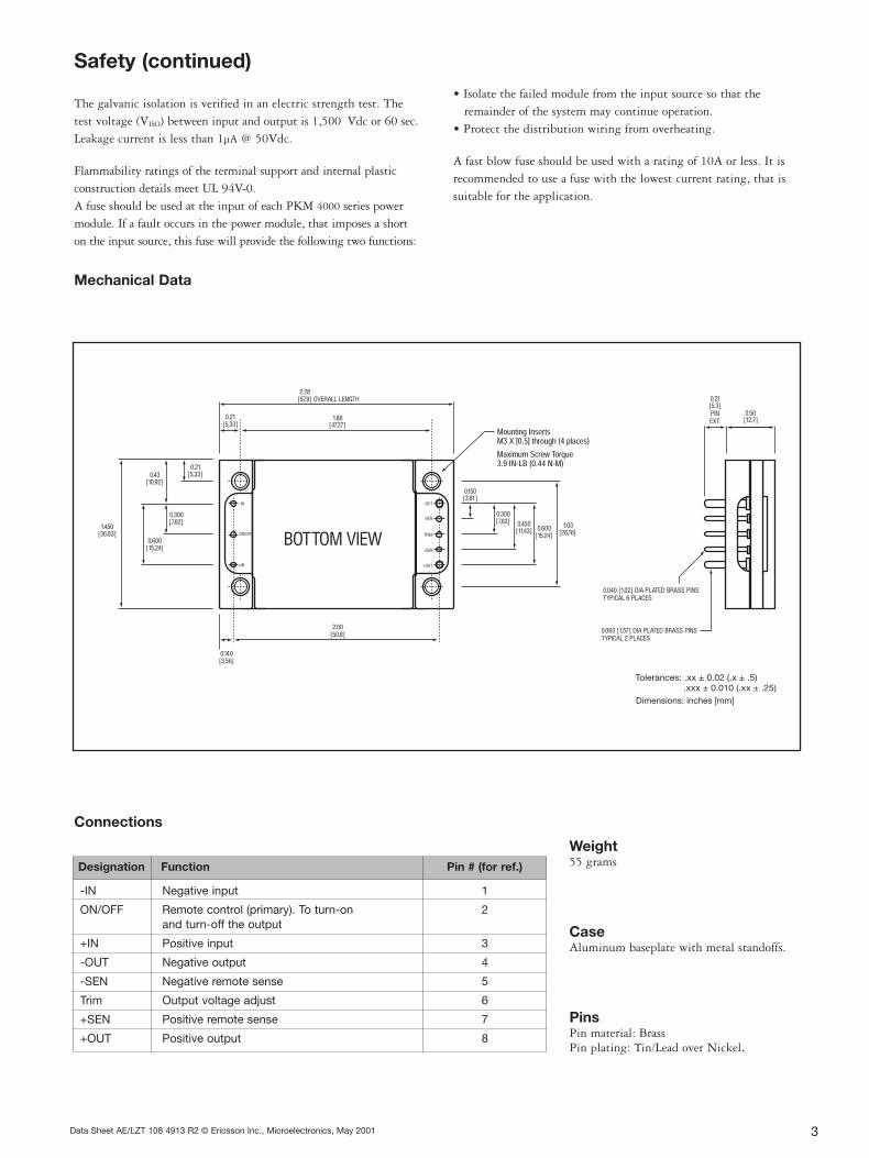
Safety
The PKM 4000 Series DC/DC power modules aredesigned in accordance with EN 60 950, Safety ofInformation Technology Equipment IncludingElectrical Business Equipment and are TUV TypeApproved.
The PKM 4000 DC/DC power modules are alsorecognized by UL and meet the applicablerequirements in UL 1950, Safety of InformationTechnology Equipment and applicable Canadiansafety requirements, i.e. ULc 1950.
The isolation is an operational insulation inaccordance with EN 60 950. The DC/DC powermodule should be installed in end-use equipment,in compliance with the requirements of theultimate application, and is intended to besupplied by an isolated secondary circuit.Consideration should be given to measuring thecase temperature to comply with TCmax when inoperation.
When the supply to the DC/DC powermodule meets all the requirements for SELV(<60Vdc), the output is considered to remainwithin SELV limits (level 3). If connected to a 60VDC power system, reinforced insulation must beprovided in the power supply that isolates theinput from the mains. Single fault testing in thepower supply must be performed in combinationwith the DC/DC power module to demonstratethat the output meets the requirement for SELV.One pole of the input and one pole of the output isto be grounded or both are to be kept floating.
3Data Sheet AE/LZT 108 4913 R2 © Ericsson Inc., Microelectronics, May 2001
Designation Function Pin # (for ref.)
-IN Negative input 1
ON/OFF Remote control (primary). To turn-on 2and turn-off the output
+IN Positive input 3
-OUT Negative output 4
-SEN Negative remote sense 5
Trim Output voltage adjust 6
+SEN Positive remote sense 7
+OUT Positive output 8
Connections
Weight55 grams
CaseAluminum baseplate with metal standoffs.
PinsPin material: BrassPin plating: Tin/Lead over Nickel.
Mechanical Data
Safety (continued)
The galvanic isolation is verified in an electric strength test. Thetest voltage (VISO) between input and output is 1,500 Vdc or 60 sec.Leakage current is less than 1µA @ 50Vdc.
Flammability ratings of the terminal support and internal plasticconstruction details meet UL 94V-0.A fuse should be used at the input of each PKM 4000 series powermodule. If a fault occurs in the power module, that imposes a short on the input source, this fuse will provide the following two functions:
• Isolate the failed module from the input source so that theremainder of the system may continue operation.
• Protect the distribution wiring from overheating.
A fast blow fuse should be used with a rating of 10A or less. It isrecommended to use a fuse with the lowest current rating, that issuitable for the application.

4 Data Sheet AE/LZT 108 4913 R2 © Ericsson Inc., Microelectronics, May 2001
0
0 10 20 30 40 50 60 70 80 90 100
5
10
15
20
Output Current Derating (No Heatsink) for 1.5V/20APKM4318PIOA
2.0 m/s
1.5 m/s
1.0 m/s
0.5 m/s
0.2 m/sNatural Convection
3.0 m/s
2.5 m/s
0 10 20 30 40 50 60 70 80 90 1000
5
10
15
Output Current Derating (No Heatsink) for 1.5V/15APKM4218PIOA
2.0 m/s
2.5 m/s
3.0 m/s
1.5 m/s
1.0 m/s
0.5 m/s
0.2 m/sNatural Convection
0 10 20 30 40 50 60 70 80 90 100
0
5
10
15
20
Output Current Derating (No Heatsink) for 1.8V/20APKM4318PI
2.0 m/s
1.5 m/s
1.0 m/s
0.5 m/s
0.2 m/sNatural Convection
3.0 m/s2.5 m/s
0 10 20 30 40 50 60 70 80 90 100
0
5
10
15
Output Current Derating (No Heatsink) for 1.8V/15APKM4218PI
2.0 m/s
2.5 m/s3.0 m/s
1.5 m/s1.0 m/s0.5 m/s0.2 m/sNatural Convection
0 10 20 30 40 50 60 70 80 90 100
0
5
10
15
20
Output Current Derating (No Heatsink) for 2.5V/20APKM4519PI
2.0 m/s
1.5 m/s
1.0 m/s
0.5 m/s
0.2 m/sNatural Convection
3.0 m/s2.5 m/s
0 10 20 30 40 50 60 70 80 90 100
0
5
10
15
Output Current Derating (No Heatsink) for 2.5V/15APKM4319PI
2.0 m/s
2.5 m/s3.0 m/s
1.5 m/s1.0 m/s0.5 m/s0.2 m/sNatural Convection
Airflow Conversion Tablem/s lfm
0.5 1001.0 2001.5 3002.0 4002.5 5003.0 600
Note: Natural Convection average airflow speed can vary from 0.05 m/s to 0.2 m/s.
Thermal DataThe PKM 4000 series DC/DC power modules has a robust thermaldesign which allows operation at case (baseplate) temperatures (TC)up to +100°C. The main cooling mechanism is convection (free orforced) through the case or optional heatsinks.
The graphs below show the allowable maximum output current tomaintain a maximum +100°C case temperature. Note that the ambienttemperature is the air temperature adjacent to the power module whichis typically elevated above the room environmental temperature.

0 10 20 30 40 50 60 70 80 90 100
0
5
10
15
20
Output Current Derating (No heatsink) for 3.3VPKM 4610PI and PKM 4510PI
1.5 m/s1.0 m/s0.5 m/s0.2 m/sNatural Convection
3.0 m/s2.5 m/s2.0 m/s
0
0 10 20 30 40 50 60 70 80 90 100
5
10
15
20
Output Current Derating (No Heatsink) for 5VPKM4111PI and PKM4711PI
1.0 m/s
0.5 m/s
0.2 m/sNatural Convection
3.0 m/s
2.5 m/s2.0 m/s1.5 m/s
5Data Sheet AE/LZT 108 4913 R2 © Ericsson Inc., Microelectronics, May 2001
Thermal DataThe graphs below can be used to estimate case temperatures for given system operating conditions (see Thermal Design).For further information on optional heatsinks, please contact your local Ericsson sales office.
0 10 20 30 40 50 60 70 80 90 100
6
5
4
3
2
1
0
Allowable Power Dissipation vs. Ambient Temp for 1.5VPKM4318PIOA and PKM4218PIOA
2.0 m/s
1.5 m/s
1.0 m/s
0.5 m/s
0.2 m/sNatural Convection
3.0 m/s
2.5 m/s
0 10 20 30 40 50 60 70 80 90 100
7
6
5
4
3
2
1
0
Allowable Power Dissipation vs. Ambient Temp for 1.8VPKM4318PI and PKM4218PI
2.0 m/s1.5 m/s
1.0 m/s0.5 m/s
0.2 m/sNatural Convection
3.0 m/s2.5 m/s
All Bending Points are at 5.5W
00 10 20 30 40 50 60 70 80 90 100
2
4
6
8
10
12
Allowable Power Dissipation vs. Ambient Temp for 3.3VPKM 4610PI and PKM 4510PI
1.5 m/s
1.0 m/s
0.5 m/s
0.2 m/sNatural Convection
3.0 m/s
2.5 m/s
2.0 m/s
0 10 20 30 40 50 60 70 80 90 100
9
8
7
6
5
4
3
2
1
0
Allowable Power Dissipation vs. Ambient Temp for 2.5VPKM4519PI and PKM4319PI
1.0 m/s0.5 m/s
0.2 m/sNatural Convection
3.0 m/s2.5 m/s
2.0 m/s
1.5 m/s
All Bending Points are at 6W
0 10 20 30 40 50 60 70 80 90 100
16
14
12
10
8
6
4
2
0
Allowable Power Dissipation vs. Ambient Temp for 5VPKM4111PI and PKM4711PI
1.0 m/s
0.5 m/s
0.2 m/sNatural Convection
3.0 m/s
2.5 m/s
2.0 m/s
1.5 m/s
Note: For conversion from m/s to lfm please see conversion table on pg. 4.

6 Data Sheet AE/LZT 108 4913 R2 © Ericsson Inc., Microelectronics, May 2001
Thermal Data
0 5 10 15
5
4
3
2
1
0
Power Dissipation vs. Output Current for 1.5V/15APKM4218PIOA
Vi=72v
Vi=60v
Vi=48v
Vi=36vPo
wer
Dis
sip
atio
n (
W)
Output Current (A)
0 5 10 15 20
7
6
5
4
3
2
1
0
Power Dissipation vs. Output Current for 1.8V/20APKM4318PI
Vi=72v
Vi=60v
Vi=48v
Vi=36v
Po
wer
Dis
sip
atio
n (
W)
Output Current (A)
0 5 10 15
Power Dissipation vs. Output Current for 1.8V/15APKM4218PI
Vi=72v
Vi=60v
Vi=48v
Vi=36vPo
wer
Dis
sip
atio
n (
W)
Output Current (A)
6
5
4
3
2
1
0
0 5 10 15 20
8
6
4
2
0
Power Dissipation vs. Output Current for 2.5V/20APKM4519PI
Vi=72v
Vi=60v
Vi=48v
Vi=36v
Po
wer
Dis
sip
atio
n (
W)
Output Current (A)
6
5
4
3
2
1
00 5 10 15
Power Dissipation vs. Output Current for 2.5V/15APKM4319PI
Vi=72v
Vi=60v
Vi=48v
Vi=36v
Po
wer
Dis
sip
atio
n (
W)
Output Current (A)
0 5 10 15 20
6
5
4
3
2
1
0
Power Dissipation vs. Output Current for 1.5V/20APKM4318PIOA
Vi=72v
Vi=60v
Vi=48v
Vi=36v
Po
wer
Dis
sip
atio
n (
W)
Output Current (A)

7Data Sheet AE/LZT 108 4913 R2 © Ericsson Inc., Microelectronics, May 2001
0 5 10 15
6
5
4
3
2
1
0
Power Dissipation vs. Output Current for 3.3V/15APKM4510PI
Vi=72v
Vi=60v
Vi=48v
Vi=36v
Po
wer
Dis
sip
atio
n (
W)
Output Current (A)
0 5 10 15 20
12
10
8
6
4
2
0
Power Dissipation vs. Output Current for 5V/20APKM4111PI
Vi=72v
Vi=60v
Vi=48v
Vi=36v
Po
wer
Dis
sip
atio
n (
W)
Output Current (A)
0 5 10 15
8
7
6
5
4
3
2
1
0
Power Dissipation vs. Output Current for 5V/15APKM4711PI
Vi=72v
Vi=60v
Vi=48v
Vi=36v
Po
wer
Dis
sip
atio
n (
W)
Output Current (A)
Thermal Data
00 5 10 15 20
2
4
6
8
10
Power Dissipation vs. Output Current for 3.3V/20APKM4610PI
Vi=72v
Vi=60v Vi=48v
Vi=36vPo
wer
Dis
sip
atio
n (
W)
Output Current (A)

8 Data Sheet AE/LZT 108 4913 R2 © Ericsson Inc., Microelectronics, May 2001
00 0.5 1 1.5 2 32.5
2
4
6
8
10
Air Flow (m/s)
Case to Ambient Thermal Resistance
PKM 4000 Series
Thermal DesignThe thermal data can be used to determine thermal performance without a heatsink.
Case temperature is calculated by the following formula:
TC = TA + Pd x RthC-A (˚C/W)where Pd = PO(1/η - 1)Where:TC: Case TemperatureTA: Local Ambient Temperature Pd: Dissipated PowerRthC-A: Thermal Resistance from TC to TA
Po: Output Powerη: EfficiencyThe efficiency η can be found in the tables on the following pages.
For design margin and to enhance system reliability, it is recommendedthat the PKM 4000 series DC/DC power modules are operated at casetemperatures below 90°C.

9Data Sheet AE/LZT 108 4913 R2 © Ericsson Inc., Microelectronics, May 2001
PKM 4318 PIOA (30W)TC = -40...+100°C, VI = 36...75V dc unless otherwise specified.
Characteristics Conditions Output
min typ max Unit
VOi Output voltage initial TC = +25°C, VI = 53V, IO = IOmax 1.48 1.5 1.52 Vsetting and accuracy
Output adjust range IO = 0 to IOmax 1.2 1.66 V
VO Output voltage IO = 0 to IOmax 1.43 1.58 Vtolerance band
Line regulation IO = IOmax 3 10 mV
Load regulation VI = 53V, IO = 0 to IOmax 3 10 mV
Vtr Load transient Load step = 0.25 x IOmax ±150 mVpeak
voltage deviation dI/dt = 1A/µs
ttr Load transient 100 µsrecovery time
ts Start-up time From VI connection to VO = 0.9 x VOnom 25 40 ms
IO Output current 0 20 A
POmax Max output power At VO = VOnom 30 W
IIim Current limit threshold VO = 0.96 VOnom @ TC<100°C 21 24 26 A
ISC Short circuit current 24 28 A
VOac Output ripple and noise IO = IOmax f < 20 MHz 70 150 mVp-p
SVR Supply voltage f<1kHz -53 dBrejection (ac)
OVP Over voltage protection Vin = 50V 2.2 2.5 2.8 V
Output
Characteristics Conditions min typ max Unit
η Efficiency TA = +25°C, VI = 53V, IO = IOmax 87 %
Pd Power dissipation TA = +25°C, VI = 53V, IO = IOmax 4.5 W
fO Switching frequency IO = 0...1.0 x IOmax 200 kHz
Miscellaneous
10 Data Sheet AE/LZT 108 4913 R2 © Ericsson Inc., Microelectronics, May 2001
PKM 4218 PIOA (22.5W)TC = -40...+100°C, VI = 36...75V dc unless otherwise specified.
Characteristics Conditions Output
min typ max Unit
VOi Output voltage initial TC = +25°C, VI = 53V, IO = IOmax 1.48 1.5 1.52 Vsetting and accuracy
Output adjust range IO = 0 to IOmax 1.2 1.66 V
VO Output voltage IO = 0 to IOmax 1.43 1.58 Vtolerance band
Line regulation IO = IOmax 3 10 mV
Load regulation VI = 53V, IO = 0 to IOmax 3 10 mV
Vtr Load transient Load step = 0.25 x IOmax ±150 mVpeak
voltage deviation dI/dt = 1A/µs
ttr Load transient 100 µsrecovery time
ts Start-up time From VI connection to VO = 0.9 x VOnom 25 40 ms
IO Output current 0 15 A
POmax Max output power At VO = VOnom 22.5 W
IIim Current limit threshold VO = 0.96 VOnom @ TC<100°C 16 18 21 A
ISC Short circuit current 20 23 A
VOac Output ripple and noise IO = IOmax f < 20 MHz 70 150 mVp-p
SVR Supply voltage f<1kHz -53 dBrejection (ac)
OVP Over voltage protection Vin = 50V 2.2 2.5 2.8 V
Output
Characteristics Conditions min typ max Unit
η Efficiency TA = +25°C, VI = 53V, IO = IOmax 87 %
Pd Power dissipation TA = +25°C, VI = 53V, IO = IOmax 3.4 W
fO Switching frequency IO = 0...1.0 x IOmax 200 kHz
Miscellaneous
11Data Sheet AE/LZT 108 4913 R2 © Ericsson Inc., Microelectronics, May 2001
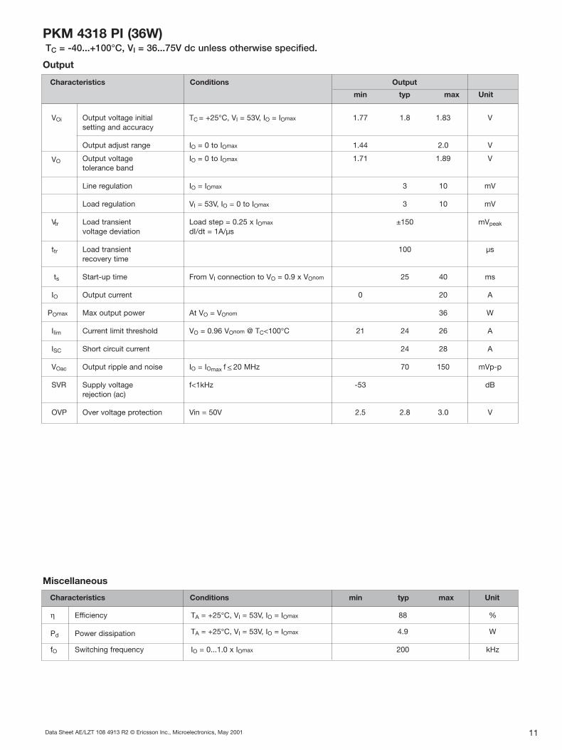
PKM 4318 PI (36W)TC = -40...+100°C, VI = 36...75V dc unless otherwise specified.
Characteristics Conditions Output
min typ max Unit
VOi Output voltage initial TC = +25°C, VI = 53V, IO = IOmax 1.77 1.8 1.83 Vsetting and accuracy
Output adjust range IO = 0 to IOmax 1.44 2.0 V
VO Output voltage IO = 0 to IOmax 1.71 1.89 Vtolerance band
Line regulation IO = IOmax 3 10 mV
Load regulation VI = 53V, IO = 0 to IOmax 3 10 mV
Vtr Load transient Load step = 0.25 x IOmax ±150 mVpeak
voltage deviation dI/dt = 1A/µs
ttr Load transient 100 µsrecovery time
ts Start-up time From VI connection to VO = 0.9 x VOnom 25 40 ms
IO Output current 0 20 A
POmax Max output power At VO = VOnom 36 W
IIim Current limit threshold VO = 0.96 VOnom @ TC<100°C 21 24 26 A
ISC Short circuit current 24 28 A
VOac Output ripple and noise IO = IOmax f < 20 MHz 70 150 mVp-p
SVR Supply voltage f<1kHz -53 dBrejection (ac)
OVP Over voltage protection Vin = 50V 2.5 2.8 3.0 V
Output
Characteristics Conditions min typ max Unit
η Efficiency TA = +25°C, VI = 53V, IO = IOmax 88 %
Pd Power dissipation TA = +25°C, VI = 53V, IO = IOmax 4.9 W
fO Switching frequency IO = 0...1.0 x IOmax 200 kHz
Miscellaneous
12 Data Sheet AE/LZT 108 4913 R2 © Ericsson Inc., Microelectronics, May 2001
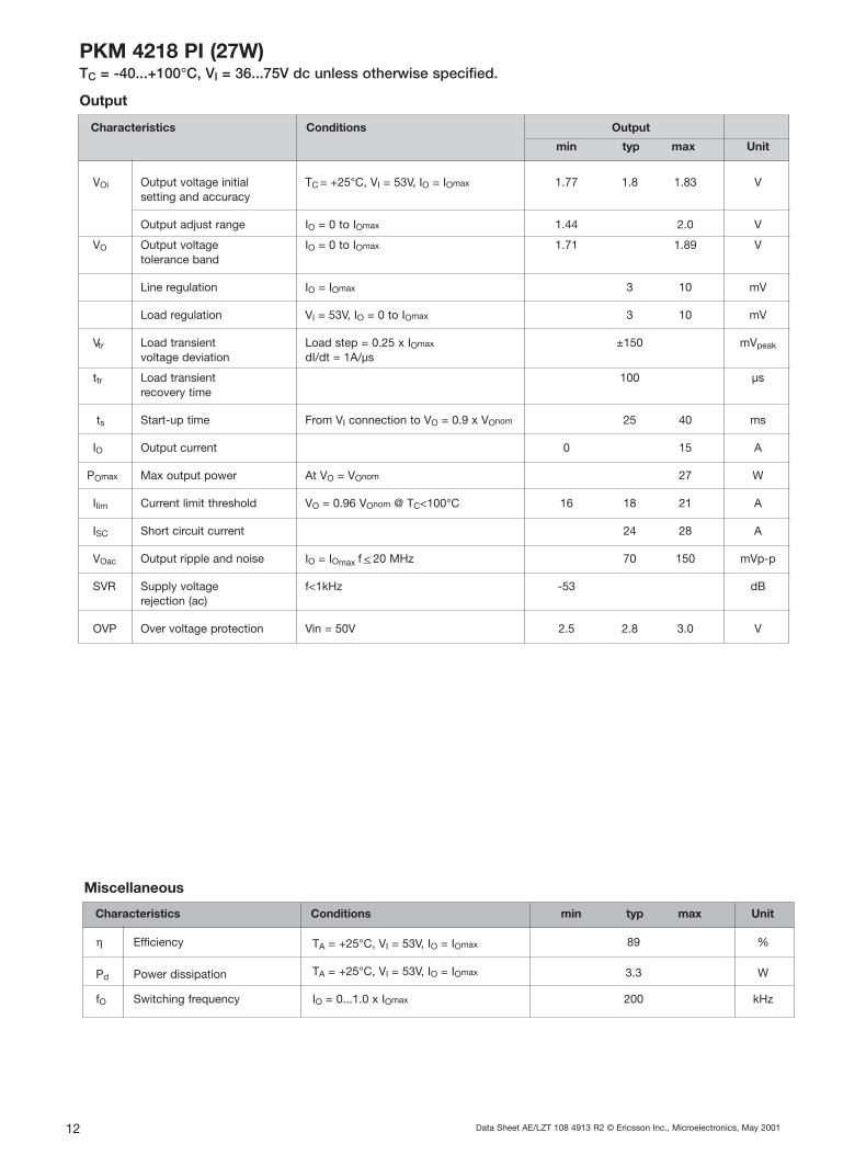
PKM 4218 PI (27W)TC = -40...+100°C, VI = 36...75V dc unless otherwise specified.
Characteristics Conditions Output
min typ max Unit
VOi Output voltage initial TC = +25°C, VI = 53V, IO = IOmax 1.77 1.8 1.83 Vsetting and accuracy
Output adjust range IO = 0 to IOmax 1.44 2.0 V
VO Output voltage IO = 0 to IOmax 1.71 1.89 Vtolerance band
Line regulation IO = IOmax 3 10 mV
Load regulation VI = 53V, IO = 0 to IOmax 3 10 mV
Vtr Load transient Load step = 0.25 x IOmax ±150 mVpeak
voltage deviation dI/dt = 1A/µs
ttr Load transient 100 µsrecovery time
ts Start-up time From VI connection to VO = 0.9 x VOnom 25 40 ms
IO Output current 0 15 A
POmax Max output power At VO = VOnom 27 W
IIim Current limit threshold VO = 0.96 VOnom @ TC<100°C 16 18 21 A
ISC Short circuit current 24 28 A
VOac Output ripple and noise IO = IOmax f < 20 MHz 70 150 mVp-p
SVR Supply voltage f<1kHz -53 dBrejection (ac)
OVP Over voltage protection Vin = 50V 2.5 2.8 3.0 V
Output
Characteristics Conditions min typ max Unit
η Efficiency TA = +25°C, VI = 53V, IO = IOmax 89 %
Pd Power dissipation TA = +25°C, VI = 53V, IO = IOmax 3.3 W
fO Switching frequency IO = 0...1.0 x IOmax 200 kHz
Miscellaneous

13Data Sheet AE/LZT 108 4913 R2 © Ericsson Inc., Microelectronics, May 2001
PKM 4519 PI (50W)TC = -40...+100°C, VI = 36...75V dc unless otherwise specified.
Characteristics Conditions Output
min typ max Unit
VOi Output voltage initial TC = +25°C, VI = 53V, IO = IOmax 2.45 2.5 2.55 Vsetting and accuracy
Output adjust range IO = 0 to IOmax 2.0 2.75 V
VO Output voltage IO = 0 to IOmax 2.4 2.6 Vtolerance band
Line regulation IO = IOmax 3 10 mV
Load regulation VI = 53V, IO = 0 to IOmax 3 10 mV
Vtr Load transient Load step = 0.25 x IOmax ±150 mVpeak
voltage deviation dI/dt = 1A/µs
ttr Load transient 100 µsrecovery time
ts Start-up time From VI connection to VO = 0.9 x VOnom 25 40 ms
IO Output current 0 20 A
POmax Max output power At VO = VOnom 50 W
IIim Current limit threshold VO = 0.96 VOnom @ TC<100°C 21 24 26 A
ISC Short circuit current 26 30 A
VOac Output ripple and noise IO = IOmax f < 20 MHz 60 100 mVp-p
SVR Supply voltage f<1kHz -53 dBrejection (ac)
OVP Over voltage protection Vin = 50V 3.2 3.7 4.2 V
Output
Characteristics Conditions min typ max Unit
η Efficiency TA = +25°C, VI = 53V, IO = IOmax 89 %
Pd Power dissipation TA = +25°C, VI = 53V, IO = IOmax 6.2 W
fO Switching frequency IO = 0...1.0 x IOmax 200 kHz
Miscellaneous

14 Data Sheet AE/LZT 108 4913 R2 © Ericsson Inc., Microelectronics, May 2001
PKM 4319 PI (37.5W)TC = -40...+100°C, VI = 36...75V dc unless otherwise specified.
Characteristics Conditions Output
min typ max Unit
VOi Output voltage initial TC = +25°C, VI = 53V, IO = IOmax 2.45 2.5 2.55 Vsetting and accuracy
Output adjust range IO = 0 to IOmax 2.0 2.75 V
VO Output voltage IO = 0 to IOmax 2.4 2.6 Vtolerance band
Line regulation IO = IOmax 3 10 mV
Load regulation VI = 53V, IO = 0 to IOmax 3 10 mV
Vtr Load transient Load step = 0.25 x IOmax ±150 mVpeak
voltage deviation dI/dt = 1A/µs
ttr Load transient 100 µsrecovery time
ts Start-up time From VI connection to VO = 0.9 x VOnom 25 40 ms
IO Output current 0 15 A
POmax Max output power At VO = VOnom 37.5 W
IIim Current limit threshold VO = 0.96 VOnom @ TC<100°C 16 18 21 A
ISC Short circuit current 26 30 A
VOac Output ripple and noise IO = IOmax f < 20 MHz 60 100 mVp-p
SVR Supply voltage f<1kHz -53 dBrejection (ac)
OVP Over voltage protection Vin = 50V 3.2 3.7 4.2 V
Output
Characteristics Conditions min typ max Unit
η Efficiency TA = +25°C, VI = 53V, IO = IOmax 89 %
Pd Power dissipation TA = +25°C, VI = 53V, IO = IOmax 4.6 W
fO Switching frequency IO = 0...1.0 x IOmax 200 kHz
Miscellaneous

15Data Sheet AE/LZT 108 4913 R2 © Ericsson Inc., Microelectronics, May 2001
Characteristics Conditions Output
min typ max Unit
VOi Output voltage initial TC = +25°C, VI = 53V, IO = IOmax 3.25 3.30 3.35 Vsetting and accuracy
Output adjust range IO = 0 to IOmax 2.64 3.63 V
VO Output voltage IO = 0 to IOmax 3.2 3.4 Vtolerance band
Line regulation IO = IOmax 3 10 mV
Load regulation VI = 53V, IO = 0 to IOmax 3 10 mV
Vtr Load transient Load step = 0.25 x IOmax ±150 mVpeakvoltage deviation dI/dt = 1A/µs
ttr Load transient 100 µsrecovery time
ts Start-up time From VI connection to VO = 0.9 x VOnom 25 40 ms
IO Output current 0 20 A
POmax Max output power At VO = VOnom 66 W
Ilim Current limit threshold VO = 0.90 x VOnom @ TC<100°C 21 24 26 A
ISC Short circuit current 24 28 A
VOac Output ripple and noise IO = IOmax f < 20 MHz 60 100 mVp-p
SVR Supply voltage f<1 kHz -53 dBrejection
OVP Overvoltage protection VI = 53V 3.9 4.4 5.0 V
Output
PKM 4610 PI (66W)
TC = -40...+100°C, VI = 36...75V dc unless otherwise specified.
Characteristics Conditions min typ max Unit
η Efficiency TA = +25°C, VI = 53V, IO = IOmax 89 %
Pd Power dissipation TA = +25°C, VI = 53V, IO = IOmax 8.2 W
fO Switching frequency IO = 0...1.0 x IOmax 150 kHz
Miscellaneous

Characteristics Conditions Output
min typ max Unit
VOi Output voltage initial TC = +25°C, VI = 53V, IO = IOmax 3.25 3.30 3.35 Vsetting and accuracy
Output adjust range IO = 0 to IOmax 2.64 3.63 V
VO Output voltage IO = 0 to IOmax 3.2 3.4 Vtolerance band
Line regulation IO = IOmax 3 10 mV
Load regulation VI = 53V, IO = 0 to IOmax 3 10 mV
Vtr Load transient Load step = 0.25 x IOmax ±150 mVpeakvoltage deviation dI/dt = 1A/µs
ttr Load transient 100 µsrecovery time
ts Start-up time From VI connection to VO = 0.9 x VOnom 25 40 ms
IO Output current 0 15 A
POmax Max output power At VO = VOnom 50 W
Ilim Current limit threshold VO = 0.90 x VOnom @ TC<100°C 16 18 21 A
ISC Short circuit current 20 23 A
VOac Output ripple and noise IO = IOmax f < 20 MHz 60 100 mVp-p
SVR Supply voltage f<1 kHz -53 dBrejection
OVP Overvoltage protection VI = 53V 3.9 4.4 5.0 V
Output
PKM 4510 PI (50W)TC = -40...+100°C, VI = 36...75V dc unless otherwise specified.
16 Data Sheet AE/LZT 108 4913 R2 © Ericsson Inc., Microelectronics, May 2001
Characteristics Conditions min typ max Unit
η Efficiency TA = +25°C, VI = 53V, IO = IOmax 91 %
Pd Power dissipation TA = +25°C, VI = 53V, IO = IOmax 4.9 W
fO Switching frequency IO = 0...1.0 x IOmax 150 kHz
Miscellaneous

17Data Sheet AE/LZT 108 4913 R2 © Ericsson Inc., Microelectronics, May 2001
Characteristics Conditions Output
min typ max Unit
VOi Output voltage initial TC = +25°C, VI = 53V, IO = IOmax 4.9 5.0 5.1 Vsetting and accuracy
Output adjust range IO = 0 to IOmax, VI = 38...75V dc 4.0 5.5 V
VO Output voltage IO = 0 to IOmax 4.85 5.15 Vtolerance band
Line regulation VI = 38...75V, IO = IOmax 3 10 mV
Load regulation VI = 53V, IO = 0 to IOmax 3 10 mV
Vtr Load transient Load step = 0.25 x IOmax ±150 mVpeak
voltage deviation dI/dt = 1A/µs
ttr Load transient 200 µsrecovery time
ts Start-up time From VI connection to VO = 0.9 x VOnom 60 90 ms
IO Output current 0 20 A
POmax Max output power At VO = VOnom 100 W
IIim Current limit threshold VO = 0.96 VOnom @ TC<100°C 21 24 26 A
ISC Short circuit current 24 28 A
VOac Output ripple and noise IO = IOmax f < 20 MHz 85 150 mVp-p
SVR Supply voltage f<1kHz -53 dBrejection (ac)
OVP Over voltage protection Vin = 50V 5.8 6.2 6.5 V
Output
Characteristics Conditions min typ max Unit
η Efficiency TA = +25°C, VI = 53V, IO = IOmax 90 %
Pd Power dissipation TA = +25°C, VI = 53V, IO = IOmax 11.1 W
fO Switching frequency IO = 0...1.0 x IOmax 200 kHz
Miscellaneous
PKM 4111 PI (100W)TC = -40...+100°C, VI = 36...75V dc unless otherwise specified.

18 Data Sheet AE/LZT 108 4913 R2 © Ericsson Inc., Microelectronics, May 2001
Characteristics Conditions Output
min typ max Unit
VOi Output voltage initial TC = +25°C, VI = 53V, IO = IOmax 4.9 5.0 5.1 Vsetting and accuracy
Output adjust range IO = 0 to IOmax, VI = 38...75V dc 4.0 5.5 V
VO Output voltage IO = 0 to IOmax 4.85 5.15 Vtolerance band
Line regulation VI = 38...75V, IO = IOmax 3 10 mV
Load regulation VI = 53V, IO = 0 to IOmax 3 10 mV
Vtr Load transient Load step = 0.25 x IOmax ±150 mVpeak
voltage deviation dI/dt = 1A/µs
ttr Load transient 200 µsrecovery time
ts Start-up time From VI connection to VO = 0.9 x VOnom 60 90 ms
IO Output current 0 15 A
POmax Max output power At VO = VOnom 75 W
IIim Current limit threshold VO = 0.96 VOnom @ TC<100°C 16 18 21 A
ISC Short circuit current 24 28 A
VOac Output ripple and noise IO = IOmax f < 20 MHz 85 150 mVp-p
SVR Supply voltage f<1kHz -53 dBrejection (ac)
OVP Over voltage protection Vin = 50V 5.8 6.2 6.5 V
Output
Characteristics Conditions min typ max Unit
η Efficiency TA = +25°C, VI = 53V, IO = IOmax 92 %
Pd Power dissipation TA = +25°C, VI = 53V, IO = IOmax 6.5 W
fO Switching frequency IO = 0...1.0 x IOmax 200 kHz
Miscellaneous
PKM 4711 PI (75W)TC = -40...+100°C, VI = 36...75V dc unless otherwise specified.

19Data Sheet AE/LZT 108 4913 R2 © Ericsson Inc., Microelectronics, May 2001
PKM 4318 PIOA (30W)
PKM 4218 PIOA (22.5W)
5 10 15 2060
65
70
75
80
85
90
95
36V48V60V72V
Efficiency
Output Current (A)
Eff
icie
ncy
(%
)
0 5 10 15 20 25 300
1
2
3
Output Characteristics
Output Current (A)
Ou
tpu
t Vo
ltag
e (V
)
(48Vin)
5 10 1560
65
70
75
80
85
90
95
36V48V60V72V
Efficiency
Output Current (A)
Eff
icie
ncy
(%
)
0 5 10 15 20 250
1
2
3
Output Characteristics
Output Current (A)
Ou
tpu
t Vo
ltag
e (V
)
(48Vin)

20 Data Sheet AE/LZT 108 4913 R2 © Ericsson Inc., Microelectronics, May 2001
PKM 4318 PI (36W)
PKM 4218 PI (27W)
5 10 15 2060
65
70
75
80
85
90
95
36V48V60V72V
Efficiency
Output Current (A)
Eff
icie
ncy
(%
)
0 5 10 15 20 25 300
1
2
3
Output Characteristics
Output Current (A)
Ou
tpu
t Vo
ltag
e (V
)
(48Vin)
5 10 1560
65
70
75
80
85
90
95
36V48V60V72V
Efficiency
Output Current (A)
Eff
icie
ncy
(%
)
0 5 10 15 20 250
1
2
3
Output Characteristics
Output Current (A)
Ou
tpu
t Vo
ltag
e (V
)
(48Vin)

21Data Sheet AE/LZT 108 4913 R2 © Ericsson Inc., Microelectronics, May 2001
PKM 4519 (50W)
PKM 4319 PI (37.5W)
5 10 15 2072
74
76
78
80
82
84
86
88
90
92
36V48V60V72V
Efficiency
Output Current (A)
Eff
icie
ncy
(%
)
0 5 10 15 20 25 300
1
2
3
Output Characteristics
Output Current (A)
Ou
tpu
t Vo
ltag
e (V
)
(48Vin)
5 10 1572
74
76
78
80
82
84
86
88
90
92
36V48V60V72V
Efficiency
Output Current (A)
Eff
icie
ncy
(%
)
0 5 10 15 20 250
1
2
3
Output Characteristics
Output Current (A)
Ou
tpu
t Vo
ltag
e (V
)
(48Vin)

22 Data Sheet AE/LZT 108 4913 R2 © Ericsson Inc., Microelectronics, May 2001
PKM 4610 PI (66W)
PKM 4510 PI (50W)
5 10 15 2082
84
86
88
90
92
94
36V48V60V72V
Efficiency
Output Current (A)
Eff
icie
ncy
(%
)
0 5 10 15 20 250
1
2
3
4
Output Characteristics
Output Current (A)
Ou
tpu
t Vo
ltag
e (V
)
(48Vin)
5 10 1582
84
86
88
90
92
94
36V48V60V72V
Efficiency
Output Current (A)
Eff
icie
ncy
(%
)
0 5 10 15 20 250
1
2
3
4
Output Characteristics
Output Current (A)
Ou
tpu
t Vo
ltag
e (V
)
(48Vin)

23Data Sheet AE/LZT 108 4913 R2 © Ericsson Inc., Microelectronics, May 2001
PKM 4111 PI (100W)
PKM 4711 PI (75W)
5 10 15 2082
84
86
88
90
92
94
36V48V60V72V
Efficiency
Output Current (A)
Eff
icie
ncy
(%
)
0 5 10 15 20 25 300
1
2
3
4
5
6
Output Characteristics
Output Current (A)
Ou
tpu
t Vo
ltag
e (V
)
(48Vin)
5 10 1582
84
86
88
90
92
94
36V48V60V72V
Efficiency
Output Current (A)
Eff
icie
ncy
(%
)
0 5 10 15 20 250
1
2
3
4
5
6
Output Characteristics
Output Current (A)
Ou
tpu
t Vo
ltag
e (V
)
(48Vin)

EMC Specifications
The PKM power module is mounted on a double sided printed circuit board PCB with groundplane during EMC measurements.The fundamental switching frequency is 150 kHz @ IO = IOmax.
Conducted EMIInput terminal value with 100µF capacitor (typ) and additional PI filter.
0.68µF
L1
L3
L2
0.68µF
0.68µF
47µF
10nF4.7nF
4.7nF
3.3nF
3.3nF
47µF
10nF
External Filter (class B)
Required external input filter in order to meet class B in EN 55022, CISPR 22 and FCC part 15J.
L1: 450µH TDK TF1028S-451Y3R-01L2 & L3: 22µH Coilcraft D05ø22P-23*The baseplate is floated.
24 Data Sheet AE/LZT 108 4913 R2 © Ericsson Inc., Microelectronics, May 2001
Class A
Class B

25Data Sheet AE/LZT 108 4913 R2 © Ericsson Inc., Microelectronics, May 2001
Remote Sense
All PKM 4000 series DC/DC power modules have remote sensethat can be used to compensate for moderate amounts of resistancein the distribution system and allow for voltage regulation at theload or other selected point. The remote sense lines will carry verylittle current and do not need a large cross sectional area. However,the sense lines on a PCB should be located close to a ground traceor ground plane. In a discrete wiring situation, the usage oftwisted pair wires or other technique for reducing noisesusceptibility is recommended.
The power module will compensate for up to 0.5V voltage dropbetween the sense voltage and the voltage at the power moduleoutput pins. The output voltage and the remote sense voltageoffset must be less than the minimum overvoltage trip point.
Current LimitingGeneral Characteristics
All PKM 4000 series DC/DC power modules include currentlimiting circuitry that makes them able to withstand continuousoverloads or short circuit conditions on the output. The outputvoltage will decrease toward zero for heavy overloads.
The power module will resume normal operation after removal ofthe overload. The load distribution system should be designed tocarry the maximum short circuit output current specified.
Operating Information
Input Voltage
The input voltage range 36...75V meets the requirements in theEuropean Telecom Standard ETS 300 132-2 for normal inputvoltage range in -48V and -60V DC power systems, -40.5...-57.0Vand -50.0...-72.0V respectively. At input voltages exceeding 75V,the power loss will be higher than at normal input voltage and TC
must be limited to absolute max +100º C. The absolute maxcontinuous input voltage is 80V DC.
Remote Control (RC)
The PKM 4000 series DC/DC power modules have two remoteon/off options available. Negative logic remote on/off is the standardoption orderable without a suffix added to the part number.Negative logic remote on/off turns the module off during a logichigh voltage on the on/off pin, and on during a logic low state.Positive logic remote on/off is orderable by adding the suffix “P” tothe end of the part number. Positive logic remote on/off turns themodule on during a logic high and off during a logic low state.
The RC pin can be wired directly to -In, to allow the module topower up automatically without the need for control signals.
A mechanical switch or an open collector transistor or FET can beused to drive the RC inputs. The device must be capable ofsinking up to 1mA at a low level voltage of 1.0V, maximum of15V dc, for the primary RC.
RC (primary) Power module
Low ONOpen/High OFF
Over Voltage Protection (OVP)
All PKM 4000 DC/DC power modules have latching outputovervoltage protection. In the event of an overvoltage condition, thepower module will shut down. The power module can be restartedby cycling the input voltage.
Turn-(on/off) Input Voltage (VIon/VIoff)
The power module monitors the input voltage and will turn on andturn off at predetermined levels. See Input Table on page 2.
Output Voltage Adjust (Trim)Voltage Trimming
All PKM 4000 series DC/DC power modules have an OutputVoltage Adjust pin. This pin can be used to adjust the outputvoltage above or below VOi. When increasing the output voltage,the voltage at the output pins (including any remote sensing offset)must be kept below the overvoltage trip point. Also note that atelevated output voltages the maximum power rating of the moduleremains the same, and the output current capability will decreasecorrespondingly. These modules trim exactly like the other majorcompetitors quarter-brick modules.To decrease VO connect Radj from - SEN to TrimTo increase VO connect Radj from + SEN to Trim
Standard Remote ControlRC (primary) Power module
Low OFFOpen/High ON
Optional Remote Control (P)

26
Output Voltage Trim for 1.8V
Ad
just
res
isto
r Val
ue
(k O
hm
)
Change in Output Voltage (∆%)
1
0 2 4 6 8 10 12 14 16 18 20
100
10
1000
10000
100000
Decrease
Increase
Output Voltage Trim for 2.5V
Ad
just
res
isto
r V
alu
e(k
Oh
m)
Change in Output Voltage (˘%)
1
0 2 4 6 8 10 12 14 16 18 20
100
10
1000
10000
100000
Decrease
Increase
Output Voltage Trim for 3.3V
Ad
just
res
isto
r V
alu
e(k
Oh
m)
Change in Output Voltage (˘%)
1
0 2 4 6 8 10 12 14 16 18 20
100
10
1000
10000
100000
Decrease
Increase
Output Voltage Trim for 5.0V
Ad
just
res
isto
r V
alu
e(k
Oh
m)
Change in Output Voltage (˘%)
10 2 4 6 8 10 12 14 16 18 20
100
10
1000
10000
1000000
100000
Decrease
Increase
Output Voltage Trim for 1.5V
Ad
just
res
isto
r Val
ue
(k O
hm
)
Change in Output Voltage (∆%)
1
0 2 4 6 8 10 12 14 16 18 20
100
10
1000
10000
100000
Decrease
Increase
Decrease: Radj = 5.11( 100 -2)kΩ∆%
Increase: Radj = 5.11[ Vo (100+∆%) - (100+2∆%) ]kΩ1.225∆% ∆%
Decrease: Radj = 5.11( 100 -2)kΩ∆%
Increase: Radj = 5.11[ Vo (100+∆%) - (100+2∆%) ]kΩ1.225∆% ∆%
Decrease: Radj = 5.11( 100 -2)kΩ∆%
Increase: Radj = 5.11[ Vo (100+∆%) - (100+2∆%) ]kΩ1.225∆% ∆%
Decrease: Radj = 5.11( 100 -2)kΩ∆%
Increase: Radj = 5.11[ Vo (100+∆%) - (100+2∆%) ]kΩ1.225∆% ∆%
Decrease: Radj = 5.11( 100 -2)kΩ∆%
Increase: Radj = 5.11[ Vo (100+∆%) - (100+2∆%) ]kΩ1.225∆% ∆%
Data Sheet AE/LZT 108 4913 R2 © Ericsson Inc., Microelectronics, May 2001

Paralleling for Redundancy
The figure below shows how n + 1 redundancy can be achieved. Thediodes on the power module outputs allow a failed module to removeitself from the shared group without pulling down the common outputbus. This configuration can be extended to additional numbers ofpower modules and they can also be controlled individually or ingroups by means of signals to the primary RC inputs.
Output Ripple & Noise (VOac)
Output ripple is measured as the peak to peak voltage from 0 to20MHz which includes the noise voltage and fundamental ripple.
Over Temperature Protection
The PKM 4000 DC/DC power modules are protected from thermaloverload by an internal over temperature shutdown circuit. When thecase temperature exceeds +110°C (+10, -5°C), the power module willautomatically shut down (latching). To restart the module the inputvoltage must be cycled.
Input and Output Impedance
The impedance of both the power source and the load will interactwith the impedence of the DC/DC power module. It is most importantto have the ratio between L and C as low as possible, i.e. a lowcharacteristic impedance, both at the input and output, as the powermodules have a low energy storage capability. The PKM 4000 series ofDC/DC power modules has been designed to be completely stablewithout the need for external capacitors on the input or output whenconfigured with low inductance input and output circuits. Theperformance in some applications can be enhanced by the addition ofexternal capacitance as described below. If the distribution of the inputvoltage source to the power module contains significant inductance,the addition of a 220-470 µF capacitor across the input of the powermodule will help insure stability. This capacitor is not required whenpowering the module from a low impedance source with short, lowinductance, input power leads.
Output Capacitance
When powering loads with significant dynamic current requirements,the voltage regulation at the load can be improved by the addition ofdecoupling capacitance at the load. The most effective technique is tolocate low ESR ceramic capacitors as close to the load as possible, usingseveral capacitors to lower the effective ESR. These ceramic capacitorswill handle the short duration high frequency components of thedynamic current requirement. In addition, higher values of electrolyticcapacitors should be used to handle the mid-frequency components. Itis equally important to use good design practices when configuring theDC distribution system.
27Data Sheet AE/LZT 108 4913 R2 © Ericsson Inc., Microelectronics, May 2001
Low resistance and low inductance PCB (printed circuit board) layoutsand cabling should be used. Remember that when using remotesensing, all the resistance, inductance and capacitance of thedistribution system is within the feedback loop of the power module.This can have an effect on the modules compensation and the resultingstability and dynamic response performance.
As a rule of thumb, 100 µF/A of output current can be used withoutany additional analysis. For example, with a 20A (max PO 100W)power module, values of decoupling capacitance up to 2000 µF can beused without regard to stability. With larger values of capacitance, theload transient recovery time can exceed the specified value. As much ofthe capacitance as possible should be outside of the remote sensingloop and close to the load.The absolute maximum value of outputcapacitance is 10,000 µF. For values larger than this contact your localEricsson representative.
Quality
Reliability
The calculated MTBF of the PKM 4000 module family is greater than(>) 2.8 million hours using Bellcore TR-332 methodology. Thecalculation is valid for a 90ºC baseplate temperature. DemonstratedMTBF has been in the range of 3.0 to 3.2 million hours.
Quality Statement
The power modules are designed and manufactured in an industrialenvironment where quality systems and methods like ISO 9000, 6σ,and SPC, are intensively in use to boost the continuous improvementsstrategy. Infant mortality or early failures in the products are screenedout and they are subjected to an ATE-based final test.Conservative design rules, design reviews and product qualifications,plus the high competence of an engaged work force, contribute to thehigh quality of our products.
Warranty
Ericsson Inc., Microelectronics warrants to the original purchaser orend user that the products conform to this Data Sheet and are freefrom material and workmanship defects for a period of five (5) yearsfrom the date of manufacture, if the product is used within specifiedconditions and not opened.In case the product is discontinued, claims will be accepted up to three(3) years from the date of the discontinuation. For additional details onthis limited warranty we refer to Ericsson’s “General Terms andConditions of Sales,” EKA 950701, or individual contract documents.
Limitation of Liability
Ericsson Inc., Microelectronics does not make any other warranties,expressed or implied including any warranty of merchantability orfitness for a particular purpose (including, but not limited to use in life support applications, where malfunctions of product can causeinjury to a person’s health or life).
PKM
PKM1 PKM2

The PKM DC/DC power module may be ordered with the different optionslisted in the Product Options table.
Ericsson Inc.Microelectronics1700 International Pkwy., Suite 200Richardson, Texas 75081Phone: 877-ERICMICwww.ericsson.com/microelectronicsFor sales contacts, please refer to our websiteor call: 877-374-2642 or fax: 972-583-8355
Product Program
VI VO/IO POmax Ordering Number
48/60 V 1.5V/20A 30W PKM 4318 PIOA
48/60 V 1.5V/15A 22.5W PKM 4218 PIOA
48/60 V 1.8V/20A 36W PKM 4318 PI
48/60 V 1.8V/15A 27W PKM 4218 PI
48/60 V 2.5V/20A 50W PKM 4519 PI
48/60 V 2.5V/15A 37.5W PKM 4319 PI
48/60 V 3.3V/20A 66W PKM 4610 PI
48/60 V 3.3V/15A 50W PKM 4510 PI
48/60 V 5V/20A 100W PKM 4111 PI
48/60 V 5V/15A 75W PKM 4711 PI
Product Options
Option Suffix Example
Negative remote on/off logic – PKM 4610 PI
Positive remote on/off logic P PKM 4610 PIP
Lead length of 0.145" ± 0.010" LA PKM 4610 PILA
The latest and most completeinformation can be found on our website!
Preliminary Data Sheet
AE/LZT 108 4913 R2© Ericsson Inc., Microelectronics, May 2001
Information given in this data sheet isbelieved to be accurate and reliable. Noresponsibility is assumed for the consequencesof its use for any infringement of patents orother rights of third parties that may resultfrom its use. No license is granted byimplication or otherwise under any patent orpatent rights of Ericsson Inc., Microelectronics.These products are sold only according toEricsson Inc., Microelectronics’ general conditionsof sale, unless otherwise confirmed in writing.Specifications subject to change without notice.