14 si/pi co-simulation including voltage regulating ... · si/pi co-simulation including voltage...
TRANSCRIPT

SI/PI Co-simulation including Voltage Regulating Circuitry for High-Performance Multi-Chip Package
JuHwan Lim, JongJoo Lee, SoYoung Jung Samsung Electronics
San #16 Banwol-Dong, Hwasung-City, Gyeonggi-Do 445-701 Korea [email protected]
Abstract—As new NAND specification such as Toggle 2.0 has been standardized and developed, supply voltage has been reduced from 3.3V to 1.8V because of the adoption of high-speed I/O. Accordingly, due to issues of the backward compatibility with previous specifications and the power budget, voltage regulator implemented in a package should supply the power to the I/Os. In this paper, we propose the advanced SI/PI co-simulation methodology including voltage regulator circuitry for high-performance multi-chip packages. It is shown that the proposed simulation can detect the vulnerability of PDN related to the output of voltage regulator in the design stage of high-perfomance multi-chip packages, and can help optimize PCB design including PDN. It is also shown that the simulation are in good agreement with measurements.
Keywords—low drop out (LDO); power distribution network (PDN); redistribution layer (RDL); multi-chip package (MCP)
I. INTRODUCTION Recent mobile memory industry has been rapidly heading
toward low voltage, high speed, and high performance. Supply voltage and operating speed of input/outputs(I/Os) for mobile DRAM have been developed from MDDR 400Mbps at 1.8V to LPDDR3 2133Mbps at 1.2V. Supply voltage and operating speed for NAND flash I/O have been developed from SDR 40Mbps at 3.3V to Toggle 2.0 DDR 667Mbps at 1.8V. Generally, in order to supply low voltage to some devices the voltage regulator is needed. There are the linear regulators of low dropout(LDO) type, the switching regulators of BUCK and boost types, and the PMICs which perform efficient power management by composing of various kinds of converter types [1]-[2]. The PMICs[3] are commonly used in the battery-powered mobile systems such as smartphone and tablet, and can generate and supply various kinds of voltage levels that many components such as application processor, communication processor, and DRAM/Flash memory need. However, if the system regulator cannot supply lower voltage due to some constraints when certain components or chips need lower voltage, voltage regulator should be implemented in the components or chips.
Embedded multimedia cards(eMMCs) are composed of NAND flash chips and the controller chip whose voltage levels are defined separately. The voltage for NAND flash is 3.3V(2.7~3.6V) and the voltage for eMMC controller is 1.8V(1.7~1.95V) or 3.3V(2.7~3.6V). As new NAND
specification such as toggle 2.0 has been standardized and developed for high-speed and high-performance flash solution products, I/O supply voltage has been reduced from 3.3V to 1.8V because of the adoption of high-speed stub series terminated logic(SSTL) I/O [4].
Accordingly, voltage regulator generating 1.8V in the component has been needed due to issues of the backward compatibility with previous specifications and the power budget. Implementing the regulator chip in a package or the regulator circuit in a controller is a plausible method. The most realistic method is to implement LDO-type voltage regulator circuit in a controller chip mounted together in a package so that it supports finely adjustable voltage levels, fast response, and a smaller size. Host I/O of microSD and SD Card is used as in the same method. Only 3.3V is supplied to Card while host I/Os need 1.8V to support the 208MHz operation of UHS-I specification. So, Card controllers supporting UHS-I specification have a voltage regulator circuit generating 1.8V from 3.3V [5].
In conventional signal and power integrity(SI/PI) simulation for components supplied voltage from LDOs or PMICs on system board, outputs of voltage regulator are assumed to be ideal [6]. It is because SI/PI simulation engineers believe that the regulator-related power distribution network(PDN) is naturally designed to operate reliably by system engineers. Also, it is difficult to obtain and reflect many kinds of regulator circuits used in system boards. All kinds of voltage regulators need output capacitor of several uF to stabilize it, and are very sensitive to parasitics such as equivalent series resistance(ESR) and equivalent series inductance(ESL) from it to the capacitor and PDN environments. However, in case of using the voltage regulator within multi-chip packages, the parasitics may be larger and the PDN design may be vulnerable due to a large electrical length from the regulator to its output capacitor due to spatial constraints.
This paper proposes the advanced SI/PI co-simulation methodology including voltage regulator circuitry. It is shown that the proposed simulation can detect the vulnerability of PDN related to the output of voltage regulator in the design stage of high-perfomance multi-chip packages, and can help optimize PCB design including PDN.
EMC’14/Tokyo
Copyright 2014 IEICE
14P2-B2
366

Fig. 1. Schematic for the advanced SI/PI co-simulation including LDO regulator circuitry.
Controller
Em bedded Storage Package
N A N D Flash
Fig. 2. The eye results from three different simulation methods (a) w/ ideal PDN, (b) w/o LDO, and (c) w/ LDO circuitry and PDN
(b) (c)(a)
II. ADVANCED SI/PI CO-SIMULATION INCLUDING VOLTAGE REGULATOR CIRCUITRY
A. Detecting Problem due to Wrong-designed PDN Fig. 1 shows the advanced SI/PI co-simulation schematic
including the LDO circuitry for the multi-chip package that single controller and four NAND flash chips are implemented in a single package. The schematic includes the I/O SPICE models of controller and NAND flash chips, the circuitry of LDO and Vref generator configured inside the controller, and the SPICE model of the channels in the package. The LDO regulator used in this work converts from 3.3V to 1.8V and supply to high speed SSTL I/Os of NAND Flash and controller chips. Basic operation principle of the LDO is as follows. While the positive node of OP Amp comparator in the LDO is fixed at 0.7V as a reference voltage, the voltage at resistor divider detecting output voltage of the LDO enters to the negative node of itself through the negative feedback loop. The OP Amp compares two reference and feedback voltages, and let output voltage down in case of relatively high voltage at the positive node and raise the output voltage in case of relatively high at the negative node. The output voltage of the LDO is adjustable from 1.7V to 2.075V in a 25mV step by 4 control pins. The LDO supports totally four modes — off, bypass, active, and sleep. Bypass-mode passes through external 3.3V to
I/Os, and the difference between active and sleep modes is the current capacity. This LDO type regulator generates and supplies power to the I/O of the toggle 2.0 NAND above eMMC4.41 and the I/O of host interface in UHS-I card. The LDO has the feedback circuit supplying momentarily current to the load when the output voltage is rapidly changed during I/O switching. However, the LDO with this additional feedback circuit cannot supply the high-speed current sufficiently if NAND Flash I/Os electrically far away from the LDO are driving. Therefore, the LDO needs the external capacitor such as MLCC on the package or the system board so that it can supply high-speed current to I/Os. In our cases, we mounted MLCC on the package.
Fig. 2 shows eye diagrams from three different simulation methods for NAND read operation at DDR 400Mbps. In all three simulation, we used the same package and PCB environment. DQ3 among total 8 DQs is continuously toggling as a victim signal and the remainder, DQ0~2 and DQ4~7 have the pseudo-random bit stream (PRBS) as aggressors. The red and blue ones in Fig. 2 are aggressor and victim, respectively. Input high and low levels defining eye-mask in the toggle 2.0 NAND specification are Vref(VCCQ/2) +/- 150mV & 300mV for DC & AC, respectively. Fig. 2(a) is for the case that the ideal 1.8V is forced to the power nodes of NAND I/Os, that is,
EMC’14/Tokyo
Copyright 2014 IEICE
14P2-B2
367

Fig. 3. SSN results w/o(blue) and w/(red) LDO regulator circuitry.
SSN
Vol
tage
[V]
Time [sec]
Fig. 4. Simulation result from the improved PCB and PDN design.
Fig. 5. SSN results from poor(red) and improved(blue) PCB/PDN.
SSN
Vol
tage
[V]
Time [sec]
assumed to be ideal PDN, and only the channel characteristics of signal can be observed. It shows the eye opening of 2.14ns (0.856UI), the very small jitter of 74.2ps, and a little crosstalk effect. This channel simulation method was commonly used until the SI/PI co-simulation including the signal and the PDN has been generalized. Fig. 2(b) is for the case that the output of LDO regulator is assumed to be ideal 1.8V, including the PDN of package and excluding the characteristic of LDO regulator, and it shows the eye opening of 1.39ns (0.556UI) and the somewhat large jitter of 794ps. Fig. 2(c) is for the advanced SI/PI co-simulation including the LDO regulator circuitry and the same models as used in real operation, and it shows the eye opening of 564ps (0.23UI) and the very large jitter of 1.6ns. Fig. 2(c) is very poor eye result compared to Fig. 2(a) and (b).
Fig. 3 shows simultaneous switching noise(SSN) results of two simulation methods shown in Fig. 2(b)&(c). The blue and red ones denote without LDO circuitry(Fig. 2(b)) and with LDO circuitry(Fig. 2(c)), respectively. Red one shows the minimum voltage of 1.53V which makes the normal SSTL I/O operation difficult, and it causes directly the very large jitter shown in Fig. 2(c). It is because the PCB engineer designed to enhance mainly signal patterns and thus it results in a very poor PDN design especially when the re-distribution layer(RDL) [7] is used between NAND Flash chips and controller. Despite the LDO regulator has the on-package MLCC to stabilize it, the MLCC may be electrically very far away from the LDO and NAND chips in case of very poor PDN design, and consequently, the voltage supplied to NAND I/O is getting declining during the continuous switching. If we did not perform the simulation including the real LDO circuitry, the very large voltage drop phenomenon such as Fig. 3 would not have been detected in advance and the SI/PI-related failures would have happened after finishing development.
B. PDN Improvement We improved the poor PDN shown in chapter II. We
changed the structure of chip stacking without using RDL, reinforced the return current path of NAND I/O signal, and minimized the loop inductance from the LDO regulator to VCCQ and VSSQ pads of NAND chips. And we also optimized the loop inductance from MLCC to the NAND I/Os and the LDO regulator so that the high-speed current is supplied to the NAND I/Os. Fig. 4 shows the simulation result from the improved PCB and PDN design, and shows the eye opening of 1.72 ns (0.686UI) and the jitter of 472 ps. It was greatly improved compared to the eye opening of 564 ps and the jitter of 1.6ns shown in Fig. 2(c). Fig. 5 shows the simulated SSN results from initially wrong-designed(red) and the improved(blue) PCBs shown in Fig. 2(c) & Fig. 4. Minimum voltage between VCCQ and VSSQ was improved from 1.53V to 1.66V, and it reduces the jitter from 1.6ns (Fig. 2(c)) to 472ps (Fig. 4). From this SI/PI co-simulation including LDO regulator circuitry, we could elicit the parametric design guide of the package, so that gives a great help in the initial PCB design, to meet the target eye opening, SSN level, and jitter tolerance.
III. APPLICATION TO HIGH-DENSITY AND HIGH-PERPORMANCE MULTI-CHIP PACKAGE
Generally, embedded mobile memory such as eMMC and universal flash storage(UFS) is consist of a single controller and multiple NAND flash chips. For implementing high-density products, high-density chips should be stacked as many as possible. However, there are many constraints in the PKG/PCB design and the assembly process due to the limited package size. In this work, we implemented high-density memory in a small-size package by connecting between controller and 8 NAND chips using RDL, and achieved the NAND interface speed of DDR 400Mbps. We verified the SI/PI for high-density PCB design by the proposed simulation and by measurement. In order to verify for internal signal and power, It can be measured by probing the test pad on validation board. However, it is difficult to have a reliable measurement due to the reflection caused by long stubs in high-speed systems.
Accordingly, we removed the epoxy mold compound (EMC) for target measurement area by using laser and chemical. Fig. 6 shows the measurement setup for chip pad probing of the de-capsulated package. We measured directly at the pad of NAND flash chip by using high-Z probe and probe-station. Fig. 7 shows the correlation results between measurement and simulation for NAND write operation at the speed of DDR 400Mbps and the LDO output of 2V. Adjusting the LDO output voltage is a good advantage to secure the time margin. Fig. 7(a) & (b) show the measured eye data of the signals with the longest and shortest patterns, respectively. Fig.
EMC’14/Tokyo
Copyright 2014 IEICE
14P2-B2
368
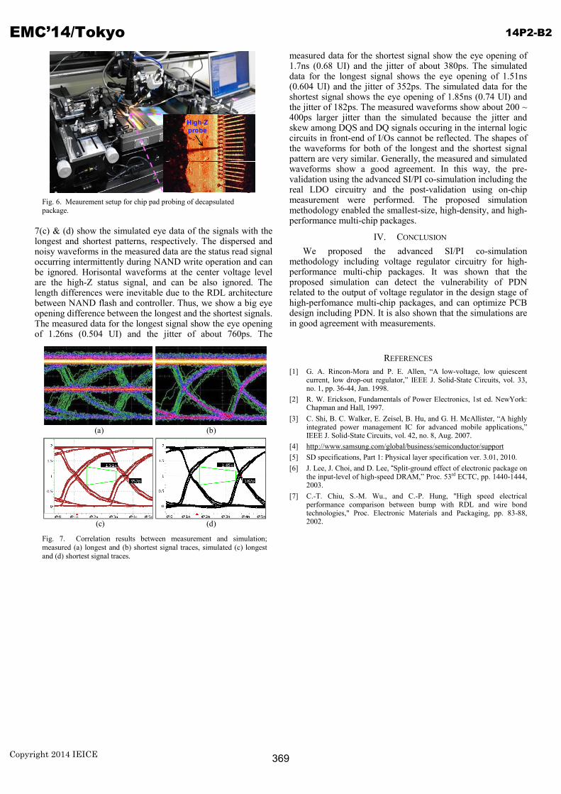
Fig. 6. Meaurement setup for chip pad probing of decapsulated package.
High-Z probe
Fig. 7. Correlation results between measurement and simulation; measured (a) longest and (b) shortest signal traces, simulated (c) longest and (d) shortest signal traces.
(a) (b)
(c) (d)
7(c) & (d) show the simulated eye data of the signals with the longest and shortest patterns, respectively. The dispersed and noisy waveforms in the measured data are the status read signal occurring intermittently during NAND write operation and can be ignored. Horisontal waveforms at the center voltage level are the high-Z status signal, and can be also ignored. The length differences were inevitable due to the RDL architecture between NAND flash and controller. Thus, we show a big eye opening difference between the longest and the shortest signals. The measured data for the longest signal show the eye opening of 1.26ns (0.504 UI) and the jitter of about 760ps. The
measured data for the shortest signal show the eye opening of 1.7ns (0.68 UI) and the jitter of about 380ps. The simulated data for the longest signal shows the eye opening of 1.51ns (0.604 UI) and the jitter of 352ps. The simulated data for the shortest signal shows the eye opening of 1.85ns (0.74 UI) and the jitter of 182ps. The measured waveforms show about 200 ~ 400ps larger jitter than the simulated because the jitter and skew among DQS and DQ signals occuring in the internal logic circuits in front-end of I/Os cannot be reflected. The shapes of the waveforms for both of the longest and the shortest signal pattern are very similar. Generally, the measured and simulated waveforms show a good agreement. In this way, the pre-validation using the advanced SI/PI co-simulation including the real LDO circuitry and the post-validation using on-chip measurement were performed. The proposed simulation methodology enabled the smallest-size, high-density, and high-performance multi-chip packages.
IV. CONCLUSION We proposed the advanced SI/PI co-simulation
methodology including voltage regulator circuitry for high-performance multi-chip packages. It was shown that the proposed simulation can detect the vulnerability of PDN related to the output of voltage regulator in the design stage of high-perfomance multi-chip packages, and can optimize PCB design including PDN. It is also shown that the simulations are in good agreement with measurements.
REFERENCES [1] G. A. Rincon-Mora and P. E. Allen, “A low-voltage, low quiescent
current, low drop-out regulator,” IEEE J. Solid-State Circuits, vol. 33, no. 1, pp. 36-44, Jan. 1998.
[2] R. W. Erickson, Fundamentals of Power Electronics, 1st ed. NewYork: Chapman and Hall, 1997.
[3] C. Shi, B. C. Walker, E. Zeisel, B. Hu, and G. H. McAllister, “A highly integrated power management IC for advanced mobile applications,” IEEE J. Solid-State Circuits, vol. 42, no. 8, Aug. 2007.
[4] http://www.samsung.com/global/business/semiconductor/support [5] SD specifications, Part 1: Physical layer specification ver. 3.01, 2010. [6] J. Lee, J. Choi, and D. Lee, “Split-ground effect of electronic package on
the input-level of high-speed DRAM,” Proc. 53rd ECTC, pp. 1440-1444, 2003.
[7] C.-T. Chiu, S.-M. Wu., and C.-P. Hung, "High speed electrical performance comparison between bump with RDL and wire bond technologies," Proc. Electronic Materials and Packaging, pp. 83-88, 2002.
EMC’14/Tokyo
Copyright 2014 IEICE
14P2-B2
369