1272 ieee transactions on microwave …ecee.colorado.edu/microwave/docs/publications/2007/mtt...1274...
TRANSCRIPT

1272 IEEE TRANSACTIONS ON MICROWAVE THEORY AND TECHNIQUES, VOL. 55, NO. 6, JUNE 2007
Ka-Band Miniaturized Quasi-PlanarHigh-Q Resonators
Kenneth J. Vanhille, Student Member, IEEE, Daniel L. Fontaine, Christopher Nichols, Member, IEEE,Zoya Popovic, Fellow, IEEE, and Dejan S. Filipovic, Member, IEEE
Abstract—Air-filled copper -band resonators with heightsbetween 250–700 m are demonstrated with measured un-loaded factors between 440–829. The low-profile quasi-planarresonators are fabricated using a sequential metal depositionprocess. Miniaturization of up to 70% with respect to a TE101quasi-planar resonator is accomplished by reducing the footprintof the resonator while maintaining the height. Finite-elementsimulations predict the measured resonant frequency within lessthan 1%. Due to fabrication imperfections, un is measured tobe approximately 15% less than predicted. The resonators arecompatible with air-filled rectangular microcoaxial feed linesfabricated in the same metal-deposition process.
Index Terms—Cavity resonator, coaxial transmission line, pho-tolithography, quality ( ) factor.
I. INTRODUCTION
THE miniaturization of microwave resonators, includingreentrant cavity designs, has been of interest since the
development of microwave engineering [1]. Work with filtersusing evanescent waveguide for miniaturization and suppres-sion of spurious modes with the ability to do wideband filtersis presented in [2]. More recently, interest in microfabricatedmicrowave and millimeter-wave resonators using varioustechniques has been seen. The loading of -band surfacemicromachined cavity resonators with barium titanate and alu-mina is examined in [3]; ’s in the hundreds are demonstratedwith fabrication tolerances being the most important limitingfactor on performance. Silicon micromachining of Ku-band res-onators with drain holes used to release the sacrificial materialare fabricated as outlined in [4]; the electrical performance isdecreased by a small amount of leftover silicon in the resonatorafter the processing. Silicon micromachined and metal-platedlayered polymer resonators with miniaturization factors up to70% at - and -bands are presented in [5]. More recently,tuning from 5.4 to 10.9 GHz of an evanescent-mode resonatorwas demonstrated [6]. The resonators presented in [5] and[6] use rib-shaped interdigital capacitor loading (among other
Manuscript received September 29, 2006; revised February 3, 2007.K. J. Vanhille, Z. Popovic, and D. S. Filipovic are with the Department
of Electrical and Computer Engineering, University of Colorado at Boulder,Boulder, CO 80309-0425 USA (e-mail: [email protected];[email protected]; [email protected]).
D. L. Fontaine is with the Advanced Systems and Technology Division, BAESystems, Nashua, NH 03060 USA (e-mail: [email protected]).
C. Nichols is with Rohm and Haas Electronic Materials LLC, Blacksburg,VA 24060 USA (e-mail: [email protected]).
Color versions of one or more of the figures in this paper are available onlineat http://ieeexplore.ieee.org.
Digital Object Identifier 10.1109/TMTT.2007.895232
techniques), and are an excellent starting point for the designspresented here. - and -band rectangular coaxial trans-mission line filters with nickel walls using the electrochemicalfabrication (EFAB) process have been shown in [7] and [8],respectively. In this study, the resonators are not characterizedalone; however, the largest theoretical ’s that can be obtainedfrom nickel coaxial resonators with the same dimensions as in[7] and [8] are less than 80. The same technology with goldplating has recently demonstrated factors near 250 at 60 GHz[9]. Laser etching of copper has been used to fabricate rect-angular coaxial -band filters [10]. 2.5-D resonators usingU-shaped half-wavelength resonators in a cavity operatingin the band have been fabricated using a low-temperatureco-fired ceramic (LTCC) implementation [11]. This methodallows compact filter design by including multiple resonatorsin the same cavity.
Presented here are loaded-cavity resonators fabricatedusing a planarizing sequential-layering process that enablessimultaneous fabrication of integrated rectangular coaxialtransmission lines. Microfabrication of air-filled rectangularcoaxial transmission lines and other components allow highisolation, dense circuit integration, multilayer topologies,low-loss performance, and dominant TEM propagation into the400-GHz range [12]. Rectangular coaxial transmission lines,as well as other air-loaded surface-micromachined passivestructures, such as high-quality factor inductors, have beendemonstrated in the millimeter-wave frequency range [13].Transmission lines, multiport couplers, and bandpass filtershave been fabricated using nickel air-filled coax lines [14].Quasi-planar microfabricated copper branch-line couplers andtransmission-line resonators have been recently presented in[15] with improved electrical properties up to -band.
Results for several quasi-planar resonators fabricated usingthe process presented here are given in [16]. Initial results for aminiaturized quasi-planar resonator are introduced in [17]. Thispaper gives a comprehensive analysis, design, and measurementstudy for miniaturized resonators at different frequencies andwith different loadings. Sensitivity studies of the release holes,new resonator topologies, and behavioral circuit models are pre-sented. Fig. 1(a) shows an example of a miniaturized cavityresonator with an arbitrary loading mechanism. Two types ofpredominately capacitive loading are presented in this paper.Fig. 1(b) shows what we refer to as the “puck-loading” usedat 26 GHz and Fig. 1(c) shows the 36-GHz “rib-loading” struc-ture, described in detail in Section II.
It is worth clarifying the meaning of “quasi-planar” in thecontext of this study. Fig. 2 shows simulated values of for a
0018-9480/$25.00 © 2007 IEEE

VANHILLE et al.: -BAND MINIATURIZED QUASI-PLANAR HIGH- RESONATORS 1273
Fig. 1. (a) Sketch of a loaded quasi-planar resonator showing the loading, rel-evant dimensions, and resonator features. (b) Sketch of the metal puck loadingin the 26-GHz resonator. The four support posts are also shown. (c) Half-viewsketch of the ribs in the 36-GHz loaded cavity resonator. The ribs are cut alongthe xy-plane to simplify their presentation. The relevant dimensions of the res-onators are given in Table I.
Fig. 2. Percentage of Q of a resonator with respect to the maximum Q ofaTE metallic resonator as a function of normalized cavity height h =w forseveral metals. The measured Q values for 26- and 36-GHz fabricated cavityresonators are given.
square cavity with a footprint on the side, and withdifferent metal conductivity values. The height of the cavity ( )is varied from a small value to . The measured unloadedfactors for two unloaded quasi-planar cavity resonators are in-dicated in Fig. 2 for comparison. The normalized heights of thetwo cavities are and , justifying the terminology“quasi planar.” “Low profile” describes these resonators withregard to their height equally well. The small electrical height
Fig. 3. Basic fabrication steps for miniaturized quasi-planar resonators. Thefirst eight steps (S1–S8) are identical for the five- and ten-layer structures.
allows resonators and microcoaxial feeds to be fabricated in thesame process, while simultaneously providing factors higherthan those of coaxial transmission line resonators of the sameheight.
This paper is organized as follows.• Section II details the design of the resonators. Brief de-
scriptions of the fabrication process, and the resonatorfeeding and probing structures are also given.
• Section III provides a portion of the analysis necessary tounderstand the various design parameter effects on the per-formance of the resonators.
• Section IV describes a method for deriving a behavioralcircuit model of the loaded cavity resonators.
• Section V shows the measurement results for the designedresonators.
• Section VI discusses a few final points and indicates po-tential directions for future research.
II. FABRICATION-DRIVEN ANALYSIS AND DESIGN
The PolyStrata process developed by Rohm and Haas Elec-tronic Materials LCC, Blacksburg, VA, consists of sequentiallydepositing layers of metal and photoresist with high aspect ra-tios (2 : 1) [18]. The resonators are fabricated on a low-resis-tivity silicon substrate using a sequence of standard photolitho-graphic steps, as depicted in Fig. 3. Each copper layer is chem-ically polished before the next layer is deposited. The final stepinvolves removing the photoresist, leaving microfabricated air-filled copper structures.
Devices with up to ten layers are demonstrated in this paper.The fabrication and resulting mechanical parameters dictate theelectrical design. The major fabrication-related factors and theirinfluence on component design are as follows.
1) Total resonator height is limited by the number of layersand thickness of each layer. In our case, with ten layers, amaximal cavity height of 700 m is possible, which willlimit the factor as presented in Fig. 2. The electricalheight of the tallest resonator presented in this paper is onetwelfth of a free-space (TEM) wavelength.

1274 IEEE TRANSACTIONS ON MICROWAVE THEORY AND TECHNIQUES, VOL. 55, NO. 6, JUNE 2007
Fig. 4. (a) Puck-loaded cavity resonator taken from [17]. The ports are indi-cated by P1 and P2. The release hole size is 200 � 200 �m. (b) Two cavityresonators fabricated for operation at 36 GHz. The resonator at left (R1) is fullsized, and the resonator at right (R2) uses miniaturization. The release hole sizeis 400� 400 �m. Probing of the structure is done on the ends of the resonator atports indicated by P1 and P2. The loading region in each resonator is indicatedby the dashed lines.
2) Photoresist release holes on the top wall and on the side-walls limit the factor. However, a relatively large numberof holes are required to completely evacuate the lossy di-electric from the cavity. The size and number of releaseholes were carefully examined within fabrication parame-ters and are described in Section II-A.
3) The design of the loading to reduce the size of the res-onator is limited to what can be fabricated with this tech-nology. The main limitation was the size of the loadingstructure, which needed to be mechanically fixed to thetop wall while providing enough loading. We could not usepreviously published designs, as given the mechanical con-straints, they would not provide a sufficiently large loadingreactance. This constraint resulted in a 3-D capacitance,which is unique to this paper and differs from the fins pre-sented in [5].
4) The aspect ratio of a thin cavity is such that the top wall cansag or bulge. The mechanical support posts, which increasethe footprint of the 26-GHz loaded cavity, are eliminatedin the 36-GHz design because of the miniaturization withthe 3-D loading.
5) The inductive coupling between the input -coaxial cableand cavity is constrained by the height of the center con-ductor and the required impedance match; the analysis isdetailed in Section II-C.
Results from two sets of wafers are given in order to show thefabrication constraints on the resonator factor, i.e., 1) a waferwith coaxial components fabricated in a five-layer process withdesign frequencies near 26 GHz and 2) a wafer with 36-GHzcomponents made using a ten-layer process. Resonators fromthe two wafers are shown in Fig. 4.
Fig. 5. NormalizedQ for different sized release holes on a cavity resonator.The surface area of the release holes is kept constant with respect to the topsurface area of the cavity. This is shown for the 250-�m-tall cavities at 26 GHzand 700-�m-tall cavities at 36 GHz.
A. Design of Release Holes
In order to remove lossy photoresist after the top metal layeris deposited, release holes in the top layer and on the sidewallsare necessary. Electrically, these holes perturb the current flowand, therefore, affect the resonant frequency, as well as thefactor. While no holes or small holes will give the highestfactor, many larger holes are needed for high fabrication yield,thus an optimization study is required. The release holes on thesides of these resonators do not have a large effect on the elec-trical performance because of the cavity heights used so onlythe effects of the top holes will be examined. Fig. 5 shows theresults of a 3-D finite-element method (FEM) study, using theAnsoft High Frequency Structure Simulator (HFSS) version 10,of of a cavity resonator versus the number of rows of holeson the cavity resonator top surface (total holes ). Theratio of the surface area of the release holes to the total top-wallsurface area of the resonator is kept constant. For what is fab-ricated, this ratio is 8.74% for the five-layer 26-GHz designs(250- m cavity height) and 21.80% for the ten-layer 36-GHzdesigns (700- m cavity height). These numbers are dictatedby the use of 200 200 m square release holes at 26 GHz
and 400 400 m square release holes at 36 GHz. Fig. 5 shows curves obtained numerically for both
ratios at both design frequencies. The resonant frequency of theresonators changes slightly as the number of holes increases. Tocompare these changes in for a fixed frequency, it is neces-sary to normalize the values.
We begin with the formula for due to the conductor lossesof a rectangular metallic cavity resonator, as can be foundin [19]
(1)
where is the wavenumber, is the wave impedance of thecavity-filling medium, and is the surface resistance of thecavity walls. The length, width, and height of the cavity are ,

VANHILLE et al.: -BAND MINIATURIZED QUASI-PLANAR HIGH- RESONATORS 1275
TABLE IDESIGN VALUES FOR THE PARAMETERS AS NOTED IN FIG. 1
, and , respectively. We assume that and are equal and thatthe cavity is air filled as follows:
(2)
To compare two resonators with the same size, but differentconfigurations of release holes, it is necessary to normalize thecalculated unloaded quality factors based on the frequency ofresonance. If the cavity dimensions and materials do not change,we find the ratio of quality factors to be related to a power of theratio of the resonant frequencies
(3)
The data shown in Fig. 5 are simulated for two frequenciesand two top plate surface area to release hole surface area ratiosusing the normalization in (3). The cavity is 250- m tall forthe 26-GHz resonator and 700- m tall for the 36-GHz resonator.We see that the resonator performance is minimally affected bythe release hole size when the cavity is 250- m tall; however,the unloaded of the cavity is large enough in the 700- m-tallcase in that an effect on the is seen for large hole sizes.
B. Mechanical Support
The values of the dimensions labeled in Fig. 1 are given inTable I. The puck-loaded cavity contains four mechanical sup-port posts that connect the top and bottom cavity walls. Theadded mechanical strength comes with a penalty in size, as theposts behave as inductances in parallel, decreasing the overallinductance of the cavity and increasing the necessary cavityfootprint for a given frequency [17]. The metal rib loaded cavitycontains two ribs connected to the bottom cavity wall and asingle rib hangs from the top cavity wall. A cross configurationis used with the ribs to increase the strength of the connection ofthe ribs to the top and bottom cavity walls. The ribs have the ef-fect of increasing the capacitance of the cavity, operating muchlike an interdigitated capacitor. The rib widths that are not ex-plicitly labeled in Fig. 1(c) are 100 m in size.
C. Coupling
The resonators are measured in a two-port topology withprobing structures in the regions marked P1 and P2 in Fig. 4.150- m-pitch ground–signal–ground (GSG) probes are placedin contact with a short section of vertical rectangular coax, asshown in the figure, where the relatively complex geometry
Fig. 6. (a) Top-view photograph of the probing area for the 36-GHz resonator.(b) Cross-sectional view of the port area (courtesy of the Mayo Foundation).(c) 3-D model of the resonator feed.
serves for impedance matching by reactively tuning the dis-continuity parasitics. The center conductor of the rectangularcoax in the probing region bends downwards to connect to thebottom wall of the cavity, resulting in inductive coupling, asshown in Fig. 1(a). A top view of one of the probe structuresof the 36-GHz resonator is shown in Fig. 6(a). A wafer is diceddown the center line of the rib-loaded resonators to reveal thecross-sectional view shown in Fig. 6(b), giving the sidewallprofiles. An indication of the detailed analysis involved inproducing high-quality transitions to the on-wafer environmentis shown in Fig. 6(c), which gives the computer-aided design(CAD) model of the resonator probe port.
III. RESONATOR MINIATURIZATION
Comprehensive numerical studies are conducted to examinethe effects of several of the design parameters that affect theresonator performance. The more efficient eigenmode analysisis applied to examine parameter effects and trends, while thedriven analysis provides frequency-dependent -parameters.The loading effect of the capacitive puck and the more complex3-D metallic ribs is addressed here.
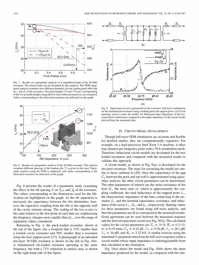
Fig. 7 shows the results of a numerical study of the size ofthe capacitive loading puck of the 26-GHz resonator for puckheights of 75 m and 175 m, corresponding to the two pos-sible values using the five-layer process. The position and sizeof the support posts and the overall dimensions of the resonatorare kept constant. The fabrication process allows three possiblediscrete heights (0, 75, and 175 m), as there are three layersthat make up the actual cavity (two more layers exist, one forthe top wall and one for the bottom wall, making a total of fivelayers). The tallest height is chosen to maximize the factor,whose theoretical value is less than 2% lower than the highestideal value for a copper resonator without release holes.
1276 IEEE TRANSACTIONS ON MICROWAVE THEORY AND TECHNIQUES, VOL. 55, NO. 6, JUNE 2007
Fig. 7. Results of a parametric analysis of a simplified model of the 26-GHzresonator. The release holes are not included for this analysis. The FEM eigen-mode analysis examines how different diameters for the loading puck affect theQ and f of the resonator. Two puck heights (75 and 175 �m) correspondingto the two possible heights using the five-layer fabrication process are examined.Values corresponding to the fabricated resonator are indicated on the graph.
Fig. 8. Results of a parametric analysis of the 36-GHz resonator. The analysisexamines different spacings of the loading ribs S, as given in the inset. Eigen-mode analysis using the FEM is employed, and values corresponding to thefabricated resonator are indicated on the graph.
Fig. 8 presents the results of a parametric study examiningthe effect of the rib spacing on and of the resonator.The values corresponding to the dimensions used for the fab-rication are highlighted on the graph. As the rib separation isincreased, the capacitance between the ribs diminishes; how-ever, the capacitive coupling from the ribs to the opposite wallof the cavity remains strong. The scaling of the two -axes isthe same relative to the first point of each data set, emphasizingthe frequency changes more rapidly than over the range ofseparation values considered.
Returning to Fig. 4, the puck-loaded resonator, shown atthe top of the figure, has a footprint that is 15% smaller thana normal cavity resonator and 50% smaller than a resonatorusing the four support posts [17]. A photograph of an unloadedten-layer 36-GHz resonator is shown on the left in Fig. 4(b).A miniaturized rib-loaded resonator operating at the samefrequency, but with a 71% reduction in surface area, is shownon the right-hand side of this figure.
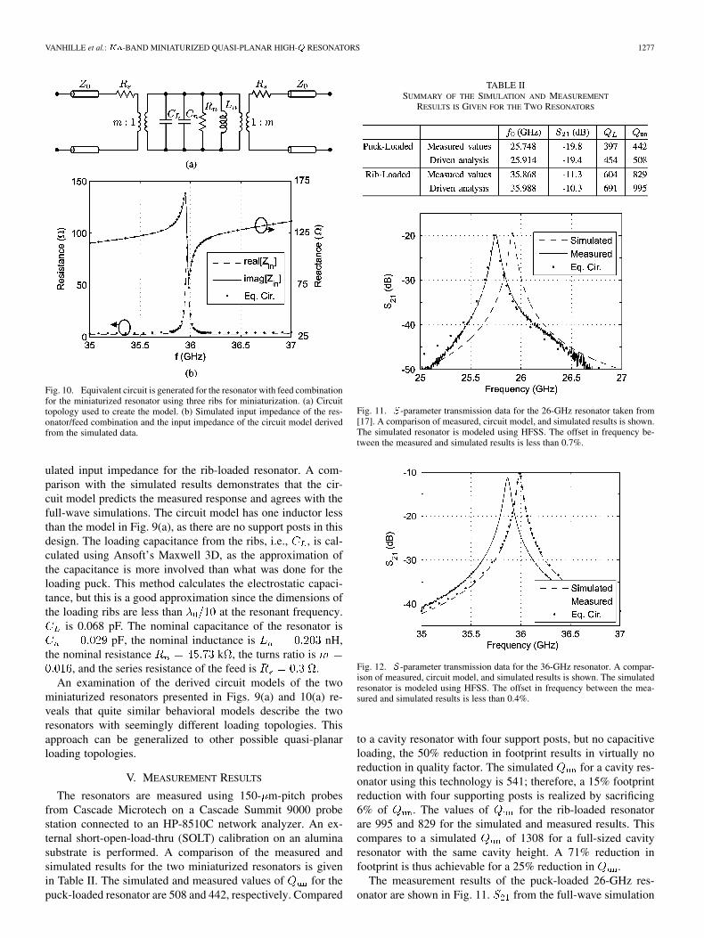
Fig. 9. Equivalent circuit is generated for the resonator with feed combinationfor the miniaturized resonator using a loading puck and support posts. (a) Circuittopology used to create the model. (b) Measured input impedance of the res-onator/feed combination compared to the input impedance of the circuit modelderived from the measured data.
IV. CIRCUIT-MODEL DEVELOPMENT
Though full-wave FEM simulations are accurate and flexiblefor detailed studies, they are computationally expensive. Forexample, on a dual-processor Intel Xeon 3.4 machine, it takesfour minutes per frequency point with a 70-k tetrahedron mesh.Therefore, behavioral circuit models are developed for the twoloaded resonators and compared with the measured results tovalidate this approach.
A circuit model, as shown in Fig. 9(a), is developed for thetwo-port resonator. The steps for extracting the model are sim-ilar to those outlined in [20]. Once the capacitance of the gap
between the puck and top wall is approximated using quasi-static analysis, the other circuit parameters can be determined.The other parameters of interest are the series resistance of thefeed , the turns ratio , which is approximately the cou-pling coefficient, the total inductance of the support posts ,the characteristic impedance of the lines connecting to the res-onator , and the nominal capacitance, resistance, and induc-tance of the cavity , , and , respectively. Starting valuesfor these parameters are found using full-wave analysis, andthen the parameters are fit to correspond to the measured results.Good agreement can be seen between the measured responseand the derived equivalent circuit [see Fig. 9(b)]. The calculatedvalues for the circuit parameters are , ,
turns, pF, pF, pH,pH, and k . A similar exercise using the
simulated -parameter data from the full-wave response yields acircuit model whose input impedance is indistinguishable fromthat calculated in the simulation.
Fig. 10(a) shows the model and Fig. 10(b) shows the inputimpedance predicted by the model, as compared with the sim-
VANHILLE et al.: -BAND MINIATURIZED QUASI-PLANAR HIGH- RESONATORS 1277
Fig. 10. Equivalent circuit is generated for the resonator with feed combinationfor the miniaturized resonator using three ribs for miniaturization. (a) Circuittopology used to create the model. (b) Simulated input impedance of the res-onator/feed combination and the input impedance of the circuit model derivedfrom the simulated data.
ulated input impedance for the rib-loaded resonator. A com-parison with the simulated results demonstrates that the cir-cuit model predicts the measured response and agrees with thefull-wave simulations. The circuit model has one inductor lessthan the model in Fig. 9(a), as there are no support posts in thisdesign. The loading capacitance from the ribs, i.e., , is cal-culated using Ansoft’s Maxwell 3D, as the approximation ofthe capacitance is more involved than what was done for theloading puck. This method calculates the electrostatic capaci-tance, but this is a good approximation since the dimensions ofthe loading ribs are less than at the resonant frequency.
is 0.068 pF. The nominal capacitance of the resonator ispF, the nominal inductance is nH,
the nominal resistance k , the turns ratio is, and the series resistance of the feed is .
An examination of the derived circuit models of the twominiaturized resonators presented in Figs. 9(a) and 10(a) re-veals that quite similar behavioral models describe the tworesonators with seemingly different loading topologies. Thisapproach can be generalized to other possible quasi-planarloading topologies.
V. MEASUREMENT RESULTS
The resonators are measured using 150- m-pitch probesfrom Cascade Microtech on a Cascade Summit 9000 probestation connected to an HP-8510C network analyzer. An ex-ternal short-open-load-thru (SOLT) calibration on an aluminasubstrate is performed. A comparison of the measured andsimulated results for the two miniaturized resonators is givenin Table II. The simulated and measured values of for thepuck-loaded resonator are 508 and 442, respectively. Compared
TABLE IISUMMARY OF THE SIMULATION AND MEASUREMENT
RESULTS IS GIVEN FOR THE TWO RESONATORS
Fig. 11. S-parameter transmission data for the 26-GHz resonator taken from[17]. A comparison of measured, circuit model, and simulated results is shown.The simulated resonator is modeled using HFSS. The offset in frequency be-tween the measured and simulated results is less than 0.7%.
Fig. 12. S-parameter transmission data for the 36-GHz resonator. A compar-ison of measured, circuit model, and simulated results is shown. The simulatedresonator is modeled using HFSS. The offset in frequency between the mea-sured and simulated results is less than 0.4%.
to a cavity resonator with four support posts, but no capacitiveloading, the 50% reduction in footprint results in virtually noreduction in quality factor. The simulated for a cavity res-onator using this technology is 541; therefore, a 15% footprintreduction with four supporting posts is realized by sacrificing6% of . The values of for the rib-loaded resonatorare 995 and 829 for the simulated and measured results. Thiscompares to a simulated of 1308 for a full-sized cavityresonator with the same cavity height. A 71% reduction infootprint is thus achievable for a 25% reduction in .
The measurement results of the puck-loaded 26-GHz res-onator are shown in Fig. 11. from the full-wave simulation

1278 IEEE TRANSACTIONS ON MICROWAVE THEORY AND TECHNIQUES, VOL. 55, NO. 6, JUNE 2007
and the equivalent-circuit model of Fig. 9(a) are also plottedfor comparison. The resonant frequency of the measured res-onator differs by less than 0.7% from the predicted value. Themeasurement results of for the rib-loaded 36-GHz resonatorare given in Fig. 12. Again, a comparison is made between thefull-wave simulation and the derived equivalent-circuit model;the deviation of the measured from predicted resonant frequencyis less than 0.4%.
VI. CONCLUSION
Results from two miniaturized resonators have been presentedand their performance and size has been compared to that offull-sized cavity resonators operating at the same frequencies.The puck-loaded resonator achieves a 15% miniaturization inthe footprint of the resonator, while including mechanical sup-porting posts (this gives a 50% reduction in footprint compared toa cavity with just the support posts). The rib-loaded resonator hasa 71% miniaturization in the cavity footprint compared to a stan-dard resonator. The electrical effects of release holes andtheir size and placement are studied. The electrical phenomenaresulting in the miniaturization of the resonators are exploredand the quality factors and cavity footprints are compared tostandard cavity resonators. Behavioral equivalent circuits arederived and their usefulness validated by measurements. Fromhere, one could develop filters, using the circuit models as thebuilding blocks for rapid synthesis. Such resonators can alsobe integrated with rectangular coaxial lines and active elementsfor circuits that require high- factors such as low phase-noiseoscillators and frequency diplexers.
ACKNOWLEDGMENT
The authors would like to thank G. Potvin, BAE systems,Nashua, NH, D. Sherrer and the Rohm and Haas Microfabri-cation Team, Blacksburg, VA, W. Wilkins and her measure-ment team, Mayo Clinic, Rochester, MN, Dr. J. Evans, DefenseAdvanced Research Projects Agency (DARPA), Arlington, VA,and E. Adler, Army Research Laboratory (ARL), Adelphi, MD,for their support. The authors would also like to thank M. Lukic,and Dr. S. Rondineau, both with the University of Colorado atBoulder, for helpful technical input.
REFERENCES
[1] G. L. Ragan, Ed., Microwave Transmission Circuits, ser. MIT Radiat.Lab. New York: McGraw-Hill, 1948, vol. 9.
[2] R. V. Snyder, “New application of evanescent mode waveguide to filterdesign,” IEEE Trans. Microw. Theory Tech., vol. MTT-25, no. 12, pp.1013–1021, Dec. 1977.
[3] C. A. Tavernier, R. M. Henderson, and J. Papapolymerou, “A reduced-size silicon micromachined high-Q resonator at 5.7 GHz,” IEEE Trans.Microw. Theory Tech, vol. 50, no. 10, pp. 2305–2314, Oct. 2002.
[4] K. Strohm, F. Schmuckle, O. Yaglioglu, J.-F. Luy, and W. Heinrich,“3D silicon micromachined RF resonators,” in IEEE MTT-S Int. Mi-crow. Symp. Dig, Philadelphia, PA, Jun. 2003, pp. 1801–1804.
[5] A. Margomenos, B. Liu, S. Hajela, L. Katehi, and W. Chappell, “Pre-cision fabrication techniques and analysis on high-Q evanescent-moderesonators and filters of different geometries,” IEEE Trans. Microw.Theory Tech, vol. 52, no. 11, pp. 2557–2566, Nov. 2004.
[6] S. Hajela, X. Gong, and W. J. Chappell, “Widely tunable high-Qevanescent-mode resonators using flexible polymer substrates,” inIEEE MTT-S Int. Microw. Symp. Dig, Long Beach, CA, Jun. 2005, pp.2139–2142.
[7] R. Chen, E. Brown, and C. Bang, “A compact low-lossKa-band filterusing 3-D micromachined integrated coax,” in Proc. IEEE Int. MEMSConf., Maastricht, The Netherlands, Jan. 2004, pp. 801–804.
[8] J. Reid and R. Webster, “A compact integratedV -band bandpass filter,”in Proc. IEEE AP-S Int. Symp., Monterey, CA, Jul. 2004, pp. 990–993.
[9] E. D. Marsh, J. Reid, and V. S. Vasilyev, “Gold-plated micromachinedmillimeter-wave resonators based on rectangular coaxial transmissionlines,” IEEE Trans. Microw. Theory Tech, vol. 55, no. 1, pp. 78–84, Jan.2007.
[10] I. Llamas-Garro, M. Lancaster, and P. Hall, “Air-filled square coaxialtransmission line and its use in microwave filters,” Proc. Inst. Elect.Eng.—Microw. Antennas Propag., vol. 152, pp. 155–159, Jun. 2005.
[11] L. Rigaudeau, P. Ferrand, D. Baillargeat, S. Bila, S. Verdeyme, M.Lahti, and T. Jaakola, “LTCC 3-D resonators applied to the design ofvery compact filters for Q-band applications,” IEEE Trans. Microw.Theory Tech, vol. 54, no. 6, pp. 2620–2627, Jun. 2006.
[12] M. Lukic, S. Rondineau, Z. Popovic, and D. Filipovic, “Modeling of re-alistic rectangular � -coaxial lines,” IEEE Trans. Microw. Theory Tech,vol. 54, no. 5, pp. 2068–2076, May 2006.
[13] I. Jeong, S.-H. Shin, J.-H. Go, J.-S. Lee, and C.-M. Nam, “High-per-formance air-gap transmission lines and inductors for millimeter-waveapplications,” IEEE Trans. Microw. Theory Tech, vol. 50, no. 12, pp.2850–2855, Dec. 2002.
[14] J. Reid, E. D. Marsh, and R. T. Webster, “Micromachined rectangularcoaxial transmission lines,” IEEE Trans. Microw. Theory Tech, vol. 54,no. 8, pp. 3433–3442, Aug. 2006.
[15] D. S. Filipovic, Z. Popovic, K. Vanhille, M. Lukic, S. Rondineau,M. Buck, G. Potvin, D. Fontaine, C. Nichols, D. Sherrer, S. Zhou,W. Houck, D. Fleming, E. Daniel, W. Wilkins, V. Sokolov, and J.Evans, “Modeling, design, fabrication, and performance of rectangular�-coaxial lines and components,” in IEEE MTT-S Int. Microw. Symp.Dig, San Francisco, CA, Jun. 2006, pp. 1393–1396.
[16] K. J. Vanhille, D. L. Fontaine, C. Nichols, D. S. Filipovic, and Z.Popovic, “Quasi-planar high-Q millimeter-wave resonators,” IEEETrans. Microw. Theory Tech, vol. 54, no. 6, pp. 2439–2446, Jun. 2006.
[17] ——, “A capacitively-loaded quasi-planar Ka-band resonator,” inProc. 36th Eur. Microw. Conf., Manchester, U.K., Sep. 2006, pp.495–497.
[18] D. Sherrer and J. Fisher, “Coaxial waveguide microstructures and themethod of formation thereof,” U.S. Patent 7 012 489, Mar. 14, 2006.
[19] D. Pozar, Microwave Engineering, 2nd ed. New York: Wiley, 1998,pp. 300–350.
[20] F. Gardiol, Introduction to Microwaves. Norwood, MA: ArtechHouse, 1983, pp. 136–142.
Kenneth J. Vanhille (S’00) received the B.S. degreein electrical engineering from Utah State University,Logan, in 2002, the M.S.E.E. degree from the Univer-sity of Colorado at Boulder, in 2005, and is currentlyworking toward the Ph.D. degree at the University ofColorado at Boulder.
From 2000 to 2003, he was with the SpaceDynamics Laboratory, Logan, UT, where he de-signed space science instrumentation for soundingrocket campaigns. In 2002, he was a member ofthe National Aeronautics and Space Administration
(NASA) Academy, Goddard Space Flight Center. His current interests includemillimeter-wave components and antenna design.
Daniel L. Fontaine was born in Holyoke, MA, onFebruary 17, 1966. He received the B.S. and M.S.degrees in electrical engineering from the Universityof Massachusetts at Amherst, in 1988 and 1991,respectively.
From 1988 to 1996, he was a Senior Design Engi-neer with the Raytheon Company, Tewksbury, MA.Since 1996, he has been a Principal Design Engineerwith the Advanced Systems and Technology Divi-sion, BAE Systems, Nashua, NH. His professionaldesign experience and interests include microwave
and millimeter-wave patch antennas and arrays, quasi-optical feed networks,transmit/receive (T/R) modules, and frequency-selective surfaces.

VANHILLE et al.: -BAND MINIATURIZED QUASI-PLANAR HIGH- RESONATORS 1279
Christopher Nichols (M’03) received the B.S. de-gree in physics from Arkansas State University, StateUniversity, in 1990, and the M.S. degree in physicsand Ph.D. degree in applied science from The Col-lege of William and Mary, Williamsburg, VA, in 1992and 1996, respectively. His doctoral dissertation in-volved the engineering of a novel hyperthermal neu-tral stream etch process tool for charge-free waferstripping.
Prior to graduation, he was with IBM, YorktownHeights, NY, where he was involved with ionized
physical vapor deposition. He is currently a Senior Engineer and Microfab-rication Program Manager with Rohm and Haas Electronic Materials LLC,Blacksburg, VA.
Zoya Popovic (S’86–M’90–SM’99–F’02) receivedthe Dipl.Ing. degree from the University of Belgrade,Belgrade, Serbia, in 1985, and the Ph.D. degree fromthe California Institute of Technology, in 1990.
She is currently the Hudson Moore Jr. Chaired Pro-fessor of Electrical and Computer Engineering withthe University of Colorado at Boulder. Her researchinterests include high-efficiency and low-noise mi-crowave circuits, quasi-optical millimeter-wave tech-niques, smart and multibeam antenna arrays, intelli-gent RF front ends, RF optics, and wireless powering
for batteryless sensors.
Dr. Popovic was the recipient of the 1993 and 2006 IEEE Microwave Theoryand Techniques Society (IEEE MTT-S) Microwave Prize for best journal pa-pers. She was also the recipient of the 1996 URSI Issac Koga Gold Medal, a2000 Humboldt Research Award for Senior U.S. Scientists, and a 1993 NationalScience Foundation (NSF) Presidential Faculty Fellow Award.
Dejan S. Filipovic (S’97–M’02) received the Dipl.Eng. degree in electrical engineering from the Uni-versity of Nis, Nis, Serbia, in 1994, and the M.S.E.E.and Ph.D. degrees from The University of Michiganat Ann Arbor, in 1999 and 2002, respectively.
From 1994 to 1997, he was a Research Assistantwith the University of Nis. From 1997 to 2002,he was a Graduate Student with the University ofMichigan at Ann Arbor. He is currently an AssistantProfessor with the University of Colorado at Boulder.His research interests are in the development of
millimeter-wave components and systems, multiphysics modeling, antennatheory and design, as well as in computational and applied electromagnetics.