1/1301 general specification - power modules
TRANSCRIPT
1/1301 GENERAL SPECIFICATION 1 (4)
Prepared (also subject responsible if other) No.
EZHIXZH Kevin Zhou E 1/1301-BMR4580011 Uen Approved Checked Date Rev Reference
2020-04-24 PA1
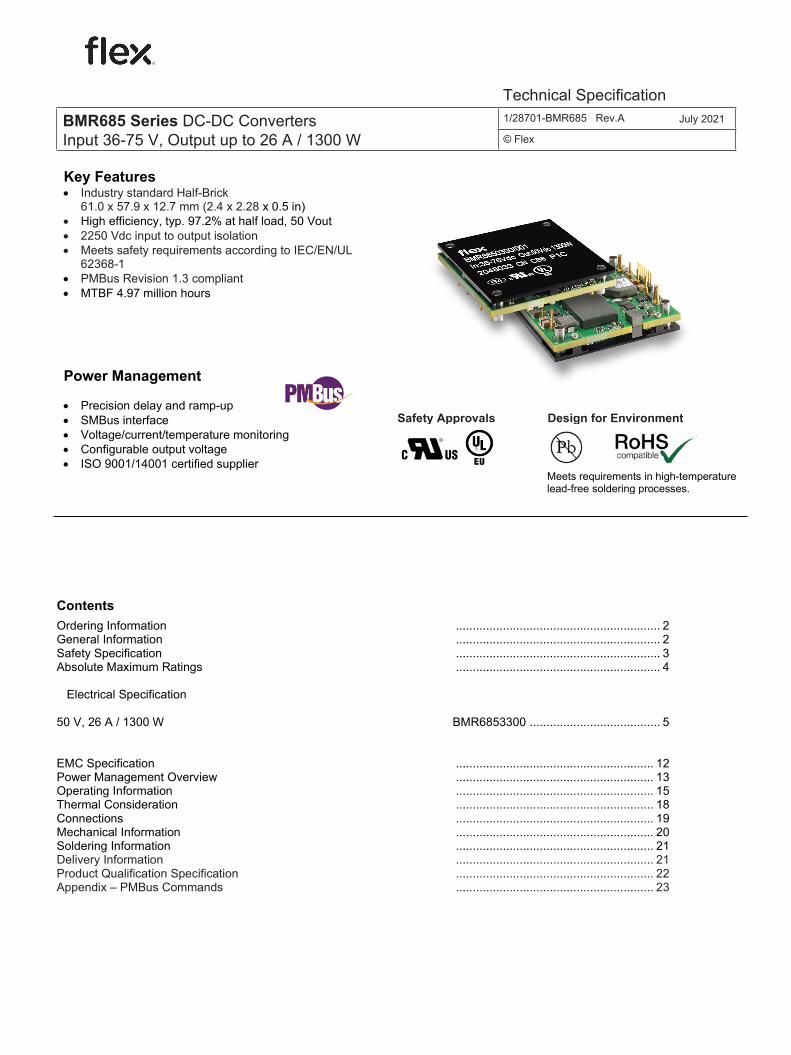
Key Features • Industry standard Half-Brick
61.0 x 57.9 x 12.7 mm (2.4 x 2.28 x 0.5 in)• High efficiency, typ. 97.2% at half load, 50 Vout• 2250 Vdc input to output isolation• Meets safety requirements according to IEC/EN/UL
62368-1• PMBus Revision 1.3 compliant• MTBF 4.97 million hours
Power Management
• Precision delay and ramp-up• SMBus interface• Voltage/current/temperature monitoring• Configurable output voltage• ISO 9001/14001 certified supplier
Safety Approvals Design for Environment
Meets requirements in high-temperature lead-free soldering processes.
Ericsson Internal TABLE OF CONTENTS 1 (1)
Prepared (also subject responsible if other) No.
Kevin Zhou Approved Checked Date Rev Reference
Kevin Zhou 2017-09-28 B
Contents Ordering Information ............................................................. 2 General Information ............................................................. 2 Safety Specification ............................................................. 3 Absolute Maximum Ratings ............................................................. 4
Electrical Specification
50 V, 26 A / 1300 W BMR6853300 ....................................... 5
EMC Specification ........................................................... 12 Power Management Overview ........................................................... 13 Operating Information ........................................................... 15 Thermal Consideration ........................................................... 18 Connections ........................................................... 19 Mechanical Information ........................................................... 20 Soldering Information ........................................................... 21 Delivery Information ........................................................... 21 Product Qualification Specification ........................................................... 22 Appendix – PMBus Commands ........................................................... 23
BMR685 Series DC-DC Converters Input 36-75 V, Output up to 26 A / 1300 W
1/28701-BMR685 Rev.A July 2021
© Flex
Technical Specification
1/1301 GENERAL SPECIFICATION 2 (4)
Prepared (also subject responsible if other) No.
EZHIXZH Kevin Zhou E 1/1301-BMR4580011 Uen Approved Checked Date Rev Reference
2020-04-24 PA1
Ordering Information Product program Vin Output BMR685x3xx/xxx 36 - 75 50 V / 26 A, 1300 W
Product number and Packaging BMR685 n1 n2 n3 n4 / n5 n6 n7 n8 Mechanical pin option x /
Mechanical option x /
Hardware option x x /
Configuration file / x x x
Packaging(optional) / x
Options Description
n1
n2
n3n4
n5 n6 n7
n8
4 = Pin length 2.79 mm 3 = Pin length 4.57 mm 2 = Pin length 3.69 mm
3 = Baseplate
00 = 36-75 Vin, 50 Vout, DOSA 7 pin digital interface 01 = 36-75 Vin, 50 Vout, without digital interface
001 = 50 V standard configuration N logic 002 = 50 V standard configuration P logic
Blank = 30 converters (through hole pin)/tray, 3 trays/box, PE foam dissipative
Example: Product number BMR6853300/001 equals a through hole mount pin length 4.57 mm, baseplate, digital interface with 50V standard configuration variant.
For application specific configurations contact your local Flex sales representative.
General Information Reliability The failure rate (λ) and mean time between failures (MTBF= 1/λ) is calculated at max output power and an operating ambient temperature (TA) of +40°C. Flex uses Telcordia SR-332 Issue 4 Method 1 to calculate the mean steady-state failure rate and standard deviation (σ).
Telcordia SR-332 Issue 4 also provides techniques to estimate the upper confidence levels of failure rates based on the mean and standard deviation.
Mean steady-state failure rate, λ
Std. deviation, σ
201 nFailures/h 11 nFailures/h
MTBF (mean value) for the BMR685 series = 4.97 Mh.
MTBF at 90% confidence level = 4.65 Mh
Compatibility with RoHS requirements The products are compatible with the relevant clauses and requirements of the RoHS directive 2011/65/EU and have a maximum concentration value of 0.1% by weight in homogeneous materials for lead, mercury, hexavalent chromium, PBB and PBDE and of 0.01% by weight in homogeneous materials for cadmium.
Exemptions in the RoHS directive utilized in Flex products are found in the Statement of Compliance document.
Flex fulfills and will continuously fulfill all its obligations under regulation (EC) No 1907/2006 concerning the registration, evaluation, authorization and restriction of chemicals (REACH) as they enter into force and is through product materials declarations preparing for the obligations to communicate information on substances in the products.
Quality Statement The products are designed and manufactured in an industrial environment where quality systems and methods like ISO 9000, Six Sigma, and SPC are intensively in use to boost the continuous improvements strategy. Infant mortality or early failures in the products are screened out and they are subjected to an ATE-based final test. Conservative design rules, design reviews and product qualifications, plus the high competence of an engaged work force, contribute to the high quality of the products.
Warranty Warranty period and conditions are defined in Flex General Terms and Conditions of Sale.
Limitation of Liability Flex does not make any other warranties, expressed or implied including any warranty of merchantability or fitness for a particular purpose (including, but not limited to, use in life support applications, where malfunctions of product can cause injury to a person’s health or life).
© Flex 2021 The information and specifications in this technical specification is believed to be correct at the time of publication. However, no liability is accepted for inaccuracies, printing errors or for any consequences thereof. Flex reserves the right to change the contents of this technical specification at any time without prior notice.
BMR685 Series DC-DC Converters Input 36-75 V, Output up to 26 A / 1300 W
1/28701-BMR685 Rev.A July 2021
© Flex
Technical Specification 2
1/1301 GENERAL SPECIFICATION
3 (4) Prepared (also subject responsible if other) No.
EZHIXZH Kevin Zhou E 1/1301-BMR4580011 Uen Approved Checked Date Rev Reference
2020-04-24 PA1
Safety Specification General information Flex DC/DC converters and DC/DC regulators are designed in accordance with the safety standards IEC 62368-1, EN 62368-1 and UL 62368-1 Safety of Information Technology Equipment. IEC/EN/UL 62368-1 contains requirements to prevent injury or damage due to the following hazards:
• Electrical shock • Energy hazards • Fire • Mechanical and heat hazards • Radiation hazards • Chemical hazards
On-board DC/DC converters and DC/DC regulators are defined as component power supplies. As components they cannot fully comply with the provisions of any safety requirements without “conditions of acceptability”. Clearance between conductors and between conductive parts of the component power supply and conductors on the board in the final product must meet the applicable safety requirements. Certain conditions of acceptability apply for component power supplies with limited stand-off (see Mechanical Information and Safety Certificate for further information). It is the responsibility of the installer to ensure that the final product housing these components complies with the requirements of all applicable safety standards and regulations for the final product. Component power supplies for general use should comply with the requirements in IEC/EN/UL 62368-1 Safety of Information Technology Equipment. Product related standards, e.g. IEEE 802.3af Power over Ethernet, and ETS-300132-2 Power interface at the input to telecom equipment, operated by direct current (dc) are based on IEC/EN/UL 62368-1 with regards to safety. Flex DC/DC converters, Power interface modules and DC/DC regulators are UL 62368-1 recognized and certified in accordance with EN 62368-1. The flammability rating for all construction parts of the products meet requirements for V-0 class material according to IEC 60695-11-10, Fire hazard testing, test flames – 50 W horizontal and vertical flame test methods.
The output is considered as safety extra low voltage (SELV) if one of the following conditions is met:
• The input source provides double or reinforced insulation from the AC mains according to IEC/EN/UL 62368-1.
• The input source provides basic or supplementary insulation from the AC mains and the product’s output is reliably connected to protective earth according to IEC/EN/UL 62368-1.
• The input source is reliably connected to protective earth and provides basic or supplementary insulation according to IEC/EN/UL 62368-1 and the maximum input source voltage is 60 Vdc.
Galvanic isolation between input and output is verified in an electric strength test and the isolation voltage (Viso) meets the voltage strength requirement for basic insulation according to IEC/EN/UL 62368-1. It is recommended to use a slow blow fuse at the input of each DC/DC converter. If an input filter is used in the circuit the fuse should be placed in front of the input filter. In the rare event of a component problem that imposes a short circuit on the input source, this fuse will provide the following functions:
• Isolate the fault from the input power source so as not to affect the operation of other parts of the system
• Protect the distribution wiring from excessive current and power loss thus preventing hazardous overheating
BMR685 Series DC-DC Converters Input 36-75 V, Output up to 26 A / 1300 W
1/28701-BMR685 Rev.A July 2021
© Flex
Technical Specification 3

PUBLIC
PRODUCT SPECIFICATION
1 (9) Prepared (Subject resp) No.
JIDIBIBX Li Bo 2/1301-BMR 6850 0000 Uen Approved (Document resp) Checked Date Rev
JIDIBIBX Li Bo 12/14/20201 C Product specificationAbsolute Maximum Ratings
Characteristics min typ max Unit TBP Base plate Operating Temperature -40 +100 °C TP1 Operating Temperature (see Thermal Consideration section) -40 +125 °C TS Storage temperature -55 +125 °C VI Input voltage -0.5 +75 V
Viso Isolation voltage (input to output test voltage) 2250 Vdc Viso Isolation voltage (base plate to output test voltage) 750 Vdc
Vtr Input voltage transient (tp 100 ms) 100 V
VRC Remote Control pin voltage
-0.3 5 V
Stress in excess of Absolute Maximum Ratings may cause permanent damage. Absolute Maximum Ratings, sometimes referred to as no destruction limits, are normally tested with one parameter at a time exceeding the limits in the Electrical Specification. If exposed to stress above these limits, function and performance may degrade in an unspecified manner.
Fundamental Circuit Diagram
BMR685 Series DC-DC Converters Input 36-75 V, Output up to 26 A / 1300 W
1/28701-BMR685 Rev.A July 2021
© Flex
Technical Specification 4

PUBLIC
PRODUCT SPECIFICATION
2 (9) Prepared (Subject resp) No.
JIDIBIBX Li Bo 2/1301-BMR 6850 0000 Uen Approved (Document resp) Checked Date Rev
JIDIBIBX Li Bo 12/14/20201 C Common Electrical Specification This section includes parameter specifications common to all product versions within the product series. Typically, these are parameters defined by the digital controller of the products. In the table below PMBus commands for configurable parameters are written in capital letters. TP1 = -40 to +85 °C, VI = 36 to 75 V, unless otherwise specified under Conditions. Typical values given at: TP1 = +25 °C, VI = 48 V, max IO, unless otherwise specified under Conditions: Characteristics Conditions min typ max Unit
fSW = 1/TSW
Switching Frequency 120 kHz Switching Frequency Set-point Accuracy TP1 = +25 °C -2 2 %
TINIT Initialization Time From VI > ~27 V to ready to be enabled 60 ms
TONdel_tot Output voltage Total On Delay Time
Enable by input voltage TINIT + TONdel Enable by RC or CTRL pin TONdel
TONdel Output voltage On Delay Time
PMBus configurable Turn on delay duration 250 ms
Range TON_DELAY 0 32767 ms
Accuracy (actual delay vs set value) ±5 %
TOFFdel Output voltage Off Delay Time
PMBus configurable Turn off delay duration, Note 2
5 ms
Range TOFF_DELAY 0 32767 ms
Accuracy (actual delay vs set value), Note 3 ±5 %
TONrise / TOFFfall
Output voltage On/Off Ramp Time (0-100%-0 of VO)
Turn on ramp duration -Stand alone
100 ms
Turn off ramp duration 20 ms Range TON_RISE/TOFF_FALL 20 32767 ms
Ramp time accuracy for standalone operation (actual ramp time vs set value) ±5 %
VIoff Input turn off range States the level where the output voltage is disabled, PMBus configurable 31 75 V
VIon Input turn on range States the level where the output voltage is enabled, PMBus configurable. 33 75 V
BMR685 Series DC-DC Converters Input 36-75 V, Output up to 26 A / 1300 W
1/28701-BMR685 Rev.A July 2021
© Flex
Technical Specification 5

PUBLIC
PRODUCT SPECIFICATION
3 (9) Prepared (Subject resp) No.
JIDIBIBX Li Bo 2/1301-BMR 6850 0000 Uen Approved (Document resp) Checked Date Rev
JIDIBIBX Li Bo 12/14/20201 C Characteristics Conditions min typ max Unit
Power Good, PG
PG threshold
PMBus configurable Rising 40 V
PMBus configurable Falling 30 V
PG thresholds range POWER_GOOD_ON VOUT_UV_FAULT_LIMIT 0 100 % VO
PG delay From VO reaching target to PG assertion 1 ms
Input Under Voltage Protection, IUVP
IUVP threshold PMBus configurable 0 V IUVP threshold range VIN_UV_FAULT_LIMIT 0-100 %VIN IUVP hysteresis PMBus configurable 0 V
IUVP hysteresis range VIN_UV_FAULT_LIMIT- VIN_UV_WARN_LIMIT 0 V
Set point accuracy 1 % IUVP response delay 100 μs
Fault response PMBus configurable VIN_UV_FAULT_RESPONSE Ignore fault
Input Over Voltage Protection, IOVP
IOVP threshold PMBus configurable 78 V IOVP threshold range VIN_OV_FAULT_LIMIT 0-100 %VIN
IOVP hysteresis PMBus configurable VIN_OV_FAULT_LIMIT- VIN_OV_WARN_LIMIT
0 V
IOVP hysteresis range VIN_OV_WARN_LIMIT 0-100 %VIN Set point accuracy ±1 % IOVP response delay 100 μs
Fault response PMBus configurable VIN_OV_FAULT_RESPONSE Disable until Fault Cleared
Output Voltage Over/Under Voltage Protection, OVP/UVP
UVP threshold PMBus configurable 0 VO UVP threshold range VOUT_UV_FAULT_LIMIT 0-100 %VO OVP threshold PMBus configurable 59 V OVP threshold range VOUT_OV_FAULT_LIMIT 0-63.999 V
UVP/OVP response time 100/50 μs
Fault response
PMBus configurable VOUT_UV_FAULT_RESPONSE Ignore fault
PMBus configurable VOUT_OV_FAULT_RESPONSE Disable until Fault Cleared
Over Current Protection, OCP Note 5
OCP threshold PMBus configurable 32 A OCP threshold range IOUT_OC_FAULT_LIMIT 0-32 A Protection delay See Note 4 0 ms
Fault response PMBus configurable MFR_IOUT_OC_FAULT_RESPONSE
hiccup
Over Temperature Protection, OTP, Note 6
OTP threshold PMBus configurable 125 °C OTP threshold range OT_FAULT_LIMIT -50 +150 °C
OTP hysteresis PMBus configurable OT_FAULT_LIMIT- OT_WARN_LIMIT 25 °C
Fault response PMBus configurable OT_FAULT_RESPONSE
hiccup
BMR685 Series DC-DC Converters Input 36-75 V, Output up to 26 A / 1300 W
1/28701-BMR685 Rev.A July 2021
© Flex
Technical Specification 6

PUBLIC
PRODUCT SPECIFICATION
4 (9) Prepared (Subject resp) No.
JIDIBIBX Li Bo 2/1301-BMR 6850 0000 Uen Approved (Document resp) Checked Date Rev
JIDIBIBX Li Bo 12/14/20201 C Characteristics Conditions min typ max Unit
Monitoring Accuracy
Input voltage READ_VIN ±500 mV
Output voltage READ_VOUT ±200 mV
Output current READ_IOUT ±0.5 A
Temperature READ_TEMPERATURE_1 Temperature sensor, -30 - 125 °C ±3 °C
VOL Logic output low signal level SCL, SDA, SALERT, PG
Sink / source current = 4 mA Note 7
0.25 V
VOH Logic output high signal level 2.7 V
IOL Logic output low sink current 4 mA IOH Logic output high source current 4 mA VIL Logic input low threshold
SCL, SDA 1.1 V
VIH Logic input high threshold 2.1 V CI_PIN Logic pin input capacitance SCL, SDA 10 pF
fSMB Supported SMBus Operating frequency 100 400 kHz
TBUF SMBus Bus free time STOP bit to START bit See section SMBus – Timing 1.3 µs
tset SMBus SDA setup time from SCL See section SMBus – Timing 100 ns thold SMBus SDA hold time from SCL See section SMBus – Timing 0 ns
SMBus START/STOP condition setup/hold time from SCL 600 ns
Tlow SCL low period 1.3 µs Thigh SCL high period 0.6 50 µs
Note 1. There are configuration changes to consider when changing the switching frequency, see section Switching Frequency. Note 2. A default value of 0 ms forces the device to Immediate Off behavior with TOFF_FALL ramp-down setting being ignored. Note 3. The specified accuracy applies for off delay times larger than 4 ms. When setting 0 ms the actual delay will be 0 ms. Note 4. According to the combination of command MFR_RESPONSE_UNIT_CFG and delay time set in IOUT_OC_FAULT_RESPONSE, see Appendix – PMBus commands. Note 5. Note that higher OCP threshold than specified may result in damage of the module at OC fault conditions. The ocp fault response can be configurable by FPD Note 6. See section Over Temperature Protection (OTP). The OTP fault response can be configurable by FPD. Note 7. SCL, SDA, SALERT, PG have no internal pull up resistor.
BMR685 Series DC-DC Converters Input 36-75 V, Output up to 26 A / 1300 W
1/28701-BMR685 Rev.A July 2021
© Flex
Technical Specification 7

PUBLIC
PRODUCT SPECIFICATION
5 (9) Prepared (Subject resp) No.
JIDIBIBX Li Bo 2/1301-BMR 6850 0000 Uen Approved (Document resp) Checked Date Rev
JIDIBIBX Li Bo 12/14/20201 C
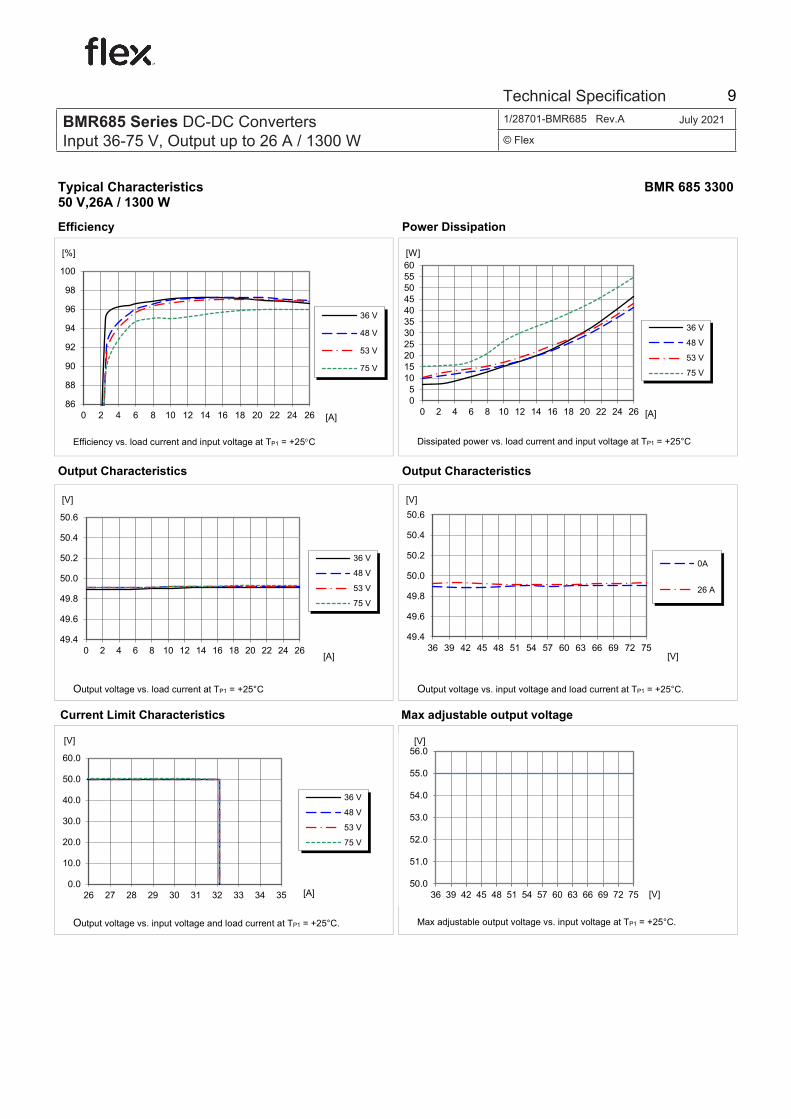
Electrical Specification 50 V, 26A / 1300 W
BMR 685 3300
TP1 = -40 to +85ºC, VI = 36 to 75 V, unless otherwise specified under Conditions. Typical values given at: TP1 = +25°C, VI= 48 V, max PO, unless otherwise specified under Conditions. Additional Cout = 1.64 mF, Cin = 0.47 mF Characteristics Conditions min typ max Unit VI Input voltage range 36 75 V VIoff Turn-off input voltage Decreasing input voltage 31 32 33 V VIon Turn-on input voltage Increasing input voltage 33 34 35 V Ci Internal input capacitance VI = 48 V 24 µF PO Output power Note 1, 2 0 1300 W
η Efficiency 50% of max IO, VI = 48 V 96.5 97.2
% max IO, VI = 48 V 96 97
Pd Power Dissipation max IO 38.5 60 W Pli Input idling power IO = 0 A, VI = 48 V 9.6 W PRC Input standby power VI = 48 V (turned off with RC) 1.2 W fs Switching frequency 0-100% of max PO 120 kHz
VOi Output voltage initial setting and accuracy TP1 = +25°C, VI = 48 V, PO = 0 W 49 50 51 V
VO
Output adjust range 0-100% of max PO, see Note 1 25 55 V Output voltage tolerance band 0-100% of max PO, see Note 1 49 51 V Idling voltage PO = 0 W 49 51 V Line regulation VI = 36 - 75 V, 100% of max PO 100 mV Load regulation VI = 48 V, 0-100% of max PO 200 500 mV
Vtr Load transient voltage deviation
VI = 48 V, Load step 25-75-25% of max IO, di/dt = 1 A/μs. See Note 2
±500 mV
ttr Load transient recovery time 500 µs
tr Ramp-up time (from 0−100% of VOi) 0-100% of max PO
100 ms
ts Start-up time (from VI connection to 100% of VOi) 420 ms
tRC RC start-up time max PO 360 ms
RC Sink current 0.3 mA Trigger level RC-voltage 1.6 V Response time 1 ms
IO Output current VI = 36 – 75 V 0 26 A Ilim Current limit threshold TP1 < max TP1 28 32 34 A Isc Short circuit current TP1 = 25ºC, Irms, see Note 3 1 A Cout Recommended Capacitive Load TP1 = 25ºC,see Note4 820 3300 µF
VOac Output ripple & noise See ripple & noise section, max PO, see Note 5 40 500 mVp-p
OVP Output over voltage protection 59 59.5 V Note 1: Cout = 820 µF, EGPA500EBC821MK30S. Note 2: 3pcs 470µF MPN: UPW2A471MHD. 1pc 220uF UPW2A221MHD, 1pc 15uF 100SXE15M oscon. Note 3: Hiccup short circuit protection; RMS output current is the presented. Note 4: If the ambient temp is less than -25°C, double minimum output capacitance is necessary.
Note 5: Filter 10 µF tantalum + 0.1 µF ceramic.
BMR685 Series DC-DC Converters Input 36-75 V, Output up to 26 A / 1300 W
1/28701-BMR685 Rev.A July 2021
© Flex
Technical Specification 8
PUBLIC
PRODUCT SPECIFICATION
6 (9) Prepared (Subject resp) No.
JIDIBIBX Li Bo 2/1301-BMR 6850 0000 Uen Approved (Document resp) Checked Date Rev
JIDIBIBX Li Bo 12/14/20201 C Typical Characteristics 50 V,26A / 1300 W
BMR 685 3300
Efficiency Power Dissipation
Efficiency vs. load current and input voltage at TP1 = +25°C Dissipated power vs. load current and input voltage at TP1 = +25°C
Output Characteristics Output Characteristics
Output voltage vs. load current at TP1 = +25°C Output voltage vs. input voltage and load current at TP1 = +25°C.
Current Limit Characteristics Max adjustable output voltage
Output voltage vs. input voltage and load current at TP1 = +25°C. Max adjustable output voltage vs. input voltage at TP1 = +25°C.
86
88
90
92
94
96
98
100
0 2 4 6 8 10 12 14 16 18 20 22 24 26
[%]
[A]
36 V
48 V
53 V
75 V
05
1015202530354045505560
0 2 4 6 8 10 12 14 16 18 20 22 24 26
[W]
[A]
36 V
48 V
53 V
75 V
49.4
49.6
49.8
50.0
50.2
50.4
50.6
0 2 4 6 8 10 12 14 16 18 20 22 24 26
[V]
[A]
36 V
48 V
53 V
75 V
49.4
49.6
49.8
50.0
50.2
50.4
50.6
36 39 42 45 48 51 54 57 60 63 66 69 72 75
[V]
[V]
0A
26 A
0.0
10.0
20.0
30.0
40.0
50.0
60.0
26 27 28 29 30 31 32 33 34 35
[V]
[A]
36 V
48 V
53 V
75 V
50.0
51.0
52.0
53.0
54.0
55.0
56.0
36 39 42 45 48 51 54 57 60 63 66 69 72 75
[V]
[V]
BMR685 Series DC-DC Converters Input 36-75 V, Output up to 26 A / 1300 W
1/28701-BMR685 Rev.A July 2021
© Flex
Technical Specification 9

PUBLIC
PRODUCT SPECIFICATION
7 (9) Prepared (Subject resp) No.
JIDIBIBX Li Bo 2/1301-BMR 6850 0000 Uen Approved (Document resp) Checked Date Rev
JIDIBIBX Li Bo 12/14/20201 C
Typical Characteristics 50 V,26A / 1300 W
BMR 685 3300
Start-up Shut-down
Start-up enabled by connecting VI at: TP1 = +25°C, VI = 48 V, IO = 17.9A load.
Top trace: output voltage 20 V/div. Bottom trace: input voltage 20 V/div. Time scale: 100 ms/div
Shut-down enabled by disconnecting VI at: TP1= +25°C, VI = 48 V, IO = 26A load.
Top trace: output voltage 20 V/div. Bottom trace: input voltage 20 V/div. Time scale: 10 ms/div.
Output Ripple & Noise Output Load Transient Response
Output voltage ripple at: TP1= +25°C, VI = 48 V, IO = 26A load.
Trace: output voltage 50 mV/div. Time scale: 5 µs/div. Output voltage response to load current step-
change 6.5-19.5-6.5 A (1 A/µs) at: TP1=+25°C, VI = 48 V. with 3pcs 470µF+1pcs 220uf+1pcs 15uf
Top trace: output voltage 1000 mV/div. Bottom trace: load current 10 A/div. Time scale: 1 ms/div.
Output Voltage Adjust (see operating information) Passive adjust The resistor value for an adjusted output voltage is calculated by using the following equations: Output Voltage Adjust, Decrease:
−
∆= 2
%100Radj k
Output Voltage Adjust, Increase:
( )
−
∆−
∆×∆+×
= 2%
100%225.1
%10050Radj kΩ
Example: Increase 10% => Vo = 55 Vdc
( )
−−
×+× 2
10100
10225.11010050
kΩ = 437 kΩ
Active adjust The output voltage can be adjusted using a voltage applied to the Vadj pin. This voltage is calculated by using the following equation:
𝑉𝑉𝑉𝑉𝑉𝑉𝑉𝑉 = 1.225 + (𝑅𝑅𝑉𝑉𝑉𝑉𝑉𝑉 + 2) × 1.225 ×𝑉𝑉𝑉𝑉𝑉𝑉𝑉𝑉𝑉𝑉𝑉𝑉𝑉𝑉𝑉𝑉 − 50
50
BMR685 Series DC-DC Converters Input 36-75 V, Output up to 26 A / 1300 W
1/28701-BMR685 Rev.A July 2021
© Flex
Technical Specification 10

PUBLIC
PRODUCT SPECIFICATION
8 (9) Prepared (Subject resp) No.
JIDIBIBX Li Bo 2/1301-BMR 6850 0000 Uen Approved (Document resp) Checked Date Rev
JIDIBIBX Li Bo 12/14/20201 C
Typical Characteristics 50 V,26A / 1300 W
BMR 685 3300
Output Current Derating – Cold wall sealed box
Available load current vs Base plate temperature. VI = 48 V. See Thermal Consideration section.
0
5
10
15
20
25
30
0 20 40 60 80 100
[A]
[°C]
Tamb 85°C
BMR685 Series DC-DC Converters Input 36-75 V, Output up to 26 A / 1300 W
1/28701-BMR685 Rev.A July 2021
© Flex
Technical Specification 11

INTERNAL USE ONLY
PRODUCT SPECIFICATION
1 (8) Prepared (Subject resp) No.
JIDIBIBX Li Bo 3/1301-BMR 685 0000Uen Approved (Document resp) Checked Date Rev
JIDIBIBX Li Bo 12/14/20201 B EMC Specification Conducted EMI measured according to EN55022 / EN55032, CISPR 22 / CISPR 32 and FCC part 15J (see test set-up). The fundamental switching frequency is 120 kHz for BMR685. The EMI characteristics below is measured at VI = 48 V and max IO. Optional external filter for class B Suggested external input filter in order to meet class B in EN 55022 / EN 55032, CISPR 22 / CISPR 32 and FCC part 15J.
Filter components: M1, M2: 1mH, Wurth 7448262510 C1,C2,C5,C6: Each of Cx should use 4*4.7uF/100V in parallel C3,C4: Each of Cx should use 5*4.7uf/100V in parallel C7-C20: 220 nF/630V
EMI with filter, EN55032 Test method and limits are the same as EN55022. Layout recommendations The radiated EMI performance of the product will depend on the PWB layout and ground layer design. It is also important to consider the stand-off of the product. If a ground layer is used, it should be connected to the output of the product and the equipment ground or chassis. A ground layer will increase the stray capacitance in the PWB and improve the high frequency EMC performance. Output ripple and noise Output ripple and noise measured according to figure below. See Design Note 022 for detailed information.
Output ripple and noise test setup
BMR685 Series DC-DC Converters Input 36-75 V, Output up to 26 A / 1300 W
1/28701-BMR685 Rev.A July 2021
© Flex
Technical Specification 12
INTERNAL USE ONLY
PRODUCT SPECIFICATION
2 (8) Prepared (Subject resp) No.
JIDIBIBX Li Bo 3/1301-BMR 685 0000Uen Approved (Document resp) Checked Date Rev
JIDIBIBX Li Bo 12/14/20201 B Power Management Overview This product is equipped with a PMBus interface. The product incorporates a wide range of readable and configurable power management features that are simple to implement with a minimum of external components. Additionally, the product includes protection features that continuously safeguard the load from damage due to unexpected system faults. A fault is also shown as an alert on the SALERT pin. The following product parameters can continuously be monitored by a host: Input voltage, output voltage/current, duty cycle and internal/external temperature. The product is delivered with a default configuration suitable for a wide range operation in terms of input voltage, output voltage, and load. The configuration is stored in an internal Non-Volatile Memory (NVM). All power management functions can be reconfigured using the PMBus interface Throughout this document, different PMBus commands are referenced. A detailed description of each command is provided in the appendix at the end of this specification. The Flex Power Designer software suite can be used to configure and monitor this product via the PMBus interface. For more information please contact your local Flex sales representative. SMBus Interface This product provides a PMBus digital interface that enables the user to configure many aspects of the device operation as well as to monitor the input and output voltages, output current and device temperature. The product can be used with any standard two-wire I2C (master must allow for clock stretching) or SMBus host device. In addition, the product is compatible with PMBus version 1.3 and includes an SALERT line to help mitigate bandwidth limitations related to continuous fault monitoring. The product supports 100 kHz and 400 kHz bus clock frequency only. The PMBus signals, SCL, SDA and SALERT require passive pull-up resistors as stated in the SMBus Specification. Pull-up resistors are required to guarantee the rise time as follows:
Eq. 7 usCR pP 1≤=τ
where Rp is the pull-up resistor value and Cp is the bus load. The maximum allowed bus load is 400 pF. The pull-up resistor should be tied to an external supply between 2.7 to 3.8 V, which should be present prior to or during power-up. If the proper power supply is not available, voltage dividers may be applied. Note that in this case, the resistance in the equation above corresponds to parallel connection of the resistors forming the voltage divider. It is recommended to always use PEC (Packet Error Check) when communicating via PMBus. There is an optional setting that makes PEC required which further increase communication robustness. This can be configured by setting bit 7 in command MFR_SPECIAL_OPTIONS (0xE0).
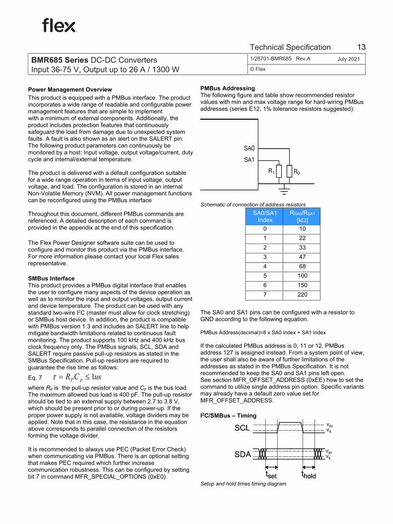
PMBus Addressing The following figure and table show recommended resistor values with min and max voltage range for hard-wiring PMBus addresses (series E12, 1% tolerance resistors suggested):
Schematic of connection of address resistors
SA0/SA1 Index
RSA0/RSA1
[kΩ] 0 10 1 22 2 33 3 47 4 68 5 100 6 150 7 220
The SA0 and SA1 pins can be configured with a resistor to GND according to the following equation. PMBus Address(decimal)=8 x SA0 index + SA1 index If the calculated PMBus address is 0, 11 or 12, PMBus address 127 is assigned instead. From a system point of view, the user shall also be aware of further limitations of the addresses as stated in the PMBus Specification. It is not recommended to keep the SA0 and SA1 pins left open. See section MFR_OFFSET_ADDRESS (0xEE) how to set the command to utilize single address pin option. Specific variants may already have a default zero value set for MFR_OFFSET_ADDRESS. I2C/SMBus – Timing
Setup and hold times timing diagram
BMR685 Series DC-DC Converters Input 36-75 V, Output up to 26 A / 1300 W
1/28701-BMR685 Rev.A July 2021
© Flex
Technical Specification 13

INTERNAL USE ONLY
PRODUCT SPECIFICATION
3 (8) Prepared (Subject resp) No.
JIDIBIBX Li Bo 3/1301-BMR 685 0000Uen Approved (Document resp) Checked Date Rev
JIDIBIBX Li Bo 12/14/20201 B The setup time, tset, is the time data, SDA, must be stable before the rising edge of the clock signal, SCL. The hold time thold, is the time data, SDA, must be stable after the rising edge of the clock signal, SCL. If these times are violated incorrect data may be captured or meta-stability may occur and the bus communication may fail. All standard SMBus protocols must be followed, including clock stretching. This product supports the BUSY flag in the status commands to indicate product being too busy for SMBus response. A bus-free time delay between every SMBus transmission (between every stop & start condition) must occur. Refer to the SMBus specification, for SMBus electrical and timing requirements. Note that an additional delay of 5 ms has to be inserted in case of storing the RAM content into the internal non-volatile memory. Monitoring via PMBus It is possible to continuously monitor a wide variety of parameters through the PMBus interface. These include, but are not limited to, the parameters listed in the table below. Parameter PMBus Command
Input voltage READ_VIN Output voltage READ_VOUT Output current READ_IOUT Temperature * READ_TEMPERATURE_1 Switching Frequency READ_FREQUENCY Duty cycle READ_DUTY_CYCLE *Reports the temperature from temperature sensor set in command 0xDC, internal (controller IC)/external (temp sensor). Monitoring Faults Fault conditions can be detected using the SALERT pin, which will be asserted low when any number of pre-configured fault or warning conditions occurs. The SALERT pin will be held low until faults and/or warnings are cleared by the CLEAR_FAULTS command, or until the output voltage has been re-enabled. It is possible to mask which fault conditions should not assert the SALERT pin by the command SMBALERT_MASK. In response to the SALERT signal, the user may read a number of status commands to find out what fault or warning condition occurred, see table below.
Fault & Warning Status PMBus Command
Overview, Power Good
STATUS_BYTE STAUS_WORD
Output voltage level STATUS_VOUT Output current level STATUS _IOUT Input voltage level STATUS_INPUT Temperature level STATUS_TEMPERATURE PMBus communication STATUS_CML
Snapshot Parameter Capture When input voltage disappears during conversion the Snapshot functionality will automatically store parametric RAM data to NVM. After the module with Vin in the operating range again, it is able to retrieve snap shot data from the previous power. The NVM data can be read back using the MFR_GET_SNAPSHOT (0xD7) command to provide valuable information for analysis. Using the MFR_SNAPSHOT_CYCLES_SELECT (0xD5) command can trace back to the latest snapshot cycles selection with byte. The snap shot parameters called old are the recorded values at the fault event. All other snap shot parameters are stored to NVM when VI falls below VIoff level. Theoretically the snapshot could be corrupted by a very fast Vin drop. Following parameters are stored to NVM:
• Input voltage old • Output voltage old • Output current old • Duty cycle old • Input voltage • Output voltage • Output current • Temperature_1 (sensor select in 0xDC) • Temperature_2 • Time in operation • Status_word • Status_byte • Status_Vout • Status_Iout • Status_Input • Status_Temperature • Status_CML • Snap shot cycles
Read MFR_GET_SNAPSHOT using the Flex Power Designer.
BMR685 Series DC-DC Converters Input 36-75 V, Output up to 26 A / 1300 W
1/28701-BMR685 Rev.A July 2021
© Flex
Technical Specification 14

INTERNAL USE ONLY
PRODUCT SPECIFICATION
4 (8) Prepared (Subject resp) No.
JIDIBIBX Li Bo 3/1301-BMR 685 0000Uen Approved (Document resp) Checked Date Rev
JIDIBIBX Li Bo 12/14/20201 B Non-Volatile Memory (NVM) The product incorporates two Non-Volatile Memory areas for storage of the PMBus command values; the Default NVM and the User NVM. The Default NVM is pre-loaded with Flex factory default values. The Default NVM is write-protected and can be used to restore the Flex factory default values through the command RESTORE_DEFAULT_ALL (0x12). The User NVM is pre-loaded with Flex factory default values. The User NVM is writable and open for customization. The values in NVM are loaded during initialization according to section Initialization Procedure, where after commands can be changed through the PMBus Interface. The STORE_USER_ALL (0x15) command will store the changed parameters to the User NVM. Operating Information Input Voltage The input voltage range 36 to 75 Vdc meets the requirements for normal input voltage range in –48 Vdc systems. The absolute maximum continuous input voltage is 75 Vdc. Short duration transient disturbances can occur on the DC distribution and input of the product when a short circuit fault occurs on the equipment side of a protective device (fuse or circuit breaker). The voltage level, duration and energy of the disturbance are dependent on the particular DC distribution network characteristics and can be sufficient to damage the product unless measures are taken to suppress or absorb this energy. The transient voltage can be limited by capacitors and other energy absorbing devices like zener diodes connected across the positive and negative input conductors at a number of strategic points in the distribution network. The end-user must secure that the transient voltage will not exceed the value stated in the Absolute maximum ratings. ETSI TR 100 283 examines the parameters of DC distribution networks and provides guidelines for controlling the transient and reduce its harmful effect. Turn-on and -off Input Voltage The product monitors the input voltage and will turn on and turn off at configured thresholds (see Electrical Specification). The turn-on input voltage voltage threshold is set higher than the corresponding turn-off threshold. Hence, there is a hysteresis between turn-on and turn-off input voltage levels. Remote Control (RC)
The products are fitted with a remote control function referenced to the primary negative input connection (-In), with negative and positive logic options available. The RC function allows the product to be turned on/off by an external device like a semiconductor or mechanical switch.
The RC pin has an internal pull up resistor. The external device must provide a minimum required sink current >1.5 mA to guarantee a voltage not higher than maximum voltage on the RC pin (see Electrical characteristics table). To turn off the product the RC pin should be left open for a minimum of time 150 µs, the same time requirement applies when the product shall turn on. When the RC pin is left open, the voltage generated on the RC pin is max 5 V. The standard product is provided with “negative logic” RC and will be off until the RC pin is connected to the –In. To turn off the product the RC pin should be left open. In situations where it is desired to have the product to power up automatically without the need for control signals or a switch, the RC pin shall be wired directly to –In. Input and Output Impedance The impedance of both the input source and the load will interact with the impedance of the product. It is important that the input source has low characteristic impedance. Minimum recommended external input capacitance is 470 µF. The electrolytic capacitors will be degraded in low temperature. The needed input capacitance in low temperature should be equivalent to 470 µF at 20°C. The performance in some applications can be enhanced by addition of external capacitance as described under External Decoupling Capacitors. If the input voltage source contains significant inductance, the addition of a low ESR ceramic capacitor of 22 – 100 µF capacitor across the input of the product will ensure stable operation. The minimum required capacitance value depends on the output power and the input voltage. The higher output power the higher input capacitance is needed.
BMR685 Series DC-DC Converters Input 36-75 V, Output up to 26 A / 1300 W
1/28701-BMR685 Rev.A July 2021
© Flex
Technical Specification 15

INTERNAL USE ONLY
PRODUCT SPECIFICATION
5 (8) Prepared (Subject resp) No.
JIDIBIBX Li Bo 3/1301-BMR 685 0000Uen Approved (Document resp) Checked Date Rev
JIDIBIBX Li Bo 12/14/20201 B External Decoupling Capacitors When powering loads with significant dynamic current requirements, the voltage regulation at the point of load can be improved by addition of decoupling capacitors at the load. The most effective technique is to locate low ESR ceramic and electrolytic capacitors as close to the load as possible, using several parallel capacitors to lower the effective ESR. The ceramic capacitors will handle high-frequency dynamic load changes while the electrolytic capacitors are used to handle low frequency dynamic load changes. It is equally important to use low resistance and low inductance PWB layouts and cabling. External decoupling capacitors will become part of the product’s control loop. The control loop is optimized for a wide range of external capacitance and the maximum recommended value that could be used without any additional analysis is found in the Electrical specification. The ESR of the capacitors is a very important parameter. Stable operation is guaranteed with a verified ESR value of >1 mΩ across the output connections. For further information please contact your local Flex Power Modules representative. PMBus configuration and support The product provides a PMBus digital interface that enables the user to configure many aspects of the device operation as well as monitor the input and output parameters. The Flex Power Designer software suite can be used to configure and monitor this product via the PMBus interface. For more information, please contact your local Flex sales representative. Output Voltage Adjust using PMBus The output voltage of the product can be reconfigured via PMBus command VOUT_COMMAND (0x21) or VOUT_TRIM (0x22). This can be used when adjusting the output voltage above or below output voltage initial setting up to a certain level, see Electrical specification for adjustment range. When increasing the output voltage, the voltage at the output pins must be kept within the plotted area, see graph. Output voltage setting must be kept below the threshold of the over voltage protection, (OVP) to prevent the product from shutting down. At increased output voltages the maximum power rating of the product remains the same, and the max output current must be decreased correspondingly.
Margin Up/Down Controls These controls allow the output voltage to be momentarily adjusted, either up or down, by a nominal 10%. The margin high and margin low shall be limited to max and min output voltage, if the nominal output voltage is changed. This provides a convenient method for dynamically testing the operation of the load circuit over its supply margin or range. It can also be used to verify the function of supply voltage supervisors. The margin up and down levels of the product can easily be re-configured using Flex Power Designer software. Soft-start Power Up
The default rise time for a single product is 100 ms. When starting by applying input voltage the control circuit boot-up time adds an additional 60 ms delay. The soft-start and soft-stop control functionality allows the output voltage to ramp-up and ramp-down with defined timing with respect to the control of the output. This can be used to control inrush current and manage supply sequencing of multiple controllers. The rise time is the time taken for the output to ramp to its target voltage, while the fall time is the time taken for the output to ramp down from its regulation voltage to 0 V. The TON_DELAY (0x60) time sets a delay from when the output is enabled until the output voltage starts to ramp up. The TOFF_DELAY (0x64) delay time sets a delay from when the output is disabled until the output voltage starts to ramp down. Output control
VOUT
On Delay Time
On Ramp time
Off Ramp Time
Off Delay Time
Illustration of Soft-Start and Soft-Stop. By default, soft-stop is disabled, and the regulation of output voltage stops immediately when the output is disabled. Soft-stop can be enabled through the PMBus command ON_OFF_CONFIG (0x02). The delay and ramp times can be reconfigured using the PMBus commands TON_DELAY (0x60), TON_RISE (0x61), TOFF_DELAY (0x64) and TOFF_FALL (0x65). Pre-bias Start-up The product has a Pre-bias start up functionality and will not sink current during start up if a pre-bias source is present at the output terminals. If the Pre-bias voltage is lower than the target value set in VOUT_COMMAND (0x21), the product will ramp up to the target value. If the Pre-bias voltage is higher than the target value set in VOUT_COMMAND (0x21), the product will ramp down to the target value and in this case sink current for a time interval set by the command TOFF_MAX_WARN_LIMIT (0x66).
OTP, UTP (Over/Under Temperature Protection) The products are protected from thermal overload by an internal over temperature sensor. The product will make continuous attempts to start up (non-latching mode) and resume normal operation automatically when the temperature has dropped below the temperature threshold set in command OT_WARN_LIMIT (0x51). The OTP and hysteresis of the product can be re-configured using the PMBus interface. The product has also an under-temperature protection. The OTP and UTP fault limit and fault response can be configured via the PMBus. Note: using the
BMR685 Series DC-DC Converters Input 36-75 V, Output up to 26 A / 1300 W
1/28701-BMR685 Rev.A July 2021
© Flex
Technical Specification 16

INTERNAL USE ONLY
PRODUCT SPECIFICATION
6 (8) Prepared (Subject resp) No.
JIDIBIBX Li Bo 3/1301-BMR 685 0000Uen Approved (Document resp) Checked Date Rev
JIDIBIBX Li Bo 12/14/20201 B fault response “Ignore Fault” may cause permanent damage to the product Input Under Voltage Protection The product can be protected from high input voltage and low input voltage. The under-voltage fault level and fault response is easily configured using Flex Power Designer software, see also Appendix – PMBus commands. OVP (Output Over Voltage Protection) The product includes over voltage limiting circuitry for protection of the load. The default OVP limit is 20% above the nominal output voltage. If the output voltage exceeds the OVP limit, the product can respond in different ways. The default response from an over voltage fault is to immediately shut down. The device will continuously check for the presence of the fault condition, and when the fault condition no longer exists the device will be re-enabled. The OVP fault level and fault response can be configured via the PMBus interface, see Appendix – PMBus commands. OCP (Over Current Protection) The products include current limiting circuitry for protection at continuous overload. then shutdown and automatic restart for output currents in excess of max output current (max IO). The product will resume normal operation after removal of the overload. The load distribution should be designed for the maximum output short circuit current specified. The over current protection of the product can be configured via the PMBus interface, see Appendix – PMBus commands. Switching frequency The switching frequency is set to 120 kHz as default but this can not be reconfigured via the PMBus interface. Power Good The power good pin 7 (PG) indicates when the product is ready to provide regulated output voltage to the load. During ramp-up and during a fault condition, PG is held high. By default, PG is asserted low after the output has ramped to a voltage above 40 V, and de-asserted if the output voltage falls below 30 V. These thresholds may be changed using the PMBus commands POWER_GOOD_ON (0x5E) and POWER_GOOD_OFF (0x5F). The polarity is by default configured to active low, the polarity of PG can be set to active high in the command MFR_PGOOD_POLARITY (0xD0): 0xD0 = 00 (active low) 0xD0 = 01 (active high) The product provides Power Good flag in the Status Word register that indicates the output voltage is within a specified tolerance of its target level and no-fault condition exists.
Address Offset The command MFR_OFFSET_ADDRESS (0xEE) is used to configure an address offset. The PMBus-address offset’s value increments the address value following the formula in the PMBus Addressing section of documentation. See Appendix – PMBus commands. Output Voltage Adjust (Trim) The products have an Output Voltage Adjust pin (Trim),pin7. This pin can be used to adjust the output voltage above or below Output voltage initial setting. It is possible to change output voltage either by using passive components or active (dependent current source). If using a resistor to increase the voltage the resistor should be connected between the Trim pin and +Sense pin. The resistor value of the Output voltage adjust function is according to information given under the Output section for the respective product. To decrease the output voltage, the resistor should be connected between the Trim pin and –Sense pin. For active control and trim resistor values, please refer to the Typical characteristics section.
Remote Sense The products have remote sense that can be used to compensate for voltage drops between the output and the point of load. The sense traces should be located close to the PWB ground layer to reduce noise susceptibility. The remote sense circuitry will compensate for up to 10% voltage drop between output pins and the point of load. If the remote sense is not needed +Sense should be connected to +Out and -Sense should be connected to -Out.
BMR685 Series DC-DC Converters Input 36-75 V, Output up to 26 A / 1300 W
1/28701-BMR685 Rev.A July 2021
© Flex
Technical Specification 17

INTERNAL USE ONLY
PRODUCT SPECIFICATION
7 (8) Prepared (Subject resp) No.
JIDIBIBX Li Bo 3/1301-BMR 685 0000Uen Approved (Document resp) Checked Date Rev
JIDIBIBX Li Bo 12/14/20201 B Thermal Consideration General The products are designed to operate in different thermal environments and sufficient cooling must be provided to ensure reliable operation. For products mounted on a PWB without a heat sink attached, cooling is achieved mainly by conduction, from the pins to the host board, and convection, which is dependent on the airflow across the product. Increased airflow enhances the cooling of the product. The Output Current Derating graph found in the Output section for each model provides the available output current vs. ambient air temperature and air velocity at VI = 48 V. The product is tested on a 254 x 254 mm, 35 µm (1 oz), 16-layer test board mounted vertically in a wind tunnel with a cross-section of 608 x 203 mm.
For products with base plate used in a sealed box/cold wall application, cooling is achieved mainly by conduction through the cold wall. The Output Current Derating graphs are found in the Output section for each model. The product is tested in a sealed box test set up with ambient temperatures 85°C. See Design Note 028 for further details.
Definition of product operating temperature The product operating temperatures is used to monitor the temperature of the product, and proper thermal conditions can be verified by measuring the temperature at positions P1 and P2. The temperature at these positions (TP1, TP2) should not exceed the maximum temperatures in the table below. The number of measurement points may vary with different thermal design and topology. Temperatures above maximum TP1, measured at the reference point P1 are not allowed and may cause permanent damage. Position Description Max Temp. P1 PCB TP1=125º C
P2 Base plate TP2=100º C
Reference point on pin side
10111213141516
P1
BMR685 Series DC-DC Converters Input 36-75 V, Output up to 26 A / 1300 W
1/28701-BMR685 Rev.A July 2021
© Flex
Technical Specification 18

INTERNAL USE ONLY
PRODUCT SPECIFICATION
8 (8) Prepared (Subject resp) No.
JIDIBIBX Li Bo 3/1301-BMR 685 0000Uen Approved (Document resp) Checked Date Rev
JIDIBIBX Li Bo 12/14/20201 B
Reference point on top side
Connections (Reference point on pin side)
Pin Designation Function 1 +In Positive Input 2 RC Remote Control 3 NC NC 4 -In Negative Input 5 -Out Negative Output 6 -sense Negative Remote Sense 7 Trim Output Voltage adjust 8 +sense Positive Remote Sense
9 +Out Positive Output
10 Ctrl/ PG PMBus Remote control/ Power Good
11 DGND PMBus ground 12 SDA PMBus Data 13 SALERT PMBus alert signal 14 SCL PMBus Clock 15 SA1 PMBus Address 1 16 SA0 PMBus Address 0
10111213141516
P2
BMR685 Series DC-DC Converters Input 36-75 V, Output up to 26 A / 1300 W
1/28701-BMR685 Rev.A July 2021
© Flex
Technical Specification 19
INTERNAL USE ONLY PRODUCT SPEC. MECHANICAL
1 (2)
Prepared (Subject resp) No.
jiddliaa Donnie Li(JID) 4/1301-BMR 685 Uen Approved (Document resp) Checked Date Rev
Jessie Li Li Sun 3/26/2021 B
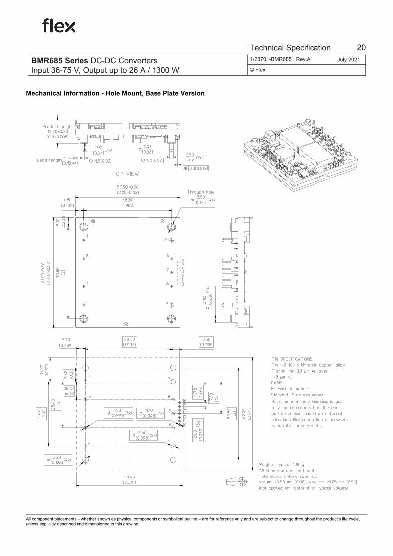
Mechanical Information - Hole Mount, Base Plate Version
All component placements – whether shown as physical components or symbolical outline – are for reference only and are subject to change throughout the product’s life cycle, unless explicitly described and dimensioned in this drawing.
BMR685 Series DC-DC Converters Input 36-75 V, Output up to 26 A / 1300 W
1/28701-BMR685 Rev.A July 2021
© Flex
Technical Specification 20

INTERNAL USE ONLY PRODUCT SPEC. 1 (2)
Prepared (Subject resp) No.
jiddliaa Donnie Li(JID) 5/1301-BMR 685 Approved (Document resp) Checked Date Rev
jidjliaa See §1 12/16/2020 A
Soldering Information - Hole Mounting The hole mounted product is intended for plated through hole mounting by wave or manual soldering. The pin temperature is specified to maximum to 270°C for maximum 10 seconds.
A maximum preheat rate of 4°C/s and maximum preheat temperature of 150°C is suggested. When soldering by hand, care should be taken to avoid direct contact between the hot soldering iron tip and the pins for more than a few seconds in order to prevent overheating.
A no-clean flux is recommended to avoid entrapment of cleaning fluids in cavities inside the product or between the product and the host board. The cleaning residues may affect long time reliability and isolation voltage.
Delivery Package Information The products are delivered in antistatic trays.
Tray Specifications Material Antistatic PE Foam Surface resistance 105 < Ohm/square < 1011 Bakability The trays are not bakable Box capacity 30 products (3 full tray/box)
Tray weight Product – Baseplate Version 140 g empty, 1220 g full tray
BMR685 Series DC-DC Converters Input 36-75 V, Output up to 26 A / 1300 W
1/28701-BMR685 Rev.A July 2021
© Flex
Technical Specification 21

INTERNAL USE ONLY PRODUCT SPEC. 2 (2)
Prepared (Subject resp) No.
jiddliaa Donnie Li(JID) 5/1301-BMR 685 Approved (Document resp) Checked Date Rev
jidjliaa See §1 12/16/2020 A
Product Qualification Specification Characteristics External visual inspection IPC-A-610
Change of temperature (Temperature cycling) IEC 60068-2-14 Na
Temperature range Number of cycles Dwell/transfer time
-40 to 100°C100015 min/0-1 min
Cold (in operation) IEC 60068-2-1 Ad Temperature TA Duration
-45°C72 h
Damp heat IEC 60068-2-67 Cy Temperature Humidity Duration
85°C 85 % RH 1000 hours
Dry heat IEC 60068-2-2 Bd Temperature Duration
125°C 1000 h
Electrostatic discharge susceptibility
IEC 61340-3-1, JESD 22-A114 IEC 61340-3-2, JESD 22-A115
Human body model (HBM) Machine Model (MM)
Class 2, 2000 V Class 3, 200 V
Immersion in cleaning solvents IEC 60068-2-45 XA, method 2 Water Glycol ether
55°C 35°C
Mechanical shock IEC 60068-2-27 Ea Peak acceleration Duration
100 g 6 ms
Operational life test MIL-STD-202G, method 108A Duration 1000 h
Resistance to soldering heat 2 IEC 60068-2-20 Tb, method 1A Solder temperature Duration
270°C 10-13 s
Robustness of terminations IEC 60068-2-21 Test Ua1 IEC 60068-2-21 Test Ue1
Through hole mount products Surface mount products
All leads All leads
Solderability
IEC 60068-2-58 test Td Preconditioning Temperature, SnPb Eutectic Temperature, Pb-free
150°C dry bake 16 h 215°C 235°C
Vibration, broad band random IEC 60068-2-64 Fh, method 1 Frequency Spectral density Duration
10 to 500 Hz 0.07 g2/Hz 10 min in each direction
BMR685 Series DC-DC Converters Input 36-75 V, Output up to 26 A / 1300 W
1/28701-BMR685 Rev.A July 2021
© Flex
Technical Specification 22

PUBLIC
PRODUCT SPECIFICATION
2 (39) Prepared (Subject resp) No.
jidwwang Wenfa Wang 6/1301-BMR685XXXX/820 Approved (Document resp) Checked Date Rev
jidwwang Wenfa Wang 9/5/2020 A PMBus Command Appendix
This appendix contains a detailed reference of the PMBus commands supported by the product. Data Formats The products make use of a few standardized numerical formats, along with custom data formats. A detailed walkthrough of the above formats is provided in AN304, as well as in sections 7 and 8 of the PMBus Specification Part II. The custom data formats vary depending on the command, and are detailed in the command description. Standard Commands The functionality of commands with code 0x00 to 0xCF is usually based on the corresponding command specification provided in the PMBus Standard Specification Part II (see Power System Management Bus Protocol Documents below). However there might be different interpretations of the PMBus Standard Specification or only parts of the Standard Specification applied, thus the detailed command description below should always be consulted. Forum Websites The System Management Interface Forum (SMIF) http://www.powersig.org/ The System Management Interface Forum (SMIF) supports the rapid advancement of an efficient and compatible technology base that promotes power management and systems technology implementations. The SMIF provides a membership path for any company or individual to be active participants in any or all of the various working groups established by the implementer forums. Power Management Bus Implementers Forum (PMBUS-IF) http://pmbus.org/ The PMBus-IF supports the advancement and early adoption of the PMBus protocol for power management. This website offers recent PMBus specification documents, PMBus articles, as well as upcoming PMBus presentations and seminars, PMBus Document Review Board (DRB) meeting notes, and other PMBus related news. PMBus – Power System Management Bus Protocol Documents These specification documents may be obtained from the PMBus-IF website described above. These are required reading for complete understanding of the PMBus implementation. This appendix will not re-address all of the details contained within the two PMBus Specification documents. Specification Part I – General Requirements Transport And Electrical Interface Includes the general requirements, defines the transport and electrical interface and timing requirements of hard wired signals. Specification Part II – Command Language Describes the operation of commands, data formats, fault management and defines the command language used with the PMBus. SMBus – System Management Bus Documents System Management Bus Specification, Version 2.0, August 3, 2000 This specification specifies the version of the SMBus on which Revision 1.2 of the PMBus Specification is based. This specification is freely available from the System Management Interface Forum Web site at: http://www.smbus.org/specs/
BMR685 Series DC-DC Converters Input 36-75 V, Output up to 26 A / 1300 W
1/28701-BMR685 Rev.A July 2021
© Flex
Technical Specification 23

PUBLIC
PRODUCT SPECIFICATION
3 (39) Prepared (Subject resp) No.
jidwwang Wenfa Wang 6/1301-BMR685XXXX/820 Approved (Document resp) Checked Date Rev
jidwwang Wenfa Wang 9/5/2020 A
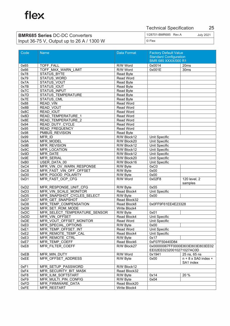
Code Name Data Format Factory Default Value
Standard Configuration BMR 685 XXXX/000 R1
0x01 OPERATION R/W Byte 0x84 0x02 ON_OFF_CONFIG R/W Byte 0x1B 0x03 CLEAR_FAULTS Send Byte 0x10 WRITE_PROTECT R/W Byte 0x11 STORE_DEFAULT_ALL Send Byte 0x12 RESTORE_DEFAULT_ALL Send Byte 0x15 STORE_USER_ALL Send Byte 0x16 RESTORE_USER_ALL Send Byte 0x19 CAPABILITY Read Byte 0x20 VOUT_MODE Read Byte 0x16 0x21 VOUT_COMMAND R/W Word 0xC800 50.0 V 0x22 VOUT_TRIM R/W Word 0x0000 0.0 V 0x23 VOUT_CAL_OFFSET R/W Word Unit Specific 0x24 VOUT_MAX R/W Word 0xE400 57.0 V 0x25 VOUT_MARGIN_HIGH R/W Word 0xC800 50.0 V 0x26 VOUT_MARGIN_LOW R/W Word 0xB400 45.0 V 0x27 VOUT_TRANSITION_RATE R/W Word 0x9B02 0.1 V/ms 0x28 VOUT_DROOP R/W Word 0xE800 0.0 mV/A 0x29 VOUT_SCALE_LOOP R/W Word Unit Specific 0x2A VOUT_SCALE_MONITOR R/W Word Unit Specific 0x32 MAX_DUTY R/W Word 0xEB00 96.0 % 0x33 FREQUENCY_SWITCH R/W Word 0x0078 120.0 kHz 0x35 VIN_ON R/W Word 0xE220 34.0 V 0x36 VIN_OFF R/W Word 0xE200 32.0 V 0x39 IOUT_CAL_OFFSET Read Word Unit Specific 0x40 VOUT_OV_FAULT_LIMIT R/W Word 0xEC00 59.0 V 0x41 VOUT_OV_FAULT_RESPONSE R/W Byte 0xC0 0x42 VOUT_OV_WARN_LIMIT R/W Word 0xEC00 59.0 V 0x43 VOUT_UV_WARN_LIMIT R/W Word 0x0000 0.0 V 0x44 VOUT_UV_FAULT_LIMIT R/W Word 0x0000 0.0 V 0x45 VOUT_UV_FAULT_RESPONSE R/W Byte 0x00 0x46 IOUT_OC_FAULT_LIMIT R/W Word 0xE200 32.0 A 0x47 IOUT_OC_FAULT_RESPONSE R/W Byte 0xC3 0x48 IOUT_OC_LV_FAULT_LIMIT R/W Word 0x8533 33.3 V 0x4A IOUT_OC_WARN_LIMIT R/W Word 0xDBA0 29.0 A 0x4F OT_FAULT_LIMIT R/W Word 0xEBEB 125.0 °C 0x50 OT_FAULT_RESPONSE R/W Byte 0xC0 0x51 OT_WARN_LIMIT R/W Word 0xEB20 100.0 °C 0x52 UT_WARN_LIMIT R/W Word 0xE580 -40.0 °C 0x53 UT_FAULT_LIMIT R/W Word 0xE4E0 -50.0 °C 0x54 UT_FAULT_RESPONSE R/W Byte 0xC0 0x55 VIN_OV_FAULT_LIMIT R/W Word 0x004E 78.0 V 0x56 VIN_OV_FAULT_RESPONSE R/W Byte 0xC0 0x57 VIN_OV_WARN_LIMIT R/W Word 0x004E 78.0 V 0x58 VIN_UV_WARN_LIMIT R/W Word 0x0000 0.0 V 0x59 VIN_UV_FAULT_LIMIT R/W Word 0x0000 0.0 V 0x5A VIN_UV_FAULT_RESPONSE R/W Byte 0x00 0x5E POWER_GOOD_ON R/W Word 0xA000 40.0 V 0x5F POWER_GOOD_OFF R/W Word 0x7800 30.0 V 0x60 TON_DELAY R/W Word 0x00FA 250ms 0x61 TON_RISE R/W Word 0x0064 100ms 0x62 TON_MAX_FAULT_LIMIT R/W Word 0x000F 15ms 0x63 TON_MAX_FAULT_RESPONSE R/W Byte 0x00 0x64 TOFF_DELAY R/W Word 0x0005
PMBus Command Summary and Factory Default Values of Standard Configuration The factory default values provided in the table below are valid for the Standard configuration. Factory default values for other configurations can be found using the Flex Power Designer tool.
BMR685 Series DC-DC Converters Input 36-75 V, Output up to 26 A / 1300 W
1/28701-BMR685 Rev.A July 2021
© Flex
Technical Specification 24
PUBLIC
PRODUCT SPECIFICATION
4 (39) Prepared (Subject resp) No.
jidwwang Wenfa Wang 6/1301-BMR685XXXX/820 Approved (Document resp) Checked Date Rev
jidwwang Wenfa Wang 9/5/2020 A
Code Name Data Format Factory Default Value Standard Configuration BMR 685 XXXX/000 R1
0x65 TOFF_FALL R/W Word 0x0014 20ms 0x66 TOFF_MAX_WARN_LIMIT R/W Word 0x001E 30ms 0x78 STATUS_BYTE Read Byte 0x79 STATUS_WORD Read Word 0x7A STATUS_VOUT Read Byte 0x7B STATUS_IOUT Read Byte 0x7C STATUS_INPUT Read Byte 0x7D STATUS_TEMPERATURE Read Byte 0x7E STATUS_CML Read Byte 0x88 READ_VIN Read Word 0x8B READ_VOUT Read Word 0x8C READ_IOUT Read Word 0x8D READ_TEMPERATURE_1 Read Word 0x8E READ_TEMPERATURE_2 Read Word 0x94 READ_DUTY_CYCLE Read Word 0x95 READ_FREQUENCY Read Word 0x98 PMBUS_REVISION Read Byte 0x99 MFR_ID R/W Block12 Unit Specific 0x9A MFR_MODEL R/W Block20 Unit Specific 0x9B MFR_REVISION R/W Block12 Unit Specific 0x9C MFR_LOCATION R/W Block12 Unit Specific 0x9D MFR_DATE R/W Block12 Unit Specific 0x9E MFR_SERIAL R/W Block20 Unit Specific 0xB0 USER_DATA_00 R/W Block16 Unit Specific 0xC4 MFR_VIN_OV_WARN_RESPONSE R/W Byte 0xC0 0xC8 MFR_FAST_VIN_OFF_OFFSET R/W Byte 0x00 0xD0 MFR_PGOOD_POLARITY R/W Byte 0x00 0xD1 MFR_FAST_OCP_CFG R/W Word 0x02F8 120 level, 2
samples 0xD2 MFR_RESPONSE_UNIT_CFG R/W Byte 0x55 0xD3 MFR_VIN_SCALE_MONITOR Read Block4 Unit Specific 0xD5 MFR_SNAPSHOT_CYCLES_SELECT R/W Byte 0x00 0xD7 MFR_GET_SNAPSHOT Read Block32 0xD8 MFR_TEMP_COMPENSATION Read Block8 0x0FF9F61EE4E23328 0xD9 MFR_SET_ROM_MODE Write Block4 0xDC MFR_SELECT_TEMPERATURE_SENSOR R/W Byte 0x01 0xDD MFR_VIN_OFFSET Read Block4 Unit Specific 0xDE MFR_VOUT_OFFSET_MONITOR Read Word Unit Specific 0xE0 MFR_SPECIAL_OPTIONS R/W Byte 0x00 0xE1 MFR_TEMP_OFFSET_INT Read Word Unit Specific 0xE2 MFR_REMOTE_TEMP_CAL Read Block4 Unit Specific 0xE3 MFR_REMOTE_CTRL R/W Byte 0x17 0xE7 MFR_TEMP_COEFF Read Block6 0xF07F50440D84 0xE8 MFR_FILTER_COEFF R/W Block27 0x00000067FF0000E803E803E803EE02
EE02EE02320010271027AC0D 0xEB MFR_MIN_DUTY R/W Word 0x1941 25 ns, 65 ns 0xEE MFR_OFFSET_ADDRESS R/W Byte 0x00 n + 8 x SA0 index +
SA1 index 0xF1 MFR_SETUP_PASSWORD R/W Block12 0xF4 MFR_SECURITY_BIT_MASK Read Block32 0xF8 MFR_ILIM_SOFTSTART R/W Byte 0x14 20 % 0xF9 MFR_MULTI_PIN_CONFIG R/W Byte 0x04 0xFD MFR_FIRMWARE_DATA Read Block20 0xFE MFR_RESTART Write Block4
BMR685 Series DC-DC Converters Input 36-75 V, Output up to 26 A / 1300 W
1/28701-BMR685 Rev.A July 2021
© Flex
Technical Specification 25
PUBLIC
PRODUCT SPECIFICATION
5 (39) Prepared (Subject resp) No.
jidwwang Wenfa Wang 6/1301-BMR685XXXX/820 Approved (Document resp) Checked Date Rev
jidwwang Wenfa Wang 9/5/2020 A
Bit Function Description Value Function Description 7:6 Enable Make the device enable or
disable. 00 Immediate Off Disable Immediately without
sequencing. 01 Soft Off Disable "Softly" with
sequencing. 10 Enable Enable device to the desired
margin state. 5:4 Margin Select between margin high/low
states or nominal output. 00 Nominal Operate at nominal output
voltage. 01 Margin Low Operate at margin low voltage
set in VOUT_MARGIN_LOW. 10 Margin High Operate at margin high voltage
set in VOUT_MARGIN_HIGH. 3:2 Act on Fault Set 10b to act on fault or set to
01b to ignore fault. 01 Ignore Faults Ignore Faults when in a
margined state. The device will ignore appropriate overvoltage/undervoltage warnings and faults and respond as programmed by the warning limit or fault response command.
10 Act on Faults Act on Faults when in a margined state. The device will handle appropriate overvoltage/undervoltage warnings and faults and respond as programmed by the warning limit or fault response command.
Bit Function Description Value Function Description 4 Powerup
Operation Sets the default to either operate any time power is present or for the on/off to be controlled by CONTROL pin and serial bus commands.
0 Enable Always Unit powers up any time power is present regardless of state of the CONTROL pin.
1 Enable pin or PMBus
Unit does not power up until commanded by the CONTROL pin and OPERATION command.
3 PMBus Enable Mode
Controls how the unit responds to commands received via the serial bus.
0 Ignore PMBus Unit ignores the on/off portion of the OPERATION command from serial bus.
1 Use PMBus To start, the unit requires that the on/off portion of the OPERATION command is instructing the unit to run.
2 Enable Pin Mode
Controls how the unit responds to the CONTROL pin.
0 Ignore pin Unit ignores the CONTROL/Enable pin.
1 Use pin Unit requires the CONTROL pin to be asserted to start the unit.
1 Enable Pin Polarity
Polarity of the CONTROL pin. 0 Active Low Enable pin will cause device to enable when driven low.
1 Active High Enable pin will cause device to enable when driven high.
0 Disable Action CONTROL pin action when commanding the unit to turn off.
0 Soft Off Use the programmed turn off delay and fall time.
PMBus Command Details
OPERATION (0x01) Description: Sets the desired PMBus enable and margin operations.
ON_OFF_CONFIG (0x02) Description: Configures how the device is controlled by the CONTROL pin and the PMBus.
BMR685 Series DC-DC Converters Input 36-75 V, Output up to 26 A / 1300 W
1/28701-BMR685 Rev.A July 2021
© Flex
Technical Specification 26

PUBLIC
PRODUCT SPECIFICATION
6 (39) Prepared (Subject resp) No.
jidwwang Wenfa Wang 6/1301-BMR685XXXX/820 Approved (Document resp) Checked Date Rev
jidwwang Wenfa Wang 9/5/2020 A
Bit Function Description Value Function Description 1 Imm. Off Turn off the output and stop
transferring energy to the output as fast as possible. The device's product literature shall specify whether or not the device sinks current to decrease the output voltage fall time.
Bit Description Value Function Description 7:0 All supported commands may have their parameters
read, regardless of the WRITE_PROTECT settings. 0x80 Disable all
writes Disable all writes except to the WRITE_PROTECT command.
0x40 Enable operation
Disable all writes except to the WRITE_PROTECT, OPERATION and PAGE commands.
0x20 Enable control and Vout commands
Disable all writes except to the WRITE_PROTECT, OPERATION, PAGE, ON_OFF_CONFIG and VOUT_COMMAND commands.
0x00 Enable all commands
Enable writes to all commands.
Bit Function Description Value Function Description 7 Packet Error
Checking Packet error checking. 00 Not supported Packet Error Checking not
supported. 01 Supported Packet Error Checking is
supported. 6:5 Maximum Bus
Speed Maximum bus speed. 00 100kHz Maximum supported bus speed
is 100 kHz. 01 400kHz Maximum supported bus speed
is 400 kHz. 3:0 Smbalert SMBALERT 00 No Smbalert The device does not have a
SMBALERT# pin and does not support the SMBus Alert Response protocol.
CLEAR_FAULTS (0x03) Description: Clears all fault status bits
WRITE_PROTECT (0x10) Description: The WRITE_PROTECT command is used to control writing to the PMBus device. The intent of this command is to provide protection against accidental changes. This command is not intended to provide protection against deliberate or malicious changes to a device’s configuration or operation.
STORE_DEFAULT_ALL (0x11) Description: Commands the device to store its configuration into the Default Store.
RESTORE_DEFAULT_ALL (0x12) Description: Commands the device to restore its configuration from the Default Store.
STORE_USER_ALL (0x15) Description: Stores, at the USER level, all PMBus values that were changed since the last restore command.
RESTORE_USER_ALL (0x16) Description: Restores PMBus settings that were stored using STORE_USER_ALL. This command is automatically performed at power up.
CAPABILITY (0x19) Description: This command provides a way for a host system to determine some key capabilities of a PMBus device.
BMR685 Series DC-DC Converters Input 36-75 V, Output up to 26 A / 1300 W
1/28701-BMR685 Rev.A July 2021
© Flex
Technical Specification 27

PUBLIC
PRODUCT SPECIFICATION
7 (39) Prepared (Subject resp) No.
jidwwang Wenfa Wang 6/1301-BMR685XXXX/820 Approved (Document resp) Checked Date Rev
jidwwang Wenfa Wang 9/5/2020 A
Bit Function Description Value Function Description 01 Have Smbalert The device does have a
SMBALERT# pin and does support the SMBus Alert Response protocol.
Bit Function Description Format 4:0 Five bit two's complement EXPONENT for the MANTISSA delivered as the
data bytes for VOUT_COMMAND in VOUT_LINEAR Mode, five bit VID code identifier per in VID Mode or always set to 00000b in Direct Mode.
Integer Signed
Bit Function Description Value Function Description 7:5 Set to 000b to select
VOUT_LINEAR Mode (Five bit two's complement exponenet for the MANTISSA delivered as the data bytes for an output voltage related command), set to 001b to select VID Mode (Five bit VID code identifier per) or set to 010b to select Direct Mode (Always set to 00000b).
000 Linear Linear Mode Format. 001 VID VID Mode. 010 Direct Direct Mode.
Bit Description Format Unit 15:0 Sets the nominal value of the output voltage. Vout Mode
Unsigned V
Bit Description Format Unit 15:0 Sets VOUT trim value. The two bytes are formatted as a two's complement binary mantissa,
used in conjunction with the exponent set in VOUT_MODE. Vout Mode Signed
V
Bit Description Format Unit 15:0 Vout calibration value. It is a signed number in Vout linear mode. The setting will be applied
output voltage. Vout Mode Signed
V
Bit Description Format Unit 15:0 Sets the maximum possible value setting of VOUT. The maximum VOUT_MAX setting is
110% of the pin-strap setting. Vout Mode Unsigned
V
Bit Description Format Unit 15:0 Sets the value of the VOUT during a margin high. Vout Mode
Unsigned V
VOUT_MODE (0x20) Description: Controls how future VOUT-related commands parameters will be interpreted.
VOUT_COMMAND (0x21) Description: Commands the device to transition to a new output voltage.
VOUT_TRIM (0x22) Description: Configures a fixed offset to be applied to the output voltage when enabled.
VOUT_CAL_OFFSET (0x23) Description: Vout calibration value. It is a signed number in Vout linear mode. The setting will be applied output voltage.
VOUT_MAX (0x24) Description: Configures the maximum allowed output voltage.
VOUT_MARGIN_HIGH (0x25) Description: Configures the target for margin-up commands.
BMR685 Series DC-DC Converters Input 36-75 V, Output up to 26 A / 1300 W
1/28701-BMR685 Rev.A July 2021
© Flex
Technical Specification 28

PUBLIC
PRODUCT SPECIFICATION
8 (39) Prepared (Subject resp) No.
jidwwang Wenfa Wang 6/1301-BMR685XXXX/820 Approved (Document resp) Checked Date Rev
jidwwang Wenfa Wang 9/5/2020 A
Bit Description Format Unit 15:0 Sets the value of the VOUT during a margin low. Vout Mode
Unsigned V
Bit Description Format Unit 15:0 Sets the transition rate during margin or other change of VOUT. Linear V/ms
Bit Description Format Unit 15:0 Sets the effective load line (V/I slope) for the rail in which the device is used. Linear mV/A
Bit Description Format 15:0 Gain of Vout EADC sense. Direct
Bit Description Format 15:0 Normally there is a voltage divider in the voltage sense circuit. The scale factor is
represented by VOUT_SCALE_MONITOR. Direct
Bit Description Format Unit 15:0 Sets the maximum allowable duty cycle of the switching frequency. Linear %
Bit Description Format Unit 15:0 Sets the switching frequency. Linear kHz
Bit Description Format Unit 15:0 Sets the VIN ON threshold. Linear V
Bit Description Format Unit 15:0 Sets the VIN OFF threshold. Linear V
VOUT_MARGIN_LOW (0x26) Description: Configures the target for margin-down commands.
VOUT_TRANSITION_RATE (0x27) Description: Configures the transition time for margins and VCOMMAND output changes.
VOUT_DROOP (0x28) Description: Configures the Isense voltage to load current ratio.
VOUT_SCALE_LOOP (0x29) Description: Gain of Vout EADC sense.
VOUT_SCALE_MONITOR (0x2A) Description: Normally there is a voltage divider in the voltage sense circuit. The scale factor is represented by VOUT_SCALE_MONITOR.
MAX_DUTY (0x32) Description: Configures the maximum allowed duty-cycle.
FREQUENCY_SWITCH (0x33) Description: Controls the switching frequency in 1kHz steps. The module does not respond to write command.
VIN_ON (0x35) Description: The VIN_ON command sets the value of the input voltage, in volts, at which the unit should start power conversion.
VIN_OFF (0x36) Description: The VIN_OFF command sets the value of the input voltage, in volts, at which the unit, once operation has started, should stop power conversion.
BMR685 Series DC-DC Converters Input 36-75 V, Output up to 26 A / 1300 W
1/28701-BMR685 Rev.A July 2021
© Flex
Technical Specification 29

PUBLIC
PRODUCT SPECIFICATION
9 (39) Prepared (Subject resp) No.
jidwwang Wenfa Wang 6/1301-BMR685XXXX/820 Approved (Document resp) Checked Date Rev
jidwwang Wenfa Wang 9/5/2020 A
Bit Description Format Unit 15:0 Sets an offset to IOUT readings. Use to compensate for delayed measurements of current
ramp. Linear A
Bit Description Format Unit 15:0 Output over voltage fault limit. Vout Mode
Unsigned V
Bit Function Description Value Function Description 7:6 Response Describes the device interruption
operation. 00b - The PMBus device continues operation without interruption. 01b - The PMBus device continues operation for the delay time specified by bits [2:0] and the delay time unit specified for that particular fault. If the fault condition condition is still present at the end of the delay time, the unit responds as programmed in the Retry Setting (bits [5:3]). 10b - The device shuts down (disables the output) and responds according to the Retry Setting in bits [5:3]. 11b - The device's output is disabled while the fault is present. Operation resumes and the output is enabled when the fault condition no longer exists.
00 Ignore Fault The PMBus device continues operation without interruption.
01 Perform Retries while Operating
The PMBus device continues operation for the delay time specified by bits [2:0] and the delay time unit specified for that particular fault. If the fault condition is still present at the end of the delay time, the unit responds as programmed in the Retry Setting (bits [5:3]).
10 Disable and retry
The device shuts down (disables the output) and responds according to the retry setting in bits [5:3].
11 Disable until Fault Cleared
A fault can cleared in several ways: The bit is individually cleared, The device receives a CLEAR_FAULTS command, a RESET signal (if one exists) is asserted, the output is commanded through the CTRL pin, the OPERATION command, or the combined action of the CTRL pin and OPERATION command, to turn off and then to turn back on, or Bias power is removed from the PMBus device.
5:3 Retries The device attempts to restart the number of times set by these bits. 000b means the device does not attempt a restart. 111b means the device attempts restarting continuously.
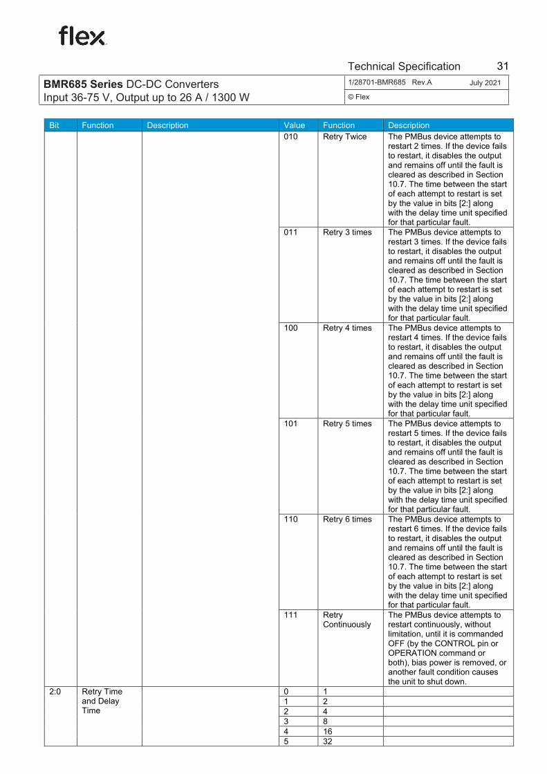
000 Do Not Retry A zero value for the Retry Setting means that the unit does not attempt to restart. The output remains disabled until the fault is cleared (Section 10.7).
001 Retry Once The PMBus device attempts to restart 1 time. If the device fails to restart, it disables the output and remains off until the fault is cleared as described in Section 10.7. The time between the start of each attempt to restart is set by the value in bits [2:] along with the delay time unit specified for that particular fault.
IOUT_CAL_OFFSET (0x39) Description: Sets the current-sense offset.
VOUT_OV_FAULT_LIMIT (0x40) Description: Output over voltage fault limit.
VOUT_OV_FAULT_RESPONSE (0x41) Description: Output over voltage fault response.
BMR685 Series DC-DC Converters Input 36-75 V, Output up to 26 A / 1300 W
1/28701-BMR685 Rev.A July 2021
© Flex
Technical Specification 30
PUBLIC
PRODUCT SPECIFICATION
10 (39) Prepared (Subject resp) No.
jidwwang Wenfa Wang 6/1301-BMR685XXXX/820 Approved (Document resp) Checked Date Rev
jidwwang Wenfa Wang 9/5/2020 A
Bit Function Description Value Function Description 010 Retry Twice The PMBus device attempts to
restart 2 times. If the device fails to restart, it disables the output and remains off until the fault is cleared as described in Section 10.7. The time between the start of each attempt to restart is set by the value in bits [2:] along with the delay time unit specified for that particular fault.
011 Retry 3 times The PMBus device attempts to restart 3 times. If the device fails to restart, it disables the output and remains off until the fault is cleared as described in Section 10.7. The time between the start of each attempt to restart is set by the value in bits [2:] along with the delay time unit specified for that particular fault.
100 Retry 4 times The PMBus device attempts to restart 4 times. If the device fails to restart, it disables the output and remains off until the fault is cleared as described in Section 10.7. The time between the start of each attempt to restart is set by the value in bits [2:] along with the delay time unit specified for that particular fault.
101 Retry 5 times The PMBus device attempts to restart 5 times. If the device fails to restart, it disables the output and remains off until the fault is cleared as described in Section 10.7. The time between the start of each attempt to restart is set by the value in bits [2:] along with the delay time unit specified for that particular fault.
110 Retry 6 times The PMBus device attempts to restart 6 times. If the device fails to restart, it disables the output and remains off until the fault is cleared as described in Section 10.7. The time between the start of each attempt to restart is set by the value in bits [2:] along with the delay time unit specified for that particular fault.
111 Retry Continuously
The PMBus device attempts to restart continuously, without limitation, until it is commanded OFF (by the CONTROL pin or OPERATION command or both), bias power is removed, or another fault condition causes the unit to shut down.
2:0 Retry Time and Delay Time
0 1 1 2 2 4 3 8 4 16 5 32
BMR685 Series DC-DC Converters Input 36-75 V, Output up to 26 A / 1300 W
1/28701-BMR685 Rev.A July 2021
© Flex
Technical Specification 31
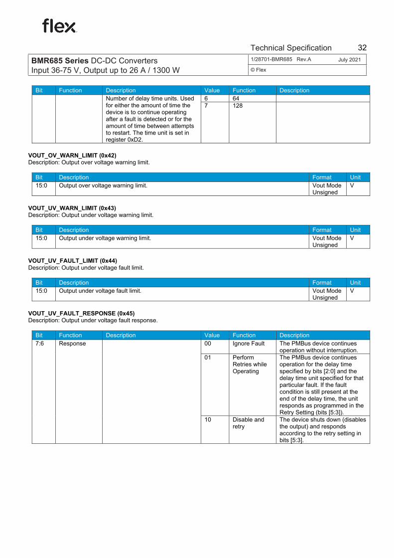
PUBLIC
PRODUCT SPECIFICATION
11 (39) Prepared (Subject resp) No.
jidwwang Wenfa Wang 6/1301-BMR685XXXX/820 Approved (Document resp) Checked Date Rev
jidwwang Wenfa Wang 9/5/2020 A
Bit Function Description Value Function Description Number of delay time units. Used for either the amount of time the device is to continue operating after a fault is detected or for the amount of time between attempts to restart. The time unit is set in register 0xD2.
6 64 7 128
Bit Description Format Unit 15:0 Output over voltage warning limit. Vout Mode
Unsigned V
Bit Description Format Unit 15:0 Output under voltage warning limit. Vout Mode
Unsigned V
Bit Description Format Unit 15:0 Output under voltage fault limit. Vout Mode
Unsigned V
Bit Function Description Value Function Description 7:6 Response 00 Ignore Fault The PMBus device continues
operation without interruption. 01 Perform
Retries while Operating
The PMBus device continues operation for the delay time specified by bits [2:0] and the delay time unit specified for that particular fault. If the fault condition is still present at the end of the delay time, the unit responds as programmed in the Retry Setting (bits [5:3]).
10 Disable and retry
The device shuts down (disables the output) and responds according to the retry setting in bits [5:3].
VOUT_OV_WARN_LIMIT (0x42) Description: Output over voltage warning limit.
VOUT_UV_WARN_LIMIT (0x43) Description: Output under voltage warning limit.
VOUT_UV_FAULT_LIMIT (0x44) Description: Output under voltage fault limit.
VOUT_UV_FAULT_RESPONSE (0x45) Description: Output under voltage fault response.
BMR685 Series DC-DC Converters Input 36-75 V, Output up to 26 A / 1300 W
1/28701-BMR685 Rev.A July 2021
© Flex
Technical Specification 32

PUBLIC
PRODUCT SPECIFICATION
12 (39) Prepared (Subject resp) No.
jidwwang Wenfa Wang 6/1301-BMR685XXXX/820 Approved (Document resp) Checked Date Rev
jidwwang Wenfa Wang 9/5/2020 A
Bit Function Description Value Function Description Describes the device interruption operation. 00b - The PMBus device continues operation without interruption. 01b - The PMBus device continues operation for the delay time specified by bits [2:0] and the delay time unit specified for that particular fault. If the fault condition condition is still present at the end of the delay time, the unit responds as programmed in the Retry Setting (bits [5:3]). 10b - The device shuts down (disables the output) and responds according to the Retry Setting in bits [5:3]. 11b - The device's output is disabled while the fault is present. Operation resumes and the output is enabled when the fault condition no longer exists.
11 Disable until Fault Cleared
A fault can cleared in several ways: The bit is individually cleared, The device receives a CLEAR_FAULTS command, a RESET signal (if one exists) is asserted, the output is commanded through the CTRL pin, the OPERATION command, or the combined action of the CTRL pin and OPERATION command, to turn off and then to turn back on, or Bias power is removed from the PMBus device.
5:3 Retries The device attempts to restart the number of times set by these bits. 000b means the device does not attempt a restart. 111b means the device attempts restarting continuously.
000 Do Not Retry A zero value for the Retry Setting means that the unit does not attempt to restart. The output remains disabled until the fault is cleared (Section 10.7).
001 Retry Once The PMBus device attempts to restart 1 time. If the device fails to restart, it disables the output and remains off until the fault is cleared as described in Section 10.7. The time between the start of each attempt to restart is set by the value in bits [2:] along with the delay time unit specified for that particular fault.
010 Retry Twice The PMBus device attempts to restart 2 times. If the device fails to restart, it disables the output and remains off until the fault is cleared as described in Section 10.7. The time between the start of each attempt to restart is set by the value in bits [2:] along with the delay time unit specified for that particular fault.
011 Retry 3 times The PMBus device attempts to restart 3 times. If the device fails to restart, it disables the output and remains off until the fault is cleared as described in Section 10.7. The time between the start of each attempt to restart is set by the value in bits [2:] along with the delay time unit specified for that particular fault.
BMR685 Series DC-DC Converters Input 36-75 V, Output up to 26 A / 1300 W
1/28701-BMR685 Rev.A July 2021
© Flex
Technical Specification 33
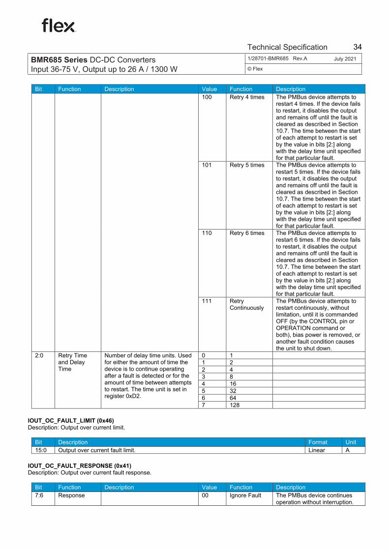
PUBLIC
PRODUCT SPECIFICATION
13 (39) Prepared (Subject resp) No.
jidwwang Wenfa Wang 6/1301-BMR685XXXX/820 Approved (Document resp) Checked Date Rev
jidwwang Wenfa Wang 9/5/2020 A
Bit Function Description Value Function Description 100 Retry 4 times The PMBus device attempts to
restart 4 times. If the device fails to restart, it disables the output and remains off until the fault is cleared as described in Section 10.7. The time between the start of each attempt to restart is set by the value in bits [2:] along with the delay time unit specified for that particular fault.
101 Retry 5 times The PMBus device attempts to restart 5 times. If the device fails to restart, it disables the output and remains off until the fault is cleared as described in Section 10.7. The time between the start of each attempt to restart is set by the value in bits [2:] along with the delay time unit specified for that particular fault.
110 Retry 6 times The PMBus device attempts to restart 6 times. If the device fails to restart, it disables the output and remains off until the fault is cleared as described in Section 10.7. The time between the start of each attempt to restart is set by the value in bits [2:] along with the delay time unit specified for that particular fault.
111 Retry Continuously
The PMBus device attempts to restart continuously, without limitation, until it is commanded OFF (by the CONTROL pin or OPERATION command or both), bias power is removed, or another fault condition causes the unit to shut down.
2:0 Retry Time and Delay Time
Number of delay time units. Used for either the amount of time the device is to continue operating after a fault is detected or for the amount of time between attempts to restart. The time unit is set in register 0xD2.
0 1 1 2 2 4 3 8 4 16 5 32 6 64 7 128
Bit Description Format Unit 15:0 Output over current fault limit. Linear A
Bit Function Description Value Function Description 7:6 Response 00 Ignore Fault The PMBus device continues
operation without interruption.
IOUT_OC_FAULT_LIMIT (0x46) Description: Output over current limit.
IOUT_OC_FAULT_RESPONSE (0x41) Description: Output over current fault response.
BMR685 Series DC-DC Converters Input 36-75 V, Output up to 26 A / 1300 W
1/28701-BMR685 Rev.A July 2021
© Flex
Technical Specification 34

PUBLIC
PRODUCT SPECIFICATION
14 (39) Prepared (Subject resp) No.
jidwwang Wenfa Wang 6/1301-BMR685XXXX/820 Approved (Document resp) Checked Date Rev
jidwwang Wenfa Wang 9/5/2020 A
Bit Function Description Value Function Description Describes the device interruption operation. 00b - The PMBus device continues operation without interruption. 01b - The PMBus device continues operation for the delay time specified by bits [2:0] and the delay time unit specified for that particular fault. If the fault condition condition is still present at the end of the delay time, the unit responds as programmed in the Retry Setting (bits [5:3]). 10b - The device shuts down (disables the output) and responds according to the Retry Setting in bits [5:3]. 11b - The device's output is disabled while the fault is present. Operation resumes and the output is enabled when the fault condition no longer exists.
01 Perform Retries while Operating
The PMBus device continues operation for the delay time specified by bits [2:0] and the delay time unit specified for that particular fault. If the fault condition is still present at the end of the delay time, the unit responds as programmed in the Retry Setting (bits [5:3]).
10 Disable and retry
The device shuts down (disables the output) and responds according to the retry setting in bits [5:3].
11 Disable until Fault Cleared
A fault can cleared in several ways: The bit is individually cleared, The device receives a CLEAR_FAULTS command, a RESET signal (if one exists) is asserted, the output is commanded through the CTRL pin, the OPERATION command, or the combined action of the CTRL pin and OPERATION command, to turn off and then to turn back on, or Bias power is removed from the PMBus device.
5:3 Retries The device attempts to restart the number of times set by these bits. 000b means the device does not attempt a restart. 111b means the device attempts restarting continuously.
000 Do Not Retry A zero value for the Retry Setting means that the unit does not attempt to restart. The output remains disabled until the fault is cleared (Section 10.7).
001 Retry Once The PMBus device attempts to restart 1 time. If the device fails to restart, it disables the output and remains off until the fault is cleared as described in Section 10.7. The time between the start of each attempt to restart is set by the value in bits [2:] along with the delay time unit specified for that particular fault.
010 Retry Twice The PMBus device attempts to restart 2 times. If the device fails to restart, it disables the output and remains off until the fault is cleared as described in Section 10.7. The time between the start of each attempt to restart is set by the value in bits [2:] along with the delay time unit specified for that particular fault.
011 Retry 3 times The PMBus device attempts to restart 3 times. If the device fails to restart, it disables the output and remains off until the fault is cleared as described in Section 10.7. The time between the start of each attempt to restart is set by the value in bits [2:] along with the delay time unit specified for that particular fault.
BMR685 Series DC-DC Converters Input 36-75 V, Output up to 26 A / 1300 W
1/28701-BMR685 Rev.A July 2021
© Flex
Technical Specification 35
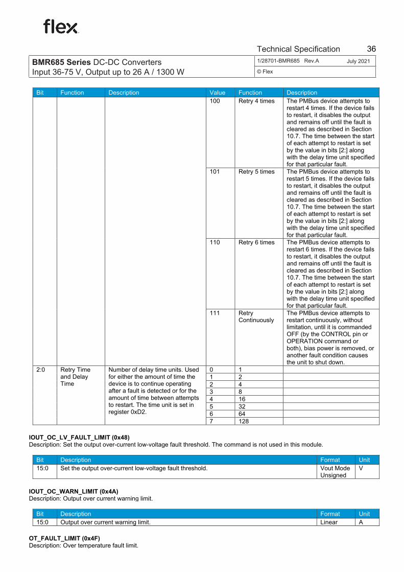
PUBLIC
PRODUCT SPECIFICATION
15 (39) Prepared (Subject resp) No.
jidwwang Wenfa Wang 6/1301-BMR685XXXX/820 Approved (Document resp) Checked Date Rev
jidwwang Wenfa Wang 9/5/2020 A
Bit Function Description Value Function Description 100 Retry 4 times The PMBus device attempts to
restart 4 times. If the device fails to restart, it disables the output and remains off until the fault is cleared as described in Section 10.7. The time between the start of each attempt to restart is set by the value in bits [2:] along with the delay time unit specified for that particular fault.
101 Retry 5 times The PMBus device attempts to restart 5 times. If the device fails to restart, it disables the output and remains off until the fault is cleared as described in Section 10.7. The time between the start of each attempt to restart is set by the value in bits [2:] along with the delay time unit specified for that particular fault.
110 Retry 6 times The PMBus device attempts to restart 6 times. If the device fails to restart, it disables the output and remains off until the fault is cleared as described in Section 10.7. The time between the start of each attempt to restart is set by the value in bits [2:] along with the delay time unit specified for that particular fault.
111 Retry Continuously
The PMBus device attempts to restart continuously, without limitation, until it is commanded OFF (by the CONTROL pin or OPERATION command or both), bias power is removed, or another fault condition causes the unit to shut down.
2:0 Retry Time and Delay Time
Number of delay time units. Used for either the amount of time the device is to continue operating after a fault is detected or for the amount of time between attempts to restart. The time unit is set in register 0xD2.
0 1 1 2 2 4 3 8 4 16 5 32 6 64 7 128
Bit Description Format Unit 15:0 Set the output over-current low-voltage fault threshold. Vout Mode
Unsigned V
Bit Description Format Unit 15:0 Output over current warning limit. Linear A
IOUT_OC_LV_FAULT_LIMIT (0x48) Description: Set the output over-current low-voltage fault threshold. The command is not used in this module.
IOUT_OC_WARN_LIMIT (0x4A) Description: Output over current warning limit.
OT_FAULT_LIMIT (0x4F) Description: Over temperature fault limit.
BMR685 Series DC-DC Converters Input 36-75 V, Output up to 26 A / 1300 W
1/28701-BMR685 Rev.A July 2021
© Flex
Technical Specification 36
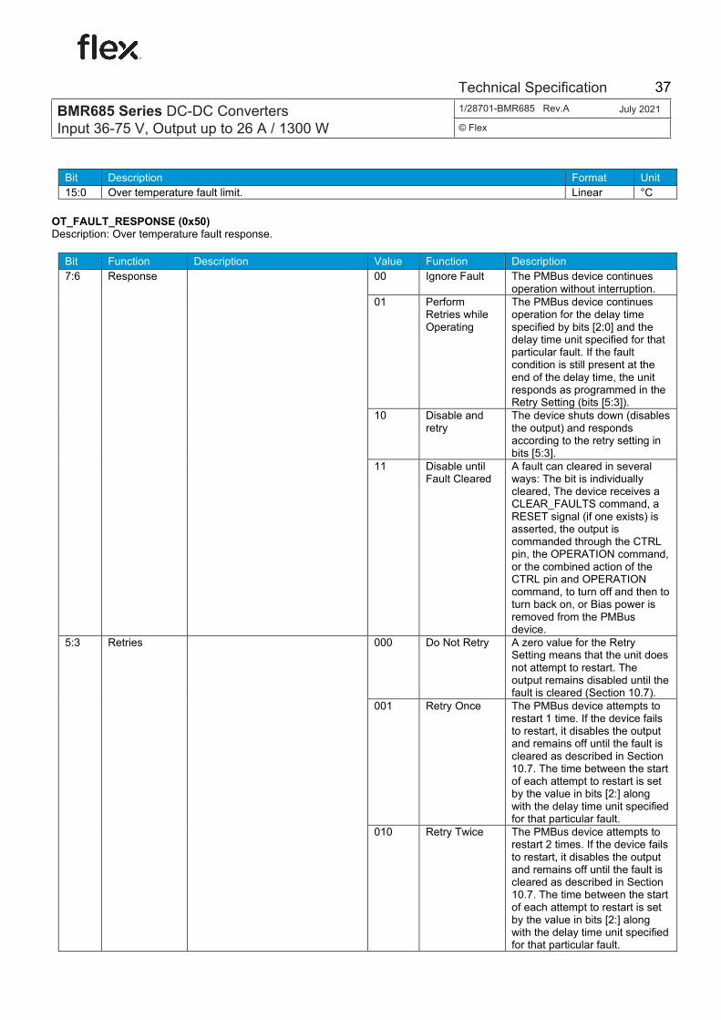
PUBLIC
PRODUCT SPECIFICATION
16 (39) Prepared (Subject resp) No.
jidwwang Wenfa Wang 6/1301-BMR685XXXX/820 Approved (Document resp) Checked Date Rev
jidwwang Wenfa Wang 9/5/2020 A
Bit Description Format Unit 15:0 Over temperature fault limit. Linear °C
Bit Function Description Value Function Description 7:6 Response 00 Ignore Fault The PMBus device continues
operation without interruption. 01 Perform
Retries while Operating
The PMBus device continues operation for the delay time specified by bits [2:0] and the delay time unit specified for that particular fault. If the fault condition is still present at the end of the delay time, the unit responds as programmed in the Retry Setting (bits [5:3]).
10 Disable and retry
The device shuts down (disables the output) and responds according to the retry setting in bits [5:3].
11 Disable until Fault Cleared
A fault can cleared in several ways: The bit is individually cleared, The device receives a CLEAR_FAULTS command, a RESET signal (if one exists) is asserted, the output is commanded through the CTRL pin, the OPERATION command, or the combined action of the CTRL pin and OPERATION command, to turn off and then to turn back on, or Bias power is removed from the PMBus device.
5:3 Retries 000 Do Not Retry A zero value for the Retry Setting means that the unit does not attempt to restart. The output remains disabled until the fault is cleared (Section 10.7).
001 Retry Once The PMBus device attempts to restart 1 time. If the device fails to restart, it disables the output and remains off until the fault is cleared as described in Section 10.7. The time between the start of each attempt to restart is set by the value in bits [2:] along with the delay time unit specified for that particular fault.
010 Retry Twice The PMBus device attempts to restart 2 times. If the device fails to restart, it disables the output and remains off until the fault is cleared as described in Section 10.7. The time between the start of each attempt to restart is set by the value in bits [2:] along with the delay time unit specified for that particular fault.
OT_FAULT_RESPONSE (0x50) Description: Over temperature fault response.
BMR685 Series DC-DC Converters Input 36-75 V, Output up to 26 A / 1300 W
1/28701-BMR685 Rev.A July 2021
© Flex
Technical Specification 37
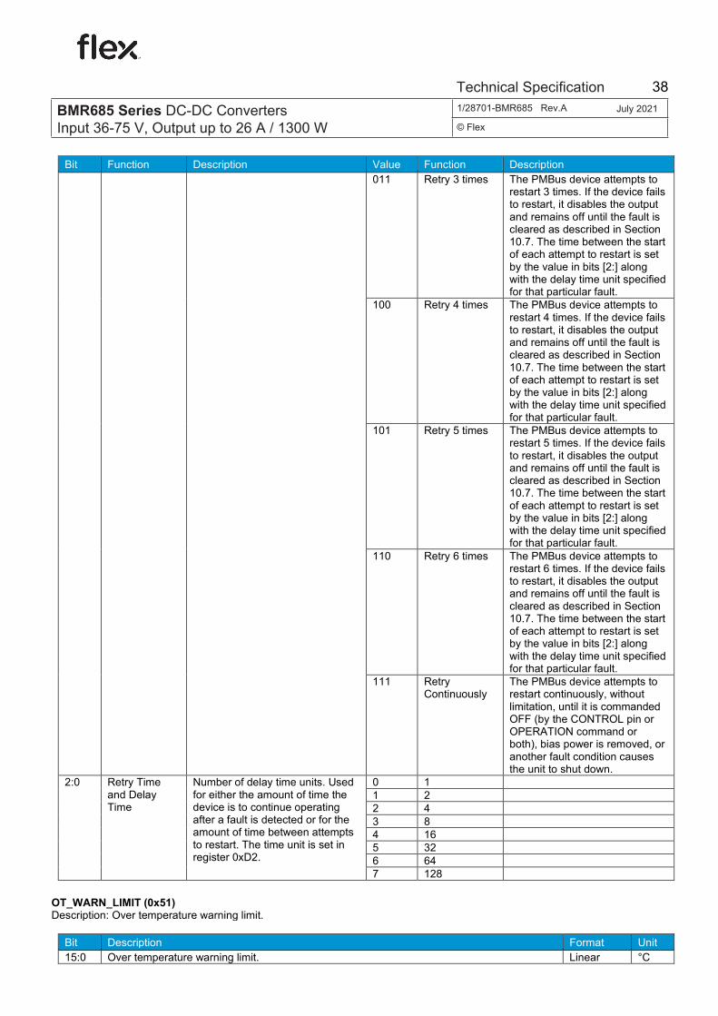
PUBLIC
PRODUCT SPECIFICATION
17 (39) Prepared (Subject resp) No.
jidwwang Wenfa Wang 6/1301-BMR685XXXX/820 Approved (Document resp) Checked Date Rev
jidwwang Wenfa Wang 9/5/2020 A
Bit Function Description Value Function Description 011 Retry 3 times The PMBus device attempts to
restart 3 times. If the device fails to restart, it disables the output and remains off until the fault is cleared as described in Section 10.7. The time between the start of each attempt to restart is set by the value in bits [2:] along with the delay time unit specified for that particular fault.
100 Retry 4 times The PMBus device attempts to restart 4 times. If the device fails to restart, it disables the output and remains off until the fault is cleared as described in Section 10.7. The time between the start of each attempt to restart is set by the value in bits [2:] along with the delay time unit specified for that particular fault.
101 Retry 5 times The PMBus device attempts to restart 5 times. If the device fails to restart, it disables the output and remains off until the fault is cleared as described in Section 10.7. The time between the start of each attempt to restart is set by the value in bits [2:] along with the delay time unit specified for that particular fault.
110 Retry 6 times The PMBus device attempts to restart 6 times. If the device fails to restart, it disables the output and remains off until the fault is cleared as described in Section 10.7. The time between the start of each attempt to restart is set by the value in bits [2:] along with the delay time unit specified for that particular fault.
111 Retry Continuously
The PMBus device attempts to restart continuously, without limitation, until it is commanded OFF (by the CONTROL pin or OPERATION command or both), bias power is removed, or another fault condition causes the unit to shut down.
2:0 Retry Time and Delay Time
Number of delay time units. Used for either the amount of time the device is to continue operating after a fault is detected or for the amount of time between attempts to restart. The time unit is set in register 0xD2.
0 1 1 2 2 4 3 8 4 16 5 32 6 64 7 128
Bit Description Format Unit 15:0 Over temperature warning limit. Linear °C
OT_WARN_LIMIT (0x51) Description: Over temperature warning limit.
BMR685 Series DC-DC Converters Input 36-75 V, Output up to 26 A / 1300 W
1/28701-BMR685 Rev.A July 2021
© Flex
Technical Specification 38

PUBLIC
PRODUCT SPECIFICATION
18 (39) Prepared (Subject resp) No.
jidwwang Wenfa Wang 6/1301-BMR685XXXX/820 Approved (Document resp) Checked Date Rev
jidwwang Wenfa Wang 9/5/2020 A
Bit Description Format Unit 15:0 Under temperature warning limit. Linear °C
Bit Description Format Unit 15:0 Under temperature fault limit. Linear °C
Bit Function Description Value Function Description 7:6 Response 00 Ignore Fault The PMBus device continues
operation without interruption. 01 Perform
Retries while Operating
The PMBus device continues operation for the delay time specified by bits [2:0] and the delay time unit specified for that particular fault. If the fault condition is still present at the end of the delay time, the unit responds as programmed in the Retry Setting (bits [5:3]).
10 Disable and retry
The device shuts down (disables the output) and responds according to the retry setting in bits [5:3].
11 Disable until Fault Cleared
A fault can cleared in several ways: The bit is individually cleared, The device receives a CLEAR_FAULTS command, a RESET signal (if one exists) is asserted, the output is commanded through the CTRL pin, the OPERATION command, or the combined action of the CTRL pin and OPERATION command, to turn off and then to turn back on, or Bias power is removed from the PMBus device.
5:3 Retries 000 Do Not Retry A zero value for the Retry Setting means that the unit does not attempt to restart. The output remains disabled until the fault is cleared (Section 10.7).
001 Retry Once The PMBus device attempts to restart 1 time. If the device fails to restart, it disables the output and remains off until the fault is cleared as described in Section 10.7. The time between the start of each attempt to restart is set by the value in bits [2:] along with the delay time unit specified for that particular fault.
UT_WARN_LIMIT (0x52) Description: Under temperature warning limit.
UT_FAULT_LIMIT (0x53) Description: Under temperature fault limit.
UT_FAULT_RESPONSE (0x54) Description: Under temperature fault response.
BMR685 Series DC-DC Converters Input 36-75 V, Output up to 26 A / 1300 W
1/28701-BMR685 Rev.A July 2021
© Flex
Technical Specification 39

PUBLIC
PRODUCT SPECIFICATION
19 (39) Prepared (Subject resp) No.
jidwwang Wenfa Wang 6/1301-BMR685XXXX/820 Approved (Document resp) Checked Date Rev
jidwwang Wenfa Wang 9/5/2020 A
Bit Function Description Value Function Description 010 Retry Twice The PMBus device attempts to
restart 2 times. If the device fails to restart, it disables the output and remains off until the fault is cleared as described in Section 10.7. The time between the start of each attempt to restart is set by the value in bits [2:] along with the delay time unit specified for that particular fault.
011 Retry 3 times The PMBus device attempts to restart 3 times. If the device fails to restart, it disables the output and remains off until the fault is cleared as described in Section 10.7. The time between the start of each attempt to restart is set by the value in bits [2:] along with the delay time unit specified for that particular fault.
100 Retry 4 times The PMBus device attempts to restart 4 times. If the device fails to restart, it disables the output and remains off until the fault is cleared as described in Section 10.7. The time between the start of each attempt to restart is set by the value in bits [2:] along with the delay time unit specified for that particular fault.
101 Retry 5 times The PMBus device attempts to restart 5 times. If the device fails to restart, it disables the output and remains off until the fault is cleared as described in Section 10.7. The time between the start of each attempt to restart is set by the value in bits [2:] along with the delay time unit specified for that particular fault.
110 Retry 6 times The PMBus device attempts to restart 6 times. If the device fails to restart, it disables the output and remains off until the fault is cleared as described in Section 10.7. The time between the start of each attempt to restart is set by the value in bits [2:] along with the delay time unit specified for that particular fault.
111 Retry Continuously
The PMBus device attempts to restart continuously, without limitation, until it is commanded OFF (by the CONTROL pin or OPERATION command or both), bias power is removed, or another fault condition causes the unit to shut down.
2:0 Retry Time and Delay Time
0 1 1 2 2 4 3 8 4 16 5 32
BMR685 Series DC-DC Converters Input 36-75 V, Output up to 26 A / 1300 W
1/28701-BMR685 Rev.A July 2021
© Flex
Technical Specification 40

PUBLIC
PRODUCT SPECIFICATION
20 (39) Prepared (Subject resp) No.
jidwwang Wenfa Wang 6/1301-BMR685XXXX/820 Approved (Document resp) Checked Date Rev
jidwwang Wenfa Wang 9/5/2020 A
Bit Function Description Value Function Description Number of delay time units. Used for either the amount of time the device is to continue operating after a fault is detected or for the amount of time between attempts to restart. The time unit is set in register 0xD2.
6 64 7 128
Bit Description Format Unit 15:0 Input over voltage fault limit. Linear V
Bit Function Description Value Function Description 7:6 Response 00 Ignore Fault The PMBus device continues
operation without interruption. 01 Perform
Retries while Operating
The PMBus device continues operation for the delay time specified by bits [2:0] and the delay time unit specified for that particular fault. If the fault condition is still present at the end of the delay time, the unit responds as programmed in the Retry Setting (bits [5:3]).
10 Disable and retry
The device shuts down (disables the output) and responds according to the retry setting in bits [5:3].
11 Disable until Fault Cleared
A fault can cleared in several ways: The bit is individually cleared, The device receives a CLEAR_FAULTS command, a RESET signal (if one exists) is asserted, the output is commanded through the CTRL pin, the OPERATION command, or the combined action of the CTRL pin and OPERATION command, to turn off and then to turn back on, or Bias power is removed from the PMBus device.
5:3 Retries 000 Do Not Retry A zero value for the Retry Setting means that the unit does not attempt to restart. The output remains disabled until the fault is cleared (Section 10.7).
001 Retry Once The PMBus device attempts to restart 1 time. If the device fails to restart, it disables the output and remains off until the fault is cleared as described in Section 10.7. The time between the start of each attempt to restart is set by the value in bits [2:] along with the delay time unit specified for that particular fault.
VIN_OV_FAULT_LIMIT (0x55) Description: Input over voltage fault limit.
VIN_OV_FAULT_RESPONSE (0x56) Description: Input over voltage fault response.
BMR685 Series DC-DC Converters Input 36-75 V, Output up to 26 A / 1300 W
1/28701-BMR685 Rev.A July 2021
© Flex
Technical Specification 41

PUBLIC
PRODUCT SPECIFICATION
21 (39) Prepared (Subject resp) No.
jidwwang Wenfa Wang 6/1301-BMR685XXXX/820 Approved (Document resp) Checked Date Rev
jidwwang Wenfa Wang 9/5/2020 A
Bit Function Description Value Function Description 010 Retry Twice The PMBus device attempts to
restart 2 times. If the device fails to restart, it disables the output and remains off until the fault is cleared as described in Section 10.7. The time between the start of each attempt to restart is set by the value in bits [2:] along with the delay time unit specified for that particular fault.
011 Retry 3 times The PMBus device attempts to restart 3 times. If the device fails to restart, it disables the output and remains off until the fault is cleared as described in Section 10.7. The time between the start of each attempt to restart is set by the value in bits [2:] along with the delay time unit specified for that particular fault.
100 Retry 4 times The PMBus device attempts to restart 4 times. If the device fails to restart, it disables the output and remains off until the fault is cleared as described in Section 10.7. The time between the start of each attempt to restart is set by the value in bits [2:] along with the delay time unit specified for that particular fault.
101 Retry 5 times The PMBus device attempts to restart 5 times. If the device fails to restart, it disables the output and remains off until the fault is cleared as described in Section 10.7. The time between the start of each attempt to restart is set by the value in bits [2:] along with the delay time unit specified for that particular fault.
110 Retry 6 times The PMBus device attempts to restart 6 times. If the device fails to restart, it disables the output and remains off until the fault is cleared as described in Section 10.7. The time between the start of each attempt to restart is set by the value in bits [2:] along with the delay time unit specified for that particular fault.
111 Retry Continuously
The PMBus device attempts to restart continuously, without limitation, until it is commanded OFF (by the CONTROL pin or OPERATION command or both), bias power is removed, or another fault condition causes the unit to shut down.
2:0 Retry Time and Delay Time
0 1 1 2 2 4 3 8 4 16 5 32
BMR685 Series DC-DC Converters Input 36-75 V, Output up to 26 A / 1300 W
1/28701-BMR685 Rev.A July 2021
© Flex
Technical Specification 42

PUBLIC
PRODUCT SPECIFICATION
22 (39) Prepared (Subject resp) No.
jidwwang Wenfa Wang 6/1301-BMR685XXXX/820 Approved (Document resp) Checked Date Rev
jidwwang Wenfa Wang 9/5/2020 A
Bit Function Description Value Function Description Number of delay time units. Used for either the amount of time the device is to continue operating after a fault is detected or for the amount of time between attempts to restart. The time unit is set in register 0xD2.
6 64 7 128
Bit Description Format Unit 15:0 Input over voltage warning limit. Linear V
Bit Description Format Unit 15:0 Input under voltage warning limit and/or HRR threshold. Linear V
Bit Description Format Unit 15:0 Input under voltage fault limit. Linear V
Bit Function Description Value Function Description 7:6 Response 00 Ignore Fault The PMBus device continues
operation without interruption. 01 Perform
Retries while Operating
The PMBus device continues operation for the delay time specified by bits [2:0] and the delay time unit specified for that particular fault. If the fault condition is still present at the end of the delay time, the unit responds as programmed in the Retry Setting (bits [5:3]).
10 Disable and retry
The device shuts down (disables the output) and responds according to the retry setting in bits [5:3].
11 Disable until Fault Cleared
A fault can cleared in several ways: The bit is individually cleared, The device receives a CLEAR_FAULTS command, a RESET signal (if one exists) is asserted, the output is commanded through the CTRL pin, the OPERATION command, or the combined action of the CTRL pin and OPERATION command, to turn off and then to turn back on, or Bias power is removed from the PMBus device.
VIN_OV_WARN_LIMIT (0x57) Description: Input over voltage warning limit.
VIN_UV_WARN_LIMIT (0x58) Description: Input under voltage warning limit. This command set also the input voltage threshold for the HRR function (Hybrid Ratio Regulation). The HRR function is enabled with command MFR_SPECIAL_OPTIONS (0xE0).
VIN_UV_FAULT_LIMIT (0x59) Description: Input under voltage fault limit.
VIN_UV_FAULT_RESPONSE (0x5A) Description: Input under voltage fault response.
BMR685 Series DC-DC Converters Input 36-75 V, Output up to 26 A / 1300 W
1/28701-BMR685 Rev.A July 2021
© Flex
Technical Specification 43

PUBLIC
PRODUCT SPECIFICATION
23 (39) Prepared (Subject resp) No.
jidwwang Wenfa Wang 6/1301-BMR685XXXX/820 Approved (Document resp) Checked Date Rev
jidwwang Wenfa Wang 9/5/2020 A
Bit Function Description Value Function Description 5:3 Retries 000 Do Not Retry A zero value for the Retry
Setting means that the unit does not attempt to restart. The output remains disabled until the fault is cleared (Section 10.7).
001 Retry Once The PMBus device attempts to restart 1 time. If the device fails to restart, it disables the output and remains off until the fault is cleared as described in Section 10.7. The time between the start of each attempt to restart is set by the value in bits [2:] along with the delay time unit specified for that particular fault.
010 Retry Twice The PMBus device attempts to restart 2 times. If the device fails to restart, it disables the output and remains off until the fault is cleared as described in Section 10.7. The time between the start of each attempt to restart is set by the value in bits [2:] along with the delay time unit specified for that particular fault.
011 Retry 3 times The PMBus device attempts to restart 3 times. If the device fails to restart, it disables the output and remains off until the fault is cleared as described in Section 10.7. The time between the start of each attempt to restart is set by the value in bits [2:] along with the delay time unit specified for that particular fault.
100 Retry 4 times The PMBus device attempts to restart 4 times. If the device fails to restart, it disables the output and remains off until the fault is cleared as described in Section 10.7. The time between the start of each attempt to restart is set by the value in bits [2:] along with the delay time unit specified for that particular fault.
101 Retry 5 times The PMBus device attempts to restart 5 times. If the device fails to restart, it disables the output and remains off until the fault is cleared as described in Section 10.7. The time between the start of each attempt to restart is set by the value in bits [2:] along with the delay time unit specified for that particular fault.
BMR685 Series DC-DC Converters Input 36-75 V, Output up to 26 A / 1300 W
1/28701-BMR685 Rev.A July 2021
© Flex
Technical Specification 44
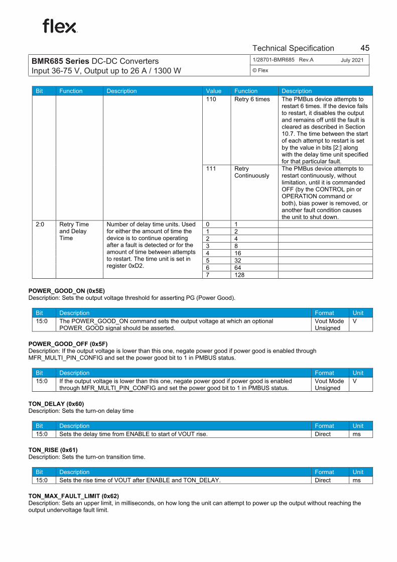
PUBLIC
PRODUCT SPECIFICATION
24 (39) Prepared (Subject resp) No.
jidwwang Wenfa Wang 6/1301-BMR685XXXX/820 Approved (Document resp) Checked Date Rev
jidwwang Wenfa Wang 9/5/2020 A
Bit Function Description Value Function Description 110 Retry 6 times The PMBus device attempts to
restart 6 times. If the device fails to restart, it disables the output and remains off until the fault is cleared as described in Section 10.7. The time between the start of each attempt to restart is set by the value in bits [2:] along with the delay time unit specified for that particular fault.
111 Retry Continuously
The PMBus device attempts to restart continuously, without limitation, until it is commanded OFF (by the CONTROL pin or OPERATION command or both), bias power is removed, or another fault condition causes the unit to shut down.
2:0 Retry Time and Delay Time
Number of delay time units. Used for either the amount of time the device is to continue operating after a fault is detected or for the amount of time between attempts to restart. The time unit is set in register 0xD2.
0 1 1 2 2 4 3 8 4 16 5 32 6 64 7 128
Bit Description Format Unit 15:0 The POWER_GOOD_ON command sets the output voltage at which an optional
POWER_GOOD signal should be asserted. Vout Mode Unsigned
V
Bit Description Format Unit 15:0 If the output voltage is lower than this one, negate power good if power good is enabled
through MFR_MULTI_PIN_CONFIG and set the power good bit to 1 in PMBUS status. Vout Mode Unsigned
V
Bit Description Format Unit 15:0 Sets the delay time from ENABLE to start of VOUT rise. Direct ms
Bit Description Format Unit 15:0 Sets the rise time of VOUT after ENABLE and TON_DELAY. Direct ms
POWER_GOOD_ON (0x5E) Description: Sets the output voltage threshold for asserting PG (Power Good).
POWER_GOOD_OFF (0x5F) Description: If the output voltage is lower than this one, negate power good if power good is enabled through MFR_MULTI_PIN_CONFIG and set the power good bit to 1 in PMBUS status.
TON_DELAY (0x60) Description: Sets the turn-on delay time
TON_RISE (0x61) Description: Sets the turn-on transition time.
TON_MAX_FAULT_LIMIT (0x62) Description: Sets an upper limit, in milliseconds, on how long the unit can attempt to power up the output without reaching the output undervoltage fault limit.
BMR685 Series DC-DC Converters Input 36-75 V, Output up to 26 A / 1300 W
1/28701-BMR685 Rev.A July 2021
© Flex
Technical Specification 45

PUBLIC
PRODUCT SPECIFICATION
25 (39) Prepared (Subject resp) No.
jidwwang Wenfa Wang 6/1301-BMR685XXXX/820 Approved (Document resp) Checked Date Rev
jidwwang Wenfa Wang 9/5/2020 A
Bit Description Format Unit 15:0 A value of 0 milliseconds means that there is no limit and that the unit can attempt to bring up
the output voltage indefinitely. Direct ms
Bit Function Description Value Function Description 7:6 Response 00 Ignore Fault The PMBus device continues
operation without interruption. 01 Perform
Retries while Operating
The PMBus device continues operation for the delay time specified by bits [2:0] and the delay time unit specified for that particular fault. If the fault condition is still present at the end of the delay time, the unit responds as programmed in the Retry Setting (bits [5:3]).
10 Disable and retry
The device shuts down (disables the output) and responds according to the retry setting in bits [5:3].
11 Disable until Fault Cleared
A fault can cleared in several ways: The bit is individually cleared, The device receives a CLEAR_FAULTS command, a RESET signal (if one exists) is asserted, the output is commanded through the CTRL pin, the OPERATION command, or the combined action of the CTRL pin and OPERATION command, to turn off and then to turn back on, or Bias power is removed from the PMBus device.
5:3 Retries 000 Do Not Retry A zero value for the Retry Setting means that the unit does not attempt to restart. The output remains disabled until the fault is cleared (Section 10.7).
001 Retry Once The PMBus device attempts to restart 1 time. If the device fails to restart, it disables the output and remains off until the fault is cleared as described in Section 10.7. The time between the start of each attempt to restart is set by the value in bits [2:] along with the delay time unit specified for that particular fault.
010 Retry Twice The PMBus device attempts to restart 2 times. If the device fails to restart, it disables the output and remains off until the fault is cleared as described in Section 10.7. The time between the start of each attempt to restart is set by the value in bits [2:] along with the delay time unit specified for that particular fault.
TON_MAX_FAULT_RESPONSE (0x63) Description: Only some of the response types are supported.
BMR685 Series DC-DC Converters Input 36-75 V, Output up to 26 A / 1300 W
1/28701-BMR685 Rev.A July 2021
© Flex
Technical Specification 46

PUBLIC
PRODUCT SPECIFICATION
26 (39) Prepared (Subject resp) No.
jidwwang Wenfa Wang 6/1301-BMR685XXXX/820 Approved (Document resp) Checked Date Rev
jidwwang Wenfa Wang 9/5/2020 A
Bit Function Description Value Function Description 011 Retry 3 times The PMBus device attempts to
restart 3 times. If the device fails to restart, it disables the output and remains off until the fault is cleared as described in Section 10.7. The time between the start of each attempt to restart is set by the value in bits [2:] along with the delay time unit specified for that particular fault.
100 Retry 4 times The PMBus device attempts to restart 4 times. If the device fails to restart, it disables the output and remains off until the fault is cleared as described in Section 10.7. The time between the start of each attempt to restart is set by the value in bits [2:] along with the delay time unit specified for that particular fault.
101 Retry 5 times The PMBus device attempts to restart 5 times. If the device fails to restart, it disables the output and remains off until the fault is cleared as described in Section 10.7. The time between the start of each attempt to restart is set by the value in bits [2:] along with the delay time unit specified for that particular fault.
110 Retry 6 times The PMBus device attempts to restart 6 times. If the device fails to restart, it disables the output and remains off until the fault is cleared as described in Section 10.7. The time between the start of each attempt to restart is set by the value in bits [2:] along with the delay time unit specified for that particular fault.
111 Retry Continuously
The PMBus device attempts to restart continuously, without limitation, until it is commanded OFF (by the CONTROL pin or OPERATION command or both), bias power is removed, or another fault condition causes the unit to shut down.
2:0 Retry Time and Delay Time
Number of delay time units. Used for either the amount of time the device is to continue operating after a fault is detected or for the amount of time between attempts to restart. The time unit is set in register 0xD2. TON_MAX_FAULT_RESPONSE time unit is referenced to VOUT FAULT time unit.
0 1 1 2 2 4 3 8 4 16 5 32 6 64 7 128
TOFF_DELAY (0x64) Description: Sets the turn-off delay.
BMR685 Series DC-DC Converters Input 36-75 V, Output up to 26 A / 1300 W
1/28701-BMR685 Rev.A July 2021
© Flex
Technical Specification 47
PUBLIC
PRODUCT SPECIFICATION
27 (39) Prepared (Subject resp) No.
jidwwang Wenfa Wang 6/1301-BMR685XXXX/820 Approved (Document resp) Checked Date Rev
jidwwang Wenfa Wang 9/5/2020 A
Bit Description Format Unit 15:0 Sets the delay time from DISABLE to start of VOUT fall. Direct ms
Bit Description Format Unit 15:0 Sets the fall time for VOUT after DISABLE and TOFF_DELAY. Direct ms
Bit Description Format Unit 15:0 Direct ms
Bit Function Description Value Description 6 Off This bit is asserted if the unit is not providing power
to the output, regardless of the reason, including simply not being enabled.
0 No fault 1 Fault
5 Vout Overvoltage Fault
An output overvoltage fault has occurred. 0 No fault 1 Fault
4 Iout Overcurrent Fault An output overcurrent fault has occurred. 0 No fault 1 Fault
3 Vin Undervoltage Fault
An input undervoltage fault has occurred. 0 No fault 1 Fault
2 Temperature A temperature fault or warning has occurred. 0 No fault 1 Fault
1 Communication/Logic A communications, memory or logic fault has occurred.
0 No fault 1 Fault
0 None of the Above A fault or warning not listed in bits [7:1] has occured. 0 No fault 1 Fault
Bit Function Description Value Description 15 Vout An output voltage fault or warning has occurred. 0 No fault
1 Fault 14 Iout/Pout An output current or output power fault or warning
has occurred. 0 No Fault. 1 Fault.
13 Input An input voltage, input current, or input power fault or warning has occurred.
0 No Fault. 1 Fault.
11 Power-Good The Power-Good signal, if present, is negated. 0 No Fault. 1 Fault.
6 Off This bit is asserted if the unit is not providing power to the output, regardless of the reason, including simply not being enabled.
0 No fault 1 Fault
5 Vout Overvoltage Fault
An output overvoltage fault has occurred. 0 No Fault. 1 Fault.
4 Iout Overcurrent Fault An output overcurrent fault has occurred. 0 No Fault. 1 Fault.
3 Vin Undervoltage Fault
An input undervoltage fault has occurred. 0 No Fault. 1 Fault.
2 Temperature A temperature fault or warning has occurred. 0 No Fault. 1 Fault.
1 Communication/Logic A communications, memory or logic fault has occurred.
0 No fault. 1 Fault.
TOFF_FALL (0x65) Description: Sets the turn-off transition time.
TOFF_MAX_WARN_LIMIT (0x66) Description: Sets an upper limit, in milliseconds, on how long the unit can attempt to power down the output without reaching 12.5% of the output voltage programmed at the time the unit is turned off.
STATUS_BYTE (0x78) Description: Returns a brief fault/warning status byte.
STATUS_WORD (0x79) Description: Returns an extended fault/warning status byte.
BMR685 Series DC-DC Converters Input 36-75 V, Output up to 26 A / 1300 W
1/28701-BMR685 Rev.A July 2021
© Flex
Technical Specification 48

PUBLIC
PRODUCT SPECIFICATION
28 (39) Prepared (Subject resp) No.
jidwwang Wenfa Wang 6/1301-BMR685XXXX/820 Approved (Document resp) Checked Date Rev
jidwwang Wenfa Wang 9/5/2020 A
Bit Function Description Value Description 0 None of the Above A fault or warning not listed in bits [7:1] has occured. 0 No fault.
1 Fault.
Bit Function Description Value Description 7 Vout Overvoltage
Fault Vout Overvoltage Fault. 0 No Fault.
1 Fault. 6 Vout Overvoltage
Warning Vout Overvoltage Warning. 0 No Warning.
1 Warning. 5 Vout Undervoltage
Warning Vout Undervoltage Warning. 0 No Warning.
1 Warning. 4 Vout Undervoltage
Fault Vout Undervoltage Fault. 0 No Fault.
1 Fault. 3 Vout Max Warning Vout Max Warning (An attempt has been made to
set the output voltage to value higher than allowed by the Vout Max command (Section 13.5).
0 No Warning. 1 Warning.
2 Ton Max Fault Ton-Max Fault. 0 No Fault 1 Fault.
1 Toff Max Warning Toff Max Warning. 0 No Warning. 1 Warning.
Bit Function Description Value Description 7 Iout Overcurrent Fault Iout Overcurrent Fault. 0 No Fault.
1 Fault. 6 Iout Overcurrent And
Low Voltage Fault Iout Overcurrent and low voltage fault. 0 No Fault.
1 Fault. 5 Iout Over Current
Warning Iout Overcurrent Warning. 0 No Warning.
1 Warning. 4 Iout Undercurrent
Fault Iout Undercurrent Fault. 0 No Fault.
1 Fault.
Bit Function Description Value Description 7 Vin Overvoltage Fault Vin Overvoltage Fault. 0 No Fault.
1 Fault. 6 Vin Overvoltage
Warning VIN Overvoltage Warning. 0 No Warning.
1 Warning. 5 Vin Undervoltage
Warning Vin Undervoltage Warning. 0 No Warning.
1 Warning. 4 Vin Undervoltage
Fault Vin Undervoltage Fault. 0 No Fault.
1 Fault. 3 Insufficient Vin Asserted when either the input voltage has never
exceeded the input turn-on threshold Vin-On, or if the unit did start, the input voltage decreased below the turn-off threshold.
0 No Insuffient VIN encountered yet.
1 Insufficient Unit is off.
Bit Function Description Value Description 7 Overtemperature
Fault Overtemperature Fault. 0 No Fault.
1 Fault. 6 Overtemperature Warning. 0 No Warning.
STATUS_VOUT (0x7A) Description: Returns Vout-related fault/warning status bits.
STATUS_IOUT (0x7B) Description: Returns Iout-related fault/warning status bits.
STATUS_INPUT (0x7C) Description: Returns VIN/IIN-related fault/warning status bits.
STATUS_TEMPERATURE (0x7D) Description: Returns the temperature-related fault/warning status bits
BMR685 Series DC-DC Converters Input 36-75 V, Output up to 26 A / 1300 W
1/28701-BMR685 Rev.A July 2021
© Flex
Technical Specification 49
PUBLIC
PRODUCT SPECIFICATION
29 (39) Prepared (Subject resp) No.
jidwwang Wenfa Wang 6/1301-BMR685XXXX/820 Approved (Document resp) Checked Date Rev
jidwwang Wenfa Wang 9/5/2020 A
Bit Function Description Value Description Overtemperature Warning
1 Warning.
5 Undertemperature Warning
Undertemperature Warning. 0 No Warning. 1 Warning.
4 Undertemerature Fault
Undertemperature Fault. 0 No Fault. 1 Fault.
Bit Function Description Value Description 7 Invalid Or
Unsupported Command Received
Invalid Or Unsupported Command Received. 0 No Invalid Command Received.
1 Invalid Command Received.
6 Invalid Or Unsupported Data Received
Invalid Or Unsupported Data Received. 0 No Invalid Data Received.
1 Invalid Data Received. 5 Packet Error Check
Failed Packet Error Check Failed. 0 No Failure.
1 Failure. 4 Memory Fault
Detected Memory Fault Detected. 0 No Fault.
1 Fault. 1 Other Communication
Fault A communication fault other than the ones listed in this table has occurred.
0 No Fault. 1 Fault.
0 Memory Or Logic Fault
Other Memory Or Logic Fault has occurred. 0 No Fault. 1 Fault.
Bit Description Format Unit 15:0 Returns the input voltage reading. Linear V
Bit Description Format Unit 15:0 Returns the measured output voltage. Vout Mode
Unsigned V
Bit Description Format Unit 15:0 The device will NACK this command when not enabled and not in the USER_CONFIG
monitor mode. Linear A
Bit Description Format Unit 15:0 Linear °C
Bit Description Format Unit 15:0 Linear °C
STATUS_CML (0x7E) Description: Returns Communication/Logic/Memory-related fault/warning status bits.
READ_VIN (0x88) Description: Returns the measured input voltage.
READ_VOUT (0x8B) Description: Returns the measured output voltage.
READ_IOUT (0x8C) Description: Returns the measured output current.
READ_TEMPERATURE_1 (0x8D) Description: Returns the measured temperature (internal).
READ_TEMPERATURE_2 (0x8E) Description: Returns the measured temperature (internal).
BMR685 Series DC-DC Converters Input 36-75 V, Output up to 26 A / 1300 W
1/28701-BMR685 Rev.A July 2021
© Flex
Technical Specification 50

PUBLIC
PRODUCT SPECIFICATION
30 (39) Prepared (Subject resp) No.
jidwwang Wenfa Wang 6/1301-BMR685XXXX/820 Approved (Document resp) Checked Date Rev
jidwwang Wenfa Wang 9/5/2020 A
Bit Description Format Unit 15:0 Returns the target duty cycle during the ENABLE state. The device will NACK this command
when not enabled and not in the USER_CONFIG monitor mode. Linear %
Bit Description Format Unit 15:0 Returns the measured operating switch frequency. The device will NACK this command
when not enabled and not in the USER_CONFIG monitor mode. Direct kHz
Bit Function Description Value Function Description 7:4 Part I Revision Part I Revision. 0x0 1.0 Part I Revision 1.0.
0x1 1.1 Part I Revision 1.1. 0x2 1.2 Part I Revision 1.2. 0x3 1.3 Part I Revision 1.3.
3:0 Part II Revision
Part II Revision. 0x0 1.0 Part II Revision 1.0. 0x1 1.1 Part II Revision 1.1. 0x2 1.2 Part II Revision 1.2. 0x3 1.3 Part II Revision 1.3.
Bit Description Format 95:0 Maximum of 12 characters. ASCII
Bit Description Format 159:0 Maximum of 20 characters. ASCII
Bit Description Format 95:0 Maximum of 12 characters. ASCII
Bit Description Format 95:0 Maximum of 12 characters. ASCII
Bit Description Format 95:0 Maximum of 12 characters. ASCII
READ_DUTY_CYCLE (0x94) Description: Returns the measured duty cycle in percent.
READ_FREQUENCY (0x95) Description: Returns the measured SYNC frequency.
PMBUS_REVISION (0x98) Description: Returns the PMBus revision number for this device.
MFR_ID (0x99) Description: Sets the Manufacturers ID
MFR_MODEL (0x9A) Description: Sets the MFR MODEL string.
MFR_REVISION (0x9B) Description: Sets the MFR revision string.
MFR_LOCATION (0x9C) Description: Sets the MFR location string.
MFR_DATE (0x9D) Description: This command returns the date the regulator was manufactured.
MFR_SERIAL (0x9E) Description: This command returns a string of 13 characters and numbers that provides a unique identification of the regulator.
BMR685 Series DC-DC Converters Input 36-75 V, Output up to 26 A / 1300 W
1/28701-BMR685 Rev.A July 2021
© Flex
Technical Specification 51
PUBLIC
PRODUCT SPECIFICATION
31 (39) Prepared (Subject resp) No.
jidwwang Wenfa Wang 6/1301-BMR685XXXX/820 Approved (Document resp) Checked Date Rev
jidwwang Wenfa Wang 9/5/2020 A
Bit Description Format 159:0 Maximum of 20 characters. ASCII
Bit Description Format 127:0 16 bytes of user data. ASCII
Bit Function Description Value Function Description 7:6 Response 00 Ignore Fault The PMBus device continues
operation without interruption. 01 Perform
Retries while Operating
The PMBus device continues operation for the delay time specified by bits [2:0] and the delay time unit specified for that particular fault. If the fault condition is still present at the end of the delay time, the unit responds as programmed in the Retry Setting (bits [5:3]).
10 Disable and retry
The device shuts down (disables the output) and responds according to the retry setting in bits [5:3].
11 Disable until Fault Cleared
A fault can cleared in several ways: The bit is individually cleared, The device receives a CLEAR_FAULTS command, a RESET signal (if one exists) is asserted, the output is commanded through the CTRL pin, the OPERATION command, or the combined action of the CTRL pin and OPERATION command, to turn off and then to turn back on, or Bias power is removed from the PMBus device.
5:3 Retries 000 Do Not Retry A zero value for the Retry Setting means that the unit does not attempt to restart. The output remains disabled until the fault is cleared (Section 10.7).
001 Retry Once The PMBus device attempts to restart 1 time. If the device fails to restart, it disables the output and remains off until the fault is cleared as described in Section 10.7. The time between the start of each attempt to restart is set by the value in bits [2:] along with the delay time unit specified for that particular fault.
USER_DATA_00 (0xB0) Description: User data
MFR_VIN_OV_WARN_RESPONSE (0xC4) Description: Input over voltage Warn response.
BMR685 Series DC-DC Converters Input 36-75 V, Output up to 26 A / 1300 W
1/28701-BMR685 Rev.A July 2021
© Flex
Technical Specification 52

PUBLIC
PRODUCT SPECIFICATION
32 (39) Prepared (Subject resp) No.
jidwwang Wenfa Wang 6/1301-BMR685XXXX/820 Approved (Document resp) Checked Date Rev
jidwwang Wenfa Wang 9/5/2020 A
Bit Function Description Value Function Description 010 Retry Twice The PMBus device attempts to
restart 2 times. If the device fails to restart, it disables the output and remains off until the fault is cleared as described in Section 10.7. The time between the start of each attempt to restart is set by the value in bits [2:] along with the delay time unit specified for that particular fault.
011 Retry 3 times The PMBus device attempts to restart 3 times. If the device fails to restart, it disables the output and remains off until the fault is cleared as described in Section 10.7. The time between the start of each attempt to restart is set by the value in bits [2:] along with the delay time unit specified for that particular fault.
100 Retry 4 times The PMBus device attempts to restart 4 times. If the device fails to restart, it disables the output and remains off until the fault is cleared as described in Section 10.7. The time between the start of each attempt to restart is set by the value in bits [2:] along with the delay time unit specified for that particular fault.
101 Retry 5 times The PMBus device attempts to restart 5 times. If the device fails to restart, it disables the output and remains off until the fault is cleared as described in Section 10.7. The time between the start of each attempt to restart is set by the value in bits [2:] along with the delay time unit specified for that particular fault.
110 Retry 6 times The PMBus device attempts to restart 6 times. If the device fails to restart, it disables the output and remains off until the fault is cleared as described in Section 10.7. The time between the start of each attempt to restart is set by the value in bits [2:] along with the delay time unit specified for that particular fault.
111 Retry Continuously
The PMBus device attempts to restart continuously, without limitation, until it is commanded OFF (by the CONTROL pin or OPERATION command or both), bias power is removed, or another fault condition causes the unit to shut down.
2:0 Retry Time and Delay Time
0 1 1 2 2 4 3 8 4 16 5 32
BMR685 Series DC-DC Converters Input 36-75 V, Output up to 26 A / 1300 W
1/28701-BMR685 Rev.A July 2021
© Flex
Technical Specification 53

PUBLIC
PRODUCT SPECIFICATION
33 (39) Prepared (Subject resp) No.
jidwwang Wenfa Wang 6/1301-BMR685XXXX/820 Approved (Document resp) Checked Date Rev
jidwwang Wenfa Wang 9/5/2020 A
Bit Function Description Value Function Description Number of delay time units. Used for either the amount of time the device is to continue operating after a fault is detected or for the amount of time between attempts to restart. The time unit is set in register 0xD2.
6 64 7 128
Bit Description Format Unit 7:0 Adds an offset to the fast VinOff criteria. Fixed Point
Unsigned V
Bit Description Value Function Description 7:0 Power good polarity (1:active high; 0: active low). 0x00 Active Low
0x01 Active High
Bit Function Description Format Unit 12:8 OCP samples Sets the Number of over current samples before trigger the OCP. Integer
Unsigned samples
6:0 OCP level Sets the level for triggering the fast OCP, resolution is in 128 divisions of 2.5V referenced to the maximum readout current.
Integer Unsigned
level
Bit Function Description Value Function Description 7 Enable/Disabl
e Enable or disable Fast OCP 0 Disable Disables Fast OCP
1 Enable Enables Fast OCP
Bit Function Description Value Function Description 7:6 VOUT
response delay unit
Set the fault response delay unit according to configured delay time for VOUT_OV_FAULT_RESPONSE and VOUT_UV_FAULT_RESPONSE.
0 1 ms/unit 1 10 ms/unit 2 100 ms/unit 3 1 s/unit
5:4 Vin response delay unit
Set the fault response delay unit according to configured delay time for VIN_OV_FAULT_RESPONSE and VIN_UV_FAULT_RESPONSE.
0 1 ms/unit 1 10 ms/unit 2 100 ms/unit 3 1 s/unit
3:2 IOUT response delay unit
Set the fault response delay unit according to configured delay time for IOUT_OC_FAULT_RESPONSE and IOUT_OC_FAULT_RESPONSE.
0 1 ms/unit 1 10 ms/unit 2 100 ms/unit 3 1 s/unit
1:0 0 1 ms/unit 1 10 ms/unit
MFR_FAST_VIN_OFF_OFFSET (0xC8) Description: Adds an offset to the fast VinOff criteria. The offset value is referenced to VinOff value. This is to shutdown the unit in a controlled fashion when Vin is fallong fast. The command is not used in this module.
MFR_PGOOD_POLARITY (0xD0) Description: Power good polarity (1:active high; 0: active low).
MFR_FAST_OCP_CFG (0xD1) Description: Set the fast OCP threshold
MFR_RESPONSE_UNIT_CFG (0xD2) Description: Defines the basic units 1ms, 10ms, 100ms or 1 sec for each of the four basic responses Vout, Vin, Iout and Temperature. The Configured time is calculated as: Configured time = (Retry Time and Delay Time value in specific Fault response) x (unit in 0xD2)
BMR685 Series DC-DC Converters Input 36-75 V, Output up to 26 A / 1300 W
1/28701-BMR685 Rev.A July 2021
© Flex
Technical Specification 54
PUBLIC
PRODUCT SPECIFICATION
34 (39) Prepared (Subject resp) No.
jidwwang Wenfa Wang 6/1301-BMR685XXXX/820 Approved (Document resp) Checked Date Rev
jidwwang Wenfa Wang 9/5/2020 A
Bit Function Description Value Function Description Temperature response delay unit
Set the fault response delay unit according to configured delay time for OT_FAULT_RESPONSE and UT_FAULT_RESPONSE.
2 100 ms/unit 3 1 s/unit
Bit Function Description Format 31:16 Mfr. Vin Scale
Monitor on Trimmed offset at ON Byte Array
15:0 Mfr. Vin Scale Monitor Off
Trimmed Vin Scale at OFF Byte Array
Bit Description Format 7:0 Trace back to the latest snapshot cycles selection with byte. It can be traced to the last 20
snapshot cycle (0: latest snapshot cycle; 1: last two snapshot cycle; 2: last three snapshot cycle; Max selection is 19).
Integer Unsigned
Bit Function Description Format Unit 255:224
Snapshot Cycles
Number of shutdown in operation. Integer Unsigned
Times
223:216
Status CML Status CML. Byte Array
215:208
Status Temperature
Status temperature. Byte Array
207:200
Status Vin Status Vin. Byte Array
199:192
Status Iout Status iout. Byte Array
191:184
Status Vout Status Vout. Byte Array
183:176
Status Byte Status byte. Byte Array
175:160
Status Word Status word. Byte Array
159:144
Time in operation
Duration of previous power cycle in seconds. Integer Unsigned
seconds
143:128
Temperature 2 Read temperature from the temperature sensor not chosen in command 0xDC MFR_SELECT_TEMPERATURE_SENSOR).
Linear °C
127:112
Temperature 1 Read temperature from the temperature sensor chosen in command 0xDC MFR_SELECT_TEMPERATURE_SENSOR).
Linear °C
111:96
Load Current Load current. Linear A
95:80 Output Voltage Output voltage. Vout Mode Unsigned
V
79:64 Input Voltage Input voltage. Linear V 63:48 Duty Cycle Old Duty cycle recorded during normal operation. Linear % 47:32 Load Current
Old Load current recorded during normal operation. Linear A
MFR_VIN_SCALE_MONITOR (0xD3) Description: Vin Scale Monitor at ON and OFF.
MFR_SNAPSHOT_CYCLES_SELECT (0xD5) Description: Snapshot cycles selection, The value of this command will not be stored when using the command STORE_USER_ALL (0x15), if the module power on again, snapshot cycles selection will be initialized to 0.
MFR_GET_SNAPSHOT (0xD7) Description: The MFR_GET_SNAPSHOT command is a 32-byte read-back of snapshot data values. When input voltage disappears during conversion the snapshot functionality will automatically store this parametric data to NVM. One of the conditions for snapshot to occur is that any of status Vout, status IOUT, status VIN, status temperature, status CML is not equal to 0 .
BMR685 Series DC-DC Converters Input 36-75 V, Output up to 26 A / 1300 W
1/28701-BMR685 Rev.A July 2021
© Flex
Technical Specification 55

PUBLIC
PRODUCT SPECIFICATION
35 (39) Prepared (Subject resp) No.
jidwwang Wenfa Wang 6/1301-BMR685XXXX/820 Approved (Document resp) Checked Date Rev
jidwwang Wenfa Wang 9/5/2020 A
Bit Function Description Format Unit 31:16 Output Voltage
Old Output voltage recorded during normal operation. Vout Mode
Unsigned V
15:0 Input Voltage Old
Input voltage recorded during normal operation. Linear V
Bit Function Description Format 63:56 Mfr.
Temperature compensation deadtime added 2
MFR_TEMP_COMPENSATION_DT_ADD_2 defines the additional dead time used at temperature levels below temperature threshold 2. Unit is nano seconds. It’s an unsigned byte, meaning the value can be 0-255.
Byte Array
55:48 Mfr. Temperature compensation deadtime hysteresis 2
MFR_TEMP_COMPENSATION_DT_HYS_2 defines a level for hysteresis i.e. temperature must rise over this level again before dead times are changed.
Byte Array
47:40 Mfr. Temperature compensation deadtime threshold 2
It is a signed byte with the temperature as an integer (°C). This defines a second temperature level for temperature compensation of dead times.
Byte Array
39:32 Mfr. Temperature compensation deadtime added 1
MFR_TEMP_COMPENSATION_DT_ADD_1 defines the additional dead time used at temperature levels below temperature threshold 1. Unit is nano seconds. It’s an unsigned byte, meaning the value can be 0-255.
Byte Array
31:24 Mfr. Temperature compensation deadtime hysteresis 1
MFR_TEMP_COMPENSATION_DT_HYS_1 defines a level for hysteresis i.e. temperature must rise over this level again before dead times are changed.
Byte Array
23:16 Mfr. Temperature compensation deadtime threshold 1
It is a signed byte with the temperature as an integer (°C). This defines the first temperature level for temperature compensation of dead times.
Byte Array
15:8 Mfr. Temperature compensation EDAC slope
The second byte, TEMPERATURE_COMPENSATION_EDAC_SLOPE, sets the slope of the temperature compensation taking place above the EDAC_TEMP_COMP_TRESHOLD level. This is a signed byte in Q8 format. The unit is LSB/°C/256. Example: First byte represent 40°C so EDAC_TEMP_COMP_TRESHOLD = 40. Compensate EDAC with 25mV from 40°C to 120°C. The resolution is 1.6V/1024 = 1.56mV / LSB. To compensate for the 25mV droop over 80°C we need to add 25/80 = 0.3125mV/°C = 0.3125/1.56 LSB/°C = 0.2 LSB/°C to the reference DAC. 0.2*256 = 51 so EDAC_TEMP_COMP_SLOPE = 51
Byte Array
7:0 Mfr. Temperature compensation EDAC threshold
The first byte in the block is EDAC_TEMP_COMP_TRESHOLD. This defines the level where the temperature compensation shall begin. It is a signed byte with the temperature as an integer (°C). Example: First byte represent 40°C so EDAC_TEMP_COMP_TRESHOLD = 40. Compensate EDAC with 25mV from 40°C to 120°C. The resolution is 1.6V/1024 = 1.56mV / LSB. To compensate for the 25mV droop over 80°C we need to add 25/80 = 0.3125mV/°C = 0.3125/1.56 LSB/°C = 0.2 LSB/°C to the reference DAC. 0.2*256 = 51 so EDAC_TEMP_COMP_SLOPE = 51
Byte Array
MFR_TEMP_COMPENSATION (0xD8) Description: Mfr. temperature compensation parameter, The command is not used in this module.
MFR_SET_ROM_MODE (0xD9) Description: Sends system into ROM mode. Issue this command before attempting to download new firmware to the controller.
BMR685 Series DC-DC Converters Input 36-75 V, Output up to 26 A / 1300 W
1/28701-BMR685 Rev.A July 2021
© Flex
Technical Specification 56

PUBLIC
PRODUCT SPECIFICATION
36 (39) Prepared (Subject resp) No.
jidwwang Wenfa Wang 6/1301-BMR685XXXX/820 Approved (Document resp) Checked Date Rev
jidwwang Wenfa Wang 9/5/2020 A
Bit Description Format 31:0 Sends system into ROM mode. Issue this command before attempting to download new
firmware to the controller. ASCII
Bit Description Value Function Description 0 Select which temperature sensor, internal one or
external remote temperature sensor, is used. 0 Internal IC
Sensor Internal IC temperature sensor selected.
1 External Sensor
External remote temperature sensor selected.
Bit Function Description Format 31:16 Mfr. Vin Offset
on Trimmed offset at ON Byte Array
15:0 Mfr. Vin Offset off
Trimmed offset at OFF Byte Array
Bit Description Format Unit 15:0 Output voltage trim Vout Mode
Signed V
Bit Function Description Value Function Description 7 Reserved 6 Reserved 5 Reserved 3 Disable
Hardware Vout Trim
Disable Hardware Vout Trim, If set 1, the output voltage depends on the output voltage command(0x21); if set 0, the output voltage depends on hardware vout trim.
0 Enabled 1 Disabled
2 Reserved
Bit Description Format Unit 15:0 Integer [0.1 °C] Direct °C
Bit Description Format 31:0 T(C) = slope x ADC(v) + offset, Byte 0 byte 1: offset, Byte 2 byte 3: slope. Byte Array
MFR_SELECT_TEMPERATURE_SENSOR (0xDC) Description: Select which temperature sensor, internal one or external remote temperature sensor, is used.
MFR_VIN_OFFSET (0xDD) Description: Vin offset at ON and OFF.
MFR_VOUT_OFFSET_MONITOR (0xDE) Description: Output voltage trim
MFR_SPECIAL_OPTIONS (0xE0) Description: Special option configuration. Bit 0 - Reserved Bit 1 - Reserved Bit 2 - Reserved Bit 3 - Disable Hardware Vout Trim: 0:Enabled 1: Disabled Bit 5 - Reserved Bit 6 - Reserved Bit 7 - Reserved
MFR_TEMP_OFFSET_INT (0xE1) Description: Internal temperature offset. The command is not used in this module.
MFR_REMOTE_TEMP_CAL (0xE2) Description: External temperature offset and slope. The command is not used in this module.
MFR_REMOTE_CTRL (0xE3) Description: Primary Remote Control (RC pin) configuration.
BMR685 Series DC-DC Converters Input 36-75 V, Output up to 26 A / 1300 W
1/28701-BMR685 Rev.A July 2021
© Flex
Technical Specification 57

PUBLIC
PRODUCT SPECIFICATION
37 (39) Prepared (Subject resp) No.
jidwwang Wenfa Wang 6/1301-BMR685XXXX/820 Approved (Document resp) Checked Date Rev
jidwwang Wenfa Wang 9/5/2020 A
Bit Function Description Value Function Description 4 CTRL pin
Interaction 0 OR'ed w/
CTRL pin PriRC is OR:ed with OPERATION and CTRL pin.
1 AND'ed w/ CTRL pin
PriRC is AND:ed with OPERATION and CTRL pin.
2 Remote CTRL pin Enabled
PriRC Pin Enable: 0:Disabled 1:Enabled
0 Disabled 1 Enabled
1 Remote CTRL pin Polarity
PriRC Polarity: 0:Active High 1:Active Low
0 Active Low 1 Active High
0 Remote Ctrl On/Off
Primary Remote Control (RC Pin) configuration. Bit 0 - PriRC Disable Mode: 0:Soft-Stop 1:Quick Off
0 Soft Stop Pre-configured ramp down time set TOFF_FALL.
1 Quick Off Disables the output immediately.
Bit Function Description Format Unit 47:40 Reserved 39:32 Reserved 31:24 Reserved 23:16 Mfr. Temp
level 1 Comp The first temperature level used to compensate IOUT_READ. Integer
Unsigned °C
15:0 Mfr. Temp Coeff Cu
The temperature coefficient for copper. Direct
Bit Function Description Format 215:211
CLA scale Filter Misc Gain Coefficient: CLA SCALE Integer Unsigned
210:208
yn scale Filter Misc Gain Coefficient: YN SCALE Integer Unsigned
207:192
kcomp Filter Misc Gain Coefficient: KCOMP Integer Unsigned
191:176
KD alpha [1] Filter Coefficient: KD alpha [1] Integer Unsigned
175:160
KD alpha [0] Filter Coefficient: KD alpha [0] Integer Unsigned
159:144
KD coef [2] Filter Coefficient: KD coef [2] Integer Unsigned
143:128
KD coef [1] Filter Coefficient: KD coef [1] Integer Unsigned
127:112
KD coef [0] Filter Coefficient: KD coef [0] Integer Unsigned
111:96
KI coef [3] Filter Coefficient: KI coef [3] Integer Unsigned
95:80 KI coef [2] Filter Coefficient: KI coef [2] Integer Unsigned 79:64 KI coef [1] Filter Coefficient: KI coef [1] Integer Unsigned 63:48 KI coef [0] Filter Coefficient: KI coef [0] Integer Unsigned 47:32 KP coef [2] Filter Coefficient: KP coef [2] Integer Unsigned 31:16 KP coef [1] Filter Coefficient: KP coef [1] Integer Unsigned 15:0 KP coef [0] Filter Coefficient: KP coef [0] Integer Unsigned
MFR_TEMP_COEFF (0xE7) Description: Temperature coefficient. The module support Mfr. Temp level 1 Comp(bit 23:16) and Mfr. Temp Coeff Cu(bit 15:0).
MFR_FILTER_COEFF (0xE8) Description: Mfr. filter coefficients
BMR685 Series DC-DC Converters Input 36-75 V, Output up to 26 A / 1300 W
1/28701-BMR685 Rev.A July 2021
© Flex
Technical Specification 58

PUBLIC
PRODUCT SPECIFICATION
38 (39) Prepared (Subject resp) No.
jidwwang Wenfa Wang 6/1301-BMR685XXXX/820 Approved (Document resp) Checked Date Rev
jidwwang Wenfa Wang 9/5/2020 A
Bit Function Description Format Unit 15:8 Mfr. Min duty Integer
Unsigned ns
7:0 Mfr. Minimum deadtime
Integer Unsigned
ns
Bit Description Format Unit 7:0 Integer
Unsigned n + 8 x SA0 index +SA1 index
Bit Description Format 95:0 The factory default settings can be stored due to correct password entry. ASCII
Bit Description Format 255:0 When protection is enabled for a PMBUS command and when security is on, the PMBUS
command is write-protected or send- byte-protected. Byte Array
Bit Description Format Unit 7:0 Integer
Unsigned %
Bit Function Description Value Function Description 6:5 Reserved
3 Reserved
2 Power Good / CTRL Selection
This bit select Power Good or CTRL as pin 10 function.
0 CTRL is selected
Pin10 is used as CTRL function.
1 Power Good is selected
Pin10 is used as Power Good function.
1 Reserved
0 Reserved
MFR_MIN_DUTY (0xEB) Description: Set the minimum duty cycle and minimum deadtime at min duty.
MFR_OFFSET_ADDRESS (0xEE) Description: Value (n) add an offset to the address decided by SA0 pin and SA1 pin on the digital connector.
MFR_SETUP_PASSWORD (0xF1) Description: Once a valid password is sent, the factory default settings can be stored. The command is reserved for use by the manufacturer.
MFR_SECURITY_BIT_MASK (0xF4) Description: This command is used to individually enable or disable security feature for a write-protectable or sendbyte-protectable PMBUS command. The command is not used in this module.
MFR_ILIM_SOFTSTART (0xF8) Description: During soft start ILIM is more than the user setting. The value set in this command is in % added ILIM. The command is not used in this module.
MFR_MULTI_PIN_CONFIG (0xF9) Description: The MFR_MULTI_PIN_CONFIG command can be re-configured to enable or disable different functions and set the pin configuration of the digital header (K400) (pin 6-16).
BMR685 Series DC-DC Converters Input 36-75 V, Output up to 26 A / 1300 W
1/28701-BMR685 Rev.A July 2021
© Flex
Technical Specification 59
PUBLIC
PRODUCT SPECIFICATION
39 (39) Prepared (Subject resp) No.
jidwwang Wenfa Wang 6/1301-BMR685XXXX/820 Approved (Document resp) Checked Date Rev
jidwwang Wenfa Wang 9/5/2020 A
Bit Description Format 159:0 This is a 20-byte block that contains device ID and versions of the firmware. Byte Array
Bit Description Format 31:0 ASCII
MFR_FIRMWARE_DATA (0xFD) Description: This is a 20-byte block that contains device ID and versions of the firmware.
MFR_RESTART (0xFE) Description: Writing the string “00000000” to this command code forces the unit to restart.
BMR685 Series DC-DC Converters Input 36-75 V, Output up to 26 A / 1300 W
1/28701-BMR685 Rev.A July 2021
© Flex
Technical Specification 60