1111111111111111111im11111muu~ - nasa · 45 is referred to as a phase shifting interferometer...
TRANSCRIPT

1111111111111111111im11111muu~(12) United States Patent
Ohara
(54) INTERFEROMETER WITH CONTINUOUSLYVARYING PATH LENGTH MEASURED INWAVELENGTHS TO THE REFERENCEMIRROR
(71) Applicant: Tetsuo Ohara, North Andover, MA(US)
(72) Inventor: Tetsuo Ohara, North Andover, MA(US)
(73) Assignee: Nanowave, Inc., Needham, MA (US)
(*) Notice: Subject to any disclaimer, the term of thispatent is extended or adjusted under 35U.S.C. 154(b) by 0 days.
(21) Appl. No.: 13/856,507
(22) Filed: Apr. 4, 2013
(65) Prior Publication Data
US 2013/0265586 Al Oct. 10, 2013
Related U.S. Application Data
(60) Provisional application No. 61/620,658, filed on Apr.5, 2012.
(51) Int. Cl.G01B 9/02 (2006.01)
(52) U.S. Cl.CPC ................................. G01B 9/02067 (2013.01)
(58) Field of Classification SearchCPC ......................... GOl B 9/02012; GOl B 9/0201
(io) Patent No.: US 9,464,882 B2(45) Date of Patent: Oct. 119 2016
USPC .................................................. 356/511-516See application file for complete search history.
(56) References Cited
U.S. PATENT DOCUMENTS
2004/0057054 At * 3/2004 Toyooka et at ............... 356/4962006/0262320 At * 11/2006 Kawasaki .......... GO1139/02004
356/4952008/0204762 Al * 8/2008 Izatt et at . .................... 356/521
* cited by examiner
Primary Examiner Hwa Lee
(74) Attorney, Agent, or Firm Chapin IntellectualProperty Law, LLC
(57) ABSTRACT
An interferometer in which the path length of the referencebeam, measured in wavelengths, is continuously changing insinusoidal fashion and the interference signal created bycombining the measurement beam and the reference beam isprocessed in real time to obtain the physical distance alongthe measurement beam between the measured surface and aspatial reference frame such as the beam splitter. Theprocessing involves analyzing the Fourier series of theintensity signal at one or more optical detectors in real timeand using the time-domain multi-frequency harmonic sig-nals to extract the phase information independently at eachpixel position of one or more optical detectors and convert-ing the phase information to distance information.
18 Claims, 12 Drawing Sheets
212-x`700
~,_ 226
340ax-214
340b 228222 704c
202 216
224a -706c
de I— 706b--P~ I224b
1340c 204230a
342 208 —
210 ter=
706a
232220
218 704a1230b 704bJ
Z702 Y
X
https://ntrs.nasa.gov/search.jsp?R=20160013191 2018-06-22T14:41:00+00:00Z

U.S. Patent Oct. 119 2016 Sheet 1 of 12 US 9,464,882 B2
100
Fig. 1Prior Art

U.S. Patent Oct. 119 2016 Sheet 2 of 12 US 9,464,882 B2
212
200 226
214228
(202 216
,} ~224a
22
224b t
232 J
204206 220
218230a Z230b
Y208
210
X 10
Fig. 2

U.S. Patent
300
Oct. 119 2016 Sheet 3 of 12 US 9,464,882 B2
212-J
4,226
214340b 228—/*
222Hr202 216
(2
--p- I224b
~ '206
340c 204230a
342 208 --_-1
232 1220
218
230b
,210
Fig. 3

U.S. Patent Oct. 119 2016 Sheet 4 of 12 US 9,464,882 B2
V
_stage movement direction,
Fig. 4a
Fig. 4b
rcular scan
U.S. Patent Oct. 119 2016 Sheet 5 of 12
218
200
222
US 9,464,882 B2
J 1-u232
(p = C Cos 4 X + 00) + DX + EP
X=Vt
230a
6~ams~ah ctio
100 100
Fig. 5
..........
300. 200

U.S. Patent Oct. 119 2016 Sheet 6 of 12 US 9,464,882 B2
222 29 30 31
Fig. 6

U.S. Patent Oct. 119 2016 Sheet 7 of 12 US 9,464,882 B2
212-J700
4,226
`-214340b 228-/
222 704c202 216
I
24a.- 706c
~- 7 0 6 b
224b 1 706a
232 J206 220
340c 204 218 704a230a 230b 704b-
208342
210 702 Z
ZY
---Il~Fig. 7 x

U.S. Patent
sin(wrt,
I (X, y, t)
cos (2wrt
[sin (wrt)+sin(3wrt)-
sin (5mrt)+sin(7wrt):
I (X, y, t)
[cos (20)rt)+cos (40)rt)
COS (6(urt)+ COS (8(0,t)
Oct. 119 2016 Sheet 8 of 12 US 9,464,882 B2
Fig. 8a
Fig. 8b
`+
0

U.S. Patent
COs (20),t)
cos (2m(j,t)-
1
Memory array, MA3
sin(wrt)
sin ((2m-2)wrt
Oct. 119 2016 Sheet 9 of 12 US 9,464,882 B2
Gain
LUT
Memory array, MA1
I
L
Memory array, MA2
low C
pass B*CS ((p )
filter arctan(S/C)
and
S phase unwrapping
low A*SN((P) logic
pass
filter
Fig. 9
constant
'Pi
Multiplier
LUT look-up table
O Summation

U.S. Patent Oct. 119 2016 Sheet 10 of 12 US 9,464,882 B2
path lengthmodulationof referencebeam
pixelintensity(dottedline: timeaveraged)
ModulatedLightintensity
Frame Frame Frame Frame1 2 3 4
Fig. 10

U.S. Patent Oct. 119 2016 Sheet 11 of 12 US 9,464,882 B2
I
pixelintensity I i
modulation I Isignal 1
~€ itI it
modulation iF Isignal 2
is is
time segment 1
time segment 2
time segment 3
time segment 4
time segment 5
time segment 6
Fig. 11

U.S. Patent Oct. 119 2016 Sheet 12 of 12
-ighL Intensity
Source —01 Modulator
212 1202
wry
sin (wrt)
COS (2(0rL)
Beam Splitter
218 ~L
Calculate
S,C,d1206
w~
Optical
Detector
Compute
Arctan (S/C)
1208
FIG. 12
US 9,464,882 B2
Compute
a1, a2, a3, a4
1204
Phase
Unwrapping
1210
US 9,464,882 B2
INTERFEROMETER WITH CONTINUOUSLYVARYING PATH LENGTH MEASURED INWAVELENGTHS TO THE REFERENCE
MIRROR
CROSS REFERENCE TO RELATEDAPPLICATIONS
This application claims benefit of the priority of U.S.Provisional Patent Application No. 61/620,658 filed Apr. 5,2012 entitled INTERFEROMETER WITH CONTINU-OUSLY VARYING NUMBER OF WAVELENGTHS TOTHE REFERENCE MIRROR.
STATEMENT REGARDING FEDERALLYSPONSORED RESEARCH OR DEVELOPMENT
This invention was made with government support underOrder No. NNX09CD59P awarded by NASA on Jan. 22,2009, and under Award No. IIP-1013289 awarded by NSFon May 11, 2010. The government has certain rights in theinvention.
TECHNICAL FIELD
The present application relates to the field of measuringthe topology, or surface profile, of a surface, specificallyperforming high resolution, non-contact measurements, withhigh signal-to-noise-ratio (SNR), via interferometry.
BACKGROUND
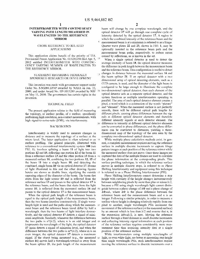
Interferometry is widely used to measure changes indistance and to measure the topology of a surface at themicro level. The latter application is often referred to assurface profiling. The general principle, illustrated withreference to a conventional interferometry system 100 (seeFIG. 1), involves splitting a beam 11 of light into twoportions 12 and 15, reflecting one portion 12 of the beam 11from a reference surface 13 and the other portion 15 from ameasured surface 16, combining the two portions 12, 15 ofthe beam 11 into a single beam 18, and detecting thecombined, single beam 18 via an optical detector 17. Beamsof light illustrated in this and the other drawing figuresherein are shown as double lines, signifying the outsideopposing edges of the diameter of the beam. The beam thatstarts from the light source 10 and is reflected from thereference surface 13 and passes to the optical detector 17 isthe reference beam, and the beam that starts from the lightsource 10, is reflected from the measured surface 16 andpasses to the optical detector 17 is the measurement beam.When the optical path length of the reference beam is
equal to the optical path length of the measurement beam,then the two beams interfere constructively. If single wave-length light is used and the paths along which the measure-ment beam and the reference beam travel differ by half awavelength, then the two beams of light interfere destruc-tively, and the optical detector 17 detects a signal of mini-mum amplitude. Similarly, whenever the difference betweenthe two paths is n*(a/2), where n is an odd integer and,represents the wavelength of the light, the optical detector17 again detects a signal of minimum level, and when thedifference between the two paths is m*(a/2), where m is aneven integer, the optical detector 17 detects a maximumsignal. If the object being measured (e.g., the measuredsurface 16) moves half a wavelength toward or away fromthe beam splitter 21, the path length of the measurement
2beam will change by one complete wavelength, and theoptical detector 17 will go through one complete cycle ofintensity detected by the optical detector 17. A region inwhich the combined intensity of the reference beam and the
5 measurement beam is at a minimum is referred to as a fringe.Quarter wave plates 22 and 23, shown in FIG. 1, may beoptionally inserted in the reference beam path and themeasurement beam paths, respectively, to reduce errorscaused by reflections, as is known in the art.
to When a single optical detector is used to detect the
average intensity of beam 18, the optical detector measuresthe difference in path length between the measurement beamand the reference beam. This configuration is useful to detect
15 changes in distance between the measured surface 16 andthe beam splitter 21. If an optical detector with a twodimensional array of optical detecting elements, such as aCCD camera, is used, and the diameter of the light beam isconfigured to be large enough to illuminate the complete
20 two-dimensional optical detector, then each element of theoptical detector acts as a separate optical detector, and thesystem functions as multiple interferometers operating inparallel. The area of each optical detector element creates apixel, a word which is a contraction of the words "picture"
25 and "element'. When the measured surface is not perfectlysmooth, there will be different optical path lengths fordifferent pixels, causing phase differences between the sig-nals at different optical detector elements and thereforedifferent intensity signals at each detector element. The
3o difference in intensity at different optical detector elementscan be converted to phase differences, and the phase differ-ences can be converted to distances, yielding a three-dimensional map of the topology of the area seen by thecomplete two-dimensional optical detector.
35 While multiple phase calculation methods exist, in gen-eral, a complete measurement requires moving the referencesurface in multiple discrete increments to capture fringepattern images at each position of the reference mirror whilethe measured surface does not move. Once these images are
40 captured the data of the multiple frames are used to calculatethe phase information at the corresponding pixels. Thissurface profiling technique, in which the reference surfacemoves in multiple discrete steps, is referred to as PhaseShifting Interferometry and equipment using this technique
45 is referred to as a Phase Shifting Interferometer (PSI).Phase Shifting Interferometers cannot determine a step
height with certainty if the height changes instantaneouslybetween neighboring pixels by more than plus or minus X/2,because a PSI using single wavelength light cannot distin-
50 guish between a phase change of A(D and a phase change ofA(D+na., where A(D is the phase difference between thereference beam and the measurement beam and n is aninteger. Following a similar principle, in order to measure asurface whose height is changing relatively rapidly from one
55 pixel to another, single wavelength PSIS increment themovement of the reference surface (or the measured surface)by an amount which is less than a/2 and assume that n, inthe expression A(D+n~/2, is zero. Moving the referencesurface through a fixed distance in small discrete increments
6o and collecting intensity signal information at each positionof the reference surface requires considerably more mea-surement time than acquiring intensity data at a singleposition of the reference surface.
While interferometers using multiple wavelengths of65 light, or even white light, are better at measuring step height
than single wavelength PSIS, such interferometers requiremoving the reference surface in discrete increments over a
US 9,464,882 B23
distance far greater than a/2, where X is the wavelength usedfor a single wavelength interferometer, requiring additionalmeasurement time.The lateral resolution of such a surface profiler is a
function of both the size of the elements in the opticaldetector and of the optics which image the measured surfaceonto the optical detector elements. In order to obtain betterlateral resolution, one uses greater magnification, resultingin a measurement of a smaller area of the measured surface.The software of typical Phase Shifting Interferometer sys-tems can stitch together multiple images, taken by measur-ing one site, moving the measured surface to another site,measuring at that site, etc., but taking multiple imagesrequires even more time. Further, the assumption behindstitching is that there is no system drift between adjacentimages, producing no discontinuities. Thermal drift andvibration can create errors in the stitched images. Errorscaused by stitching and the large amount of time required tomake measurements of suitable lateral and vertical resolu-tion often make PSIS unsuitable for quality control in aproduction environment.
Phase Shifting Interferometer measurements often sufferfrom error sources such as inaccurate knowledge of theexact position of the reference mirror and inaccurate posi-tioning of the intended discrete positions of the referencemirror. Further PSI interferometers cannot distinguishbetween vibration of the measured surface, such as might becaused by sound waves impinging on the measured surface,from changes in the actual roughness of the measuredsurface.
It would therefore be desirable to have interferometrysystems and methods that avoid at least some of the draw-backs of the conventional interferometry systems and meth-ods described above.
SUMMARY
In accordance with the present application, interferometrysystems and methods are disclosed in which the path lengthof a reference light beam, measured in wavelengths, iscontinuously changing in sinusoidal fashion, and the inter-ference signal created by combining a measurement lightbeam and the reference light beam is processed in real timeto obtain the physical distance along the measurement lightbeam between a measured surface and a spatial referenceframe such as a beam splitter. The processing involvesanalyzing the Fourier series of the intensity signals at one ormore optical detectors in real time, using the time-domainmulti-frequency harmonic signals to extract the phase infor-mation independently at each pixel position of one or moreoptical detectors, and converting the phase information todistance information.
In accordance with a first aspect, the path length of thereference beam changes in a sinusoidal oscillatory fashion.A beam splitter splits a light beam generated by a lightsource into a first portion and a second portion. Further, areference surface is disposed substantially perpendicular tothe first portion of the beam, and a measured surface isdisposed substantially perpendicular to the second portion ofthe beam. The reference surface moves toward the beamsplitter and then away from the beam splitter, while main-taining substantial perpendicularity to the first portion of thebeam, in a continuous oscillatory manner that is sinusoidal.The frequency of oscillation of the reference surface isgenerally lower than the rate at which the optical detectorcollects data, allowing multiple sets of data per period ofoscillation of the reference surface.
4The waveform of the intensity at the optical detector is
I=A+B cos (A(p* sin (w,t)+(p),
where A is a DC signal offset, w,, is the angular frequency of5 the motion of the reference surface, B is the intensity
amplitude of the waveform, ~ is the fringe phase (heightinformation), and A~ represents the amplitude of the refer-ence mirror modulation or oscillation.The phase difference information is recovered by real-
io time analysis of this waveform, enabling a surface profilemeasuring system in which the test object does not need tobe stationary during the measurement. For example, themeasured surface can move in the X direction, via themotion of a stage holding the sample or any other suitable
15 mechanism and using one or more position encoders or anyother suitable mechanism to determine the precise positionof the moving sample, while the system measures in the Ydirection. In accordance with this first aspect, the system candetect the phase synchronously, providing surface profile
20 data with high signal-to-noise-ratio (SNR) since noise offrequencies that are not multiples of w,, will be filtered out.
In accordance with a second aspect, the optical detector isa two-dimensional array of optical detector elements and theoutput from the optical detector is two-dimensional intensity
25 data. In accordance with an exemplary aspect, if it isnecessary to measure a surface which is larger than the areaof the second portion of the beam, then after acquiring oneimage, the measured surface is displaced in X or Y, thesystem waits to allow vibration caused by the motion to
so settle, a new image is acquired, and the system softwarestitches together the images. The same concept can beextended to acquire additional images, after additionalmovement of the measured surface in either the X or Y axis,or a combination of both.
35 In accordance with a third aspect, the optical detector isat least a linear array of optical detector elements andproduces one dimensional intensity data, for instance in theY direction. In accordance with an exemplary aspect, themeasured sample moves in the X direction while intensity
4o data in the Y direction are acquired. The effective imagecreated by moving the measured sample can be much largerthan that available by using an optical detector that suppliesintensity data in two dimensions. If it is necessary tomeasure larger surfaces, then it is possible to move the
45 measured surface in the Y direction, wait for settling, andthen acquire new data while moving the measured surface inthe X direction. Similarly, the measured sample could movein the Y direction, and the linear array of optical detectorelements could be mounted to take data in the X direction.
50 In accordance with a fourth aspect, which is useful whenmeasuring round flat objects, such as the surface of magnetichard disks, the one dimensional array of optical detectorelements and/or the measured surface can be configured tomove relative to one another to allow the one dimensional
55 optical detector to perform a measurement along a radius ofthe measured surface. In accordance with an exemplaryaspect, the one dimensional array of optical detector ele-ments measures along such a radius and the measuredsurface is rotated about its center as pixel data are collected.
60 If the length of the one dimensional optical detector is lessthan the radius needed to be measured, then multiple imagescan be acquired by moving the linear array of opticaldetector elements in the appropriate direction along theradius and acquiring data during another rotation of the
65 measured surface. To minimize measurement time, whilemaintaining a constant effective pixel size, the speed ofrotation of the measured surface may be increased as the

US 9,464,882 B2
5distance of the linear array of optical detector elements fromthe center of rotation decreases.
In accordance with the third and fourth aspects describedabove, the sample moves in one direction, while a lineararray of optical detector elements positioned in a substan- 5
tially perpendicular direction collects intensity data. Theimage captured during one complete movement of thesample can be increased by increasing the length of thelinear array of optical detector elements. This can beachieved by various mechanisms or techniques, including to
increasing the physical length of the array of optical detectorelements or by using multiple interferometers, includingmultiple linear arrays of optical detectors, operating inparallel and positioned to extend the equivalent length of a 15single array.The interferometry system according to the first aspect
described above is useful for distance measurement, wherethe measured surface moves. The method of phase detectionvia analyzing the complex waveform produced by the oscil- 20lating reference mirror and the moving measured surface canbe implemented at lower cost than conventional methods,and the performance requirement of the analog to digitalconverter used to digitize the intensity signal can be lowerthan required by conventional methods. 25
In accordance with the second, third, and fourth aspectsdescribed above, it is desirable to process intensity data fromall the optical detector elements in parallel, in order to createreal time, time-domain data. This can be achieved viapipe-lining, in which the same hardware quickly processes 30
data from one optical detector element and then processesdata from the next optical detector element at the followingprocessor clock cycle, producing fully processed data at arate that can be as fast as the rate that data are captured by 35the entire group of optical detector elements. If lower spatialfrequency of the image is allowable, then the rate of datacapture can be even faster.
In accordance with a fifth aspect, a data processingapproach, referred to herein as "active mixing", allows 40producing fully processed optical detector intensity data at arate equal to the rate that intensity data are captured by theoptical detector. In accordance with a sixth aspect, anotherdata processing approach, which is referred to herein as"pseudo-active mixing", allows producing fully processed 45data at one quarter the rate at which data are captured by theoptical detector, without the need for modulating the lightintensity, thus without incorporating an electro-optic com-ponent that can increase cost.
In accordance with a sixth aspect, an interferometry 50system includes a beam splitter operative to split a sourcelight beam into a reference beam and a first measurementbeam. The reference beam and the first measurement beameach have an associated path, and an associated path lengthmeasured in wavelengths. A measured sample is disposed in 55the path of the first measurement beam. The interferometrysystem further includes a first component operative to varythe path length of the reference beam in a sinusoidal fashion.In addition, the interferometry system includes at least onesecond component operative to detect at least one second 60measurement beam that is based upon the reference beamand the first measurement beam, to generate at least oneoptical detector signal corresponding to the second measure-ment beam, and to analyze Fourier series components of theoptical detector signal in the time-domain to determine a 65phase shift in the reference beam or the first measurementbeam caused by the measured sample, a change in the path
6length of the reference beam or the first measurement beam,and/or a distance between the beam splitter and the mea-sured sample.The presently disclosed interferometry systems and meth-
ods can acquire surface topology data of a large measuredsurface at a rate which is faster than conventional systemsand methods. Further, the disclosed systems and methodscan provide fast surface profile measurements withimproved vertical resolution and measurement accuracy.Moreover, the disclosed systems and methods have theability to capture a high resolution single measurementimage of an area that is larger than previously possible usingconventional systems and methods. The disclosed systemsand methods can also acquire data in real time in order toallow time-domain digital filtering techniques. In addition,the disclosed systems and methods allow simultaneousmeasurement of a known measured surface, and anunknown measured surface, in order to correct for system-atic measurement errors.
Other features, functions, and aspects of the invention willbe evident from the Drawings and/or the Detailed Descrip-tion of the Invention that follow.
BRIEF DESCRIPTION OF THE DRAWINGS
The invention will be more fully understood with refer-ence to the following Detailed Description of the Inventionin conjunction with the drawings of which:FIG. 1 is a schematic diagram showing a conventional
Michelson interferometer;FIG. 2 is a schematic diagram showing an interferometry
system configured for surface profiling, in accordance withan exemplary embodiment of the present application;FIG. 3 is a schematic diagram showing an interferometry
system with quarter wave plates and a moveable referencesurface, in accordance with another exemplary embodimentof the present application;FIGS. 4a and 4b are diagrams showing the motions of a
measured part with reference to a linear array of opticaldetector elements, in accordance with further exemplaryembodiments of the present application;FIG. 5 is a diagram showing the measurement of a surface
with high spatial frequency in one axis;FIG. 6 is a block diagram showing a data path;FIG. 7 is a schematic diagram showing a method of
correcting systematic errors in collected data, in accordancewith still another exemplary embodiment of the presentapplication;FIGS. 8a and 8b are block diagrams illustrating over-
views of the data processing done by a signal processingcomponent;FIG. 9 is a schematic diagram showing an illustrative
example of pipe-lining;FIG. 10 is a series of plots showing the signals in an active
mixing signal processing technique;FIG. 11 is a series of plots showing the signals in a
pseudo-active mixing signal processing technique; andFIG. 12 is a block diagram illustrating an overview of
further data processing done by a signal processing compo-nent.
DETAILED DESCRIPTION
The disclosure of U.S. Provisional Patent Application No.61/620,658 filed Apr. 5, 2012 entitled INTERFEROMETERWITH CONTINUOUSLY VARYING NUMBER OF

US 9,464,882 B2
7WAVELENGTHS TO THE REFERENCE MIRROR isincorporated herein by reference in its entirety.
FIG. 2 shows an interferometry system 200, such as aMichelson interferometer, functioning as the optical sensingapparatus for surface profiling. It includes of a monochro-matic light source 212, a beam expander 214, a beam splitter218 with partially mirrored surface 216, a reference mirror202 with reference surface 204, a measured surface 210, anobjective lens 220, and an optical detector 222.The monochromatic light source 212 emits a light beam
226. The diameter of the beam 226 is enlarged via the beamexpander 214 to produce a light beam 228 whose diameteris large enough to illuminate the desired image area of themeasured surface 210. For example, the diameter of thebeam 226 might be 2-3 mm, and the beam expander 214might be a I0x beam expander, to produce the beam 228whose diameter is 20-30 mm. The beam 228 is split into twoportions of approximately equal intensity 224a and 230a, forexample via the beam splitter 218 whose internal mirroredsurface 216 is approximately 50% reflective to the wave-length of light emitted from the light source 212 at an angleof incidence of 45 degrees. Such beam splitters are com-monly available. For example, the model CMI-BSI beamsplitter, manufactured by Thorlabs, or any other suitablebeam splitter, may be employed. It is noted that a parallelplate mirror can be used instead of a beam splitter cube.The beam 224a reflects from the reference surface 204
and creates a light beam 224b. Similarly the beam 230areflects from the measured surface 210 and creates a lightbeam 230b. The reflected beam 224b enters the beam splitter218, and approximately 50% of the beam travels through thepartially mirrored surface 216 toward the optical detector222. Similarly the reflected beam 230b travels toward thebeam splitter 218 and is reflected from the partially mirroredsurface 216 toward the optical detector 222. Thus, the lightbeam 232 is a combination of the beam 224b reflected fromthe reference surface 204 and the beam 230b reflected fromthe measured surface 210.The reference surface 204 is the surface of the reference
mirror 202. The reference mirror 202 is positioned with thereference surface 204 substantially perpendicular to thebeams 224a, 224b. The reference surface 204 is substan-tially flat, and portions of the beam 224b reflected from onearea within the reference surface 204 experience substan-tially the same optical path length as portions of the beam224b reflected from other areas within the reference surface204. Reference mirrors with flat surfaces are commonlyavailable in different flatness specifications. Deviations froman ideal, perfectly flat, reference mirror create systematicerrors in the measurement. These errors can be subtractedfrom the measurement of the measured surface, by storingthe error at each optical detector element, determined whenmeasuring a known, flat surface.The beam 232 passes through the objective lens 220 and
onto the optical detector 222. The optical detector 222 canbe a single point detector, a linear array of optical detectorelements, a two-dimensional array of optical detector ele-ments, or any other suitable optical detector. In the case ofeither a linear array of optical detector elements, oftenreferred to as a "linear detector", or a two-dimensional arrayof optical detector elements, each element creates one pixelof information. The physical size of each element, reducedby the magnification of the objective lens determines themeasurement area of each pixel. For example, an opticaldetector element whose physical size is a square area 10microns on a side and a 5x objective lens allows measuring2 micron pixels of the measured surface.
8FIG. 3 shows an interferometry system 300, in which the
optical path length of the beams 224a, 224b can change inan oscillatory fashion when the reference surface 204 movestoward the beam splitter 218 and away from the beam
5 splitter 218, while maintaining substantial perpendicularityto the beams 224a, 224b. A motion of the reference surface204 of length x in the direction towards the beam splitter 218causes the optical path length to decrease by 2x. Similarly,a motion of the reference surface 204 of x away from the
io beam splitter 218 causes the optical path length to increaseby 2x. FIG. 3 illustrates an exemplary method of achievingthis motion. In FIG. 3 the reference mirror 202 is attachedto a substantially fixed, high mass object 342 via threepiezoelectric transducers (PZTs) 340a, 340b, and 340c.
15 PZTs 340a, 340b, and 340c are controlled by three highvoltage amplifiers (not shown), and when the voltage acrosseach PZT increases, the PZT changes length, moving thereference mirror 202 in a direction toward or away from thebeam splitter 218, while maintaining perpendicularity to the
20 beams 224a, 224b. When the voltage across a PZT returnsto its original value, the length of the PZT returns to itsoriginal value. High voltage of the opposite polarity createsa change in the PZT length in the opposite direction. Thethree PZTs 340a, 340b, and 340c and their associated high
25 voltage amplifiers are matched so as to maintain substantialperpendicularity to the beams 224a, 224b as the PZTs 340a,340b, and 340c move the reference surface 204 toward thebeam splitter 218 and away from it. The object 342 has veryhigh inertial mass compared to the reference mirror 202, and
3o as the PZTs 340a, 340b, and 340c move the reference mirror202, substantially all of the motion is movement of thereference mirror 202 containing the reference surface 204,with substantially no motion of the fixed object 342. Thethickness of the reference mirror 202, the material of the
35 reference mirror 202, and the placement of the PZTs 340a,340b, and 340c are chosen to avoid dynamic changes inflatness of the reference surface 204 as it moves toward thebeam splitter 218 and away from it in response to excitationfrom the PZTs 340a, 340b, and 340c. Putting a beam
40 expander (not shown) in the path of the beams 224a, 224bcauses the beam diameter hitting the reference surface 204to be smaller than the beam diameter of the beams 224a,224b, allowing the reference mirror 202 to be smaller andhave lower mass. Thus it is possible to move the reference
45 mirror 202 back and forth more rapidly without requiringmore powerful PZTs and without incurring significantdynamic distortion of the reference surface 204.
It is noted that any other suitable mechanisms of mount-ing the reference surface 204 and moving it in an oscillatory
50 motion may be employed, such as using a single PZT and aflexure mount. As an example, the movement of the refer-ence mirror 202 via a PZT can be accomplished by themodel P-720 PZT, manufactured by Physik Instrumente,GmbH. Moreover, while the examples shown in FIGS. 3, 4
55 and 6 use a Michelson interferometer configuration, anyother suitable interferometer configuration, including Mirau,Fizeau, Fabry-Perot, Twyman-Green, and Mach Zehnder,could also be used.An alternative to moving the reference mirror 202 with
60 the reference surface 204 is modulating the wavelength ofthe light source 212. In any of the illustrative embodimentsdisclosed herein, the oscillation of the wavelength of lightcan be substituted for the oscillatory motion of the referencemirror. Many techniques exist to modulate the wavelength
65 of a coherent light source. One economical technique is tomodulate the current of a laser diode, such as SanyoDL6147, to produce wavelength modulation. If the path

US 9,464,882 B29
length of the reference beam differs by AL from the pathlength of the measurement beam, then a wavelength shift ofAX of the light source 212 causes a phase shift of theinterference fringe of 27cALAX/X2. Signal processing cancorrect for the consequential effect of changes in lightamplitude caused by modulating the laser diode current inorder to modulate the wavelength.An interferometry system in which the wavelength of the
light beam 228 is modulated instead of moving the referencemirror 202 is described below with regard to FIG. 3. In suchan interferometry system, because the reference mirror 202is not moved, the PZTs 340a, 340b, and 340c, as well as thehigh mass object 342, may be omitted. Further, one ofordinary skill in the art will appreciate that the wavelengthof the light beam 228 can be modulated by placing an opticalcomponent such as an acousto-optic modulator in the path ofthe light beam 226 emitted by the light source 212 or in thepath of the light beam 228 produced by the beam expander214, or by any other suitable technique.
Modulating the wavelength of the light beam 228 insinusoidal fashion typically allows a higher modulationfrequency than moving the reference mirror 202 and pro-duces a system with no moving parts. Further, modulatingthe wavelength of the light beam 228 obviates the need forthe high mass, substantially fixed object 342, reducing themass of the total system. When using a laser diode as a lightsource, the change in intensity caused by modulating thediode current can be predicted or measured by a photodetector located near the laser diode, and the signal process-ing apparatus can correct for the change in light intensity ofthe laser diode.
In a first illustrative embodiment of the present applica-tion, a single point optical detector is used, the referencemirror moves continuously in sinusoidal motion, and thesignal processing apparatus determines phase informationby analyzing the output of the optical detector. Such aninterferometer is useful for measuring changes in distance.
In a second illustrative embodiment of the present appli-cation, a two-dimensional optical detector is used, the ref-erence mirror moves continuously back and forth in sinu-soidal motion, or the wavelength of the light source changesin sinusoidal fashion, and the signal processing apparatusdetermines phase information by analyzing the output ofeach element of the optical detector. Phase information isconverted to distance information by knowing the wave-length of light produced by light source 212. The imagecaptured by the two-dimensional optical detector is equal tothe physical size of the two-dimensional optical detector,reduced by the magnification of objective lens 220. Tomeasure surfaces larger than one image size, it is necessaryto move the measured surface in the X or Y direction, asappropriate, to a previously unmeasured area, wait for thestage motion and any associated vibration to settle, andcapture an additional image. The process of moving to a newposition, waiting for motion transients to settle, and thenrepeating the previous acquisition process is referred to as a"Step and Repeat" process. Additional images can be cap-tured until the complete surface has been measured, up to thelimit of the mechanical stage that moves the measuredobject. The edge of each additional image should eithertouch the previous image or overlap the previous image veryslightly. The data from the additional image can be stitchedto the original image via software.
In a third illustrative embodiment of the present applica-tion, the optical detector is a linear array of detector ele-ments positioned for instance in the Y direction. The refer-ence mirror moves continuously back and forth toward and
10away from the beam splitter in sinusoidal motion, or thewavelength of the light source changes in sinusoidal fashion,and the signal processing apparatus determines phase infor-mation by analyzing the output of each element of the
5 optical detector. The sample moves in the X direction whileimage data are being acquired, as shown in FIG. 4a. Thepixel size in the Y direction is equal to the physical size ofa detector element divided by the magnification of objectivelens 220. The pixel size in the X direction in this example is
10 equal to the speed of sample movement in the X directiondivided by the detection rate. The detection rate is dependenton both the frame rate of the optical detector and the signalprocessing technique used to detect phase changes. Themaximum detection rate achievable is the frame rate, with
15 some signal processing techniques achieving slower ratessuch as fps/2, fps/4, and fps/64, as are disclosed herein,where fps is an abbreviation for frames per second.For example a sample moving at 1400 millimeters per
second in the X direction and an optical detector sampling20 at 140,000 frames per second can produce a pixel size in theX direction of 10 microns, when using a signal processingtechnique that can detect phase information using only oneframe of image data. The Y dimension of the image sizecreated using this illustrative embodiment is equal to the
25 physical length of the linear optical detector reduced by themagnification of objective lens 220. The X dimension of theimage size created using this illustrative embodiment isequal to the X distance moved by the sample divided by thedetection rate. To measure a surface of larger area, it is
30 possible to perform a Step and Repeat operation, as previ-ously described, and stitch together multiple images.In this example, the measured surface is divided into
many 10 micron by 10 micron pixels, so according to theNyquist sampling theory it is possible to detect changes in
35 surface topology having a spatial frequency of 1/(2*10microns), or 50 cycles per millimeter. The amplitude of thetopology variations that can be detected is dependent on themodulation frequency of the optical path length and thestage scan speed. In the case of using a HeNe laser source
40 of wavelength 632 nm, modulating the reference mirror by316 nm peak to peak, and using a camera sampling at140,000 frames per second, the system can detect a maxi-mum height difference of 316 nm from one pixel to the nextin the Y-direction or between frames of the pixel in the
45 X-direction.The minimum required modulation frequency w,, of the
reference beam path length or the light source wavelengthdepends on the choice of demodulation technique, and thepresent application discloses four techniques, as follows,
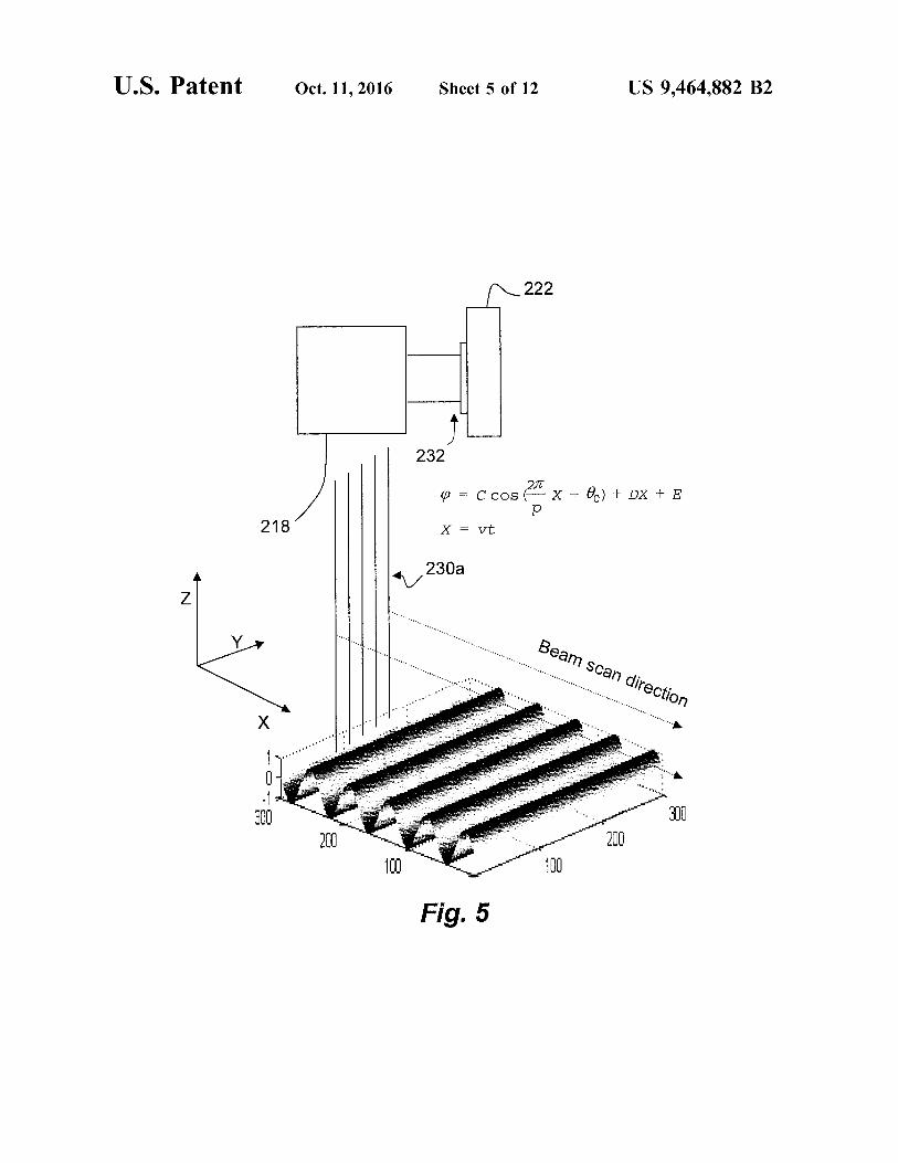
50 1. Active mixing2. Pseudo-active mixing3. Multi-frequency analysis, and4. Multi-frequency analysis via Phase Locked Loop.When using active mixing, pseudo-active mixing, or
55 multi-frequency analysis (without phase locked loop) theminimum required modulation frequency w,, is a function ofthe camera frame rate, the required surface profile spatialresolution, the speed of movement of the measured sample,and the profile accuracy. If the surface structure has a period
60 of p in the X direction as shown in FIG. 5, the fringe phasethat the jth pixel would see can be expressed as
/
p
2n65 111
~i = CCosl — X + Bo) + DX + goo.

US 9,464,882 B211
D is the deviation from absolute perpendicularity betweenthe measurement beam and the average measured surface, 00is the offset of the phase, and ~0 is the offset of the w,,modulation. In practice, when the measurement sample isaligned such that it is substantially perpendicular to themeasurement beam, then D can be considered zero. Whenthe beam position moves at a constant speed v, a plot of thephase output versus time is a cosine function. The faster themeasured surface moves under the measurement beam thehigher frequency of the output intensity signal. The modu-lation frequency can thus be expressed as
dip, 27ry /2tryw,»
dt =—C p sinl p t+00)+Dv.
When signal processing incorporating a phase lockedloop, such as the known method disclosed in U.S. Pat. No.7,430,484, or any other suitable method is used, the mini-mum modulation frequency of w,, can be 3-4 times lower forthe same stage movement speed.
In a fourth illustrative embodiment of the present appli-cation, the optical detector is a linear array of opticaldetector elements positioned to look at the radial direction ofa circular measured surface, as shown in FIG. 4b. Forexample, the linear array of optical detector elements and/orthe circular measured surface can be configured to moverelative to one another to allow the optical detector toperform a measurement along a radius of the measuredsurface. In accordance with the illustrative embodiment ofFIG. 4b, the reference mirror moves continuously back andforth in sinusoidal motion, or the wavelength of the lightsource 212 is modulated in sinusoidal fashion, and the signalprocessing apparatus determines phase information by ana-lyzing the output of each element of the optical detector. Themeasured object rotates about an axis 32 which passesthrough the center point of the measured object with themeasured surface 36 substantially perpendicular to the mea-surement beam 230a. Image data are being acquired whilethe surface 36 is rotating. The pixel size in the radialdirection is equal to the physical size of an optical detectorelement divided by the magnification of the objective lens220. The pixel size in the theta direction is equal to theangular rotational speed of sample movement, times theradius of the pixel being measured, divided by the detectionrate. While the size of a pixel in the theta direction is notconstant due to the differing radii of each optical detectorelement, this difference can be readjusted later when pre-senting data. It is possible to acquire multiple images, inStep and Repeat fashion, by moving the linear array ofoptical detectors in the radial direction after acquiring animage of one complete revolution of the sample. The speedof rotation of the sample can be changed when acquiringdifferent images in order to reduce the angular variation inpixel size and reduce the total measurement time.
Referring to FIG. 6, the signals from each pixel in theoptical detector 222 are captured, digitized by a digitizer 29,transferred to a frame grabber 30, and fed to a signalprocessing component 31, such as a GPU, a Field Program-mable Gate Array (FPGA), or any other suitable signalprocessing component. Xilinx Spartan 3A DSP 1800A is anexample of a suitable FPGA.Some optical detectors include the capability to digitize
the optical intensity of each pixel, and other optical detectorsproduce an analog output which must be digitized externalto the optical detector.
12All of the illustrative embodiments of the present appli-
cation described above can measure distance in units of theaverage wavelength of light emitted from the light source212. Unforeseen short-term changes in wavelength therefore
5 create measurement errors. These errors, and similar errorssuch as might be caused by a change in the refractive indexof air, can be avoided, as shown in FIG. 7.FIG. 7 shows an interferometry system 700, in which an
additional optical detector element 706a can be positionedio adjacent to optical detector elements 706b, 706c within the
optical detector 222 previously described. Further, an addi-tional fixed measured surface 702 can be positioned adjacentto the measured surface 210, such that the physical pathlength of the additional measured surface 702 does not
15 change when the physical path length to the measuredsurface 210 changes. Changes in the phase of the intensitysignal from each pixel of the measured surface, once con-verted to distance, can be multiplied by the ratio of theoriginal phase of the pixel measuring the fixed surface to the
20 current phase of the pixel measuring the fixed surface tocompensate for change in wavelength or refractive index.This correction can be made in real time, because all pixeldata are sampled at the same time, and the data are processedin parallel by the signal processor 31.
25 The optical configuration is shown in FIG. 7. The surface702 is the fixed surface, and the surface 210 is the measuredsurface. The beam 230a is large enough to strike both themeasured surface 210 and the fixed surface 702. The beam230b is reflected by the partially mirrored surface 216 and
30 then combined with the portion of reflected beam 224b thatis transmitted through the partially mirrored surface 216.The combination of those beams, namely, the beam 232,enters the lens 220 and is expanded to become beams 704a,704b, 704c. Specifically, the beam 704c is the ray of light at
35 one side of a complete beam comprising beams 704a, 704b,704c, the beam 704b is the ray at the center of the completebeam, and the beam 704a is the ray at the side of thecomplete beam opposite the beam 704c. The optical detector222 in this example is a linear array of optical detector
40 elements 706a, 706b, 706c. The beam 704c is detected bythe optical detector element 706c, the beam 704b is detectedby the optical detector element 706b, and the beam 704a isdetected by the optical detector element 706a.The waveform of the intensity for each pixel can be
45 expressed as
I(x y,t)=A(x y)+B(x,y)cos(A~*sin(w,t)+(P(x,y,t))
where x and y represent the location of the position beingmeasured, A is a DC signal offset which may vary from one
50 measurement site to another, w,, is the angular frequency ofthe modulation of the reference surface position or thewavelength, B is the intensity amplitude of the waveform, ~is the phase of the fringe pattern as a result of interference,and A~ is the range of phase shift due to motion of the
55 reference mirror. The DC offset term can be ignored, and theremainder of the equation can be represented by a Fourierseries as follows.
60 I(x, y, t) = B(x, y)cos(A~o * sin(m,t) + ~o(x, y, t)) = (1)
BJO(A~o)cos(~o) — 2Bsin(~o)E[J2._1(A~o)sin((2m —1) * w.t)]
+2Bcos (~o)E [J2. (A~o)cos (2ma),t)] (2)
65 where the summation is from m 1 to -, 7,(A~) for i-0, 1,2.... are Bessel functions, and the DC signal offset term isomitted for simplicity. An exemplary method of measuring
US 9,464,882 B213
the phase ~ of each pixel location is to calculate the arctangent [a*SN(~)/CS(~)] at that location, where a is aconstant dependent only on A~. The term SN(~) is used asa short-hand for the demodulated result using odd harmonicsin the output signals, I(x,y,t), such as —B sin(~,x,y,t){71(A~)+73(A~)+75(A~)+ ... 1. The constant gain —B{71(A~)+73(A~)+75(A~)+ ... } for sin(~,x,y,t) could vary depending on thesynthesized oscillator configuration. The term CS(~) is usedas a short-hand for the demodulated result using evenharmonics signals, such as B cos*x1y1t){72(A~)+74(A~)+76(A~)+ ... 1. Again, the constant gain for cos(~,x,y,t) couldvary depending on the synthesized oscillator configuration.Therefore once these terms SN(~) and CS(~) are obtainedfor each pixel X,Y position, the distance Z at each pixel canbe calculated. With this exemplary method, the noise spec-trum outside of the fringe oscillation frequency and itsharmonics is effectively eliminated by a phase synchronousdetection technique, while the measurement range can bewell beyond the fringe period.
Similar waveforms produced by position encoders areknown. Further, methods of calculating position informationfrom such output signals are also known, e.g., by using aprobe or a sensor that moves in a sinusoidal motion parallelto a grating surface and substantially perpendicular to thedirection of the grating stripes, as disclosed in U.S. Pat. Nos.5,589,686, 5,744,799, 6,639,686, and 7,430,484, which areincorporated herein by reference in their entirety.The signal processing shown in FIG. 8a determines phaseof the intensity signal by calculating sinO and cosO and
taking the arc tangent. Multiplying the intensity signalI(x,y,t) by cos(2w t) and filtering through a low pass filtercreates the coefficient for m 1, 'h*B cosW72(A~). Simi-larly, multiplying the intensity signal I(x,y,t) by sin(wt) andfiltering through a low pass filter creates the coefficient form=1, 1/2*13 sin(~)71 (A~).
(P=arc tangent(Ji(A~)/Jz(4(P)*[ifz*B cos((P)Jz(4(P)]/
[iiz*B sin((P)Ji(4(P)]).
SinO in the Fourier series of equation 2 has a coefficientof 2B*E[72m_1(A~)sin((2m-1) *wt)], and cos( ) has a coef-ficient of 2B*E[72m(A~)cos(2mw t)]. The constant shown inFIG. 8a is the ratio of the cosO coefficient divided by thesinO coeff cient. The arc tangent function can be computedvia a look-up table, a numerical processing algorithm, or anyother suitable technique.The output of the arc tangent computation is ~, which can
be converted to a distance by multiplying by
A47r
The actual measured distance is ~+na., where n is an integer.The process of determining the value of n is referred to as"phase unwrapping". Phase unwrapping is done by compar-ing the distance measured at one pixel to neighboring pixelsand picking a value of n such that the difference between apixel and its neighbor is less than k/2.
Multiplying the I(x,y,t) signal by cos(4w t) and sin(3w t)creates the coefficients of sinO and cos( for the case ofm=2, and adding the coefficient for m=1 to the coefficient form=2 before computing the arc tangent creates an improveddetermination of ~. Computing the coefficients of sin( ) andcos( using additional values of in creates a better deter-mination of ~. FIG. 8b shows how the signal processingwould determine ~ using m=1 through m=4, inclusive.
14Alternatively, a pseudo-phase-locked loop (PLL) can be
used to create an estimate of the phase ~, ~, and to computecos(~)sin(nw,,t), where n is an odd integer, and sin(~)cos(mw,,t), where in is an even integer, and multiply-add the
5 incoming intensity signal I(x,y,t) by the synthesized func-tions with the estimated quadrature components, forexample, as described in U.S. Pat. No. 7,430,484. The PLLconstantly adjusts the estimate of phase ~ so that sin( —~) iszero, and determines the reference mirror oscillation ampli-
10 tude A~) rather than requiring A~ as an input, therebyeliminating errors caused by variation in or an inaccuratevalue of A~, the reference mirror oscillation amplitude.In the second, third, and fourth illustrative embodiments
15 of the present application described above, the data for alloptical detector elements are processed in substantially realtime, in parallel. This may be done either via multipleprocessor cores or preferably by an FPGA (Field Program-mable Gate Array), a GPU (Graphics Processing Unit), or an
20 ASIC (Application Specific Integrated Circuit) utilizingpipe-lined signal processing, in which the same hardwarequickly processes an intensity datum from one opticaldetector element and then processes an intensity datum fromthe next optical detector element by transferring the output
25 from each node to the next processing node at each clockcycle of the processor, producing fully processed intensitydata at a rate that can be as fast as the rate that data arecaptured by the optical detector with a delay of only a fewclock cycles of the pipe-line.
30 FIG. 9 shows an exemplary signal processing flow usingpipe-lining, although variations are possible. Intensity infor-mation h coming out of the camera, where j refers to the rowj of the linear optical detector array in the third illustrative
35 embodiment is fed into the processor core through thememory array, MA3 at every clock cycle. Each sine andcosine signal is multiplied by an appropriate gain, which isdetermined from a look-up table. All the cosine terms and allthe sine terms are added. When the jth pixel data is multi-
40 plied by the synthesized multi-frequency signals, the resultis fed into a low pass filter at the next processor clock cyclein order to deriveA*SN(~) and B*CS(~), where and B areconstants. While this is happening, processing of the nextintensity signal starts at the previous functional node. The
45 low pass filters have a few intermediate states which corre-spond to a pixel position. Such states are stored in FIFO-likememory MAl, and are later restored immediately before thenext corresponding pixel operation is executed. The inter-mediate result from the lower signal path is then multiplied
5o by the constant depending on the gain matrix inside GainLUT. The last signal processing core first calculates arctangent(S/C). The arc tangent function creates an output ~,whereas what is needed is ~+n7t where n is an integer, suchthat the difference in phase between the current pixel and the
55 same pixel in the next frame is less than 71, in order toguaranty continuity. This process of phase unwrapping is thelast step in the signal process flow shown in FIG. 9. Eachphase measurement result is stored in memory array MA2and is later compared with the arc tangent output at the same
60 pixel position at the next frame. If the difference is more than71, the latest phase measurement result is readjusted by ±7idepending on the surface profile until the absolute phasedifference becomes less than 71.
Alternatively, the PLL signal processing method dis-65 closed in U.S. Pat. No. 7,430,484 can be used for pipe-lined
processing. Use of this technique creates automatic phaseunwrapping, as the input to the numerical integrator in the
US 9,464,882 B215
feedback loop constantly shows the phase being measuredand automatically maintains continuity as the measuredphase changes.
Pipe-lining makes it economically feasible to process alldata from the optical detector elements in real time, evenwhen there are millions of pixels in the image. Further, theprocessing techniques described in the above listed U.S.patents allow resolution of phase measurement equivalent toone part in 218. Thus the Z-axis resolution of the measure-ment when using a Michelson interferometer and light of632 nm wavelength is 1.2 pm.The signal processing method described thus far is
referred to as a "multi-frequency" analysis method. Thismethod requires a good digital representation of the inputsignal I(x,yt). Typically 64 or more samples per period ofpath length modulation frequency w,, are required, especiallywhen analyzing higher order harmonics. Providing 64samples via an optical detector array such as a CCD camerarequires 64 frames of data. In the second, third, and fourthillustrative embodiments described above, the measuredobject is moving during data acquisition and therefore theeffective pixel dimension in the direction of movementequals the distance traveled divided by the effective framerate, which has been referred to as the "detection rate".
Making the detection rate '/64 the camera frame rate limitsthe total measurement speed. This problem can be addressedby avoiding the initial multiplication of the digitized inten-sity waveform shown in FIGS. 8a and 8b. Employing a lightintensity modulator 1202 (see FIG. 12) to modulate thephysical light intensity of the light source 212 (see also FIG.12) by sin(w t), with the light modulation frequency, w,,,synchronous with the camera frame rate, produces a signalwith the same information as multiplying the intensity signalI(x,yt) produced using a light source of constant intensity bysin(w,t). Similarly, employing the light intensity modulator1202 to modulate the physical light intensity of the lightsource 212 by cos(2w t) produces a signal with the sameinformation as multiplying the intensity signal I(x,yt) pro-duced using a light source of constant intensity by cos(2w t).When multiplication is done digitally it is possible to
multiply the intensity signal I(x,yt) by sin(wt) and also bycos(2w,t) and produce two outputs at the same time. Whenmodulating the physical light intensity rather than the inten-sity signal I(x,yt), the physical light intensity can only bemodulated by a single waveform. Since it is necessary toobtain both sin( and cos( information one can modulatethe physical light intensity by sin(wt) for one cycle, modu-late the physical light intensity by cos(2w t) for the nextcycle, repeat the sequence, combine information obtainedfrom different cycles to obtain the sin( and cos(, andcompute the arc tangent [sin(~)/co s( )] (see FIG. 12, refer-ence numeral 1208). Since the sine and cosine functionsinclude both positive and negative values, the intensitysignal is actually modulated by [1+sin(w t)] and [1+cos(2w,t)], and the DC level is removed during signal process-ing. FIG. 10 shows one example of waveforms producedwhen modulating the physical light intensity in this manner.
Define +S as the photon signal arriving at the opticaldetector 222 (see FIG. 12) during one cycle of path lengthmodulation of frequency ~,, when the physical light intensityis modulated by sin(~,t). Define +C as the photon signalarriving at the optical detector 222 during one cycle of pathlength modulation of frequency ~,, when the physical lightintensity is modulated by cos(2~,,t), which in this example isduring the second modulation cycle. During the third cycle,—S is obtained when the physical light intensity is modulatedby —sin(~J). During the fourth cycle, —C is obtained when
16the physical light intensity is modulated by —cos(2~,,t). Thesequence then repeats, with the fifth cycle being the same asthe first, the sixth cycle being the same as the second, etc.
Define d as the DC offset of the pixel intensity signal5 caused by the fact that the physical light intensity was
modulated by [1+sin(~J)] rather than by [sin(~J)] and[1+cos(2~,t)] rather than [cos(2~,.t)]. The optical detector222 (such as a CCD camera) integrates the incoming pho-tons within a finite time window per frame. This integration
io performs a function equivalent to the low pass filter of FIG.8a or 8b. As a result, the integration operation of the opticaldetector 222 (see FIG. 12) denoted as <> below, provides theoutput signals of al, a2, a3, and a4 shown in FIG. 10 duringeach frame as follows (see also FIG. 12, reference numeral
15 1204).
a1=<+S+d> (3)
a2=<+C+d> (4)
20 a3=<-S+d> (5)
a4=<-C+d> (6)
Although it requires four periods of reference mirrormodulation of frequency ~,, to acquire +S, —S, +C, and —C
25 values, after acquiring data for four frames, a new estimateof S, indicated by the letter S with the mark ̂ over it, can becomputed after each successive odd numbered frame, and anew estimate of C, indicated by the letter C with themark ̂ over it, can be computed after each successive even
3o numbered frame (see FIG. 12, reference numeral 1206).
S(al-a3)/2, (7)
0-(a2-a4)/2, (8)
35d=(al+a3)/2 or d=(a2+a4)/2 (9)
Although the modulation of the physical light intensitywhen doing active mixing is synchronous with the motion ofthe reference mirror, the discontinuity in the intensity signal
40 that may be produced when switching instantaneously fromsin( t) to cos(2~ t) modulation may create an error in theCCD image. Further, a CCD or CMOS camera may notintegrate photons over 100% of the period of the frame rate,causing an additional error source. In order to avoid these
45 error sources, one can modulate the path length multiplecycles per frame and leave one cycle out, which overlapswith the camera non-integration zone, from photon integra-tion by keeping the modulated physical light intensity zeroduring the cycle. This lowers the sensitivity of the camera
50 somewhat in order to avoid these error sources.The physical light intensity of the light source 212 (see
FIG. 12), such as a constant intensity laser light source, canbe modulated via the light intensity modulator 1202 (seealso FIG. 12), such as an acousto-optic modulator or any
55 other suitable mechanism or technique, as known in the art.Such an intensity modulator generally adds cost to theinterferometer, but the increased speed of measurement mayjustify the added cost as this signal processing techniqueachieves an effective frame rate of fps or fps/2 rather than for
60 instance fps/64.Another technique, referred to as "pseudo-active mixing",
can acquire data at an effective maximum rate of fps/4 anddoes not require modulating the intensity of the light source.FIG. 11 shows signals in the pseudo-active mixing process.
65 Here, the frame capture timing and the path length modu-lation timing is aligned such that the integral of the pathlength modulation signal over time period 1 is zero. Sin(

US 9,464,882 B2
17is obtained by multiplying the intensity signal by modulationsignal 1, and cos( is obtained by multiplying the intensitysignal by modulation signal 2. There is no real multiplicationbecause modulation signals 1 and 2 take on values of only+1, —1, and 0. Thus the processing hardware required is 5
considerably simpler. The result of multiplying the intensitysignal by modulation signal 1 consists of the camera inten-sity output created at the end of time segment 2 minus thecamera intensity output created at the end of time segment4. The result of multiplying the camera intensity signal by iomodulation signal 2 consists of alpha times the quantity [thecamera intensity output created at the end of time segment1 minus the camera intensity output created at the end oftime segment 2 plus the camera intensity output created atthe end of time segment 3 minus the camera intensity output 15created at the end of time segment 4], where alpha is aconstant. After 4 frames of camera information it is possibleto calculate the phase. After time segment 5 it is desirable tore-calculate phase using the camera outputs from timesegments 2-5. The process is repeated in pipe-lined fashion 20producing a new phase estimate after each camera frame,with the estimate based on the four most recent cameraframes.
It will be appreciated by those skilled in the art thatmodifications to and variations of the above-described Sys- 25tems and methods may be made without departing from theinventive concepts disclosed herein. Accordingly, the dis-closure should not be viewed as limited except as by thescope and spirit of the appended claims.
30
What is claimed is:1. An interferometer, comprising:a beam splitter operative to split a source light beam into
a reference beam and a measurement beam, the refer-ence beam for striking a reference surface, and the 35measurement beam for striking a measurement sample;
one-dimensional array of optical detector elements opera-tive to receive a combination of light beams reflectedfrom the reference surface and the measurementsample, respectively, and to detect interference fringes 40resulting from the combination of light beams, theone-dimensional array of optical detector elementsbeing operative to detect an intensity signal, 1(x,y,t),corresponding to an intensity of at least a portion of thecombination of light beams at a pixel position, x,y, and 45at a time, t
a modulator operative to modulate a wavelength of thesource light beam at a predetermined sinusoidal fre-quency, w,; and
signal processing means including at least arctangent 50logic means and phase unwrapping logic means, thesignal processing means being operative:to compute, by the arctangent logic means, an arctan-
gent of a quotient of a first signal, od(x,y,t)sin(wrt),divided by a second signal, I(x,y,t)cos(2w t), 55wherein "a" is a predetermined constant, andwherein the computed arctangent corresponds to oneor more phases of the interference fringes; and
to unwrap, by the phase unwrapping logic means, theone or more phases of the interference fringes to 60obtain one or more physical distances relative to themeasurement sample.
2. The interferometer of claim 1 wherein the one-dimen-sional array of optical detector elements is configured to bepositioned substantially perpendicular to a direction of linear 65movement of the measurement sample, and to perform ameasurement on the measurement sample by collecting
18intensity data while the measurement sample moves in thepredetermined linear direction of movement.
3. The interferometer of claim 1 wherein the measurementsample is substantially circular, and wherein the one-dimen-sional array of optical detector elements is configured toperform a measurement on the measurement sample bycollecting intensity data along a radius of the measurementsample during rotational movement of the measurementsample.
4. An interferometer, comprising:a light intensity modulator operative:
to modulate a light intensity of a source light beam bysin(i*w,,t) for kperiods of a predetermined sinusoidalfrequency, w,,, to obtain a first modulated signal; and
to modulate the light intensity of the source light beamby coso*w t) for k periods of the predeterminedsinusoidal frequency, w,,, to obtain a second modu-lated signal, wherein "i" is an odd integer, wherein"j" is an even integer, and wherein "k" is a positiveinteger;
a beam splitter operative to split the intensity modulatedsource light beam into a reference beam for striking areference surface, and a measurement beam for strikinga measurement sample, wherein a light beam reflectedfrom the reference surface has an optical path lengththat is measurable in wavelengths of the referencebeam;
an optical detector operative to receive a combination oflight beams reflected from the reference surface and themeasurement sample, respectively, and to detect inter-ference fringes resulting from the combination of lightbeams, the optical detector having at least one opticaldetecting element operative to detect an intensity sig-nal, I(x,y,t), corresponding to an intensity of at least aportion of the combination of light beams at a pixelposition, x,y, and at a time, t, wherein the first modu-lated signal is expressed as od(x,y,t)sin(w t), whereinthe second modulated signal is expressed as I(x,y,t)cos(2w,t) and wherein "a" is a predetermined constant;
a light wavelength modulator operative to modulate theoptical path length of the light beam reflected from thereference surface at the predetermined sinusoidal fre-quency, w,,, by modulating a wavelength of the sourcelight beam at the predetermined sinusoidal frequency,w,.; and
signal processing means including at least arctangentlogic means and phase unwrapping logic means,
wherein the arctangent logic means is operative to com-pute an arctangent of a quotient of the first modulatedsignal divided by the second modulated signal, thecomputed arctangent corresponding to one or morephases of the interference fringes, and
wherein the phase unwrapping logic means is operative tounwrap the one or more phases of the interferencefringes to obtain one or more physical distances relativeto the measurement sample.
5. The interferometer of claim 4 wherein the light inten-sity modulator is an acousto-optic modulator.
6. An interferometer, comprising:a beam splitter operative to split a source light beam into
a reference beam for striking a reference surface, and ameasurement beam for striking a measurement sample,wherein the reference beam has an optical path lengththat is measurable in wavelengths of the referencebeam;
an optical detector operative to receive a combination oflight beams reflected from the reference surface and the

US 9,464,882 B219
measurement sample, respectively, and to detect inter-ference fringes resulting from the combination of lightbeams, wherein the optical detector has at least oneoptical detecting element operative to detect an inten-sity signal, I(x,y,t), corresponding to an intensity of atleast a portion of the combination of light beams at apixel position, x,y, and at a time, t, wherein the opticaldetector has an associated frame rate, and wherein "~"represents one or more phases of the interferencefringes;
a modulator operative to modulate a wavelength of thesource light beam at a predetermined sinusoidal fre-quency, (w,,, that is synchronous with the frame rate ofthe optical detector, thereby modulating the optical pathlength measurable in wavelengths of the referencebeam; and
signal processing means operative:to calculate a sine of ~ by applying a first predeter-
mined modulation signal to the intensity signal,I(x,y,t), the first predetermined modulation signalbeing periodic and having values of 0, 1, 0, and —1during four consecutive time segments, each of thefour consecutive time segments corresponding to amodulation period of the optical path length of thereference beam;
to calculate a cosine of ~ by applying a second prede-termined modulation signal to the intensity signal,I(x,y,t), the second predetermined modulation signalbeing periodic and having values of 1, —1, 1, and —1during the four consecutive time segments;
to obtain the one or more phases, ~ of the interferencefringes from the sine of ~ and the cosine of ~; and
to unwrap the one or more phases, ~, of the interferencefringes to obtain one or more physical distancesrelative to the measurement sample.
7. A method of operating an interferometer, comprising:splitting, by a beam splitter, a source light beam into a
reference beam and a measurement beam, the referencebeam for striking a reference surface, and the measure-ment beam for striking a measurement sample;
receiving, at a one-dimensional array of optical detectorelements, a combination of light beams reflected fromthe reference surface and the measurement sample,respectively;
detecting, by the one-dimensional array of optical detec-tor elements, interference fringes resulting from thecombination of light beams, the detecting of the inter-ference fringes including detecting, by the one-dimen-sional array of optical detector elements, an intensitysignal, I(x,y,t), corresponding to an intensity of at leasta portion of the combination of light beams at a pixelposition, x,y, and at a time, t, wherein a light beamreflected from the reference surface has an optical pathlength that is measurable in wavelengths of the refer-ence beam;
modulating, by a modulator, a wavelength of the sourcelight beam at a predetermined sinusoidal frequency, w,,,thereby modulating the optical path length of the lightbeam reflected from the reference surface at the pre-determined sinusoidal frequency, w,,;
computing, by arctangent logic means, an arctangent of aquotient of a first signal, od(x,y,t)sin(wrt), divided by asecond signal, I(x,y,t)cos(2w t) "a" being a predeter-mined constant, the computed arctangent correspond-ing to one or more phases of the interference fringes;and
20unwrapping, by phase unwrapping logic means, the one ormore phases of the interference fringes to obtain one ormore physical distances relative to the measurementsample.
5 8. The method of claim 7 further comprising:moving the measurement sample in a predetermined
linear direction of movement;positioning the one-dimensional array of optical detector
elements substantially perpendicular to the predeter-mined linear direction of movement of the measure-ment sample; and
performing, by the one-dimensional array of opticaldetector elements, a measurement on the measurement
15 sample by collecting intensity data while moving themeasurement sample in the predetermined linear direc-tion of movement.
9. The method of claim 7 wherein the measurementsample is substantially circular, wherein the measurement
20 sample has a radius, and wherein the method further com-prises:
rotationally moving the measurement sample; andperforming, by the one-dimensional array of optical
detector elements, a measurement on the measurement25 sample by collecting intensity data along the radius
while rotationally moving the measurement sample.10. A method of operating an interferometer, comprising:modulating a physical light intensity of a source lightbeam by sin(i*w t) for k periods of a predetermined
30 sinusoidal frequency, w,,, to obtain a first modulatedsignal, "i" being an odd integer, "j" being an eveninteger, and "k" being a positive integer;
modulating the physical light intensity of the source lightbeam by coso*w t) for k periods of the predetermined
35 sinusoidal frequency, w,,, to obtain a second modulatedsignal;
splitting, by a beam splitter, the intensity modulatedsource light beam into a reference beam and a mea-surement beam, the reference beam for striking a
40 reference surface, and the measurement beam for strik-ing a measurement sample, a light beam reflected fromthe reference surface having an optical path length thatis measurable in wavelengths of the reference beam;
receiving, at an optical detector, a combination of light45 beams reflected from the reference surface and the
measurement sample, respectively;detecting, by the optical detector, interference fringes
resulting from the combination of light beams, includ-ing detecting, by at least one optical detecting element,
50 an intensity signal, I(x,y,t), corresponding to an inten-sity of at least a portion of the combination of lightbeams at a pixel position, x,y, and at a time, t, the firstmodulated signal being expressed as od(x,y,t)sin(w t),the second modulated signal being expressed as I(x,y,
55 t)cos(2w t), and "a" being a predetermined constant;modulating, at the predetermined sinusoidal frequency,
w,,, the optical path length of the light beam reflectedfrom the reference surface;
computing, by arctangent logic means, an arctangent of a60 quotient of the first modulated signal divided by the
second modulated signal, the computed arctangent cor-responding to one or more phases of the interferencefringes; and
unwrapping, by phase unwrapping logic means, the one or65 more phases of the interference fringes to obtain one or
more physical distances relative to the measurementsample.

US 9,464,882 B221
11. The method of claim 10 wherein the source light beamhas an optical path, wherein the method further comprises:
placing an acousto-optic modulator in the optical path ofthe source light beam,
wherein the modulating of the physical light intensity ofthe source light beam by sin(i*w t) for k periods of thepredetermined sinusoidal frequency, w,,, includesmodulating the physical light intensity of the sourcelight beam using the acousto-optic modulator; and
wherein the modulating of the physical light intensity ofthe source light beam by coso *w t) for k periods of thepredetermined sinusoidal frequency, w,,, includesmodulating the physical light intensity of the sourcelight beam using the acousto-optic modulator.
12. A method of operating an interferometer, comprising:splitting, by a beam splitter, a source light beam into a
reference beam for striking a reference surface, and ameasurement beam for striking a measurement sample,the reference beam having an optical path length that ismeasurable in wavelengths of the reference beam;
receiving, at an optical detector, a combination of lightbeams reflected from the reference surface and themeasurement sample, respectively;
detecting, by the optical detector, interference fringesresulting from the combination of light beams, includ-ing detecting, by at least one optical detecting element,an intensity signal, I(x,y,t), corresponding to an inten-sity of at least a portion of the combination of lightbeams at a pixel position, x,y, and at a time, t, theoptical detector having an associated frame rate, and"~" representing one or more phases of the interferencefringes;
modulating the optical path length of the light beamreflected from the reference surface at a predeterminedsinusoidal frequency, w,,, that is synchronous with theframe rate of the optical detector;
calculating, by signal processing means, a sine of ~ byapplying a first predetermined modulation signal to theintensity signal, I(x,y,t), the first predetermined modu-lation signal being periodic and having values of 0, 1,0, and —1 during four consecutive time segments, thefour consecutive time segments each corresponding toa modulation period of the optical path length of thereference beam;
calculating, by the signal processing means, a cosine ofby applying a second predetermined modulation signalto the intensity signal, I(x,y,t), the second predeter-mined modulation signal being periodic and havingvalues of 1, —1, 1, and —1 during the four consecutivetime segments;
obtaining, by the signal processing means, the one ormore phases, ~, of the interference fringes from the sineof ~ and the cosine of ~; and
unwrapping, by the signal processing means, the one ormore phases, w, of the interference fringes to obtainone or more physical distances relative to the measure-ment sample.
13. A method of operating an interferometer, comprising:splitting, by a beam splitter, a source light beam into a
reference beam and a measurement beam, each of thereference beam and the measurement beam having anoptical path and an optical path length;
transmitting the measurement beam through a measure-ment sample in the optical path of the measurementbeam;
22receiving, at a one-dimensional array of optical detector
elements, a combination of the reference beam and themeasurement beam transmitted through the measure-ment sample;
5 detecting, by the one-dimensional array of optical detec-tor elements, interference fringes resulting from thecombination of beams, the detecting of the interferencefringes including detecting an intensity signal, I(x,y,t),corresponding to an intensity of at least a portion of the
10 combination of beams at a pixel position, x,y, and at atime, t
modulating, by a modulator, a wavelength of the sourcelight beam at a predetermined sinusoidal frequency, w,,;
15 computing, by arctangent logic means, an arctangent of aquotient of a first signal, od(x,y,t)sin(w t), divided by asecond signal, I(x,y,t)cos(2w t) "a" being a predeter-mined constant, the computed arctangent correspond-ing to one or more phases of the interference fringes,
20 and
unwrapping, by phase unwrapping logic means, the one ormore phases of the interference fringes to obtain one ormore physical distances relative to the measurementsample.
25 14. The method of claim 13 further comprising:moving the measurement sample in a predetermined
linear direction of movement;positioning the one-dimensional array of optical detector
elements substantially perpendicular to the predeter-30 mined linear direction of movement of the measure-
ment sample; andperforming, by the one-dimensional array of optical
detector elements, a measurement on the measurementsample while moving the measurement sample in the
35 predetermined linear direction of movement.15. The method of claim 13 wherein the measurement
sample is substantially circular, wherein the measurementsample has a radius, and wherein the method further com-prises:
40 rotationally moving the measurement sample; andperforming, by the one-dimensional array of optical
detector elements, a measurement on the measurementsample along the radius while rotationally moving themeasurement sample.
45 16. A method of operating an interferometer, comprising:modulating, by a light intensity modulator, a light inten-
sity of a source light beam by sin(i*w t) for k periodsof a predetermined sinusoidal frequency, w,,, to obtaina first modulated signal, "i" being an odd integer, "j"
50 being an even integer, and "k" being a positive integer;modulating, by the light intensity modulator, the light
intensity of the source light beam by coso *w t) for kperiods of the predetermined sinusoidal frequency, w,,,to obtain a second modulated signal;
55 splitting, by a beam splitter, a source light beam into areference beam and a measurement beam, each of thesource light beam, the reference beam, and the mea-surement beam having an optical path and an opticalpath length, the optical path length of the reference
60 beam being measurable in wavelengths of the referencebeam;
transmitting the measurement beam through a measure-ment sample in the optical path of the measurementbeam;
65 receiving, at an optical detector, a combination of thereference beam and the measurement beam transmittedthrough the measurement sample;

US 9,464,882 B223
detecting, by the optical detector, interference fringesresulting from the combination of the reference beamand the measurement beam, the detecting of the inter-ference fringes including detecting an intensity signal,I(x,y,t), corresponding to an intensity of at least aportion of the combination of the reference beam andthe measurement beam at a pixel position, x,y, and at atime, t, the first modulated signal being expressible asaI(x,y,t)sin(w,,t), the second modulated signal beingexpressible as I(x,y,t)cos(2w t), and "a" being a pre-determined constant;
modulating, by a light wavelength modulator, the opticalpath length of the reference beam by modulating awavelength of the source light beam at a predeterminedsinusoidal frequency, w,,;
computing, by arctangent logic means, an arctangent of aquotient of the first modulated signal divided by thesecond modulated signal, the computed arctangent cor-responding to one or more phases of the interferencefringes; and
unwrapping, by phase unwrapping logic means, the one ormore phases of the interference fringes to obtain one ormore physical distances relative to the measurementsample.
17. The method of claim 16 wherein the light intensitymodulator is an acousto-optic modulator, wherein themethod further comprises:
placing the acousto-optic modulator in the optical path ofthe source light beam,
wherein the modulating of the light intensity of the sourcelight beam by sin(i*w t) for k periods of the predeter-mined sinusoidal frequency, w,,, includes modulatingthe light intensity of the source light beam using theacousto-optic modulator; and
wherein the modulating of the light intensity of the sourcelight beam by coso *wt) for k periods of the predeter-mined sinusoidal frequency, w,,, includes modulatingthe light intensity of the source light beam using theacousto-optic modulator.
18. A method of operating an interferometer, comprising:splitting, by a beam splitter, a source light beam into a
reference beam and a measurement beam, each of thereference beam and the measurement beam having anoptical path and an optical path length, the optical path
24length of the reference beam being measurable inwavelengths of the reference beam;
transmitting the measurement beam through a measure-ment sample in the optical path of the measurement
5 beam;receiving, at an optical detector, a combination of the
reference beam and the measurement beam transmittedthrough the measurement sample;
detecting, by the optical detector, interference fringes
10 resulting from the combination of the reference beamand the measurement beam, the detecting of the inter-ference fringes including detecting an intensity signal,I(x,y,t), corresponding to an intensity of at least aportion of the combination of the reference beam andthe measurement beam at a pixel position, x,y, and at a
15 time, t, the optical detector having an associated framerate, and "~" representing one or more phases of theinterference fringes;
modulating, by a modulator, a wavelength of the sourcelight beam at a predetermined sinusoidal frequency, w,,,
20 that is synchronous with the frame rate of the opticaldetector, thereby modulating the optical path length ofthe reference beam;
calculating, by signal processing means, a sine of ~ byapplying a first predetermined modulation signal to the
25 intensity signal, I(x,y,t), the first predetermined modu-lation signal being periodic and having values of 0, 1,0, and —1 during four consecutive time segments, thefour consecutive time segments each corresponding toa modulation period of the optical path length of the
30 reference beam;calculating, by the signal processing means, a cosine ofby applying a second predetermined modulation signalto the intensity signal, I(x,y,t), the second predeter-mined modulation signal being periodic and having
35 values of 1, —1, 1, and —1 during the four consecutivetime segments;
obtaining, by the signal processing means, the one ormore phases, ~, of the interference fringes from the sineof ~ and the cosine of ~; and
40 unwrapping, by the signal processing means, the one ormore phases, ~, of the interference fringes to obtain oneor more physical distances relative to the measurementsample.