10.8 - high speed analog-digital...
TRANSCRIPT

CMOS Analog IC Design Page 10.8-1
Chapter 10 - DA and AD Converters (6/4/01) © P.E. Allen, 2001
10.8 - HIGH SPEED ANALOG-DIGITAL CONVERTERS
Conversion time is T where T is a clock period.
Types:
• Parallel or Flash ADCs
• Interpolating ADCs
• Folding ADCs
• Speed-Area Tradeoffs
- Multiple-Bit, Pipeline ADCs
- Digital Error Correction
• Time-Interleaved ADCs

CMOS Analog IC Design Page 10.8-2
Chapter 10 - DA and AD Converters (6/4/01) © P.E. Allen, 2001
PARALLEL OR FLASH ANALOG-DIGITAL CONVERTER
A 3-bit, parallel ADC:
Comments:
• Fast, in the first phase of the clock the analog input is sampled and applied to the comparators. In the second phase, the digital encoding network determines the correct output digital word.
• Number of comparator required is 2N-1
• Can put a sample-hold at the input or can used clocked comparators

CMOS Analog IC Design Page 10.8-3
Chapter 10 - DA and AD Converters (6/4/01) © P.E. Allen, 2001
• Typical sampling frequencies can be as high as 400MHz for 6-bits in sub-micron CMOS technology.

CMOS Analog IC Design Page 10.8-4
Chapter 10 - DA and AD Converters (6/4/01) © P.E. Allen, 2001
EXAMPLE 10.8-1
Influence of the Comparator Offset on the ADC Performance
Two comparators are shown of an N-bit flash ADC. Comparators 1 and 2 have an offset voltage indicated as VOS1 and VOS2, respectively. A portion of the ideal transfer function of the converter is also shown. (a.) When do the comparator offsets cause a missing code? Express this condition in terms of VOS1, VOS2, N, and VREF. (b.) Assume all offsets are identical and express the magnitude of INL in terms of VOS1(=VOS2), N, and VREF. (c.) Express the DNL in terms of VOS1, VOS2, N, and VREF.
Solution
(a.) We note that comparator 1 changes from a 0 to 1 when Vin(1) > VR1-VOS1 and comparator 2 changes from a 0 to 1 when Vin(2) > VR2-VOS2. A missing code will occur if Vin(2) < Vin(1). Therefore,
VR2 - VOS2 > VR1 - VOS1 → VR2 - VR1 > VOS2 - VOS`
But,
VR2 - VR1 = VREF
2N → |VOS2 - VOS1| < VREF
2N .

CMOS Analog IC Design Page 10.8-5
Chapter 10 - DA and AD Converters (6/4/01) © P.E. Allen, 2001
EXAMPLE 10.8-1 - CONTINUED
(b.) If all offsets are alike and equal to VOS, we can write that the INL is given as the worst case deviation about each VRi
INL = |VOS|VLSB
= |VOS|
VREF/2N = 2N |VOS|
VREF .
(c.) The DNL can be expressed as the worst case difference between the offset deviations as
DNL = (VR2 - VOS2) - (VR1 - VOS1) - VLSB
VLSB =
VLSB + VOS2 - VOS1 - VLSB
VLSB
= |VOS2 - VOS1|
VLSB =
2N |VOS2 - VOS1|VREF

CMOS Analog IC Design Page 10.8-6
Chapter 10 - DA and AD Converters (6/4/01) © P.E. Allen, 2001
PHYSICAL CONSEQUENCES OF HIGH SPEED CONVERTERS
Assume that clocked comparators are used in a 400MHz sampling frequency ADC of 6-bits.
If the input frequency is 200MHz with a peak-to-peak value of VREF,, the clock accuracy must be
∆t ≤ ∆VωVp
= VREF/2N+1
2πf(0.5VREF) =
127·π·f
= 12.5ps
Since electrical signals travel at approximately 1ps/µm for metal on an IC, the length of the metal path from the clock to each comparator must be equal to within 12.5µm.
Therefore, must use careful layout to avoid ADC inaccuracies at high frequencies.
Equal-delay,clock distribution system for a 4-bit parallel ADC:
CMOS Analog IC Design Page 10.8-7
Chapter 10 - DA and AD Converters (6/4/01) © P.E. Allen, 2001
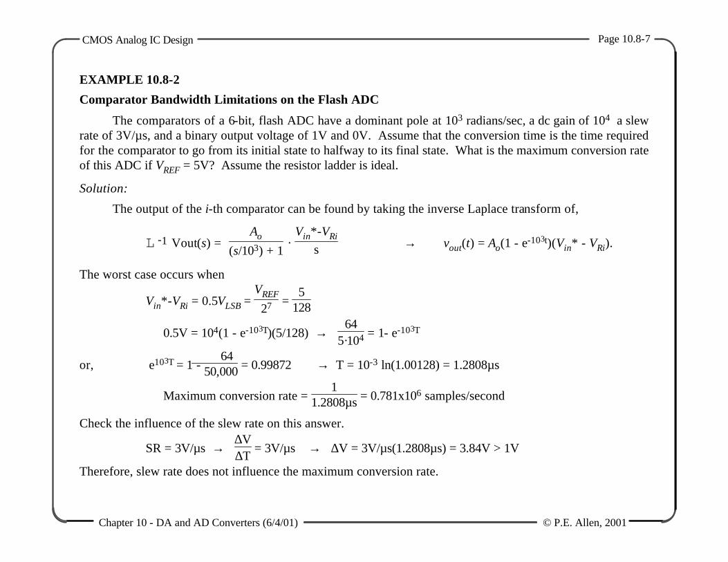
EXAMPLE 10.8-2
Comparator Bandwidth Limitations on the Flash ADC
The comparators of a 6-bit, flash ADC have a dominant pole at 103 radians/sec, a dc gain of 104 a slew rate of 3V/µs, and a binary output voltage of 1V and 0V. Assume that the conversion time is the time required for the comparator to go from its initial state to halfway to its final state. What is the maximum conversion rate of this ADC if VREF = 5V? Assume the resistor ladder is ideal.
Solution:
The output of the i-th comparator can be found by taking the inverse Laplace transform of,
L -1
Vout(s) =
Ao
(s/103) + 1·
Vin*-VRi
s → vout(t) = Ao(1 - e-103t)(Vin* - VRi).
The worst case occurs when
Vin*-VRi = 0.5VLSB = VREF
27 = 5
128
∴ 0.5V = 104(1 - e-103T)(5/128) → 64
5·104 = 1- e-103T
or, e103T = 1 - 64
50,000 = 0.99872 → T = 10-3 ln(1.00128) = 1.2808µs
∴ Maximum conversion rate = 1
1.2808µs = 0.781x10⁶ samples/second
Check the influence of the slew rate on this answer.
SR = 3V/µs → ∆V∆T
= 3V/µs → ∆V = 3V/µs(1.2808µs) = 3.84V > 1V
Therefore, slew rate does not influence the maximum conversion rate.

CMOS Analog IC Design Page 10.8-8
Chapter 10 - DA and AD Converters (6/4/01) © P.E. Allen, 2001
OTHER ERRORS OF THE PARALLEL ADC
• Resistor string error - if current is drawn from the taps to the resistor string this will create a “bowing” effect on the voltage. This can be corrected by applying the correct voltage to various points of the resistor string.
• Input common mode range of the comparators - the comparators at the top of the string must operate with the same performance as the comparators at the bottom of the string.
• Kickback or flashback - influence of rapid transition changes occuring at the input of a comparator. Can be solved by using a preamplifier or buffer in front of the comparator.
• Metastability - uncertainty of the comparator output causing the transition of the thermometer code to not be distinct.

CMOS Analog IC Design Page 10.8-9
Chapter 10 - DA and AD Converters (6/4/01) © P.E. Allen, 2001
INTERPOLATING ANALOG-DIGITAL CONVERTERS
A 3-bit interpolating ADC using a factor of 4
interpolation: Comments:
• Loading of the input is reduced from 8 comparators to two amplifiers.
• The outputs of the two amplifiers, V1 and V2, are interpolated through the resistor string and applied to the comparators.
• Because of the amplification of the input amplifiers and a single threshold, the comparators can be simple and are often replaced by a latch.
• If the dots in Fig. 10.8-4 are not equally spaced, INL and DNL will result.

CMOS Analog IC Design Page 10.8-10
Chapter 10 - DA and AD Converters (6/4/01) © P.E. Allen, 2001
• The comparators no longer need a large ICMR

CMOS Analog IC Design Page 10.8-11
Chapter 10 - DA and AD Converters (6/4/01) © P.E. Allen, 2001
A 3-BIT INTERPOLATING ADC WITH EQUALIZED COMPARATOR DELAYS
One of the problems in voltage (passive) interpolation is that the delay from the amplifier output to each comparator can be different due to different source resistance.
Solution:

CMOS Analog IC Design Page 10.8-12
Chapter 10 - DA and AD Converters (6/4/01) © P.E. Allen, 2001
FOLDING ANALOG-DIGITAL CONVERTERS
Allows the number of comparators to be reduced below the value of 2N-1.
Architecture for a folded ADC:
Operation:
The input is split into two or more parallel paths.
• First path uses a coarse quantizer to quantize the signal into 2n1 values
• The second path maps all of the 2n1 subranges onto a single subrange and applies this analog signal to a fine quantizer of 2n2 subranges.
Thus, the total number of comparators is 2n1-1 + 2n2-1 compared with 2n1+n2-1 for a parallel ADC.
I.e., if n1 = 2 and n2 = 4, the folding ADC requires 3 + 15 = 18 compared with 63 comparators.

CMOS Analog IC Design Page 10.8-13
Chapter 10 - DA and AD Converters (6/4/01) © P.E. Allen, 2001
FOLDING PREPROCESSOR
Illustration:
Comments:
• Folding is done simultaneously or in parallel so that only one clock cycle is needed for conversion.
• Folding will tend to increase the bandwidth of the analog input by a factor of F.
• Folding can reduce the power consumption and require less chip area.

CMOS Analog IC Design Page 10.8-14
Chapter 10 - DA and AD Converters (6/4/01) © P.E. Allen, 2001
EXAMPLE OF A FOLDING PREPROCESSOR
Folding characteristic for n1 = 2 and n2 = 3.
Problems:
• The sharp discontinuities of the folder are difficult to implement at high speeds.
• Fine quantizer must work at voltages ranging from 0 to VREF/4 (subranging).

CMOS Analog IC Design Page 10.8-15
Chapter 10 - DA and AD Converters (6/4/01) © P.E. Allen, 2001
MODIFIED FOLDING PREPROCESSORS
The above problems can be removed by the following folding preprocessors:

CMOS Analog IC Design Page 10.8-16
Chapter 10 - DA and AD Converters (6/4/01) © P.E. Allen, 2001
A 5-BIT FOLDING ADC USING 1-BIT QUANTIZERS (COMPARATORS)
Block diagram:
Comments:
• Number of comparators is 7 for the fine quantizer and 3 for the course quantizer for 10 total
• The zero crossings of the folders must be equally spaced to avoid linearity errors
• The number of folders can be reduced and the comparators simplified by use of interpolation

CMOS Analog IC Design Page 10.8-17
Chapter 10 - DA and AD Converters (6/4/01) © P.E. Allen, 2001
FOLDING CIRCUITS
Implementation of a times 4 folder:
Comments:
• Horizontal shifting is achieved by modifying the topmost and bottom resistors of the resistor string
• Folding and interpolation ADCs offer the most resolution at high speeds (˜ 8 bits at 200MHz)

CMOS Analog IC Design Page 10.8-18
Chapter 10 - DA and AD Converters (6/4/01) © P.E. Allen, 2001
SUMMARY OF INTERPOLATING AND FOLDING ADCs
Advantages of Interpolation:
• Large area and power reduction
• Input capacitance reduced
• Folder offset errors are averaged among interpolated signals
Comments on Resistive Interpolation:
• Low resistance is required for high speed implies high drive required from previous folding circuit
• Guaranteed monotonicity of phase shift
Comments on Active Interpolation:
• Subject to additional offsets (fine active interpolation not recommended)
• Lower drive necessary from initial folding circuits than for resistive interpolation

CMOS Analog IC Design Page 10.8-19
Chapter 10 - DA and AD Converters (6/4/01) © P.E. Allen, 2001
USE OF A S/H IN FRONT OF THE FOLDING ADC
Benefit of a S/H:
• With no S/H, the folding circuit acts as an amplitude-dependent frequency multiplier.
BW of ADC ≥ BW of Folding Circuit
• With S/H, all inputs to the folding circuit arrive at the same time.
- Therefore the folding circuit is no longer an amplitude-dependent frequency multiplier
- BW of the ADC is now limited by the BW of the S/H circuit
- Settling time of the folding and interpolating preprocessor is critical
Single S/H versus Distributed S/H:
• Single S/H requires high dynamic range for low THD
• Dynamic range requirement for distributed S/H reduced by a factor equal to the number of S/H stages
• If the coarse quantizer uses the same distributed S/H signals as the fine preprocessor, the coarse/fine synchronization is automatic
• The clock skew between the distributed S/H stages must be small. The clock jitter will have a greater effect on the distributed S/H approach.
Including a Preamplifier in the S/H circuit:
• Reduces the effect of folding circuit input offset and comparator input offset
• For a S/H distributed over D stages, then:
- The preamp linear range requirement is the input range/D (all subsequent interpolated signals use this range)
- The preamp input common mode range is the input range

CMOS Analog IC Design Page 10.8-20
Chapter 10 - DA and AD Converters (6/4/01) © P.E. Allen, 2001
- The preamp output common mode range is small which implies the switch nonlinearity is not dependent on input signal amplitude

CMOS Analog IC Design Page 10.8-21
Chapter 10 - DA and AD Converters (6/4/01) © P.E. Allen, 2001
ERROR SOURCES AND LIMITATIONS OF A BASIC FOLDING ADC
Error Sources:
• Offsets in reference voltages due to resistor mismatch
• Preamp offset (reduced by large input devices for low VGS-VT, with common-centroid geometry)
• vin feedthrough to reference ladder via Cgs of input pairs loading the input places a maximum value on ladder resistance which is dependent on the input frequency. Also, the no. of preamp/folder circuits loading the input must be minimized.
• Folder current-source mismatches (gives signal-dependent error⇒distortion)
• Comparator kickback (driving nodes should be low impedance)
• Comparator metastability condition (uncertainty of comparator output)
• Misalignment between coarse and fine quantization outputs (large code errors are possible)
Sampling Speed Limitations:
• Folding output settling time
• Comparator settling time
• Clock distribution and layout
• Clock jitter
Input Bandwidth Limitations:
• Maximum folding signal frequency = (F/2)·fin, unless a S/H is used
• Preamplifier has a limited linear range and frequency dependent delay which gives distortion
• The folder has limited linear range and frequency dependent delay which gives distortion

CMOS Analog IC Design Page 10.8-22
Chapter 10 - DA and AD Converters (6/4/01) © P.E. Allen, 2001
• Parasitic capacitance of routing to comparators

CMOS Analog IC Design Page 10.8-23
Chapter 10 - DA and AD Converters (6/4/01) © P.E. Allen, 2001
MULTIPLE-BIT, PIPELINE ANALOG-DIGITAL CONVERTERS
A compromise between speed and resolution is to use a pipeline ADC with multiple bits/stage.
i-th stage of a k-bit per stage pipeline ADC with residue amplification:
Residue voltage = Vi-1 -
b1
2 + b2
22 + ··· + bk-1
2k-1 + bk
2k VREF

CMOS Analog IC Design Page 10.8-24
Chapter 10 - DA and AD Converters (6/4/01) © P.E. Allen, 2001
A 3-STAGE, 3-BIT PER STAGE PIPELINE ADC
Illustration of the operation:
Converted word is 011 111 001
Comments:
• Only 21 comparators are required for this 9-bit ADC
• Conversion occurs in three clock cycles
• The residue amplifier will cause a bandwidth limitation,
GB = 50MHz → f-3dB = 50MHz
23 ≈ 6MHz

CMOS Analog IC Design Page 10.8-25
Chapter 10 - DA and AD Converters (6/4/01) © P.E. Allen, 2001
SUBRANGING, MULTIPLE-BIT, PIPELINE ADCs
The residue amplifier can be replaced by dividing VREF to the next stage by 2k if the stage has k-bits.
Illustration of a 2-stage, 2-bits/stage pipeline ADC:
Comments:
• Resolution of the comparators for the following stages increases but fortunately, the tolerance of each stage decreases by 2k for every additional stage.
• Removes the frequency limitation of the amplifier

CMOS Analog IC Design Page 10.8-26
Chapter 10 - DA and AD Converters (6/4/01) © P.E. Allen, 2001
IMPLEMENTATION OF THE DAC IN THE MULTIPLE-BIT, PIPELINE ADC
Circuit:
Comments:
• A good compromise between area and speed
• The ADC does not need to be a flash or parallel if speed is not crucial
• Typical performance is 10 bits at 50Msamples/sec

CMOS Analog IC Design Page 10.8-27
Chapter 10 - DA and AD Converters (6/4/01) © P.E. Allen, 2001
EXAMPLE 10.8-3
Examination of error in subranging for a 2-stage, 2-bits/stage pipeline ADC
The stages of the 2-stage, 2-bits/stage pipeline ADC shown below are ideal. However, the second stage divides VREF by 2 rather than 4. Find the ±INL and ±DNL for this ADC.
Solution
Examination of the first stage shows that its output, Vout(1) changes at
Vin(1)VREF
= 14,
24,
34, and
44 .
The output of the first stage will be
Vout(1)VREF
= b1
2 + b2
4 .
The second stage changes at
Vin(2)VREF
= 18,
28,
38, and
48
where Vin(2) = Vin(1) - Vout(1).

CMOS Analog IC Design Page 10.8-28
Chapter 10 - DA and AD Converters (6/4/01) © P.E. Allen, 2001
The above relationships permit the infomation given in Table 10.8-1.

CMOS Analog IC Design Page 10.8-29
Chapter 10 - DA and AD Converters (6/4/01) © P.E. Allen, 2001
EXAMPLE 10.8-3 - CONTINUED
Table 10.8-1
Output digital word for Ex. 10.8-3
Vin(1)VREF
b1 b2 Vout(1)VREF
Vin(2)VREF
b3 b4 Ideal Ouput b1 b2 b3 b4
0 0 0 0 0 0 0 0 0 0 0 1/16 0 0 0 1/16 0 0 0 0 0 1 2/16 0 0 0 2/16 0 1 0 0 1 0 3/16 0 0 0 3/16 0 1 0 0 1 1 4/16 0 1 4/16 0 0 0 0 1 0 0 5/16 0 1 4/16 1/16 0 0 0 1 0 1 6/16 0 1 4/16 2/16 0 1 0 1 1 0 7/16 0 1 4/16 3/16 0 1 0 1 1 1 8/16 1 0 8/16 0 0 0 1 0 0 0 9/16 1 0 8/16 1/16 0 0 1 0 0 1 10/16 1 0 8/16 2/16 0 1 1 0 1 0 11/16 1 0 8/16 3/16 0 1 1 0 1 1 12/16 1 1 12/16 0 0 0 1 1 0 0 13/16 1 1 12/16 1/16 0 0 1 1 0 1 14/16 1 1 12/16 2/16 0 1 1 1 1 0 15/16 1 1 12/16 3/16 0 1 1 1 1 1
Comparing the actual digital output word with the ideal output word gives the following results: +INL = 0LSB, -INL = 0111-0101 = -2LSB, +DNL = (1000-0101) - 1LSB = +2LSB, and -DNL = (0101-0100) - 1LSB = 0LSB.

CMOS Analog IC Design Page 10.8-30
Chapter 10 - DA and AD Converters (6/4/01) © P.E. Allen, 2001
EXAMPLE 10.8-4
Accuracy requirements for the amplifier of a 2-stage, 2-bits/stage pipeline ADC
A 4-bit ADC consisting of two, 2-bit stages (pipes) is shown. Assume that the 2-bit ADC’s and the 2-bit DAC function ideally. Also, assume that VREF = 1V. The ideal value of the scaling factor, k, is 4. Find the maximum and minimum value of k that will not cause an error in the 4-bit ADC. Express the tolerance of k in terms of a plus and minus percentage.
Solution
The input to the second ADC is vin(2) = k
vin(1) -
b1
2 + b2
4 . Designating this voltage as v’in(2) when k
= 4, then the difference between vin(2) and v’in(2) must be less than ±1/8 or the LSB bits will be in error.
Therefore, vin(2) - v’in(2) =
k vin(1) - k
b1
2 + b2
4 - 4 vin(1) + 4
b1
2 + b2
4 ≤ 18
If k = 4 + ∆k, then
4 vin(1) + ∆k vin(1) - 4
b1
2 + b2
4 - ∆k
b1
2 + b2
4 - 4 vin(1) + 4
b1
2 + b2
4 ≤ 18
or ∆k
vin(1) -
b1
2 + b2
4 ≤ 18 .
The largest value of
vin(1) -
b1
2 + b2
4 is 1/4 for any value of vin(1) from 0 to VREF.

CMOS Analog IC Design Page 10.8-31
Chapter 10 - DA and AD Converters (6/4/01) © P.E. Allen, 2001
Therefore, ∆k4 ≤
18 ⇒ ∆k ≤ 1/2. The tolerance of k is
∆kk =
±12·4 =
±18 ±12.5%

CMOS Analog IC Design Page 10.8-32
Chapter 10 - DA and AD Converters (6/4/01) © P.E. Allen, 2001
EXAMPLE OF A MULTIPLE-BIT, PIPELINE ADC
Two-stages with 5-bits per stage resulting in a 10-bit ADC with a sampling rate of 5Msamples/second.
Architecture:
Features:
• Requires only 2n/2-1 comparators
• LSBs decoded using 31 preset charge redistribution capacitor arrays
• Reference voltages used in the LSBs are generated by the MSB ADC
• No op amps are used

CMOS Analog IC Design Page 10.8-33
Chapter 10 - DA and AD Converters (6/4/01) © P.E. Allen, 2001
EXAMPLE OF A MULTIPLE-BIT, PIPELINE ADC - CONTINUED
MSB Conversion:
Operation:
1.) Sample Vin* on each 32C capacitance autozeroing the comparators

CMOS Analog IC Design Page 10.8-34
Chapter 10 - DA and AD Converters (6/4/01) © P.E. Allen, 2001
2.) Connect each comparator to a node of the resistor string generating a thermometer code.
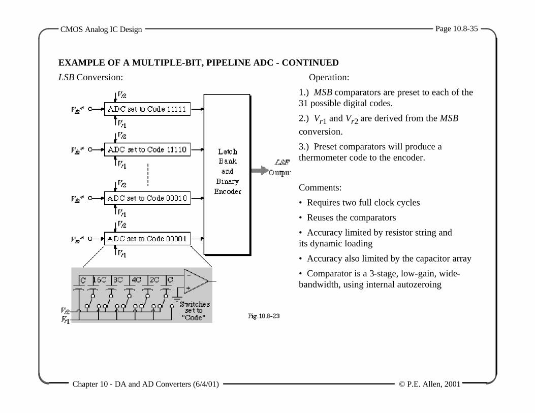
CMOS Analog IC Design Page 10.8-35
Chapter 10 - DA and AD Converters (6/4/01) © P.E. Allen, 2001
EXAMPLE OF A MULTIPLE-BIT, PIPELINE ADC - CONTINUED
LSB Conversion: Operation:
1.) MSB comparators are preset to each of the 31 possible digital codes.
2.) Vr1 and Vr2 are derived from the MSB conversion.
3.) Preset comparators will produce a thermometer code to the encoder.
Comments:
• Requires two full clock cycles
• Reuses the comparators
• Accuracy limited by resistor string and its dynamic loading
• Accuracy also limited by the capacitor array
• Comparator is a 3-stage, low-gain, wide-bandwidth, using internal autozeroing

CMOS Analog IC Design Page 10.8-36
Chapter 10 - DA and AD Converters (6/4/01) © P.E. Allen, 2001
DIGITAL ERROR CORRECTION
The multiple-bit, pipeline ADC architecture permits the correction of digital errors that occur in the previous stage.
The problem (Comparator in 1st stage has an error): The solution (use an additional bit for correction):
For an input of 0.4VREF the output should be 0110.
Comments:
• The idea is to add a correcting bit to the following stage to correct for errors in the previous stage.
• The subranging or amplification of the next stage does not include the correcting bit.
• Correction can be done after all stages of the pipeline ADC have converted or after each individual stage.

CMOS Analog IC Design Page 10.8-37
Chapter 10 - DA and AD Converters (6/4/01) © P.E. Allen, 2001
EXAMPLE OF A PIPELINE ADC WITH DIGITAL ERROR CORRECTION
ADC uses 4 stages of 4-bits each and employs a successive approximation ADC to get 13-bit resolution at 250 ksamples/sec.
Block diagram of a 13-bit pipeline ADC:
S/H +
-
S/H+
-
ADC-N1 bit DAC-N1 bit
S/H+
-
ADC-N2 bit DAC-N2 bit ADC-N3 bit DAC-N3 bit
Vin
2N2 2N32N1
S/H
N1 bit REG
N3 bit REG
N2 bit REG
N1 bit REG
N2 bit REG
N1 bit REG
0.5 LSB offset 0.5 LSB offset
VREF
3 bits
3 bits
3 bits
4 bits
Comments:
• The ADC of the first stage uses 16 equal capacitors instead of 4 binary weighted for more accuracy
• One bit of the last three stages is used for error correction.

CMOS Analog IC Design Page 10.8-38
Chapter 10 - DA and AD Converters (6/4/01) © P.E. Allen, 2001
12-BIT PIPELINE ADC WITH DIGITAL ERROR CORRECTION & SELF-CALIBRATION†
Digital Error Correction:
• Avoids saturation of the next stage • Reduces the number of missing codes • Relaxed specifications for the comparators • Compensates for wrong decisions in the coarse quantizers
Self-Calibration:
• Can calibrate the effects of the DAC nonlinearity and gain error
† J. Goes, et. al., CICC’96

CMOS Analog IC Design Page 10.8-39
Chapter 10 - DA and AD Converters (6/4/01) © P.E. Allen, 2001
• Can be done by digital or analog methods or both

CMOS Analog IC Design Page 10.8-40
Chapter 10 - DA and AD Converters (6/4/01) © P.E. Allen, 2001
TIME-INTERLEAVED ANALOG-DIGITAL CONVERTERS
Slower ADCs are used in parallel.
Illustration:
Comments:
• Can get the same throughput with less chip area
• If M = N, then a digital word is converted at every clock cycle
• Multiplexer and timing become challenges at high speeds

CMOS Analog IC Design Page 10.8-41
Chapter 10 - DA and AD Converters (6/4/01) © P.E. Allen, 2001
SUMMARY OF REPORTED HIGH-SPEED ADCs
Recently published high-speed, CMOS ADCs.
Architecture [paper reference]
Sampling Freq. (Msps)
Signal Freq. (MHz)
ENOB1 (bits)
Power (mW)
Active Area (mm2)
Feature Size2 (µm)
Vin (Vp-p) VDD (V)
Folding+ Interpolating [1] 70 8 5.5 110 0.7 0.8 2.0 5.0
Flash [2] 200 100 5.0 400 2.7 0.6 - -
Flash [3] 200 20 6.0 110 1.6 0.5 0.3 3.0
Flash w. pre-processing [4] 175 84 4.0 160 12.0 0.7 1.2 3.3
Folding+ Interpolating [5] 125 10 5.5 225 4.0 1.0 - 5.0
Folding+ Interpolating [6] 80 75 5.8 80 0.3 0.5 1.6 3.3
Subranging+Interleaving [7] 95 50 8.0 1100 50.0 1.0 2.0 5.0
References for Recently Published High-Speed CMOS ADCs [1] B. Nauta and A. Venes, “A 70Ms/s 110mW 8-b CMOS Folding and Interpolating A/D Converter, IEEE J. of Solid-State
Circuits, vol. 30, no. 12, Dec. 1995, pp. 1302-1308.
[2] J. Spalding and D. Dalton, “A 200 Msample/s 6b Flash ADC in 0.6µm CMOS,” Proc. of ISSCC, paper SA19.5, 1996.
[3] S. Tsukamoto, I. Dedic, et. al., “A CMOS 6b 200Msamples/s 3V-supply A/D converter for a PRML Read Channel LSI,” Proc. of ISSCC, paper TP4.5, 1996.
[4] R. Roovers and M. Steyaert, “A 175Ms/s, 6-b, 160mW, 3.3V CMOS A/D Converter,” IEEE J. of Solid-State Circuits, vol. 31, no. 7, July 1996, pp. 938-944.
[5] M. Flynn and D. Allstot, “CMOS Folding A/D Converters with Current-Mode Interpolation,” IEEE J. of Solid-State Circuits, vol. 31, no. 9, Sept. 1996, pp. 1248-1257.
[6] A. Venes and R. van de Plassche, “An 80 MHz, 80mW, 8-b CMOS Folding A/D Converter with Distributed Track-and-Hold Preprocessing,” IEEE J. of Solid-State Circuits, vol. 31, no. 12, Dec. 1996, pp. 1846-1853.

CMOS Analog IC Design Page 10.8-42
Chapter 10 - DA and AD Converters (6/4/01) © P.E. Allen, 2001
[7] K. Kim, N. Kusayanagi, and A. Abidi, “A 10-b, 100-Ms/s CMOS A/D Converter,” IEEE J. of Solid-State Circuits, vol. 32, no. 3, Mar. 1997, pp. 302-311.

CMOS Analog IC Design Page 10.8-43
Chapter 10 - DA and AD Converters (6/4/01) © P.E. Allen, 2001
SUMMARY OF HIGH-SPEED ANALOG-DIGITAL CONVERTERS
Type of ADC Primary Advantage Primary Disadvantage
Flash or parallel Fast Area is large if N > 6
Interpolating Fast Requires accurate interpolation
Folding Fast Bandwidth increases if no S/H used
Multiple-Bit, Pipeline Increased number of bits Slower than flash
Time-interleaved Small area with large throughput Precise timing and fast multiplexer
Typical Performance:
• 6-8 bits
• 200-500 Msamples/sec.
• The ENOB at the Nyquist frequency is typically 1-2 bits less that the ENOB at low frequencies.
• Power is approximately 0.3 to 1W