1 the pn-junction in equilibrium 2 the i–v characteristics
TRANSCRIPT
Introduction to Microelectronics1
PN-JUNCTION
1 The PN-junction in Equilibrium
2 The I–V Characteristics of the PN-Junction
3 Deviations from the Ideal Diode
Introduction to Microelectronics
2
−
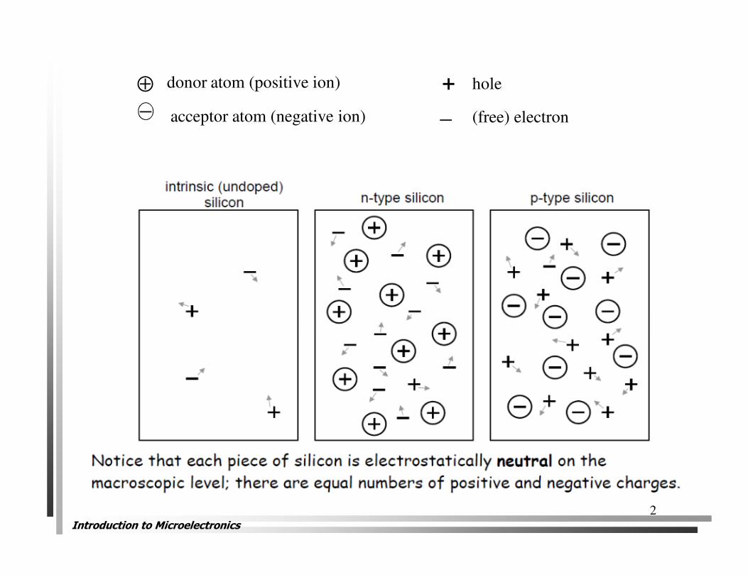
⊕ donor atom (positive ion)
− acceptor atom (negative ion)
+ hole
(free) electron
Introduction to Microelectronics
3
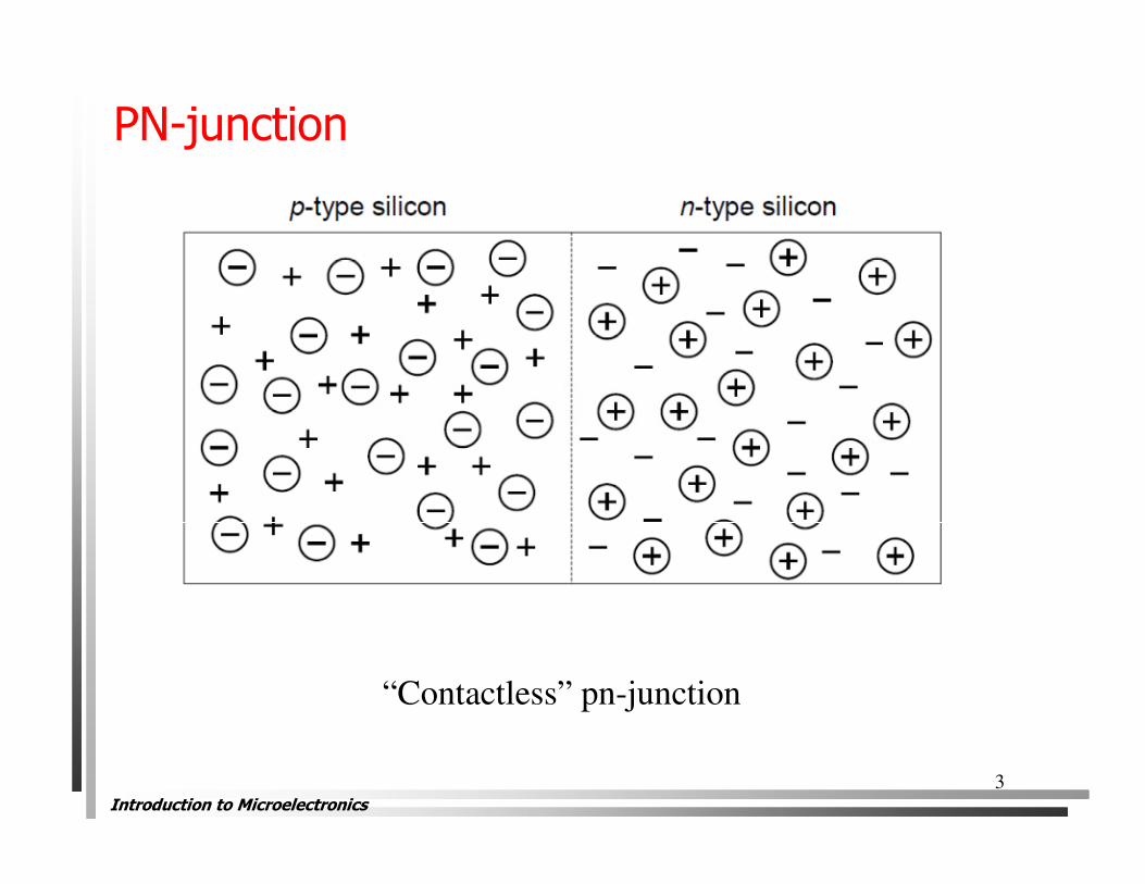
PN-junction
“Contactless” pn-junction

Introduction to Microelectronics4
1016
1014
1012
1010
106
108
104
102
nn = ND
pp = NA
np = ni2 / NA pn = ni
2/ ND
N A=1016
cm-3
PN D=10
15cm
-3
N
ohmic
contact
ohmic
contact
A B
-N A
N D
x(a) Step junction
(b) “initial” carrier concentrations
ni=1010cm-3
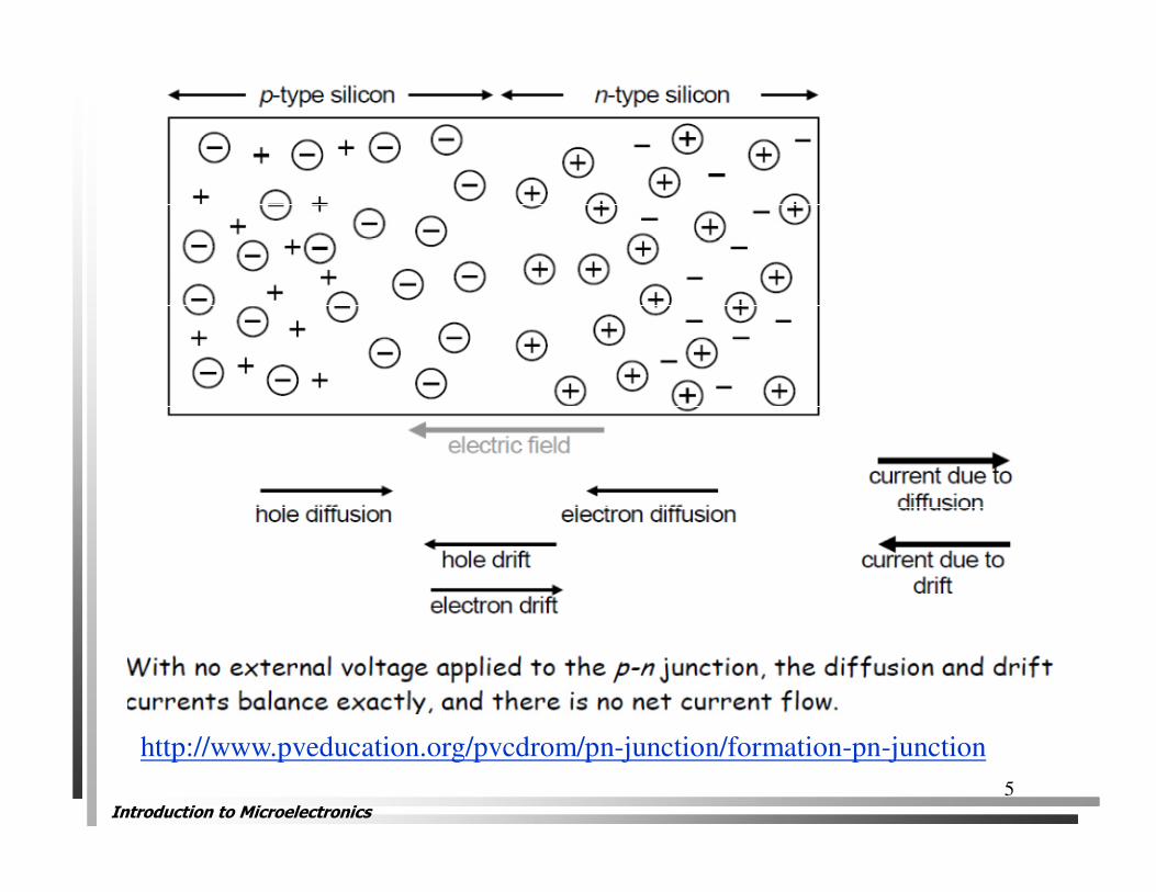
“Before contacting”, the two
regions are electrically neutral
( ρ = 0 ).
Introduction to Microelectronics
5
http://www.pveducation.org/pvcdrom/pn-junction/formation-pn-junction
Introduction to Microelectronics6
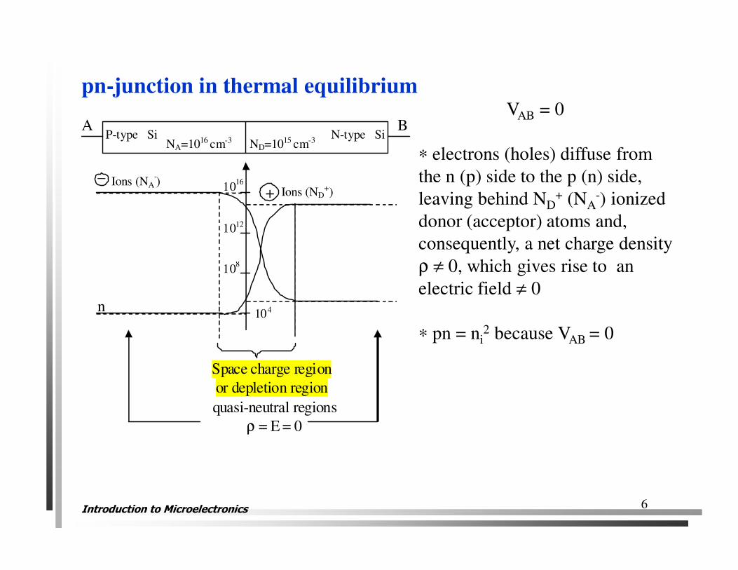
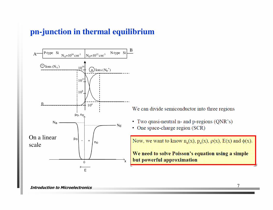
NA=1016 cm-3 ND=1015 cm-3 P-type Si N-type Si
A B
1016
1012
108
104 n
Space charge region
or depletion region
quasi-neutral regions
ρ = E = 0
Ions (NA-)
Ions (ND+) +
_
VAB = 0
∗ electrons (holes) diffuse from
the n (p) side to the p (n) side,
leaving behind ND+ (NA
-) ionized
donor (acceptor) atoms and,
consequently, a net charge density
ρ ≠ 0, which gives rise to an
electric field ≠ 0
∗ pn = ni2 because VAB = 0
pn-junction in thermal equilibrium
Introduction to Microelectronics7
NA=1016 cm-3 ND=1015 cm-3 P-type Si N-type Si A
B
1016
1012
108
104 n
Ions (NA-)
Ions (ND+) +
_
pn-junction in thermal equilibrium
On a linear
scale
Introduction to Microelectronics8

Introduction to Microelectronics9
Introduction to Microelectronics
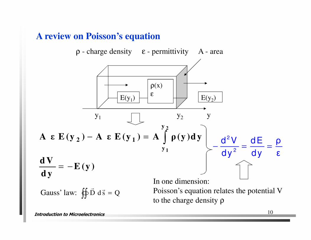
A review on Poisson’s equation
E(y1)
ρ(x)
εE(y2)
ρ - charge density ε - permittivity A - area
y1 y2 y
2
1
y
2 1
y
A ε E (y ) A ε E (y ) A ρ (y )d y
d VE (y )
d y
− =
= −
∫ 2
2
d V dE ρ
dy dy ε− = =
Qsd D =∫∫�
�
Gauss’ law:
In one dimension:
Poisson’s equation relates the potential V
to the charge density ρ
10
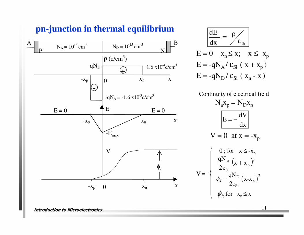
Introduction to Microelectronics11
EE = 0 E = 0
-xp xn
-Emax
-xp xn
-qNA = -1.6 x10⁻³
c/cm3
x
x
1.6 x10-4
c/cm3qND
ρ (c/cm )
+
-0
x
φJ
xn-xp 0
V
Siερ
dx
dE=
E = 0 xn ≤ x; x ≤ -xp
E = -qNA / εSi ( x + xp )
E = -qND / εSi ( xn - x )
Continuity of electrical field
Naxp = NDxn
dx
dVE −=
V = 0 at x = -xp
( )2
p
Si
A xx2ε
qN+
( )2D
n
Si
qNx-x
2εJφ −
0 ; for x ≤ -xp
V =
φJ; for xn ≤ x
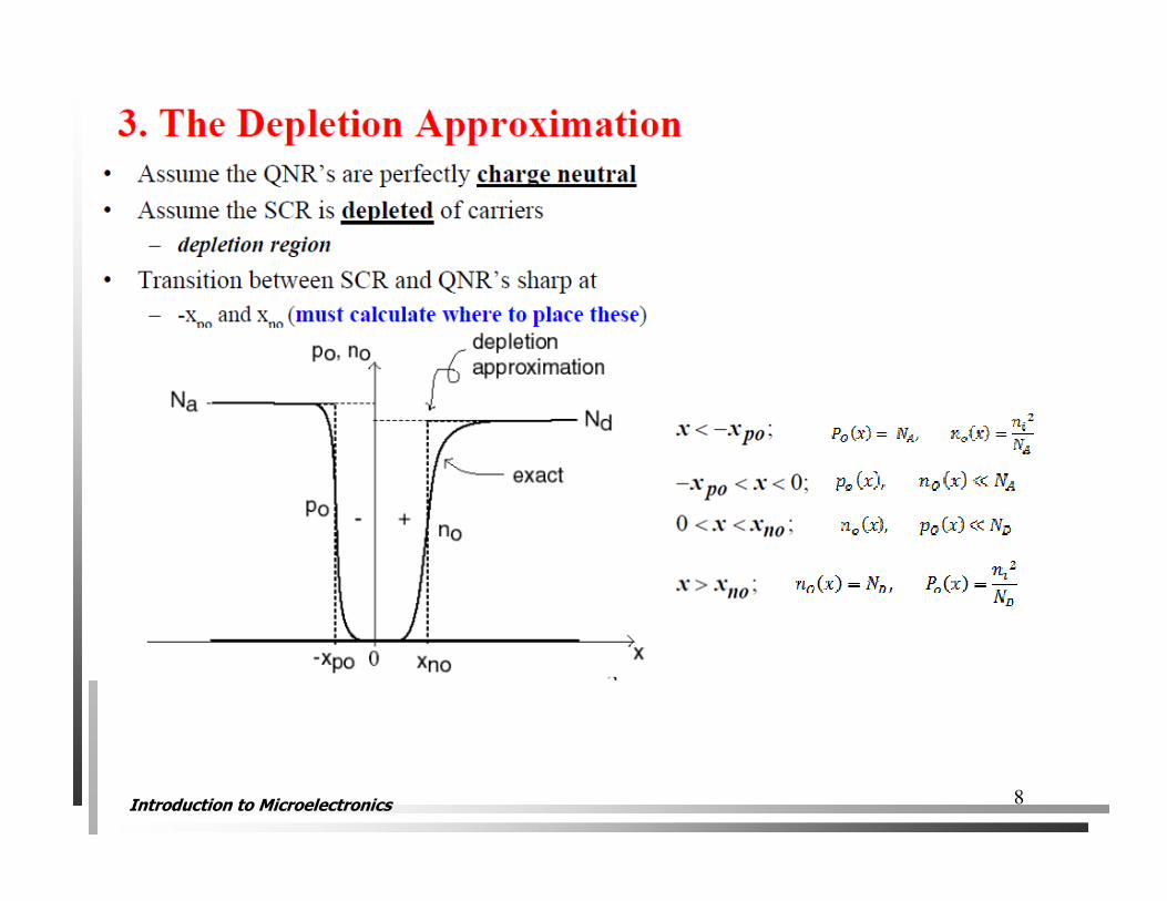
pn-junction in thermal equilibrium
3
P- NNA = 10
16 cm
-3 ND = 1015
cm-3A B
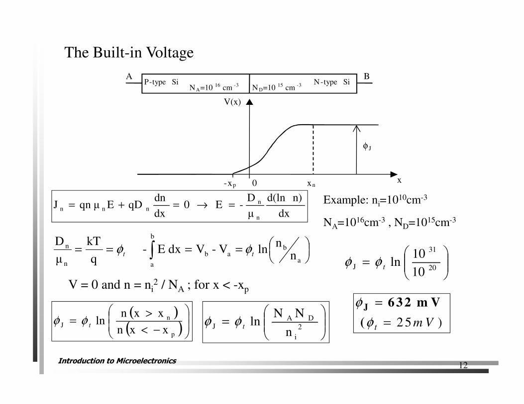
Introduction to Microelectronics
dx
n) d(ln
µ
D- E 0
dx
dnqDEqn µJ
n
nnnn =→=+=
==== ∫
a
bab
b
an
n
nn
ln V-V dx E- q
kT
µ
Dtt φφ
( )( )
−<
>=
p
nJ
xxn
xxnln tφφ
V = 0 and n = ni2 / NA ; for x < -xp
=
2
i
DAJ
n
NNln tφφ
=
20
31
J10
10ln tφφ
2 5 )
J 6 3 2 m V
( t m V
φ
φ
=
=
NA=10 16 cm -3 N D=10 15 cm -3P-type Si N-type Si
φ J
xn0-xpx
V(x)
A B
The Built-in Voltage
Example: ni=1010cm-3
NA=1016cm-3 , ND=1015cm-3
12
Introduction to Microelectronics
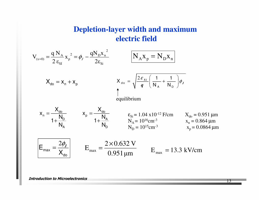
Depletion-layer width and maximum
electric field
Si
2
nD2
p
SI
A0)(x
2ε
xqNx
ε 2
N qV −=== Jφ
2d o
A D
1 1X
N N
S i
Jq
εφ
= +
don
D
A
Xx
N1
N
=
+
dop
A
D
Xx
N1
N
=
+
nDpA xNxN =
do n pX x x= +
equilibrium
εSi = 1.04 x10⁻¹² F/cm Xdo = 0.951 µm
NA = 1016cm-3 xn = 0.864 µm
ND = 1015cm-3 xp = 0.0864 µm
2max
do
EX
Jφ=
µm 0.951
V 0.6322Emax
×= kV/cm 13.3E max =
13

Introduction to Microelectronics
P- NNA = 10
16 cm
-3 ND = 1016
cm-3A B
14

Introduction to Microelectronics
P- NNA = 1016 cm-3 ND = 10
17cm
-3A B
15

Introduction to Microelectronics16
Introduction to Microelectronics17
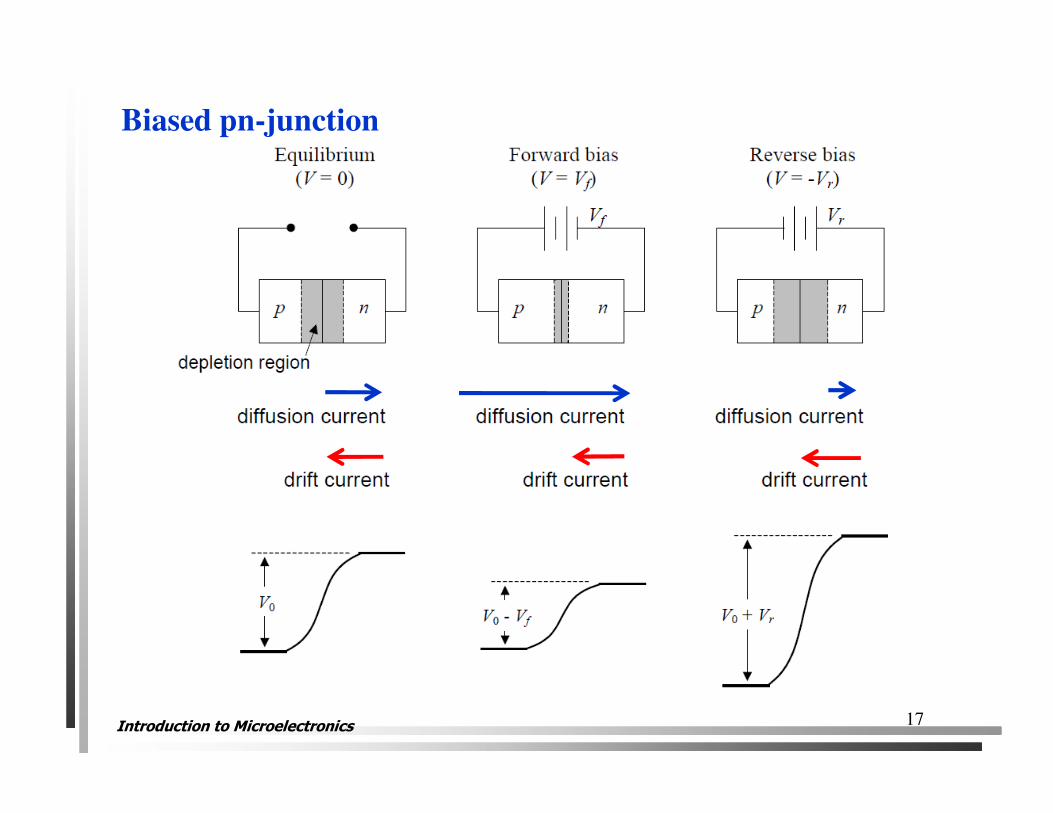
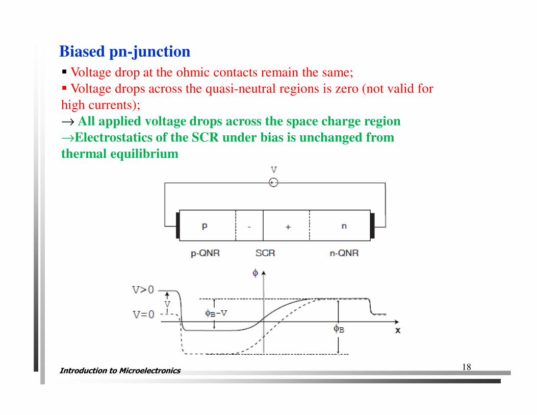
Biased pn-junction
Introduction to Microelectronics18
Biased pn-junction
� Voltage drop at the ohmic contacts remain the same;
� Voltage drops across the quasi-neutral regions is zero (not valid for
high currents);
→ All applied voltage drops across the space charge region
→Electrostatics of the SCR under bias is unchanged from
thermal equilibrium
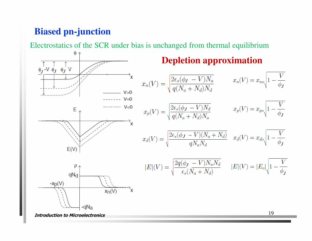
Introduction to Microelectronics19
Biased pn-junction
Electrostatics of the SCR under bias is unchanged from thermal equilibrium
Depletion approximation
J
J
J
J
J
J
J
J
J JJ
Introduction to Microelectronics
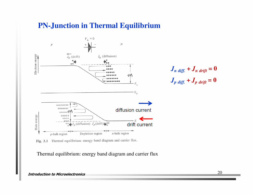
PN-Junction in Thermal Equilibrium
Jn diff. + Jn drift = 0
Jp diff. + Jp drift = 0
20
Thermal equilibrium: energy band diagram and carrier flux
qφJ
qφJ
Introduction to Microelectronics
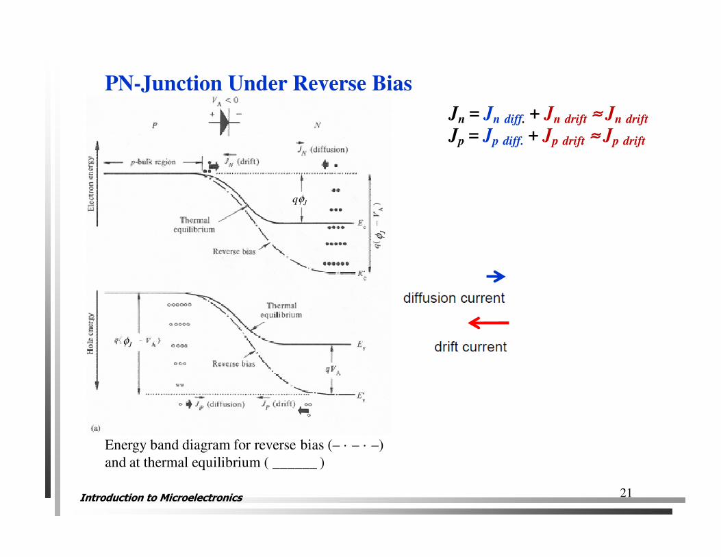
PN-Junction Under Reverse Bias
Energy band diagram for reverse bias (– · – · –)
and at thermal equilibrium ( ______ )
Jn = Jn diff. + Jn drift ≈≈≈≈ Jn drift
Jp = Jp diff. + Jp drift ≈≈≈≈ Jp drift
21
qφJ
φJ
φJ

Introduction to Microelectronics
Jn = Jn diff. + Jn drift ≈≈≈≈ Jn diff.
Jp = Jp diff. + Jp drift ≈≈≈≈ Jp diff.
J = Jn + Jp
VA > 0
The voltage drop across the
(quasi)-neutral regions
is ≈ zero for low-level
injection
PN-Junction Under Forward Bias
22
φJ
φJ
Energy band diagram for forward bias (– · – · –) and
at thermal equilibrium ( )

Introduction to Microelectronics23
I
VA
IDO – current downhill α p ( N-side )
P N
φJ
-xp xn
Equilibrium
(VA=0)
M. Born, Atomic Physics, Dover, p. 305
R. Feynman et al., The Feynman Lectures on Physics, Addison
Wesley, vol. 3, p. 14.8.
Hole current
A few holes on the P-side approach the
barrier with enough energy to carry over it
and reach the N-side, where they
recombine
IUP – current uphill α NA exp(-φJ / φt )
(same reasoning for electrons)
IUP is balanced by a continual generation of pairs
by thermal fluctuations near the junction on the
N-side and some of the holes produced fall
down the energy gradient into the P-side giving a current IDO
Equilibrium: IUP = IDO = IS α NA exp(-φJ / φt )
Boltzmann
First order model: IDO is independent of VA – the rate of thermal generation of pairs will not
change for VA ≠≠≠≠0 since it depends only on local properties of the crystal near the junction.
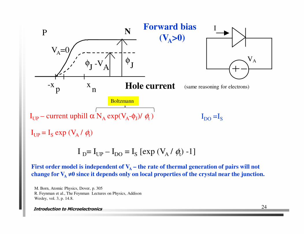
Introduction to Microelectronics24
I
VA
IDO =IS
Forward bias
(VA>0)
M. Born, Atomic Physics, Dover, p. 305
R. Feynman et al., The Feynman Lectures on Physics, Addison
Wesley, vol. 3, p. 14.8.
Hole current
IUP – current uphill α NA exp(VA-φJ)/ φt )
(same reasoning for electrons)
Boltzmann
First order model is independent of VA – the rate of thermal generation of pairs will not
change for VA ≠≠≠≠0 since it depends only on local properties of the crystal near the junction.
P N
φJφ
J -VA
-xp
VA=0
xn
IUP = IS exp (VA / φt)
I D= IUP – IDO = IS [exp (VA / φt) -1]

Introduction to Microelectronics
25
At the edges of the depletion region, -xp and
xn, equilibrium conditions do not prevail so
we must use the "law of the junction".
Development of analytical dc model (I-V characteristics)
of the diode I
VA
( )( )
( ) ( )
( )( )
( ) ( ) ( )exp
exp exp
exp
p np A J
n
p np A
n
t
J
t
q x xp x
q x x
V
p x
n x V
n x k
T
T
k
− −− − − = − =
− −− − = =
φ φφ φφ φφ φ φφφφ
φφφφ
φ φφ φφ φφ φ φφφφ
φφφφ
A B
NAP ND
-xp xn
QNRQNR
0
N
φJφ
J - VA
-xp
VA=0
xn
φJ
φJ
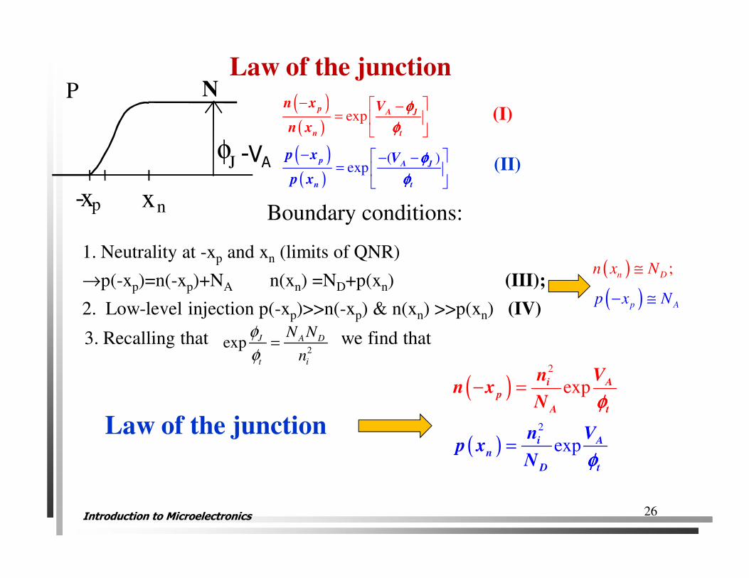
Introduction to Microelectronics26
Law of the junctionP N
φJ
-xp xn
-VA
( )
( )
;
− ≅
≅
A
n D
pp x
n N
N
x
Boundary conditions:
3. Recalling that we find that 2
exp =J A D
t i
N N
n
φ
φ
( )
( )2
2
e
xp
x
e
pi A
p
A t
i A
n
D t
n Vn
n Vp x
N
N
x
φφφφ
φφφφ− =
=Law of the junction
( )( )
( )( )
( )exp
exp
p
p A J
n t
A J
n t
p x V
p x
n x V
n x
φφφφ
φφφφ
φφφφ
φφφφ
−
− −=
− −=
1. Neutrality at -xp and xn (limits of QNR)
→p(-xp)=n(-xp)+NA n(xn) =ND+p(xn) (III);
2. Low-level injection p(-xp)>>n(-xp) & n(xn) >>p(xn) (IV)
(I)
(II)
Introduction to Microelectronics27
( )
( )
;
− ≅
≅
A
n D
pp x
n N
N
x
Boundary conditions for minority carriers
( )2
expi A
p
A t
n Vn x
N− =
φφφφ
Law of the junction
A B
NAP ND
-xp xn
QNRQNR
0
N
-Wp Wn
( )2
i
p
A
nn W
N− = ( )
2
i
n
D
np W
N=
( )2
expi An
D t
n Vp x
N=
φφφφ
Ohmic contacts:
Thermal equilibrium

Introduction to Microelectronics28
Calculate the current-voltage characteristic of a “short” P+N junction diode
I
VA
1. Holes are the main carriers;
2. Recombination is negligible in the N region;
3. Diffusion current is dominant
( )2
expi A
n
D t
n Vp x
N φ=
NAND
0 xn Wn
( )2
i
n
D
np W
N=
Law of the
junction
Ohmic
contact
( ) ( )
( )
2
exp 1
n n
p p p
n n
i A
p p p
n Dn t
p W p xdpJ qD qD
dx W x
n VI AJ qAD
W Nx φ
−= − = −
−
= = −
−
2
1 ;φ
≅ = −
≅
A
t
V
p S
i
S p
n D
I I I e
nI qAD
W N
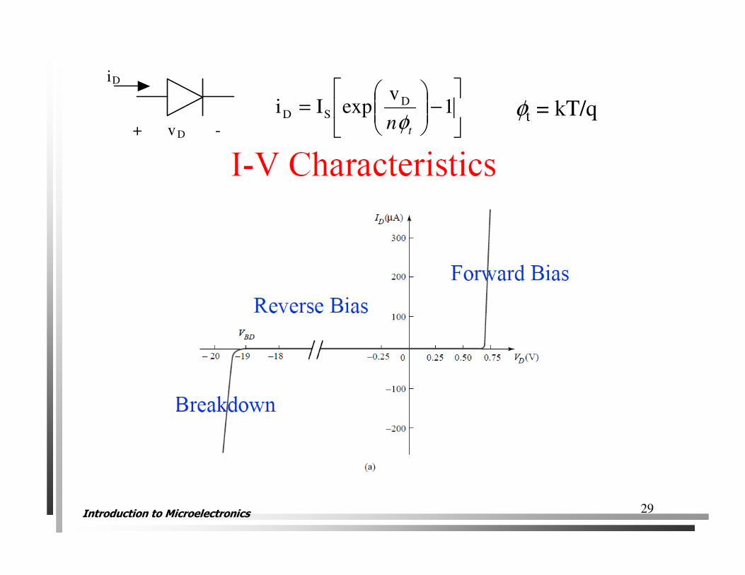
Introduction to Microelectronics29
+ vD -
iD
−
= 1
vexpIi D
SD
tnφφt = kT/q
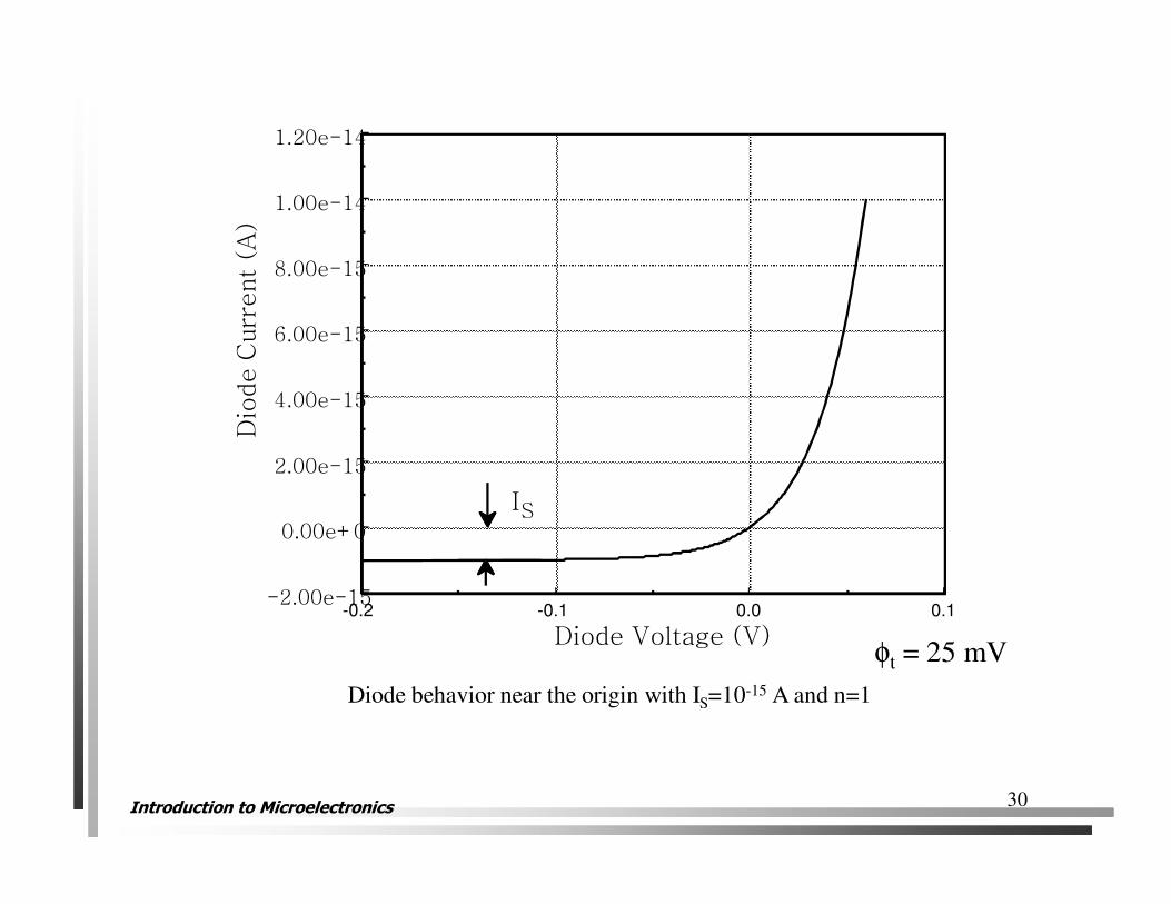
Introduction to Microelectronics30
0.10.0-0.1-0.2-2.00e-15
0.00e+0
2.00e-15
4.00e-15
6.00e-15
8.00e-15
1.00e-14
1.20e-14
Diode Voltage (V)
Dio
de C
urr
ent
(A)
IS
Diode behavior near the origin with IS=10-15 A and n=1
φt = 25 mV

Introduction to Microelectronics31
Diode Voltage (V)
1.00.90.80.70.60.50.40.30.20.10.010 -15
10 -14
10 -13
10 -12
10 -11
10 -10
10 -9
10 -8
10 -7
10 -6
10 -5
10 -4
10 -3
10 -2
10 -1
Dio
de C
urr
ent
(A)
φt = 0.025 V
Slope - 1 decade/60 mV
I = 10 AS
-15
Diode i -v characteristic on semilog scale
IS : saturation current
n : ideality factor ( 1 to 2 )
φt : kT/q
k : 1.38 x10⁻²³ J/K
Typical values of IS:
10-18 A ≤ IS ≤ 10-9 A
−
= 1
vexpIi D
SD
tnφ
+ vD -
iD
Introduction to Microelectronics
32
References
– EEL 7061 Eletrônica Básicahttp://www.lci.ufsc.br/electronics/index7061.htm
– Reid R. Harrison, “Analog Integrated Circuit Design” ECE/CS 5720/6720 Department of Electrical and Computer Engineering University of Utah
– Charles Sodini, “6.012 Microelectronic Devices and Circuits”,OpenCourseWarehttp://ocw.mit.edu
– Sze & Ng, “Physics of semiconductor devices”, 3rd edn. Wiley
– Pierret, “Semiconductor device fundamentals,” Addison-Wesley