1- semiconductors and diodes
DESCRIPTION
Semiconductors and Diodes........................TRANSCRIPT

11
EL 124 EL 124 Electronic Devices and CircuitsElectronic Devices and Circuits
Semiconductors and DiodesSemiconductors and DiodesSemiconductors and DiodesSemiconductors and DiodesSemiconductors and DiodesSemiconductors and DiodesSemiconductors and DiodesSemiconductors and DiodesText Book : Text Book : Electronic Devices 7th Edition Electronic Devices 7th Edition Thomas L. FloydThomas L. FloydRef. Books : Ref. Books : Electronic Devices & Circuit 6th Edition Electronic Devices & Circuit 6th Edition Theodore F. Bogart Jr.Theodore F. Bogart Jr.
Electronic Principles 7th Edition Electronic Principles 7th Edition Albert Albert MalvinoMalvinoThe Art of Electronics by Paul Horowitz / Winfield HillThe Art of Electronics by Paul Horowitz / Winfield HillBasic Electronics by Basic Electronics by GrobGrob..
A. Professor A. Professor SajidSajid Ansari , Ansari , P.EngP.Eng. PMP.. PMP.
Department of Electrical EngineeringDepartment of Electrical EngineeringUsman Institute of TechnologyUsman Institute of Technology
Course OutlinesCourse OutlinesLecture Number Topics to be covered
Semiconductors and Diodes
Lecture # 01 Solid-state Evolution and basics of Electronics and L t # 02 C d ti M t i l & C l t B diLecture # 02 Conductive Materials & Covalent BondingLecture # 03 Formation & Conduction in N-type & P-type semiconductors.
Lecture # 04 Diode’s Construction & OperationLecture # 05 Diode’s Characteristics & parametersLecture # 06 Diode Models
Lecture # 07 Numerical.
Diode Applications.L t # 08 H lf R tifiLecture # 08 Half-ware Rectifier Lecture # 09 Full-wave rectifiersLecture # 10 Rectifier with Capacitor input filter Lecture # 11 Diode Clipper circuits
Lecture # 12 Diode Clamper CircuitsLecture # 13 Voltage Multipliers

22
Course Outlines Course Outlines (Continued)(Continued)Special Purpose Diode
Lecture # 14 Zener diode & its Characteristics
Lecture # 15 Zener diode Applications and design circuitspp g
Lecture # 16 VARACTOR diode & Tunnel diode
Lecture # 17 Continue
Lecture # 18 Optical Diodes (L.E.D & LASER, Photo diode)
Schottky diode, Tunnel diode, SRD & PIN diode
Lecture # 19 Continue
Lecture # 20 Numerical.
Bipolar Junction Transistors (BJT’s)Lecture # 21 BJT’s Construction and Operation
Lecture # 22 BJT’s Characteristics & Parameters
Lecture # 23 BJT Applications as a Switch and as an Amplifier
BJT Biasing
Lecture # 24 The DC operating point. (Q – Point)
Lecture # 25 Voltage Divider Bias
Lecture # 26 Base Bias
Lecture # 27 Emitter Bias
Course Outlines Course Outlines (Continued)(Continued)
Lecture # 27 Emitter Bias
Lecture # 28 Collector Feedback Bias
BJT AmplifiersLecture # 29 Common Emitter Amplifier
Lecture # 30 Common Collector Amplifier
Lecture # 31 Common Base Amplifier
Field Effect Transistors (FETs)
Lecture # 32 FET’s Construction and Operation
Lecture # 33 FET’s Characteristics and Parameters
Lecture # 34 JFET biasing Techniques (Self Bias & VDB)
Lecture # 35 JFET with Self Bias and Voltage Divider Bias
Lecture # 36 JFET Amplifiers

33
Lecture # 37 MOSFET’s Construction and OperationLecture # 38 MOSFET’s Characteristics and Parameters
Course Outlines Course Outlines (Continued)(Continued)
Lecture # 39 MOSFET Biasing Techniques and AmplifiersOperational Amplifiers
Lecture # 40 Fundamentals of OpAmpLecture # 41 Internal Structure of general purpose OpAmpLecture # 42 General purpose OpAmp IC - 741Lecture # 43 OpAmp circuit AnalysisLecture # 44 Large signal operation of OpAmpLecture# 45 Practical OpAmps limitationsLecture# 46 Multistage AmplifiersLecture# 47 Feedback in Amplifiers
Power Supplies & ThyristorsLecture# 48 Basics of Regulated Power Supplies and Thyristors
Atomic StructureAtomic Structure(Bohr’s Model of an Atom)(Bohr’s Model of an Atom)
As seen in this model
An atom is the smallest particle of an element that retains its characteristics.An atom is the smallest particle of an element that retains its characteristics.
As seen in this model, electrons surrounding the nucleus and tails indicate electrons motion. Inside nucleus protons and neutrons are existing. Atomic t t f t i lstructure of a material,
specially the free electrons in orbits, determines it’s ability to conduct or insulate. FIGURE 1 The Bohr’s Model of an Atom.

44
The Two Simplest AtomsThe Two Simplest Atoms
FIGURE 2 The two simplest atoms, hydrogen and helium.
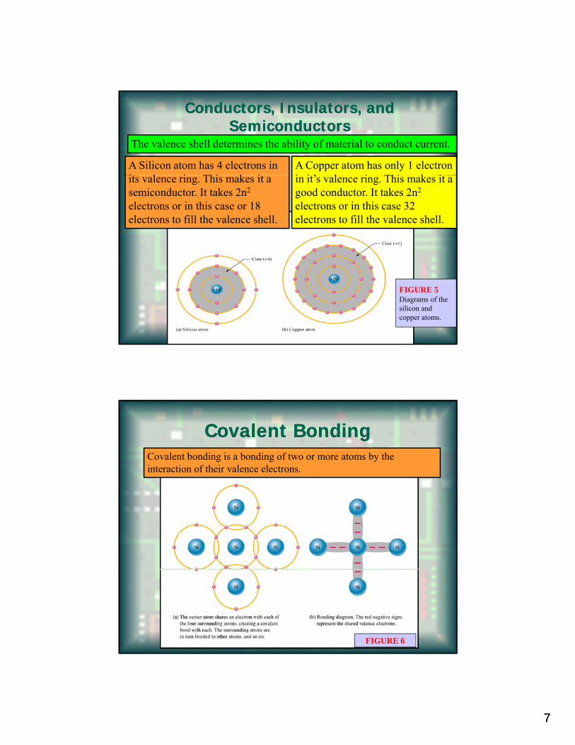
Conductors, Insulators, and Conductors, Insulators, and SemiconductorsSemiconductors
The ability of a material to conduct current is based on its atomic structure.based on its atomic structure.
The orbit paths of the electrons surrounding the nucleus are called shells.
Each shell has a defined number of electrons it will hold. This is a fact of nature and can be determined by the formula N = 2n2
The less complete a shell is filled to capacity the more conductive the material is.
determined by the formula, Ne = 2n .
The outer shell is called the valence shell.

55
• All elements are arranged in the periodic table of the
Atomic numberAtomic number, , Electron shells & OrbitsElectron shells & Orbits, , Valence electrons, and IonizationValence electrons, and Ionization
g pelements in order according to their atomic number.The atomic number equals the number of protons in the nucleus, which is the same as the number electrons.
• Electron shells and Orbits• The outmost shell is known as the Valence shell andThe outmost shell is known as the Valence shell and
electrons in this shell are called valence electrons.• The process of losing a valence electron is known as
ionization (i.e. positive ion and negative ion).
Electron shells and OrbitsElectron shells and Orbits
FIGURE 3 Energy levels increase as the distance from the nucleus increases.

66
Conductors, Insulators, Conductors, Insulators, and Semiconductorsand Semiconductors
• A conductor is a material that easily conducts electrical current. The best conductors are single-element material,
h ld d l i hi hsuch as copper, gold, and aluminum, which are characterized by atoms with only one valence electron very loosely bound to the atom.
• An insulator is a material that does not conduct electrical current under normal conditions. Valence electrons are tightly bound to the atoms.g y
• A semiconductor is a material that is between conductors and insulators in its ability to conduct electrical current. The most common single –element semiconductors are silicon, germanium, and carbon.
Energy BandsEnergy Bands
FIGURE 4 Energy band diagram for a pure (intrinsic) silicon crystal with unexcited atoms. There are no electrons in the conduction band.
77
The valence shell determines the ability of material to conduct current.
A Copper atom has only 1 electron i i ’ l i Thi k i
A Silicon atom has 4 electrons in i l i Thi k i
Conductors, Insulators, and Conductors, Insulators, and SemiconductorsSemiconductors
in it’s valence ring. This makes it a good conductor. It takes 2n2
electrons or in this case 32 electrons to fill the valence shell.
its valence ring. This makes it a semiconductor. It takes 2n2
electrons or in this case or 18 electrons to fill the valence shell.
FIGURE 5Diagrams of the silicon and copper atoms.
Covalent BondingCovalent BondingCovalent bonding is a bonding of two or more atoms by the interaction of their valence electrons.
FIGURE 6

88
Silicon and GermaniumSilicon and Germanium
FIGURE 7 Diagrams of the silicon and germanium atoms.
Conduction in SemiconductorsConduction in Semiconductors
FIGURE 9 Energy band diagram for a pure (intrinsic) silicon crystal with unexcited atoms. There are no electrons in the conduction band.

99
DopingDoping
The controlled addition of impurities (Pentavalent The controlled addition of impurities (Pentavalent or Trivalent) to the intrinsic (pure) Si or Ge or Trivalent) to the intrinsic (pure) Si or Ge drastically increased the conductivity and make drastically increased the conductivity and make them useful in electronic devices. This process of them useful in electronic devices. This process of addition of impurity is known as doping and the addition of impurity is known as doping and the two categories of impurities are called ntwo categories of impurities are called n--type and type and pp--type.type.
NN--type and Ptype and P--type Semiconductorstype SemiconductorsOther atoms with 5 electrons(pentavalent atom) such as A ti dd d t Sili
Other atoms with 3 electrons(trivalent atoms) such as Boron are dd d t Sili t t d fi iAntimony are added to Silicon
to increase the free electrons.
N-type
added to Silicon to create a deficiency of electrons or hole charges.
P-type

1010
The Depletion RegionThe Depletion RegionP-region N-region P-region N-region
Every electron that diffuse across the pn-junction combines with a hole in p region and left behind a positive charge (hole) in n region Thisin p-region and left behind a positive charge (hole) in n-region. This results a negative charge in p-region, forming a barrier potential at pn-junction. This action continues until the voltage of the barrier repels further diffusion. These two layers of positive and negative charge is called Depletion Region. Barrier potential cannot be measured with a voltmeter but it will cause a small voltage drop during conduction.
Introduction to DiodeIntroduction to Diode(PN Junction)(PN Junction)
• If a block of Si is doped with p-type and n-type impurities, i ll d th j ti i f d t th b da region called the pn-junction is formed at the boundary
between the two, and a diode is formed.
• It is a simplest semiconductor device with symbol:
• It is a two terminal device.

1111
Basic Operation of DiodeBasic Operation of DiodeIdeally it Ideally it conducts current inconducts current in only one directiononly one direction
and acts like an and acts like an open in the opposite direction.open in the opposite direction.
Biasing the Diode : Biasing the Diode : Forward BiasForward Bias
• When a DC voltage is applied across a diode, it is called Biasing. • If the application of DC voltage creates a condition that allows diode to
conduct current, it is called Forward Bias. In forward biasing positiveconduct current, it is called Forward Bias. In forward biasing positive terminal of biasing voltage (VBIAS) is connected to p-region and negative terminal is connected to n-region.
• In Figure, resister R limits the current to avoid any unwanted situation -damage to diode.
• As a Result of Forward Bias, the depletion region is decreased and a drop across the pn-junction is produced equal to the barrier potential (0.7V).

1212
Forward Bias Forward Bias (Continued)(Continued)
FIGURE 10 A forward-biased diode showing the flow of majority carriers and the voltage due to the barrier potential across the depletion region.
Biasing the Diode : Biasing the Diode : Reverse BiasReverse Bias
• Voltage source or bias connections are ve to the p region and• Voltage source or bias connections are – ve to the p-region and + ve to the n-region.
• Bias must be less than the break down voltage.
• Current flow is negligible in most cases.
• The depletion region widens.

1313
Reverse Bias Reverse Bias (Continued)(Continued)
FIGURE 11 The diode during the short transition time immediately after reverse-bias voltage is applied.
Forward Bias Measurements With Forward Bias Measurements With Small Voltage AppliedSmall Voltage Applied
In this case with the voltage applied is less than the barrier potential (the diode for all practical purposes) i till iis still in a non-conducting state. Current is very small.

1414
Forward Bias Measurements With Forward Bias Measurements With Applied Voltage Greater Than the Barrier VoltageApplied Voltage Greater Than the Barrier Voltage
With the applied ppvoltage exceeding the barrier potential (for fully forward biased), the diode conducts. Note that h l i lthe only practical
loss is the .7 Volts dropped across the diode.
Connection Diagrams Connection Diagrams
Forward-bias and reverse-bias connections showing the diode symbol.

1515
The Ideal Diode ModelThe Ideal Diode Model
VF = 0 V
BIASF R
VI =
In this characteristic curve we do not consider the voltage drop or the resistive
ti C t LIMITR
IR = 0 AVR = VBIAS
properties. Current flow proportionally increases with voltage.
The Practical Diode ModelThe Practical Diode Model
VF = 0.7 V (silicon)VF = 0.3 V (germanium)
LIMITRVFVBIASV =−− 0
In most cases we consider only the forward bias voltage drop of a diode. Once this voltage is
LIMITRFILIMITRV =
LIMITR
FVBIASV
FI−
=
this voltage is overcome the current increases proportionally with voltage.This drop is particularly important to consider in low voltage applications.

1616
The Complete Diode ModelThe Complete Diode Model
'7.0 drFIFV += '
7.0
drLIMITR
BIASV
FI+
−=
VV--I Characteristic for I Characteristic for Forward BiasForward Bias
(a) V-I characteristic curve for forward bias. Part (b) illustrates how the dynamic resistance r’d decreases as you move up the curve (r’d = ∆VF/∆IF).

1717
VV--I Characteristic for I Characteristic for Reverse BiasReverse Bias
V-I characteristic curve for reverse-biased diode.
CompleteComplete VV--I Characteristic CurveI Characteristic Curve

1818
Actual Diode CharacteristicsActual Diode Characteristics
Note the regions for No Bias, Reverse Bias, and Forward Bias conditions.Note the regions for No Bias, Reverse Bias, and Forward Bias conditions.Look closely at the scale for each of these conditions!Look closely at the scale for each of these conditions!
35353535
NumericalNumerical

1919
Troubleshooting DiodesTroubleshooting DiodesTesting a diode is quite simple, particularly if the multimeter used has a diode check function. With the diode check function from the meter a specific known voltage is applied across the diode.p g pp
With the diode check function a good diode will show approximately .7V (Si) or .3V (Ge) when forward biased.
When checking in reverse bias the full applied testing voltage will be seen on the display.
Troubleshooting DiodesTroubleshooting DiodesOpen Diode
In the case of an open diode no current flows in either direction which is indicated by the full checking voltage with the diode check function or high resistance using an ohmmeter in both forward and reverse connections.
Shorted DiodeIn the case of a shorted diode maximum current flows indicated by a 0 V with the diode check function or low resistance with an ohmmeter in both forward and reverse connections.

2020
Sajid Ansari , P.Eng. PMP.A. Professor (UIT).A. Professor (UIT).