1 lcos spatial light modulators: trends and applications
TRANSCRIPT

1
1LCOS Spatial Light Modulators: Trends and ApplicationsGrigory Lazarev, Andreas Hermerschmidt, Sven Kruger, and Stefan Osten
1.1Introduction
Spatial light modulator (SLM) is a general term describing devices that are usedto modulate amplitude, phase, or polarization of light waves in space and time.Current SLM–based systems use either optical MEMS (microelectromechanicalsystem, [1]) or LCD technology [2]. In this chapter, we review trends and applicationsof SLMs with focus on liquid crystal on silicon (LCOS) technology.
Most developments of liquid crystal (LC) microdisplays are driven by consumerelectronics industry for rear–projection TVs, front projectors, and picoprojectors.Also, MEMS technologies such as digital micromirror device (DMD, [3]) and gratinglight valve (GLV, [4]) are driven by these industries, except for membrane mir-rors. Some industrial applications have forced MEMS development for scanning,printing technologies, and automotive applications [5]. But the major R&D-relateddriving force for new SLM technologies is the defense industry.
Technological advances in lithography are the basis for MEMS developments.Phase modulators based on 2D pistonlike mirror arrays [6, 7] or ribbonlike 1Dgratings [8] show high performance in frame rate. Unfortunately, the availability ofthese technologies is limited because they are developed either company-internalor within defence projects. The major advantages of MEMS are frame rate, spectralrange, and an efficient use of nonpolarized light. Phase modulators and otheroptical implementations are still niche markets for the MEMS industry. Even now,customized MEMS developments are quite challenging and expensive.
LC panels still have an advantage out of their projection applications in termsof resolution and minimal pixel size for 2D displays. Only LC-based technologyis able to modulate intensity, phase, and/or polarization because of polarizationrotation and/or electrically controlled birefringence (ECB).
LCOS technology [9] was developed for front- and rear- (RPTV) projectionsystems competing with AMLCD (active matrix LCD) and DMD. The reflectivearrangement due to silicon backplane allows putting a high number of pixelsin a small panel, keeping the fill factor ratio high even for micrometer-sizedpixels.
Optical Imaging and Metrology: Advanced Technologies, First Edition.Edited by Wolfgang Osten and Nadya Reingand.© 2012 Wiley-VCH Verlag GmbH & Co. KGaA. Published 2012 by Wiley-VCH Verlag GmbH & Co. KGaA.

2 1 LCOS Spatial Light Modulators: Trends and Applications
The history of companies shutting down their LCOS activities (Intel, Philips,etc.) and the downfall of the RPTV market made it difficult to demonstrate thepromised LCOS advantages in performance and volume pricing. However, theclassic three-panel architectures for high-end front- and rear-projection systems ledto the development of high-quality microdisplays, high-performance polarization,and compensation optics as well as sophisticated electronic driving solutions.Single-panel designs for field sequential color systems never really entered thehigh-end and professional market, but are as good candidates as DMD and laserscanning technologies for small and embedded projection devices, such as cellphone, companion, camera, and toy projectors.
1.2LCOS-Based SLMs
LCOS SLMs based on ‘‘consumer’’ microdisplay technology inherited features anddrawbacks of projection displays. Backplanes of the front-projection microdisplaysusually have a diagonal exceeding 0.55 in. or higher and pixel sizes startingfrom 8 μm. Smaller panels are not popular in front-projection microdisplaysbecause of etendue limitations when used in an incoherent system [10] as well asheat dissipation considerations. However, microdisplays intended for embeddedprojectors and picoprojectors utilize quite small panels from 0.17 to 0.55 in. withpixel sizes ranging from 6 to 10 μm. Whereas HMD products require a larger paneldiagonal for high field of view (FOV) designs. Reduction of the pixel size has asignificant economical advantage in customer electronics industry since it allowsplacing more dies on the wafer. Both types of microdisplays are usually drivencolor field sequential, which means they offer a higher frame rate when potentiallyused as SLMs.
1.2.1LCOS Technology
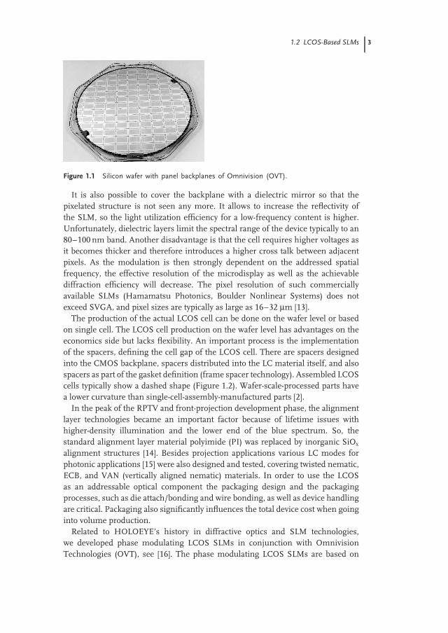
1.2.1.1 Manufacturing and Assembly TechnologiesLCOS technology has different descriptions/brand names with different suppliers;for example, JVC’s ‘‘D-ILA’’ and Sony’s ‘‘SXRD,’’ are basically the same CMOSwafer technology, processed typically using 8 in. silicon wafers (Figure 1.1). BothSony and JVC introduced 4K LCOS panels (4096 × 2160 and 4096 × 2400) to themarket. JVC was also successful in building a prototype of an 8K panel (8192 ×4320) with 5 μm pixel size [11].
In order to get a good reflectivity out of these reflective pixelated arrays, highreflective aluminum mirrors, mostly with a passivation layer, are used. Varioustechniques for planarization or reduced interpixel gap effects have been developedover the years. At present, foundries offer processes to reduce the interpixel gap inthe design down to 200 nm [12].
1.2 LCOS-Based SLMs 3
Figure 1.1 Silicon wafer with panel backplanes of Omnivision (OVT).
It is also possible to cover the backplane with a dielectric mirror so that thepixelated structure is not seen any more. It allows to increase the reflectivity ofthe SLM, so the light utilization efficiency for a low-frequency content is higher.Unfortunately, dielectric layers limit the spectral range of the device typically to an80–100 nm band. Another disadvantage is that the cell requires higher voltages asit becomes thicker and therefore introduces a higher cross talk between adjacentpixels. As the modulation is then strongly dependent on the addressed spatialfrequency, the effective resolution of the microdisplay as well as the achievablediffraction efficiency will decrease. The pixel resolution of such commerciallyavailable SLMs (Hamamatsu Photonics, Boulder Nonlinear Systems) does notexceed SVGA, and pixel sizes are typically as large as 16–32 μm [13].
The production of the actual LCOS cell can be done on the wafer level or basedon single cell. The LCOS cell production on the wafer level has advantages on theeconomics side but lacks flexibility. An important process is the implementationof the spacers, defining the cell gap of the LCOS cell. There are spacers designedinto the CMOS backplane, spacers distributed into the LC material itself, and alsospacers as part of the gasket definition (frame spacer technology). Assembled LCOScells typically show a dashed shape (Figure 1.2). Wafer-scale-processed parts havea lower curvature than single-cell-assembly-manufactured parts [2].
In the peak of the RPTV and front-projection development phase, the alignmentlayer technologies became an important factor because of lifetime issues withhigher-density illumination and the lower end of the blue spectrum. So, thestandard alignment layer material polyimide (PI) was replaced by inorganic SiOx
alignment structures [14]. Besides projection applications various LC modes forphotonic applications [15] were also designed and tested, covering twisted nematic,ECB, and VAN (vertically aligned nematic) materials. In order to use the LCOSas an addressable optical component the packaging design and the packagingprocesses, such as die attach/bonding and wire bonding, as well as device handlingare critical. Packaging also significantly influences the total device cost when goinginto volume production.
Related to HOLOEYE’s history in diffractive optics and SLM technologies,we developed phase modulating LCOS SLMs in conjunction with OmnivisionTechnologies (OVT), see [16]. The phase modulating LCOS SLMs are based on

4 1 LCOS Spatial Light Modulators: Trends and Applications
−1.0
−0.4
0.3
0.9
2.2
1.6
−1.0
−0.4
0.3
0.9
2.2
1.6
Sur
face
dev
iatio
n / μ
m
PV: 3.0RMS: 0.6μm
Points: 44902
1513
1210
87
53
20 0
123
455678
y axis (mm)
x ax
is (m
m)
Meas. wavelength = 633 nm
Figure 1.2 Curvature of the microdisplay measured with a Twyman–Green interferometer.
OVT’s commercially available 0.7 in. full HD backplane and have been used innumerous adaptive optics applications. HOLOEYE is using nematic LC for theirLCOS SLMs with almost analogous phase modulation, because of the higherdiffraction efficiency of multilevel hologram structures (256 level, typically 80%).This is one of the main advantages compared with ferroelectric LC (FLC) technology,as FLC can only display binary holograms that always create a symmetrical imageleading to a basic 50% loss of light in the system in addition to 50% duty cycleof FLCs. The clear advantage of the FLC is its switching speed, that is,it can berefreshed in the kilohertz range.
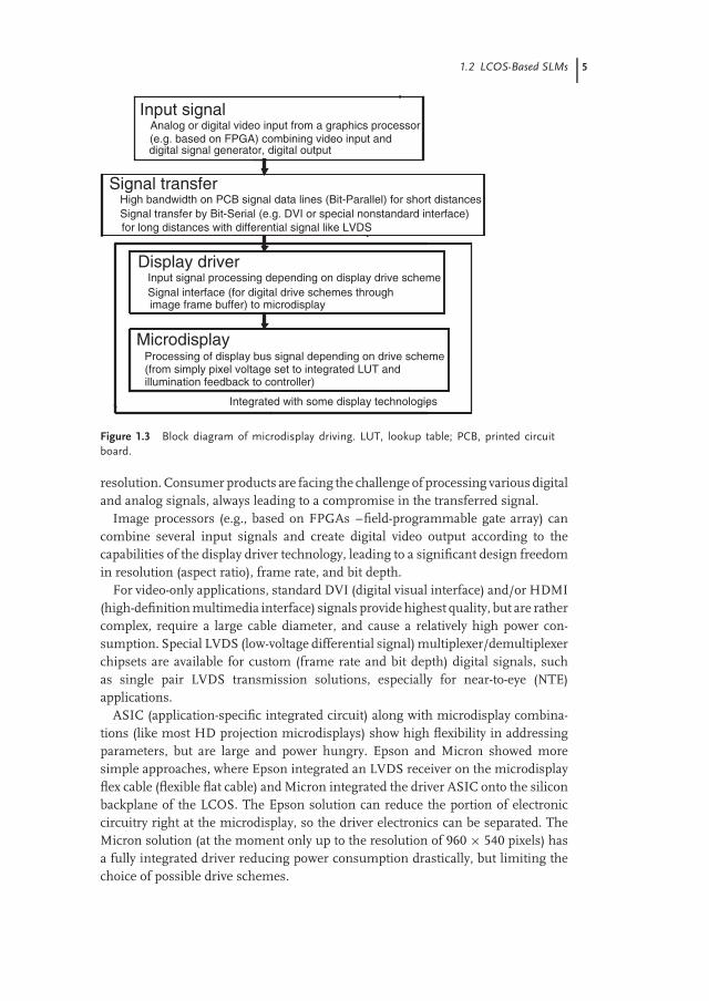
1.2.1.2 Signal FlowIn most microdisplay technologies/applications, the signal flow starts with a definedinput signal form to be transferred to the microdisplay driver directly in contactwith the microdisplay. The schematic representation shown in Figure 1.3 can beused to derive the first batch of parameters leading to an optimized microdisplaydrive solution.
Most pixel-based display technologies show a native resolution of a certain displaystandard (compare, e.g., VESA (Video Electronics Standards Association)), showingoptimized performance with input signals representing this native resolution. Forhigher quality microdisplays, the device can embed the input signal of lowerresolution into the physical pixel matrix, filling the whole array of pixels. Puredigital input signals and an EDID (extended display identification data) adapted tothe display controllers guarantee the correct choice of timing and addressed display
1.2 LCOS-Based SLMs 5
Analog or digital video input from a graphics processor(e.g. based on FPGA) combining video input and digital signal generator, digital output
High bandwidth on PCB signal data lines (Bit-Parallel) for short distancesSignal transfer by Bit-Serial (e.g. DVI or special nonstandard interface)for long distances with differential signal like LVDS
Input signal processing depending on display drive schemeSignal interface (for digital drive schemes throughimage frame buffer) to microdisplay
Processing of display bus signal depending on drive scheme(from simply pixel voltage set to integrated LUT andillumination feedback to controller)
Integrated with some display technologies
Figure 1.3 Block diagram of microdisplay driving. LUT, lookup table; PCB, printed circuitboard.
resolution. Consumer products are facing the challenge of processing various digitaland analog signals, always leading to a compromise in the transferred signal.
Image processors (e.g., based on FPGAs –field-programmable gate array) cancombine several input signals and create digital video output according to thecapabilities of the display driver technology, leading to a significant design freedomin resolution (aspect ratio), frame rate, and bit depth.
For video-only applications, standard DVI (digital visual interface) and/or HDMI(high-definition multimedia interface) signals provide highest quality, but are rathercomplex, require a large cable diameter, and cause a relatively high power con-sumption. Special LVDS (low-voltage differential signal) multiplexer/demultiplexerchipsets are available for custom (frame rate and bit depth) digital signals, suchas single pair LVDS transmission solutions, especially for near-to-eye (NTE)applications.
ASIC (application-specific integrated circuit) along with microdisplay combina-tions (like most HD projection microdisplays) show high flexibility in addressingparameters, but are large and power hungry. Epson and Micron showed moresimple approaches, where Epson integrated an LVDS receiver on the microdisplayflex cable (flexible flat cable) and Micron integrated the driver ASIC onto the siliconbackplane of the LCOS. The Epson solution can reduce the portion of electroniccircuitry right at the microdisplay, so the driver electronics can be separated. TheMicron solution (at the moment only up to the resolution of 960 × 540 pixels) hasa fully integrated driver reducing power consumption drastically, but limiting thechoice of possible drive schemes.

6 1 LCOS Spatial Light Modulators: Trends and Applications
1.2.1.3 Drive Schemes and LatencyTwo major types of drive schemes are used: analog and digital, and this differenti-ation is based on the actual generated voltage applied to individual pixels.
Analog Drive In analog drive schemes, the microdisplay utilizes analog voltagesdirectly for the representation of a gray level in an individual LC cell. The schemeis well suited for short illumination pulses because of analog voltages on the pixel(there is no specific digital flicker noise, see further). Analog drive uses typicallylower clock frequency and hence has lower power consumption. As a result, longerflex cables between driver and microdisplay are possible.
The analogue scheme also has a number of drawbacks. Drift- andchannel-depending variations of drive voltages need to be compensated. The abilityfor that compensation is evidently limited. The display addressing is progressive,that is, pixels are addressed in a consecutive way and not simultaneously.Effectively, the video signal goes through a low-pass filter. The analog signal pathaffects the slew rate of the video signal and can superimpose ringing, nonlineardistortion, noise, and echoes. Since the frequency of the video signal is relativelylow in the vertical direction and relatively high in the horizontal direction, asignificant ‘‘cross talk’’ occurs for the latter one, that is, for sequentially writtenpixels. As a result, a decrease of phase (or amplitude) modulation for high spatialfrequencies in the addressed image is observed [17], which corresponds to adecrease in resolution.
The field inversion, which is always required in LCs, in typical analog progressivescan architectures is limited to the single or double frame rate. In the case of thesingle frame rate field inversion, the DC balancing can fail if the content changestoo fast (e.g., due to a specific application). This can cause lifetime issues, that is,destroy the transparent electrode (Indium tin oxide (ITO)). The inversion with thedouble frame rate requires a frame buffer [18].
Digital Fast Bit-Plane Addressing In a digital drive scheme a pulse width modula-tion (PWM) encodes a certain gray level into a series of binary pulses in the kilohertzrange, referred to as sequence. In principle, every individual pulse interacts withthe LC molecule, causing its rotation, that at the end leads to the desired graylevel representation. Owing to limited rotational viscosity of the LC material, LCmolecules cannot follow individual pulses of the electrical signal in a discrete way.That is why the base addressing frequency cannot be resolved, so that it is possibleto achieve an almost analogous LC molecule position representing/resulting in acertain gray level.
The digital scheme is usually more stable than analog and shows a repeatableperformance. Field inversion is possible at the kilohertz range (e.g., for each mod-ulation pulse) without image retention. All pixels are addressed simultaneously.The scheme does not suffer from electrical cross talk (i.e., no low path filteringof the signal). However, an electro-optical cross talk for small pixel sizes may stillbe observable. The electro-optical cross talk is caused by influence of the electricalfield between adjacent pixels and can be further compensated [19].

1.2 LCOS-Based SLMs 7
The control electronics of such microdisplays is compact and has low cost.The device itself is highly programmable. The addressed resolution, amplitude orphase bit depth, and frame rate can be changed in situ and if required, adapted toenvironmental changes (e.g., wavelength, temperature).
The advantages of digital addressing are accompanied by limitations. Oneobserves a kind of flicker noise at high frequencies (‘‘supermodulation’’). Thismeans the electro-optical response of the SLM is not constant over the frame. Insome scenarios (e.g., projection) time averaging can be used to compensate thiseffect. In other scenarios, in particular, when using phase modulation or short-pulselight sources, time averaging is not possible. Here, special sequences and higherbandwidth to the LCOS panel help to reduce the flicker noise to acceptable level.Another option is synchronization between the light source and the SLM at theframe rate.
OVT Display Driving The OVT technology, implemented in HOLOEYE’s phaseSLMs, uses a digital PWM technique, based on the idea, that a fast sequence ofbinary modulation can realize an almost analogous response, in particular, for alow bandwidth detector, for example, the human eye. In this way, LC microdisplayswith binary modulating FLC material and MEMS technologies, such as digital lightprocessing (DLP), are operated to deliver gray scale modulation. With nematic LCtechnology, we also have to consider the larger response time of this LC materialleading to an almost analogous optical response because of the convolution ofthe digital pulse code and the LC response time. With OVT’s technology [20], it isactually not the ‘‘pulse width’’ that is varied, whereas the gray scale encoding is doneby the sequence of bits. The bits of the sequence have individual durations, selectedfrom the set of fixed values. This pulse code modulation (PCM) is advantageousbecause of the bandwidth limitation and the digital nature of the drive concept.A typical PCM sequence consists of bits with different weights (duration), whichare independently programmable, which is repeated every video frame. With thisapproach, the sequence design offers a lot of flexibility, enabling the microdisplayto be driven with different frame rates, color bit depth, and color frames. Here, asimple 10 bit interface could be used for RGB (sequentially reproduced red, green,and blue) 3 : 4 : 3 bit depth system, which for technical applications shows a quitereasonable performance. For color systems with mainly monochromatic content(e.g., green) a 2 :6 : 2 bit depth can also be designed and programed.
The effective latency not only depends on the LC response time but also on thedrive scheme. The analog drive is typically operated in an ‘‘unbuffered’’ mode,where the pixel data can be directly addressed to the microdisplay. The analog driveuses a progressive scan approach, where there is a continuous serial refresh of thepixel information.
However, the fast bit-plane addressing needs memory for storing the imagecontent. With the incoming video information, the pulse sequence (encoding thegray value) for the individual pixel is written into a frame buffer. With the nextframe, binary information for all pixels (the so-called bit planes) is transferred to

8 1 LCOS Spatial Light Modulators: Trends and Applications
all pixels at the same time. The individual gray values are realized with a sufficientnumber of bit planes.
Most digital drive schemes are designed for video applications, where the humaneye is the detector. Any supermodulation (flicker) above 100Hz is almost notnoticeable. For applications using a pulsed light source, such as light-emittingdiode (LED) or laser, the PWM of the digital display drive could interfere with thelight source driving as it was already mentioned above. It is worth mentioning thatthe electronic addressing bandwidth is the key in defining the right addressingfrequency.
1.2.2Operation Modes
The use of LC materials in SLMs is based on their optical and electrical anisotropy.Typically, a thin layer of LC material can be described as a birefringent materialwith two refractive indices. The orientation of the index ellipsoid is dependent onthe direction of the molecular axis. This orientation is determined by the alignmentlayers of the LC cell. The most important cases are twisted, parallel aligned (PA),and vertical aligned (VA) cells. In a twisted cell, the orientation of the moleculesdiffers by typically 90◦ between the top and the bottom of the LC cell and is arrangedin a helix-like structure in between. In both PA and VA cells, the alignment layersare parallel to each other, so the LC molecules have the same orientation.
The effect of an LC cell on a monochromatic, polarized light wave can bedescribed by a Jones matrix. Here, ‘‘polarized’’ does not necessarily refer to linearpolarization, but to a fully polarized state in the sense that the Stokes parameters[21] add up to 1. For PA and VA cells, the Jones matrix [22] is given by
WPN−LC = exp(−iφ)(
exp(−iβ) 00 exp(iβ)
)(1.1)
where the birefringence β and the phase offset φ are given by
β = (neo − no)πd
λ(1.2a)
φ = (neo + no)πd
λ(1.2b)
where no and ne are the ordinary and extraordinary indices of refraction of theLC material, respectively, d is the thickness of the cell, and λ is the wavelength ofthe light field. The possibility of changing the birefringence β as a function of thevoltage applied to the LC cell makes this component a switchable waveplate.
The Jones matrix of a TN-LC cell is dependent on the physical parameters twistangle, α, front director orientation, ψ , and birefringence, β. It is given by [23]
WTN−LC(f , h, g, j) = exp −iφ
(f − i · g h − i · j−h − i · j f + i · g
)(1.3)

1.2 LCOS-Based SLMs 9
using parameters f , g, h and j which fulfill f 2 + g2 + h2 + j2 = 1 and can becalculated from the physical cell parameters as
f = cos γ cos α + α
γsin γ sin α (1.4a)
h = cos γ sin α − α
γsin γ cos α (1.4b)
g = β
γsin γ cos(2ψ − α) (1.4c)
j = β
γsin γ sin(2ψ − α) (1.4d)
where the parameter γ is given by
γ =√
α2 + β2 (1.5)
The phase factor exp(−iφ) can be neglected for most applications. For somecommercially available TN-LC-cell-based microdisplays, the parameters α, β, andψ were not made available by the manufacturers but could be retrieved from opticalmeasurements [24].
It is obvious that the first case of a PA or VA cell is more convenient, at least ifwe are interested in creating pure phase modulation or polarization modulation.
1.2.2.1 Amplitude ModulationThis modulation type can be achieved with twisted, PA, as well as VA LC cells in asimple optical configuration. The incident light field should be linearly polarized,and after passing through the LC cell, it should be transmitted through a polarizeroriented perpendicular to the incident polarization. For an LCOS-SLM, a polarizingbeam-splitter cube is suitable to obtain this. For PA or VA cells, the orientation ofthe optical axis should be rotated by 45◦ with respect to the incident polarization.For a phase delay of π introduced by the cell, the polarization appears to be rotatedby 90◦. The level of attenuation by the second polarizer can be tuned by applyingan electric field to the cell, which leads to a change of the birefringence β.
This regime is normally used by projection displays. The three-panel architecturein front projectors can realize very high contrast ratio values above 70 000:1 (JVCDLA-RS series). To get the panels toward fast response time, the VAN mode is used,in which the LC material has a considerable pretilt (also in order to avoid reversedomains), which leads to a residual retardation effect in the dark state, and thisneeds to be compensated to achieve high contrast ratio. A variety of compensationtechnologies are available [25, 26], whereas these days, the preferred componentsare quarter-wave plates (QWPs) and specific retarder plates (see e.g., [22]).
1.2.2.2 Phase ModulationWe have seen that a PA LC cell can be interpreted as a switchable waveplate(Eqs. (1.1) and (1.2a)). It is evident that on transmission through a PA LC cell, lightpolarized linearly parallel to the extraordinary axis of the LC material is retardedas a function of the voltage-controlled birefringence β (this mode is also known

10 1 LCOS Spatial Light Modulators: Trends and Applications
as ECB). Therefore, such cell is a convenient phase-only modulator for linearlypolarized light.
Obtaining phase-only modulation using twisted cells is significantly more com-plicated. It has been shown that there are elliptic polarization states that are onlysubject to phase modulation, with tolerable amplitude modulation introduced bya polarizer behind the SLM [27, 28]. This mode of operation is often referred toas phase-mostly operation. Creating the appropriate elliptic polarization requires aQWP, as well as the conversion to a linearly polarized state behind the SLM.
This regime has many applications ranging from wavefront control (with typi-cally slowly varying phase functions) to dynamic computer-generated holography(with typically fast spatial variation of the phase function). In the latter case, asuitable algorithm for the creation of the phase-only hologram is required. Suchcomputational algorithms have been adapted to match the particular needs of SLMapplications in order to deal with fringe field effects, [29], optimize the speed ofholographic computations [30], obtain a free choice of diffraction angles [31], andreduce the intensity fluctuations during frame-to-frame SLM update [32].
1.2.2.3 Polarization ModulationWhen placing a waveplate of variable retardance (‘‘WP1’’) between two QWPs,with the optical axes of these QWPs rotated by +45◦ and −45◦ with respect to theoptical axis of WP1, the Jones matrix of the three waveplates together is a rotationmatrix in which the rotation angle is given by the phase shift of WP1. Therefore itis possible to convert a phase modulating SLM into a 2D matrix of phase-rotatingpixels by sandwiching it between two such QWPs. Interestingly, the polarizationrotating feature is not dependent on the polarization of the incident light wave,only on the degree of polarization, which should be 1, and its wavelength. To givean example, this means that by addressing a vortex phase function to the SLM,a linearly polarized beam can be converted into a beam with radial or azimuthalpolarization.
1.2.2.4 Complex-Valued ModulationA desired mode of operation would be the ability to change both amplitude andphase of an incoming wavefront simultaneously, thereby creating a complex-valuedtransmittance of the SLM. From the discussion above it is evident that while ofcourse phase and amplitude can be modulated by a single cell, the amplitudeand phase values cannot be chosen independently, which makes complex-valuedoperation using a single cell almost unusable. Following are the options to representa complex-valued transmittance by using special configurations.
• Stacking two LC cells: This involves sandwiching two LC layers and operatingone in phase-only and the the other in amplitude-only mode. A transmissiveSLM with a 1D array of pixels is manufactured by Cambridge Research andInstrumentation, but for 2D arrays of pixels the control of the two independentvoltages required for each pixel has prevented the realization of such device.
• 4f imaging: In this option two SLM devices, including polarizer(s), with twolenses in 4f configuration are used and one device is operated in phase-only
1.2 LCOS-Based SLMs 11
and the other in amplitude-only mode (or vice versa),. Apart from the spatialfrequency bandwidth limitation and inevitable optical aberrations, this would bethe straightforward equivalent to physically stacking two LC cells.
• Macro pixel technique: In this, two adjacent pixels can be used to representthe real and imaginary parts of the desired complex transmittance [33] or canbe combined together with help of additional thin components, which providesbetter quality of reconstruction in digital holography [34]; three amplitude pixelscan very well represent a complex value [35], and using four pixels, it is possibleeven to use TN cells with mixed polarization and phase modulation [36].
• Spatial multiplexing: In the special case that the desired complex distributionis the sum of two phase functions it is an option to use a single phase-onlySLM and to display each phase function in only every second of the availablepixels. The pixel locations used for each phase function can simply be a randompattern [37].
1.2.3Performance Evaluation
The evaluation of the SLM performance for digital holography applications typicallycomprises evaluation of phase response versus addressed value (linearity andmaximal achievable phase delay) as well as phase response versus time, crosstalkversus spatial frequencies, flatness of the display, response times, and crossmodulation.
Phase response can be measured using a Michelson interferometer or also witha common path interferometer [38]. Alternatively, it is possible to get a goodestimation indirectly, using amplitude modulation mode. In this case, the incidentpolarization is oriented at 45◦ to the slow axis (in phase mode, it is parallel) and theanalyzer is set perpendicular to the incident polarization. However, the advantageof a Michelson interferometer is that it is well suited for determining the flatnessof the SLM at the same time (Figure 1.2).
Measurement of the phase response requires a high-speed detector, becausethe specific digital noise has relatively high frequency. One indirect method is toaddress diffraction gratings to the SLM and to observe intensity of the diffractionorders with a single detector (photodiode), attached to an oscilloscope. This methodactually measures the diffraction efficiency over time. Another indirect method isto use an amplitude modulation mode, that is, to measure intensity noise overtime. A more direct measurement can be performed using an interferometer withfast acquisition or with a stroboscopic technique [39].
Cross talk can be well evaluated with a simple approach, in which diffractionefficiency is measured versus addressed phase value for different spatial frequen-cies. The resulting curves can be used to derive actual phase modulation of theaddressed grating versus addressed values [38].
Cross modulation is a residual amplitude modulation, which accompanies phasemodulation. Residual amplitude modulation means that light coming from theSLM has a certain ellipticity in polarization state. This is simple to measure using

12 1 LCOS Spatial Light Modulators: Trends and Applications
an analyzer, which is oriented parallel to the incident polarization, and a powermeter. More generally, as mentioned above, a full Jones matrix can be determinedand taken into account later in the calculation of holograms [40, 41]. Responsetimes can be basically evaluated with an oscilloscope and photodiode, observingdiffraction order intensity of an addressed grating (the grating is then switched onand off). Alternatively, measurements in amplitude modulation mode as well astime-resolved phase measurements can be considered (as already mentioned).
Also of importance is the quality of anti-reflection (AR) coating of the front andback surfaces of the cover glass. Parasite reflections created by one of this surfacescan cause Fabry-Perot-type interferences in the microdisplay.
For industrial and high-power applications, the behavior of SLM in responseto temperature can be important. It is defined mainly by the dependence of theviscosity of the LC material on temperature. Higher temperatures usually decreaseresponse times and increase phase modulation values at the cost of increasingtemporal noise.
1.3Some Applications of Spatial Light Modulators in Optical Imaging and Metrology
SLMs are used in a wide variety of applications mostly as a phase modulator,among which are measurement systems, microscopy, telecommunications, anddigital holography. Meeser et al. [42] developed a holographic sensor, using an SLMto adapt the reference wave for different object positions as well as a flexible phaseshifter. The SLM allows to switch between Fresnel and Fourier holograms and todetermine accurately the phase distribution in the CCD plane using phase shiftingalgorithms (Figures 1.4 and 1.5). Another system from the same group works using
Spherical
CCD
PPBSQWPP
SLM
Object
referencewave
Figure 1.4 Schematic layout of the holographic sensor. P, polarizer; QWP, quarter-waveplate; PBS, polarizing beam splitter; CCD, detector. (Source: Adapted with permission from[42].)

1.3 Some Applications of Spatial Light Modulators in Optical Imaging and Metrology 13
Figure 1.5 Numerical reconstruction of the hologram, captured with the holographicsensor. Source: With permission from [42].
the shearography principle, where the SLM performs the function of a shear [43],see also Chapter 17. Schaal et al. [44] proposed to use a phase SLM in a multipointdynamic vibrometer, where the vibration is simultaneously measured in a freelyselectable set of points. Baumbach et al. [45] demonstrated a digital holographytechnique, which replaces the holographic interferometry and implements SLMfor achieving ‘‘analog’’ optical reconstruction of the master object.
Jenness [46] demonstrated the use of a phase SLM in a holographic lithographysystem (Figure 1.6), in which he successfully processed micropyramid structures(Figure 1.7) in photoresist [47, 48]. The main limitation of lithography applicationswith LCOS is the UV absorption of the LC cell, which does not allow the use of shortwavelengths and hence affects the increase of the resolution of the lithography.Even though there exist transmission windows in the absorption spectrum [49,50], the use of these windows does not look feasible. More flexible might be acombination of holographic lithography with two-photon lithography [51], whichgives the possibility of working in the visible spectrum and then halving thewavelength due to the two-photon effect in the object plane. A similar principle wasused in the realization of scanless two-photon microscopy by Nikolenko et al. [52].Another maskless lithography application that utilizes polarization modulation inthe SLM plane, which is imaged onto the object plane (a photoactive polymer film),is the fabrication of polarization computer-generated holograms (CGHs) [53].
The capability of LCOS to withstand high light intensities (that is actuallyinherited from its ‘‘front projection’’ origin), permits unusual LC applications.Kuang et al. [54] directly used a high-power laser to make microstructuring withlaser ablation parallel at many points of an array. Nevertheless, the SLM functionin this case is similar to holographic lithography described before.
Microscopic applications of SLMs have been found in the illumination orin the imaging light path. Examples for SLM usage in the illumination pathare structured illumination microscopy [56–58], optical tweezing, and point spreadfunction (PSF)-engineering (discussed below). Use of LC SLMs for optical tweezingwas first proposed by Hayasaki et al. [59], followed by a number of publications ofDufresne and Grier [60], Reicherter et al. [61]. Figure 1.8a shows optical tweezer

14 1 LCOS Spatial Light Modulators: Trends and Applications
Condenser
Microscope
DBS
TLFilter
CCD camera
L6
L3
L5
L4
L1 L2
M2
M3
M4
M1
1.4 NA, 100×objective, fobj
532 nm laserHalf waveplate SLM
Figure 1.6 Schematic layout of the holographic lithography system. M1–M4, fold mirrors;L1 and L2, beam expander; L3–L6, relay lenses. DBS, dichroic beam splitter; TL, tube lens.Source: With permission from [46].
20 μmAcc.V5.00 kV
Spot3.0
WD4.6
DetSE
Magn1600x
Figure 1.7 Processed structure. Source: With permission from Ref. [46].

1.3 Some Applications of Spatial Light Modulators in Optical Imaging and Metrology 15
SLM
(a)
(b)
Pol filter
Kamera
2. move z 3. move x,y
4. move x
Figure 1.8 Optical tweezing system. (a) Schematic layout. (b) One particle is trappedin x-y-z relative to another particle. Source: With permission from Institut fur TechnischeOptik, Stuttgart. (a) Taken from [55].
setup integrated in a Zeiss Axiovert 200. The SLM is telecentrically imaged intothe pupil of the microobjective lens. The object is then illuminated with a pattern,which reconstructs a hologram addressed to the SLM. Moving of optical traps(i.e., addressing holograms to SLM) allows to move one or multiple objects inthree dimensions (Figure 1.8b), see [62]. The state of the art in holographic opticaltweezing is reviewed in Chapter 8.
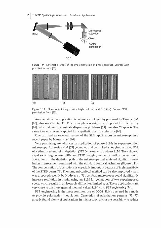
For application in the imaging light path, LCOS SLMs were used in implementa-tions of a phase contrast microscope [63–65], where addressing of different phasepatterns to the SLM located in the Fourier plane allowed to get phase contrast, DIC(differential interference contrast), and dark field images in the same microscope(Figure 1.9). Figure 1.10 shows a phase bar structure imaged in bright field inpanel (a) and SLM-based DIC in panels (b and c). The difference between two DICimages in Figure 1.10 represents two different periods of the gratings used for DIC.
16 1 LCOS Spatial Light Modulators: Trends and Applications
SLM
CCD
Object
Microscopeobjective
Köhlerillumination
Figure 1.9 Schematic layout of the implementation of phase contrast. Source: Withpermission from [63].
(a) (b) (c)
Figure 1.10 Phase object imaged with bright field (a) and DIC (b,c). Source: Withpermission from [63].
Another attractive application is coherence holography proposed by Takeda et al.[66], also see Chapter 11. This principle was originally proposed for microscopy[67], which allows to eliminate dispersion problems [68], see also Chapter 6. Thesame idea was recently applied for a synthetic aperture telescope [69].
One can find an excellent review of the SLM applications in microscopy in arecent paper by Maurer et al. [70].
Very promising are advances in application of phase SLMs in superresolutionmicroscopy. Auksorius et al. [72] generated and controlled a doughnut-shaped PSFof a stimulated emission depletion (STED) beam with a phase SLM. They showedrapid switching between different STED imaging modes as well as correction ofaberrations in the depletion path of the microscope and achieved significant reso-lution improvement compared with the standard confocal technique (Figure 1.11).The compensation of aberrations is especially important because of high sensitivityof the STED beam [71]. The standard confocal method can be also improved – as itwas proposed recently by Mudry et al. [73], confocal microscopes could significantlyincrease resolution in z-axis, using an SLM for generation of two superimposedspots, which results in an isotropic diffraction-limited spot. These applications arevery close to the more general method, called SLM-based PSF engineering [74].
PSF engineering is the most common use of LCOS SLMs operated in a modeto provide polarization modulation. Generation of polarization patterns [75–77]already found plenty of applications in microscopy, giving the possibility to reduce

1.3 Some Applications of Spatial Light Modulators in Optical Imaging and Metrology 17
1
1 1.5
0.5
0.50
0
1
1−1
0.5
0.5−0.50
0
273 nm
220 nm
150 nm
0.34 μm
0.73 μmConf.
Typel
Typell
x (μm) z (μm)
1 μm
(a)
(d)
(b)
(e)
(c)
(f)
(g) (h)
x
x
z
y
Figure 1.11 (a,b,c) Lateral and (d,e,f) axialfluorescence images of 200 nm beads with(a,d) confocal acquisition, (b,e) acquisitionwith a doughnut STED beam (type I), and(c,f) acquisition with a ‘‘bottle’’ STED beam(type II). (g,h) Normalized intensity line pro-files of lateral and axial images, respectively,
with specified FWHM. Insets show the cor-responding PSFs. Note the differences in lat-eral and axial resolution between two STEDimaging modes. (Source: With permissionfrom [71]). (Please find a color version ofthis figure on the color plates.)
a spot size [78], to generate a doughnut, an optical bubble [79], or needle [80].Generation of the doughnut could also be achieved with spiral phase patternwithout additional polarization components (e.g., QWPs) as it was discussed ear-lier [72, 81]. Beversluis and Stranick [82] showed independent polarization andphase modulation with two SLMs, which succeeded in increasing the contrast of300 nm polystyrene beads in coherent anti-Stokes Raman spectroscopy (CARS)images. They used independent phase and polarization modulation (Figure 1.12)for PSF engineering (Figure 1.13, see also [74]). SLM 1 in Figure 1.12 performsphase-only modulation of the light wave. SLM 2 with attached QWP is dedi-cated to polarization-only modulation. These two SLMs with optics form a ‘‘modeconverter,’’ so that finally phase- and polarization-modulated wavefronts are tele-centrically imaged in the pupil plane of the microobjective lenses. The differencesbetween linear, azimuthal, and radial polarizations showed in Figure 1.13 areobvious. Note also the changes in the Z-component of the field.
The methods and applications of PSF engineering were recently reviewed byZhan [83].

18 1 LCOS Spatial Light Modulators: Trends and Applications
Modeconverter
Laser514 nm
Spatial filter ND Pol. l/2APD
Relay telescope
SLM image plane
Single molecule sample on xyz -stage
Ex. filterPupilplane
Dichroicmirror
Em.filter
Berek compensator
fxy
qxy
2f2
f2
2f1
f1f 1SLM 1
SLM 245 l/4Mode converter
Figure 1.12 Schematic layout of the phase and polarization modulation in aPSF-engineered microscope. Source: With permission from [74].
(a) Linear X (b) Azimuthal (C) Radial
z
y
x
Dip
ole
axis
orie
ntat
ion
Theory TheoryExp Exp Theory Exp
Figure 1.13 Theoretical and experimental images for (a) linear, (b) azimuthal, and(c) radial pupil polarizations (each image has 2 μm side). Source: With permissionfrom [74].

1.3 Some Applications of Spatial Light Modulators in Optical Imaging and Metrology 19
G
FL
M2
M1
2D LCOS SLM
(a) (b) (c)
Figure 1.14 Femtosecond pulse shaper. (a) Schematic layout. G, diffraction grating; M1and M2, mirrors; FL, Fourier lens. (b) Amplitude modulation with SLM. (c) Phase modula-tion with SLM. Source: With permission from [84].
760 770 780 790 800 810 820 830 840
l (nm)
1
0.5
0
Spe
ctra
lin
tens
ity (
a.u.
)
Figure 1.15 Amplitude-only modulation of the spectrum. Source: With permission from[84].
Frumker and Silberberg [84] demonstrated amplitude and phase shaping offemtosecond laser pulse using an LCOS phase modulator (Figure 1.14a). Hereillumination femtosecond pulses are split into a spectrum with help of a grating Gso that a cylindrical Fourier lens FL focuses each wavelength component onto theSLM in only one direction. The components stay in the same time spread in verticaldirection. Then, writing a phase grating in vertical direction (Figure 1.14b) allowsto modulate amplitude of the spectral components (Figure 1.15) independent of thephase modulation (the last one uses SLM in horizontal direction – Figure 1.14c).The phase modulation is observed as a correlation function showed at Figure 1.16.A principle capability of LCOS to work in the near-infrared range allowed todevelop a telecommunication device based on a similar principle, combiningoptical switching [85] and pulse shaping capabilities of SLMs [86]. A similarapproach was recently patented and commercialized by Finisar [87].
There are several attempts to use SLM for holographic reconstruction in visualsystems. A comprehensive review of SLM-based holographic 3D displays is given byOnural et al. [89]. SeeReal Technologies demonstrated an 8 in. full color holographicprojection 3D display (Figures 1.17 and 1.18) using an amplitude SLM andobservation through a concave mirror – ‘‘display’’ [88]. The color was achieved usingcolor field sequential technology. The holograms were a kind of Fresnel hologram,where complex values were converted to amplitude values using well-known

20 1 LCOS Spatial Light Modulators: Trends and Applications
1
1 1.5 2 2.5 3
1 1.5 2 2.5 3
1 1.5 2 2.5 3
0
1
0
1
0
Time (ps)
Cro
ss-c
orre
latio
n (a
.u.)
(a)
(b)
(c)
Figure 1.16 Cross-correlation. (a) No phase is applied. (b) Periodic phase-only modulationwith binary modulation depth of π/2 and period 3.1 THz.(c) Periodic phase-onlymodulation with modulation depth of π . Source: With permission from [84].
Display
SLM
Beamexpander
Dichroicmirrors
Laser red
Laser blueLasergreen
Mirror
Mirror
Beamsplitter
Telecentriclenses
Projectionlenses
Viewingwindow
Figure 1.17 Schematic layout of 3D projection display. Source: With permission from [88].
Burckhardt or detour phase encoding [35]. A significant drawback of the system isits relatively low light efficiency, caused by the usage of an amplitude SLM. This isan unusual example of using amplitude modulation in digital holography, as 3Ddisplays of this kind are thought to be realized with a phase modulator. However,

1.3 Some Applications of Spatial Light Modulators in Optical Imaging and Metrology 21
Figure 1.18 Photo of the display. (Source: With permission from [88]). (Please find a colorversion of this figure on the color plates.)
here the amplitude modulation provided good-quality reconstructions and helpedto omit iterative calculations at the same time.
Light Blue Optics introduced full color 2D holographic projection unit withferroelectric SLMs [90]. They demonstrated good quality of reconstructions, usinghigh frame rate of ferroelectric SLMs to suppress perceivable speckle noise.Unfortunately, due to the nature of ferroelectric LCs, as it was already mentionedabove, this approach shows relatively low light efficiency.
An implementation of the holographic visualization in the head mounted display(HMD) looks quite attractive as well. The features would be high brightness andcapability of 3D representing information or objects overlapped with real objects(see-through). The reconstructed information can be adapted to the individual ob-server using the wavefront correction properties and thus will allow to compensatemyopia or hyperopia, astigmatic errors of the eye, as well as other aberrations upto ‘‘supernormal vision’’ level as it was demonstrated by Liang et al. [91].
The basic layouts for the HMD can be different, e.g., projection of the SLMinto the eye pupil, as it was already demonstrated for head-up display [92] orthe projection of the Fourier transform of the SLM, as it was made in theprojection holographic display of SeeReal Technologies (see earlier discussion).Main parameters of the HMD are the exit pupil and the FOV. Simple analysisshows that the product of the FOV and exit pupil in a digital holographic HMD is aninvariant quantity that is proportional to the number of pixels at the SLM, regardlessof the scheme used (as long as no pupil expander is used). This means that visualholographic systems are very critical to pixel count so that system becomes feasibleonly if the pixel amount exceeds 2–4 megapixels. Figures 1.19 and 1.20 showreconstructions from a prototype of a digital holographic see-through HMD, basedon phase-only HOLOEYE SLM of the high-definition television (HDTV) resolutionand a fiber-coupled red superluminescent diode. The numerical aperture of thecamera was matched to that of the human eye. This ensures similarity of specklecharacteristics between the captured pattern and the pattern perceived by the

22 1 LCOS Spatial Light Modulators: Trends and Applications
(a) (b)
Figure 1.19 Reconstruction of a hologram, captured at two reconstruction distances. TheFOV is ≈6◦ in horizontal and 3.4◦ in vertical direction. The exit pupil is 12 mm. Note thedifference in acuity of the background. (a) Fuel sign. (b) Stop sign.
Figure 1.20 Reconstruction of a resolution test target. Field of view is ≈14◦.
human eye [93]. The SLM is projected in the exit pupil plane with help of atelecentric system. The observer’s eye makes a Fourier transform and gets animage at the retina. Figure 1.19a,b is the reconstruction from the same hologram.The hologram contains 3D information, which is reconstructed in two differentplanes. Another example shows approximately 14◦ field of view (Figure 1.20), wherethe eye can resolve a finer pattern.
The 3D display application, realized as an array of phase SLMs with Fresnelholograms, is given in Chapter 3. The readers are also referred to Chapter 2 for ageneral overview of the 3D display technologies.
In addition to the more established fields of applications such as microscopy,metrology, and holographic visualization, there is an apparently ever-growingnumber of other fields in which the potential benefits of using SLMs are expected.It can relate to optical processing of the information; for example, Marcheseet al. [94] designed an SLM-based optronic processor for rapid processing of thesynthetic-aperture radar (SAR) multilook images. As an adaptive optics example,Vellekoop and Mosk [95] focused light through a highly scattering medium. Thereare a number of scientific works, related to quantum optics. Becker et al. [96]
References 23
applied amplitude SLM to generate dark solitons in Bose–Einstein Condensate(BEC), whereas another group manipulated BEC with a ferroelectric phase SLM[97]. Bromberg et al. [98] implemented computational ghost imaging with only asingle bucket detector, where the rotating diffuser was replaced with a phase SLM,thus allowing the computation of the propagating field and omitting the usage ofthe second high-resolution detector. Stutz et al. [99] generated, manipulated, anddetected multidimensional entangled photons with a phase SLM. Following himLima et al. [100] demonstrated manipulation with spatial qudit (‘‘multilevel qubit’’)states.
1.4Conclusion
LC-based SLMs have existed for the past 40 years and have been a basis for manystudies in electro-optical effects. With the reflective LCOS microdisplay technology,one could realize components with parameters, unthought before (e.g., resolution,pixel size, fill factor, overall light efficiency, and driving electronics solutions).
Even though projection display and SLM target markets are quite different, trendsin the LCOS microdisplay technology fit to some extent the requirements of SLMdevelopment. This fact, the accessibility of the technology, and the possibility ofcustomization of the parameters also lead to considerably smaller investments. Thebackground in consumer products also ensures achievement of stable, predictable,and high-performance commercial products with competitive pricing.
The availability of such SLMs has helped the scientific community to explore awide range of potential applications. High-resolution devices were made possible,but for phase modulators, high diffraction efficiency along with high framerate is still a challenge. Customization including SLM-specific backplane designtogether with mass-production-suitable production facilities opens the way forimplementation in various commercial applications.
Current developments will bring 10 megapixel phase-only panels (e.g., 4160 ×2464 pixels) to the market. Pixel size will drop down further below 4 μm. Thecontinuous progress in the development of driving electronics makes higherrefresh rates available, together with a reduction of digital-specific noise. This willpositively influence feasibility of SLMs for industrial applications.
Although LCOS SLMs have originally found their applications in scientificresearch, there is an increased interest in the commercial field and a transitionfrom science to industry is expected in the near future.
References
1. Solgaard, O. (2009) Photonic microsys-tems: micro and nanotechnology appliedto optical devices and systems, Springer.
2. Armitage, D., Underwood, I., andWu, S.-T. (2006) Introduction to
Microdisplays, John Wiley & Sons,Ltd, Chichester.
3. Knipe, R.L. (1996) Challenges of a dig-ital micromirror device: modeling anddesign. SPIE Proceedings Micro-Optical

24 1 LCOS Spatial Light Modulators: Trends and Applications
Technologies for Measurement,Sensors, and Microsystems, vol. 2783,pp. 135–145. doi: 10.1117/12.248483.
4. Amm, D.T. and Corrigan, R.W. (1998)Grating light valve technology: Updateand novel applications. SID Symp.Dig. Tech. Pap., 29 (1), 29–32. doi:10.1889/1.1833752.
5. Schenk, H., Wolter, A., Dauderstaedt,U., Gehner, A., and Lakner, H. (2005)Micro-opto-electro-mechanical sys-tems technology and its impact onphotonic applications. J. Microlith. Mi-crofab. Microsyst., 4 (4), 041501. doi:10.1117/1.2131824.
6. Lopez, D., Aksyuk, V.A., Watson,G.P., Mansfield, W.M., Cirelli, R.,Klemens, F., Pardo, F., Ferry, E.,Miner, J., Sorsch, T.W., Peabody, M.,Bower, J., Peabody, M., Pai, C.S.,and Gates, J. (2007) Two-dimensionalMEMS array for maskless lithographyand wavefront modulation. SPIE Proc.,6589,. doi: 10.1117/12.724467.
7. Lapisa, M., Zimmer, F., Niklaus, F.,Gehner, A., and Stemme, G.(2009) Cmos-integrable piston-typemicro-mirror array for adaptive op-tics made of mono-crystalline siliconusing 3-d integration. Proceedings ofthe IEEE International Conference onMicro Electro Mechanical Systems,pp. 1007–1010.
8. Doucet, M., Picard, F., Niall, K.K., andJerominek, H. (2005) Operation modesfor a linear array of optical flexiblereflective analog modulators. SPIE Pro-ceedings Cockpit and Future Displaysfor Defense and Security, vol. 5801,pp. 219–233. doi: 10.1117/12.604059.
9. Melcher, R.L. (2000) LCoS microdisplaytechnology and applications. Inform.Display, 16 (7), 20–23.
10. Fournier, F.R. and Rolland, J.P. (2008)Design methodology for high bright-ness projectors. J. Display Technol., 4(1), 86–91.
11. Sterling, R. (2008) JVC D-ILA highresolution, high contrast projectors andapplications. Proceedings of the 2008Workshop on Immersive Projection Tech-nologies/Emerging Display Technologies,ACM, New York USA, pp. 10: 1–10:6.
IPT/EDT ’08, ISBN 978-1-60558-212-2.doi: 10.1145/1394669.1394684.
12. Fujitsu Semiconductor Ltd (2007)Wafer foundry service. FIND Vol.25No.1.
13. Neil Savage (2009) Digital spatiallight modulators. Nat. Photon., 3 (3),170–172.
14. Cuypers, D., Van Doorselaer, G.,Van Den Steen, J., De Smet, H., andVan Calster, A. (2002) Assembly ofan XGA 0.9 LCOS display using in-organic alignment layers for VANLC. Conf. Rec. Int. Disp. Res. Conf.,Society for Information Display (SID),pp. 551–554.
15. Gandhi, J., Anderson, J.E., andStefanov, M.E. (2001) Experimentalcomparison of contrast ratio vs. f/# forvarious reflective LCoS modes. SIDSymp. Dig. Tech. Pap., 32 (1), 326–329.doi: 10.1889/1.1831862.
16. Osten, S., Kruger, S., andHermerschmidt, A. (2008) NewHDTV (1920 × 1080) phase-onlySLM, in Adaptive Optics for Industryand Medicine (ed. C. Dainty), SPIE,pp. 124–129.
17. Marquez, A., Iemmi, C., Moreno,I., Campos, J., and Yzuel, M. (2005)Anamorphic and spatial frequencydependent phase modulation on liq-uid crystal displays. optimization ofthe modulation diffraction efficiency.Opt. Express, 13 (6), 2111–2119. doi:10.1364/OPEX.13.002111.
18. Karl Waterman, J. (2007) Display driverarchitecture for a liquid crystal dis-play and method therefore. US Patent7161570.
19. Worley, S.W. and Hong Chow, W.(2010) System and method for reduc-ing inter-pixel distortion by dynamicredefenition of display segment bound-aries. EP Patent 1093653 B1.
20. Spencer Worley, W., Lyle Hudson, E.,and Hong Chow, W. (2008) Displaywith multiplexed pixels and driv-ing methods. US Patent Application2008/0225030.
21. Shurcliff, W.A. (1962) Polarized Light,Production and Use, Harvard UniversityPress.

References 25
22. Robinson, M., Sharp, G., and Chen, J.(2005) Polarization Engineering for LCDProjection, John Wiley & Sons, Ltd,Chichester.
23. Yariv, A. and Yeh, P. (1984) OpticalWaves in Crystals, John Wiley & Sons,Inc., New York.
24. Hermerschmidt, A., Quiram, S.,Kallmeyer, F., and Eichler, H.J.(2007) Determination of the Jonesmatrix of an LC cell and derivationof the physical parameters of theLC molecules. SPIE Proc, 6587,. doi:10.1117/12.722895.
25. Duelli, M., Shemo, D.M., Hendrix,K.D., Ledeur, A., and Tan, K.L. (2005)High performance contrast enhancingfilms for VAN-mode LCOS panels.SID Sympo. Dig. Tech. Pap., 36 (1),892–895. doi: 10.1889/1.2036592.
26. Tan, K.L., Hendrix, K.D., Duelli, M.,Shemo, D.M., Ledeur, A., Zieba, J.,and Greenberg, M. (2005) Design andcharacterization of a compensator forhigh contrast LCoS projection systems.SID Symp. Dig. Tech. Pap., 36 (1),1810–1813. doi: 10.1889/1.2036370.
27. Davis, J.A., Moreno, I., and Tsai, P.(1998) Polarization eigenstates fortwisted-nematic liquid-crystal displays.Appl. Opt., 37 (5), 937–945.
28. Clemente, P., Duran, V.,Martınez-Leon, Ll., Climent, V.,Tajahuerce, E., and Lancis, J. (2008)Use of polar decomposition of Muellermatrices for optimizing the phase re-sponse of a liquid-crystal-on-silicon dis-play. Opt. Express, 16 (3), 1965–1974.
29. Milewski, G., Engstrom, D., andBengtsson, J. (2007) Diffractive opticalelements designed for highly precisefar-field generation in the presence ofartifacts typical for pixelated spatiallight modulators. Appl. Opt., 46 (1),95–105. doi: 10.1364/AO.46.000095.
30. Georgiou, A., Christmas, J.,Collings, N., Moore, J., and Crossland,W.A. (2008) Aspects of hologramcalculation for video frames. J. Opt.A: Pure Appl. Op., 10, 035302. doi:10.1088/1464-4258/10/3/035302.
31. Hermerschmidt, A., Kruger, S., andWernicke, G. (2007a) Binary diffractivebeam splitters with arbitrary diffraction
angles. Opt. Lett., 32 (5), 448–450. doi:10.1364/OL.32.000448.
32. Persson, M., Engstrom, D., Frank, A.,Backsten, J., Bengtsson, J., andGoksor, M. (2010) Minimizing in-tensity fluctuations in dynamicholographic optical tweezers byrestricted phase change. Opt. Ex-press, 18 (11), 11250–11263. doi:10.1364/OE.18.011250.
33. Birch, P.M., Young, R., Budgett, D.,and Chatwin, C. (2000) Two-pixelcomputer-generated hologram witha zero-twist nematic liquid-crystalspatial light modulator. Opt.Lett., 25 (14), 1013–1015. doi:10.1364/OL.25.001013.
34. Futterer, G., Leister, N., Haussler,R., and Lazarev, G. (2010)Three-dimensional light modulationarrangement for modulating a wavefield having complex information.Patent Application WO 2010/149588A1.
35. Burckhardt, C.B. (1970) A simpli-fication of Lee’s method of gen-erating holograms by computer.Appl. Opt., 9 (8), 1949–1949. doi:10.1364/AO.9.001949.
36. van Putten, E.G., Vellekoop, I.M.,and Mosk, A.P. (2008) Spatial am-plitude and phase modulation usingcommercial twisted nematic LCDs.Appl. Opt., 47 (12), 2076–2081. doi:10.1364/AO.47.002076.
37. Rosen, J. and Brooker, G. (2007)Digital spatially incoherent Fresnelholography. Opt. Lett., 32 (8), 912–914.doi: 10.1364/OL.32.000912.
38. Hermerschmidt, A., Osten, S., Kruger,S., and Blumel, T. (2007) Wave frontgeneration using a phase-only modu-lating liquid-crystal-based micro-displaywith hdtv resolution. SPIE Proceed-ings, Adaptive Optics for Laser Systemsand Other Applications, vol. 6584,p. 65840E. doi: 10.1117/12.722891.
39. Emery, Y., Cuche, E., Marquet, F.,Aspert, N., Marquet, P., Kuhn, J.,Colomb, T., Montfort, F., Charriere,F., Depeursinge, C., Debergh, P., andConde, R. (2006) Digital holographicmicroscopy (dhm) for metrology anddynamic characterization of mems and

26 1 LCOS Spatial Light Modulators: Trends and Applications
moems. SPIE Proc., 6186, 61860 N. doi:10.1117/12.660029.
40. Kohler, C., Haist, T., Schwab, X., andOsten, W. (2008) Hologram optimiza-tion for slm-based reconstruction withregard to polarization effects. Opt.Express, 16 (19), 14853–14861. doi:10.1364/OE.16.014853.
41. Kohler, C., Haist, T., and Osten, W.(2009) Model-free method for measur-ing the full Jones matrix of reflectiveliquid-crystal displays. Opt. Eng., 48 (4),044002. doi: 10.1117/1.3119309.
42. Meeser, T., von Kopylow, C., andFalldorf, C. (2010) Advanced digi-tal lensless Fourier holography bymeans of a spatial light modulator.3DTV-Conference: The True Vision -Capture, Transmission and Display of3D Video (3DTV-CON), 2010, pp. 1–4,79.
43. Falldorf, C., Klattenhoff, R., andGesierich, A. (2009) Lateral shear-ing interferometer based on a spatiallight modulator in the Fourier plane, inFringe 2009: 6th International Workshopon Advanced Optical Metrology (eds W.,Osten and M. Kujawinska), SpringerHeidelberg, pp. 93–98.
44. Schaal, F., Warber, M., Rembe, C.,Haist, T., and Osten, W. (2009) Dy-namic multipoint vibrometry usingspatial light modulators, in Fringe 2009,6th International Workshop on AdvancedOptical Metrology (eds M. Osten and W.Kujawinska), Springer, pp. 528–531.
45. Baumbach, T., Osten, W., vonKopylow, C., and Juptner, W. (2006)Remote metrology by comparativedigital holography. Appl. Opt., 45 (5),925–934. doi: 10.1364/AO.45.000925.
46. Jenness, N.J. (2009) Three-dimensionalholographic lithography and manipu-lation using a spatial light modulator.PhD thesis. Duke University.
47. Jenness, N.J., Wulff, K.D., Johannes,M.S., Padgett, M.J., Cole, D.G., andClark, R.L. (2008) Three-dimensionalparallel holographic micropatterningusing a spatial light modulator. Opt.Express, 16 (20), 15942–15948. doi:10.1364/OE.16.015942.
48. Jenness, N.J., Hill, R.T., Hucknall, A.,Chilkoti, A., and Clark, R.L. (2010)
A versatile diffractive masklesslithography for single-shot andserial microfabrication. Opt. Ex-press, 18 (11), 11754–11762. doi:10.1364/OE.18.011754.
49. Li, J., Wen, C.-H., Gauza, S., Lu, R.,and Wu, S.-T. (2005) Refractive in-dices of liquid crystals for displayapplications. J. Display Technol., 1 (1),51.
50. Gauza, S., Wen, C.-H., Tan, B.,and Wu, S.-T. (2004) UV stablehigh birefringence liquid crystals.Jpn. J. Appl. Phys., 43, 7176–+. doi:10.1143/JJAP.43.7176.
51. von Freymann, G., Ledermann, A.,Thiel, M., Staude, I., Essig, S.,Busch, K., and Wegener, M. (2010)Three-dimensional nanostructuresfor photonics. Adv. Funct. Mater., 20(7), 1038–1052. ISSN 1616-3028. doi:10.1002/adfm.200901838.
52. Nikolenko, V., Watson, B.O., Araya, R.,Woodruff, A., Peterka, D.S., andYuste, R. (2008) SLM microscopy:scanless two-photon imaging andphotostimulation with spatial lightmodulators. Front Neural Circuits, 2 (5),1–14.
53. Fratz, M., Fischer, P., and Giel, D.M.(2009) Full phase and amplitude con-trol in computer-generated holography.Opt. Lett., 34 (23), 3659–3661. doi:10.1364/OL.34.003659.
54. Kuang, Z., Perrie, W., Liu, D.,Edwardson, S., Cheng, J., Dearden, G.,and Watkins, K. (2009) Diffrac-tive multi-beam surface micro-processing using 10 ps laserpulses. Appl. Surf. Sci., 255 (22),9040–9044. ISSN 0169-4332. doi:10.1016/j.apsusc.2009.06.089.
55. Hermerschmidt, A., Kruger, S.,Haist, T., Zwick, S., Warber, M., andOsten, W. (2007c) Holographic opticaltweezers with real-time hologram cal-culation using a phase-only modulatingLCOS-based SLM at 1064 nm. SPIEProc., 6905,. doi: 10.1117/12.764649.
56. Hirvonen, L., Wicker, K., Mandula, O.,and Heintzmann, R. (2009) Struc-tured illumination microscopy ofa living cell. Eur. Biophys. J., 38,

References 27
807–812. ISSN 0175-7571. doi:10.1007/s00249-009-0501-6.
57. Chang, B.-J., Chou, L.-J., Chang, Y.-C.,and Chiang, S.-Y. (2009) Isotropicimage in structured illumination mi-croscopy patterned with a spatial lightmodulator. Opt. Express, 17, 14710–+.doi: 10.1364/OE.17.014710.
58. Heintzmann, R. (2003) Saturatedpatterned excitation microscopywith two-dimensional excitation pat-terns. Micron, 34 (9), 283–291. doi:10.1016/S0968-4328(03)00053-2.
59. Hayasaki, Y., Sumi, S., Mutoh, K.,Suzuki, S., Itoh, M., Yatagai, T., andNishida, N. (1996) Optical manipula-tion of microparticles using diffractiveoptical elements, in SPIE Proceedings,vol. 2778, (eds J.-S. Chang, J.-H. Lee,S.-Y. Lee, and C.H. Nam), SPIE, pp.229–+.
60. Dufresne, E.R. and Grier, D.G. (1998)Optical tweezer arrays and optical sub-strates created with diffractive optics.Rev. Sci. Instrum., 69, 1974–1977. doi:10.1063/1.1148883.
61. Reicherter, M., Haist, T., Wagemann,E.U., and Tiziani, H.J. (1999)Optical particle trapping withcomputer-generated hologramswritten on a liquid-crystal display.Opt. Lett., 24 (9), 608–610. doi:10.1364/OL.24.000608.
62. Haist, T., Zwick, S., Warber, M., andOsten, W. (2006) Spatial light modu-lators - versatile tools for holography.J. Hologr. Speckle, 3 (12), 125–136. doi:doi:10.1166/jhs.2006.019.
63. Zwick, S., Warber, M., Gorski, W.,Haist, T., and Osten, W. (2009) Flexibleadaptive phase contrast methods usinga spatial light modulator. ProceedingsDGAO, vol. A3.
64. Situ, G., Warber, M., Pedrini, G., andOsten, W. (2010) Phase contrast en-hancement in microscopy using spiralphase filtering. Opt. Commun., 283(7), 1273–1277. ISSN 0030-4018. doi:10.1016/j.optcom.2009.11.084.
65. Warber, M., Zwick, S., Hasler, M.,Haist, T., and Osten, W. (2009)SLM-based phase-contrast filter-ing for single and multiple imageacquisition, in SPIE Proceedings,
Optics and Photonics for Informa-tion Processing III, vol. 7442, (K.M.Iftekharuddin and A.A.S. Awwal),SPIE. doi: 10.1117/12.825945.
66. Takeda, M., Wang, W., and Nai,D.N. (2009) Coherence holography:a thought on synthesis and analysis ofoptical coherence fields, in Fringe 2009,6th International Workshop on AdvancedOptical Metrology (eds M. Osten and W.Kujawinska), Springer, pp. 14–+.
67. Rosen, J. and Brooker, G. (2008)Non-scanning motionless fluores-cence three-dimensional holographicmicroscopy. Nat. Photonics, 2, 190–195.doi: 10.1038/nphoton.2007.300.
68. Brooker, G., Siegel, N., Wang,V., and Rosen, J. (2011) Optimalresolution in Fresnel incoherentcorrelation holographic fluorescencemicroscopy. Opt. Express, 19, 5047–+.doi: 10.1364/OE.19.005047.
69. Katz, B. and Rosen, J. (2011) CouldSAFE concept be applied for de-signing a new synthetic aperturetelescope? Opt. Express, 19, 4924–+.doi: 10.1364/OE.19.004924.
70. Maurer, C., Jesacher, A., Bernet, S.,and Ritsch-Marte, M. (2011) What spa-tial light modulators can do for opticalmicroscopy. Laser & Photonics Rev.,5 (1), 81–101. ISSN 1863-8899. doi:10.1002/lpor.200900047.
71. Auksorius, E. (2008) Multidimen-sional fluorescence imaging andsuper-resolution exploiting ultrafastlaser and supercontinuum technology.PhD thesis. Imperial College London.
72. Auksorius, E., Boruah, B.R., Dunsby,C., Lanigan, P.M.P., Kennedy, G.,Neil, M.A.A., and French, P.M.W.(2008) Stimulated emission depletionmicroscopy with a supercontinuumsource and fluorescence lifetime imag-ing. Opt. Lett., 33 (2), 113–115. doi:10.1364/OL.33.000113.
73. Mudry, E., Le Moal, E., Ferrand, P.,Chaumet, P.C., and Sentenac, A. (2010)Isotropic diffraction-limited focusingusing a single objective lens. Phys.Rev. Lett., 105 (20), 203903–+. doi:10.1103/PhysRevLett.105.203903.

28 1 LCOS Spatial Light Modulators: Trends and Applications
74. Beversluis, M.R., Novotny, L., andStranick, S.J. (2006) Programmable vec-tor point-spread function engineering.Opt. Express, 14 (7), 2650–2656. doi:10.1364/OE.14.002650.
75. Chen, H., Zheng, Z., Zhang, B.-F.,Ding, J., and Wang, H.-T. (2010)Polarization structuring of focusedfield through polarization-onlymodulation of incident beam.Opt. Lett., 35 (16), 2825–2827. doi:10.1364/OL.35.002825.
76. Wang, X.-L., Ding, J., Ni, W.-J., Guo,C.-S., and Wang, H.-T. (2007) Gener-ation of arbitrary vector beams witha spatial light modulator and a com-mon path interferometric arrangement.Opt. Lett., 32 (24), 3549–3551. doi:10.1364/OL.32.003549.
77. Chen, W. and Zhan, Q. (2010) Diffrac-tion limited focusing with controllablearbitrary three-dimensional polariza-tion. J. Opt., 12 (4), 045707.
78. Dorn, R., Quabis, S., and Leuchs, G.(2003) Sharper focus for a radiallypolarized light beam. Phys. Rev. Lett.,91 (23), 233901–+. doi: 10.1103/Phys-RevLett.91.233901.
79. Chen, W. (2009) Focus engineeringwith spatially variant polarization fornanometer scale applications. PhDthesis. The School of Engineering ofthe University of Dayton.
80. Wang, H., Shi, L., Lukyanchuk, B.,Sheppard, C., and Chong, C.T. (2008)Creation of a needle of longitudinallypolarized light in vacuum using binaryoptics. Nat. Photonics, 2, 501–505. doi:10.1038/nphoton.2008.127.
81. Bashkansky, M., Park, D., and Fatemi,F.K. (2010) Azimuthally and radiallypolarized light with a nematic SLM.Opt. Express, 18 (1), 212–217. doi:10.1364/OE.18.000212.
82. Beversluis, M.R. and Stranick, S.J.(2008) Enhanced contrast coherentanti-Stokes Raman scattering mi-croscopy using annular phase masks.Appl. Phys. Lett., 93 (23), 231115–+.doi: 10.1063/1.3046719.
83. Zhan, Q. (2009) Cylindrical vectorbeams: from mathematical concepts toapplications. Adv. Opt. Photon., 1 (1),1–57. doi: 10.1364/AOP.1.000001.
84. Frumker, E. and Silberberg, Y. (2007)Phase and amplitude pulse shap-ing with two-dimensional phase-onlyspatial light modulators. J. Opt. Soc.Am. B, 24 (12), 2940–2947. doi:10.1364/JOSAB.24.002940.
85. Kali, A., Tan, A., Gravey, P.,Wolffer, N., Lelah, A., andPincemin, E. (2003) Assessment ofLCOS technology for the realization ofscalable n×n optical switches. Proceed-ings of International Conference onPhotonics in Switching (PS 2003).
86. Roelens, M.A., Bolger, J.A.,Williams, D., and Eggleton, B.J.(2008) Multi-wavelength synchronouspulse burst generation with awavelength selective switch. Opt.Express, 16 (14), 10152–10157. doi:10.1364/OE.16.010152.
87. Frisken, S.J. (2009) Optical communi-cations system. US Patent 7593608.
88. Leister, N., Schwerdtner, A.,Futterer, G., Buschbeck, S., Olaya,J.-C., and Flon, S. (2008) Full-color in-teractive holographic projection systemfor large 3D scene reconstruction. SPIEProc., 6911,. doi: 10.1117/12.761713.
89. Onural, L., Yaras, F., and Kang,H. (2010) Digital holographicthree-dimensional video dis-plays. Proc. IEEE, 99,. doi:10.1109/JPROC.2010.2098430.
90. Buckley, E. (2008) Holographic laserprojection technology. SID Symp. Dig.Tech. Pap., 39 (1), 1074–1079. doi:10.1889/1.3069321.
91. Liang, J., Williams, D.R., and Miller,D.T. (1997) Supernormal visionand high-resolution retinal imag-ing through adaptive optics. J. Opt.Soc. Am. A, 14 (11), 2884–2892. doi:10.1364/JOSAA.14.002884.
92. Hendricks, U., Kruger, S., Brandt, P.,Charle, H., and Sahlbom, D. (2008)Holographic information display. USPatent Application 2008/0192312 A1.
93. Goodman, J.W. (1976) Some funda-mental properties of speckle. J. Opt.Soc. Am., 66 (11), 1145–1150. doi:10.1364/JOSA.66.001145.
94. Marchese, L., Bourqui, P.,Turgeon, S., Doucet, M., Vachon, C.,Harnisch, B., Suess, M., Chateauneuf,
References 29
F., and Bergeron, A. (2010) A SARmultilook optronic processor for opera-tional Earth monitoring applications, inSPIE Proceedings, SAR Image Analysis,Modeling, and Techniques X, vol. 7829,(ed. C. Notarnicola), pp. 782904. doi:10.1117/12.866986.
95. Vellekoop, I.M. and Mosk, A.P. (2007)Focusing coherent light throughopaque strongly scattering media.Opt. Lett., 32 (16), 2309–2311.
96. Becker, C., Stellmer, S., Soltan-Panahi,P., Dorscher, S., Baumert, M., Richter,E.-M., Kronjager, J., Bongs, K., andSengstock, K. (2008) Oscillations andinteractions of dark and dark brightsolitons in Bose Einstein conden-sates. Nat. Phys., 4, 496–501. doi:10.1038/nphys962.
97. Boyer, V., Godun, R.M., Smirne, G.,Cassettari, D., Chandrashekar, C.M.,Deb, A.B., Laczik, Z.J., and Foot, C.J.(2006) Dynamic manipulation of
Bose–Einstein condensates with aspatial light modulator. Phys. Rev. A,73 (3), 031402–+. doi: 10.1103/Phys-RevA.73.031402.
98. Bromberg, Y., Katz, O., andSilberberg, Y. (2009) Ghost imagingwith a single detector. Phys. Rev. A,79 (5), 053840. doi: 10.1103/Phys-RevA.79.053840.
99. Stutz, M., Groblacher, S.,Jennewein, T., and Zeilinger, A.(2007) How to create and detectn-dimensional entangled photonswith an active phase hologram.Appl. Phys. Lett., 90 (26), 261114. doi:10.1063/1.2752728.
100. Lima, G., Vargas, A., Neves, L.,Guzman, R., and Saavedra, C. (2009)Manipulating spatial qudit states withprogrammable optical devices. Opt.Express, 17 (13), 10688–10696. doi:10.1364/OE.17.010688.
