1 in the name god advanced vlsi class presentation a 1.1ghz charge recovery logic insructor : dr....
TRANSCRIPT

1
IN THE NAME GOD
Advanced VLSI Class Presentation
A 1.1GHz Charge Recovery Logic
Insructor : Dr. FakhrayiPresented by : Mahdiyeh Mehran

2
Adopted From:A 1.1GHz
Charge Recovery Logic
Visvesh S. Sathe
Juang-Ying Chueh
Marios C. Papaefthymiou
University of Michigan, Ann Arbor, USA

3
Contributions
• First ever demonstration of fully integrated charge-recovery chip in 0.13m CMOS at GHz clock rates
– Boost Logic : Dynamic charge-recovery circuit family
• Chain of test gates (1600 gates total)
• Integrated inductor and clock generator
• Resonant operation at 850MHz, 1.3V
• Functional at 1.1GHz, 1.4V
• Energy recovery rate at resonance = 60%

4
Outline
• Charge Recovery – Brief overview
– Basic Principles
• Boost Logic structure
• Boost Logic operation
• Boost Logic test chip
• Chip measurement results

5
Brief Overview of Charge Recovery
Ref.[1]
• Gradual transition of power supply (Power-Clock).• Supply must enable recovery of charge.• Inductor used to resonate power clock.
2CVT
RCECR
Vin
VC
v
time
I
time
T
VC
+
-
VinVin
I
C C
R

6
Outline
• Charge Recovery – Brief overview
– Basic Principles
• Boost Logic structure
• Boost Logic operation
• Boost Logic test chip
• Chip measurement results

7
VC = Vdd’ – Vss’ = Vth
Vdd’ = (Vdd + Vth)/2
Vss’ = (Vdd - Vth)/2

8
Boost Logic: Hybrid Charge Recovery
Ref.[1]
• Two-stage operation : Logic and Boost• Logic Stage performs logical evaluation• Boost Stage takes output nodes to full rail.
BoostLogic Logic
f
foutout
Vdd’
Vss’
Vdd’
Vss’
in inout
Vdd/2
Vdd
Vss’
Vdd’
Logic Stage
time
Voltage
Vc≈Vth
out

9
Boost Logic: Hybrid Charge Recovery
BoostLogic Logic
f
foutout
Vdd’
Vss’
Vdd’
Vss’
in in
Boost Stage
Voltage
Vdd/2
Vdd
out
out
Vss’
Vdd’
Vc≈Vth
Ref.[1]
• Two-stage operation : Logic and Boost
• Logic Stage performs logical evaluation
• Boost Stage takes output nodes to full rail.

10
Boost Logic Structure
M1 M2
M3 M4
BOOST
ff
out
M6f
Vss’
Vdd’
Eval. Treeinputs
M5f
LOGIC
f
out
M8 f
Vss’
Vdd’
LOGIC
inputsEval. Tree
M7
Ref.[1]

11
Outline
• Charge Recovery – Brief overview
– Basic Principles
• Boost Logic structure
• Boost Logic operation
• Boost Logic test chip
• Chip measurement results
12
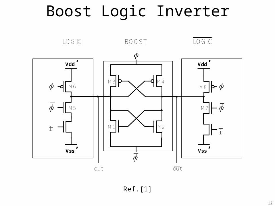
Boost Logic Inverter
f
out
M8 f
Vss’
Vdd’
LOGIC
M7
in
out
M6f
Vss’
Vdd’
M5f
LOGIC
in M1 M2
M3 M4
BOOST
ff
Ref.[1]

13
Boost Logic Operation
Ref.[1]
Boost Stage deactivated – all 4 devices in cutoff.• Clocked transistors turn on, enabling evaluation.• Logic stage drives output nodes to conventional rails.
0
1.2
t (s)
Vdd’
Vss’
0.6
Logic StageDrives Outputs
M1 M2
M3 M4
f
out
M8 f
Vss’
Vdd’
LOGIC
M7
in
out
BOOST
f
fM6f
Vss’
Vdd’
M5f
LOGIC
inf
fout
out

14
0
1.2
t (s)
Vdd’
Vss’
0.6
Both StagesTri-stated
M1 M2
M3 M4
f
out
M8 f
Vss’
Vdd’
LOGIC
M7
in
out
BOOST
f
fM6f
Vss’
Vdd’
M5f
LOGIC
in
Boost Logic Operation
Ref.[1]
• With f = Vss’ and f = Vdd’ clocked transistors turn off.
• Boost Stage remains tri-stated from output.• Pre-resolved output nodes provided to Boost Stage.
f
f

15
t (s)0
1.2
Vdd’
Vss’
0.6
Boost StageAmplifies Outputs
M1 M2
M3 M4
out
M8
M7
out
BOOST
f
fM6f
Vss’
Vdd’
M5f
LOGIC
in
f
f
Vss’
Vdd’
LOGIC
in
Boost Logic Operation
Ref.[1]
• As ff crosses Vdd’ (Vss’), Boost stage turns on. • Transistors M2 and M3 turn on.• Outputs track power clock.
f
out
out
f

16
0
1.2
t (s)
Vdd’
Vss’
0.6
Boost StageCharge Recovery
M1 M2
M3 M4
out
M8
M7
out
BOOST
f
fM6f
Vss’
Vdd’
M5f
LOGIC
in
f
f
Vss’
Vdd’
LOGIC
in
Boost Logic Operation
Ref.[1]
• As ff moves toward Vss(Vdd)– Transistors M2 and M3 turn on.– Charge in load capacitance returns to resonant clock.
• As V(out) – V(out) ≈ Vth, all 4 devices are in cutoff.
f
out
out
f

17
Cascade Simulation
Ref.[1]
• Logic cascaded with alternate clock phases.
• Vgs’ < 0 in logic evaluation trees when off.
• Low Vth devices desirable in logic evaluation trees.
Logic Boost(V)
0
0.5
1.0
t (s)
f
out
outin
in
0.5n 1n0n
f
f
f f
f
C = 1 FO4 Load
out
out
+
-
+
-
+
-
+
-
C
C
in
in i1i0

18
Outline
• Charge Recovery – Brief overview
– Basic Principles
– Previous work
• Issues with previous charge recovery logic
• Boost Logic structure
• Boost Logic operation
• Boost Logic test chip
• Chip measurement results

19
Boost Logic Test Chip
f
fClockGenerator
PulseGenerator
a
ba
b
reset
Signature Outputs
ProgrammableSchmitt Triggers
Boost Logic gate chains
a
ba
b
f
f
W
2W2W
2.4nH
W
Vdd
Vss
Progr.Delay
Progr. Delay
CLK
a
b 1/f1/2f
1/f
a
b
a
b
0<W<450m0%<D<50%
Ref.[1]
• Oscillation driven by reference clock.
• Programmable clock generator – Variable Duty Cycle 0%<D<50%
– Variable Switch Width 0<W<450µm

20
Boost Logic gate chains
Clock generator switches
Clock generator switches
Programmable Schmitt triggers
Boost Logic Test Chip : Die Shot
• Capacitance per phase = 29pF• Inductance = 2.4nH (2 layers, Cu, 0.7µm thick)

21
Outline
• Charge Recovery – Brief overview
– Basic Principles
– Previous work
• Issues with previous charge recovery logic
• Boost Logic structure
• Boost Logic operation
• Boost Logic test chip
• Chip measurement results
22
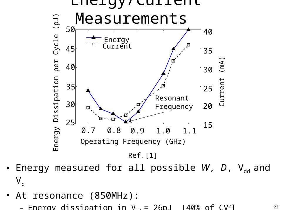
Energy/Current Measurements
Ref.[1]
• Energy measured for all possible W, D, Vdd and Vc
• At resonance (850MHz):– Energy dissipation in Vdd = 26pJ [40% of CV2]
– Energy dissipation in VC = 4pJ [VC = 0.45V]
Ene
rgy
Dis
sipa
tion
per
Cyc
le (
pJ)
Cur
rent
(m
A)
Operating Frequency (GHz)
EnergyCurrent
25
30
35
40
45
50
25
30
35
40
15
20
0.7 0.8 0.9 1.0 1.1
ResonantFrequency

23
Conclusion
• First ever charge-recovery test chip to exceed 1GHz clock rate
– Boost Logic : Dynamic charge-recovery circuit family
• Fully-integrated clock generator and inductor in 0.13m CMOS
• Functional up to 1.1GHz
• Resonant frequency = 850MHz
• Energy recovery rate at resonance = 60%

24
References
[1] V. S. Sathe, et al., “A 1.1GHz Charge-Recovery Logic,”ISSCC, pp.388-390, Feb., 2006.
[2] V. S. Sathe, et al., “A GHz-Class Charge Recovery Logic,” ISLPED, pp.91-94, Aug., 2005.
[3] S. Kim, et al., “True Single-Phase Adiabatic Circuitry,” Transactions on VLSI Systems, pp. 52-63, Feb., 2001.
[4] D. Suvakovic, C. Salama, “Two Phase Non-Overlapping Clock Adiabatic Differential Cascode Voltage Switch Logic (ADCVSL),” ISSCC Dig.Tech.Papers, pp. 364-365, Feb., 2000.
[5] D. Maksimovic, V. Oklobdzija, B. Nikolic, and K. Current “Clocked CMOS Adiabatic Logic with Integrated Single-Phase
Power-Clock Supply,”Transactions on VLSI Systems, Aug., 2000.

25