1 bit logic instructions
TRANSCRIPT

1 Bit Logic Instructions
1.1 Overview of Bit Logic Instructions
Description
Bit logic instructions work with two digits, 1 and 0. These two digits form the base of a number system called the binary system. The two digits 1 and 0 are calledbinary digits or bits. In conjunction with AND, OR, XOR and outputs, a 1 stands for logical YES and a 0 for logical NO.
The bit logic instructions interpret signal states of 1 and 0 and combine them according to Boolean logic. These combinations produce a result of 1 or 0 that is called the "result of logic operation" (RLO).
There are bit logic instructions to perform the following functions:
�� AND, OR and Exclusive OR: these instructions check the signal state and produce a result that is either copied to the RLO bit or combined with it.
�� AND-before-OR Logic Operation and OR-before-AND Logic Operation
�� Assign and Midline Output. these instructions assign the RLO or store it temporarily.
The following instructions react to an RLO of 1:
�� S : Set Output
�� R : Reset Output
�� SR : Set_Reset Flip Flop
�� RS : Reset_Set Flip Flop
Other instructions react to a positive or negative edge transition to perform the following functions:
�� N : Negative RLO Edge Detection
�� P : Positive RLO Edge Detection
�� NEG : Address Negative Edge Detection
�� POS : Address Positive Edge Detection
The remaining instructions affect the RLO directly in the following ways:
�� Insert Binary Input
�� Negate Binary Input
�� SAVE : Save RLO to BR Memory
Function Block Diagram (FBD) for S7-300 and S7-400 ProgrammingA5E00706955-01 1-1

Bit Logic Instructions
1.2 >=1 : OR Logic Operation
Symbol
>=1<address>
<address>
Parameter Data Type y AreaMemor Description
<address> BOOL I, Q, M, T, C, D,L
The address indicates the bit whosesignal state will be checked.
Descriptio
d the
oduces the result 0.
e
OR g of logic operationscombines the result of its signal state check with the value stored in the RLO bit.
se values are combined according to the OR truth table.
Status Word
BR CC1 CC0 OV OS OR STA RLO FC
n
With the OR instruction, you can check the signal states of two or more specifiedaddresses at the inputs of an OR box.
If the signal state of one of the addresses is 1, the condition is satisfied aninstruction produces the result 1. If the signal state of all addresses is 0, the condition is not satisfied and the instruction pr
If the OR instruction is the first instruction in a string of logic operations, it saves thresult of its signal state check in the RLO bit.
Each instruction that is not the first instruction in the strin
The
writes - - - - - X X X 1
Example
>=1I 0.0
I 0.1 =
Q 4.0
Output Q4.0 is set when the signal state is 1 at input I0.0 OR at input I0.1.
Function Block Diagram (FBD) for S7-300 and S7-400 Programming1-2 A5E00706955-01

Bit Logic Instructions
1.3 & : AND Logic Operation
Symbol
&<address>
<address>
Parameter Data Type Memory Area nDescriptio
<address> BOOL I, Q, M, T, C, D,L
The address indicates the bitwhose signal state will bechecked.
Descriptio
Every AND instruction that is not the first instruction in the string of logicoperations, combines the result of its signal state check with the value stored in the
O bit. These values are combined according to the AND truth table.
Status Word
BR CC1 CC0 OV OS OR STA RLO FC
n
With the AND instruction, you can check the signal states of two or more specifiedaddresses at the inputs of an AND box.
If the signal state of all operands is 1, the condition is satisfied and the instructionprovides the result 1. If the signal state of an address is 0, the condition is not satisfied and the instruction produces the result 0.
If the AND instruction is the first instruction in a string of logic operations, it savesthe result of its signal state check in the RLO bit.
RL
writes - - - - - X X X 1
Example
&I 0.0
I 0.1 =
Q 4.0
Output Q4.0 is set when the signal state is 1 at input I0.0 AND I0.1.
Function Block Diagram (FBD) for S7-300 and S7-400 ProgrammingA5E00706955-01 1-3

Bit Logic Instructions
1.4 AND-before-OR Logic Operation and OR-before-AND
Logic Operation
Description
With the AND-before-OR instruction, you can check the result of a signal state according to the OR truth table.
With an AND-before-OR logic operation the signal state is 1 when at least one AND logic operation is satisfied.
Status Word
BR CC1 CC0 OV OS OR STA RLO FC
writes - - - - - X X X 1
Example
&I 1.0
I 1.1 >=1
Q 3.1&I 1.2
I 1.3 =
The signal state is 1 at output Q3.1 when at least one AND logic operation istisfied
Descriptio
With the OR-before-AND instruction, you can check the result of a signal state check according to the AND truth table.
h an OR-before-AND logic operation the signal state is 1 when all OR logicperations are satisfied.
Status Word
BR CC1 CC0 OV OS OR STA RLO FC
sa
The signal state is 0 at output Q3.1 when no AND logic operation is satisfied.
n
Wito
writes - - - - - X X X 1
Function Block Diagram (FBD) for S7-300 and S7-400 Programming1-4 A5E00706955-01

Bit Logic Instructions
Example
>=1I 1.0
I 1.1
Q 3.1
&
I 1.2
I 1.3 =>=1
The signal state is 1 at output Q3.1 when both OR logic operations are satisfied.
The signal state is 0 at output Q3.1 when at least one OR logic operation is notsatisfied.
Function Block Diagram (FBD) for S7-300 and S7-400 ProgrammingA5E00706955-01 1-5

Bit Logic Instructions
1.5 XOR : Exclusive OR Logic Operation
Symbol
XOR<address>
<address>
Parameter Data Type mory AreaMe Description
<address> BOOL I, Q, M, T, C, D,L
The address indicates the bitwhose signal state will bechecked.
Descriptio
. You can also use the Exclusive ORfunction several times. The mutual result of logic operation is then "1" if an impair
ber of checked addresses is "1".
Status Word
BR CC1 CC0 OV OS OR STA RLO FC
n
With the Exclusive OR instruction, you can check the result of a signal state checkaccording to the Exclusive OR truth table.
With an Exclusive OR logic operation, the signal state is 1 when the signal state of one of the two specified addresses is 1
num
writes - - - - - X X X 1
Example
XORI 0.0
I 0.2 =
Q 3.1
The signal state is 1 at output Q3.1 when the signal state is 1 at either input I0.0 OR at input I0.2 (exclusively, in other words not at both).
Function Block Diagram (FBD) for S7-300 and S7-400 Programming1-6 A5E00706955-01
Bit Logic Instructions
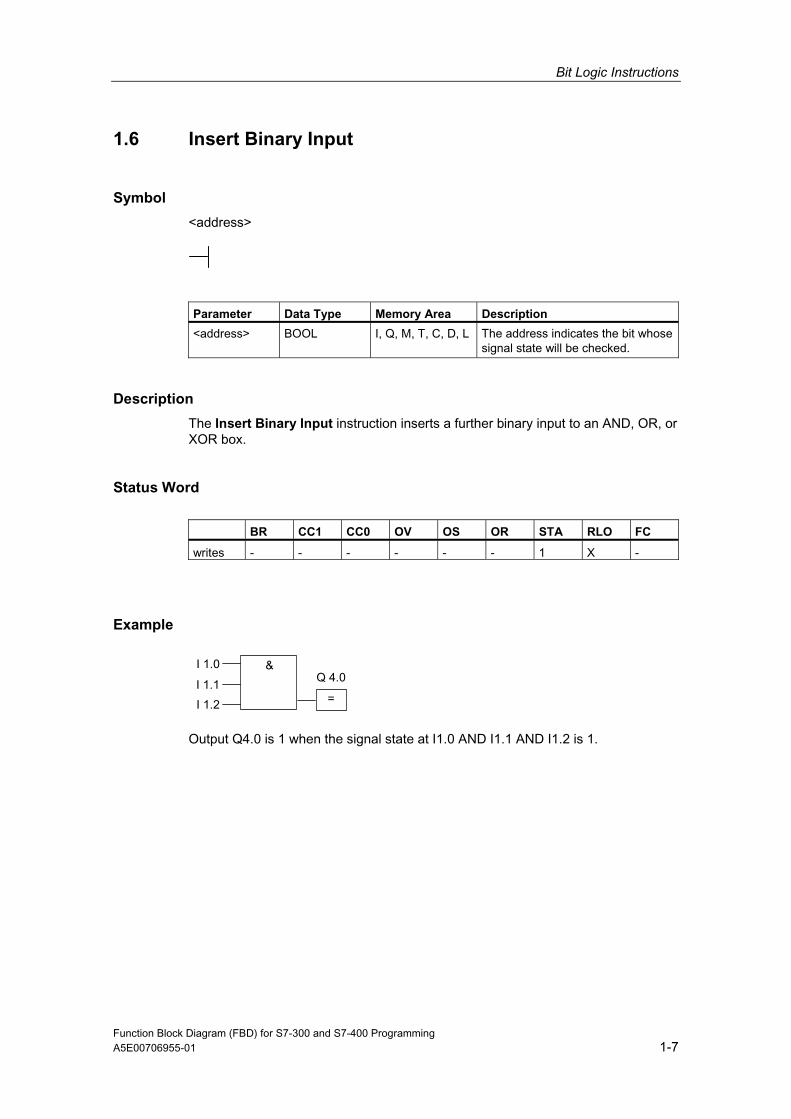
1.6 Insert Binary Input
Symbol
<address>
Parameter Data Type Memory Area Description
<address> BOOL I, Q, M, T, C, D, L The address indicates the bit whosesignal state will be checked.
Description
T er inary put instruction inserts a furthe inary input to an AND, OR, or
BR CC1 CC0 OV OS OR STA RLO FC
he Ins t B In r bXOR box.
Status Word
writes - - - - - - 1 X -
Example
&I 1.0
I 1.1=
Q 4.0
I 1.2
Output Q4.0 is 1 when the signal state at I1.0 AND I1.1 AND I1.2 is 1.
Function Block Diagram (FBD) for S7-300 and S7-400 ProgrammingA5E00706955-01 1-7

Bit Logic Instructions
1.7 Negate Binary Input
Symbol
Description
The Negate Binary Input instruction negates the RLO.
When you negate the result of logic operation, you must remember certain rules:
�� If the result of logic operation at the first input of an AND or OR box is negated, there is no nesting.
�� If the result of logic operation is negated but not at the first input of an OR box,the entire binary logic operation before the input is included in the OR logicoperation.
�� If the result of logic operation is negated but not at the first input of a AND box, the entire binary logic operation before the input is included in the AND logicoperation.
Status Word
BR CC1 CC0 OV OS OR STA RLO FC
writes - - - - - - 1 X -
Example
&I 1.0
I 1.1
>=1&I 1.2
I 1.3Q 4.0
=
&
I 1.4
Output Q4.0 is 1 when:
�� the signal state at I1.0 AND I1.1 is NOT 1
�� AND the signal state at I1.2 AND I1.3 is NOT 1
�� OR the signal state at I1.4 is NOT 1.
Function Block Diagram (FBD) for S7-300 and S7-400 Programming1-8 A5E00706955-01

Bit Logic Instructions
1.8 = : Assign
Symbol
=
<address>
Parameter Data Type Memory Area Description
<address> BOOL I, Q, M, D, L e bit to whichthe signal state of the string of logic operations is assigned.
The address specifies th
Descriptio
of
rations are
/off.
gic
You can create a negated assignment with the Negate Input instruction.
Status Word
A
n
The Assign instruction produces the result of logic operation. The box at the enda logic operation has the signal 1 or 0 according to the following criteria:
�� The output has the signal 1 when the conditions of the logic operation before the output box are satisfied.
�� The output has the signal 0 when the conditions of the logic operation before the output box are not satisfied.
The FBD logic operation assigns the signal state to the output that is addressed bythe instruction (to achieve the same effect, the signal state of the RLO bit couldalso be assigned to the address). If the conditions of the FBD logic opesatisfied, the signal state at the output box is 1. Otherwise the signal state is 0. The Assign instruction is influenced by the Master Control Relay (MCR).
For more detailed information about the functions of the MCR, refer to MCR on
You can only place the Assign box at the right-hand end of the string of looperations. You can, however, use several Assign boxes.
BR CC1 CC0 OV OS OR ST RLO FC
writes - - - - - 0 X - 0
Function Block Diagram (FBD) for S7-300 and S7-400 ProgrammingA5E00706955-01 1-9

Bit Logic Instructions
Example
&I 0.0
I 0.1 >=1Q 4.0
=I 0.2
The signal state at output Q4.0 is 1 when:
�� the signal state is 1 at inputs I0.0 AND I0.1
�� OR I0.2 is 0
Function Block Diagram (FBD) for S7-300 and S7-400 Programming1-10 A5E00706955-01

Bit Logic Instructions
1.9 # : Midline Output
Symbol
#
<address>
ypeParameter Data T Memory Area Description
<address> BOOL I, Q, M, D, *L The address specifies the bwhich the RLO will be assig
it toned.
* You can only use an address in the local data stack if it is declared in the variable declaration table in the TEMP area of a code block (FC, FB, OB).
Descriptio
n intermediate element that buffers the RLO.
R).ff.
You can create a negated Midline Output by negating the input of the Midline Output.
Status Word
A
n
The Midline Output instruction is aMore precisely, this element buffers the bit logic operation of the last branch to beopened before the Midline Output.
The Midline Output instruction is is affected by the Master Control Relay (MCFor more detailed information about how the MCR functions, refer to MCR on/o
BR CC1 CC0 OV OS OR ST RLO FC
writes - - - - - 0 X - 1
Function Block Diagram (FBD) for S7-300 and S7-400 ProgrammingA5E00706955-01 1-11

Bit Logic Instructions
Example
#I 1.0
I 1.1
>=1&I 1.2
I 1.3
M 3.3
#
&
I 1.4
Q 4.0
=
&
M 1.1
#
M 2.2
#
M 0.0
The Midline Outputs buffer the following results of the logic operations:
M0.0 buffers the negated RLO of
&I 1.0
I 1.1
M1.1 saves the negated RLO of
&I 1.2
I 1.3
M2.2 saves the RLO of I1.4
M3.3 saves the negated RLO of the entire bit logic operation
Function Block Diagram (FBD) for S7-300 and S7-400 Programming1-12 A5E00706955-01

Bit Logic Instructions
1.10 R : Reset Output
Symbol
R
<address>
peParameter Data Ty Memory Area Description
<address>
TIMER
COUNTER
I, Q, M, T, C, D, L The address specifies whichbit will be reset.
BOOL
Descriptio
. If the RLO is 1,
The Reset Output instruction is affected by the Master Control Relay (MCR). Formore detailed information about how the MCR functions, refer to MCR on/off.
Status Word
A
n
The Reset Output instruction is only executed when the RLO is 1this instruction resets the specified address to 0. If the RLO is 0, the instructiondoes not affect the specified address which remains unchanged.
BR CC1 CC0 OV OS OR ST RLO FC
writes - - - - - 0 X - 0
Example
&I 0.0
I 0.1 >=1Q 4.0
RI 0.2
The signal state at output Q4.0 is reset to 0 only when:
D I0.1
the RLO of the branch is 0, the signal state at output Q4.0 is unchanged.
�� The signal state is 1 at inputs I0.0 AN
�� OR the signal state at input I0.2 is 0.
If
Function Block Diagram (FBD) for S7-300 and S7-400 ProgrammingA5E00706955-01 1-13

Bit Logic Instructions
1.11 S : Set Output
Symbol
S
<address>
ypeParameter Data T Memory Area Description
<address> BOOL I, Q, M, D, L The address specifies which bit will be set.
Descriptio
s 1. If the RLO is 1, es
The Set Output instruction is affected by the Master Control Relay (MCR). For more detailed information about how the MCR functions, refer to MCR on/off.
Status Word
A
n
The Set Output instruction is only executed when the RLO ithis instruction sets the specified address to 1. If the RLO is 0, the instruction donot affect the specified address which remains unchanged.
BR CC1 CC0 OV OS OR ST RLO FC
writes - - - - - 0 X - 0
Example
&I 0.0
I 0.1 >=1Q 4.0
SI 0.2
The signal state at output Q4.0 is set to 1 only when:
D I0.1
the RLO of the branch is 0, the signal state of Q4.0 is not changed.
�� The signal state is 1 at inputs I0.0 AN
�� OR the signal state at input I0.2 is 0.
If
Function Block Diagram (FBD) for S7-300 and S7-400 Programming1-14 A5E00706955-01

Bit Logic Instructions
1.12 RS : Reset_Set Flip Flop
Symbol
RS
<address>
S Q
R
Parameter Data Type Memory Area ptionDescri
<address> BOOL I, Q, M, D, L The address specifieswhich bit will be set or reset.
S BOOL I, Q, M, D, L, T, C Reset instruction enabled
R BOOL I, Q, M, D, L, T, C Set instruction enabled
Q BOOL I, Q, M, D, L Signal state of <address>
Descriptio
The Reset_Set Flip Flop instruction is affected by the Master Control Relay (MCR). For more detailed information about how the MCR functions, refer to MCR
off.
Status Word
BR CC1 CC0 OV OS OR STA RLO FC
n
The Reset_Set Flip Flop instruction executes instructions such as Set (S) or Reset (R) only when the RLO is 1. An RLO of 0 does not affect these instructions,the address specified in the instruction is not changed.
Reset_Set Flip Flop is reset when the signal state at input R is 1 and the signalstate at input S is 0. If input R is 0 and input S is 1, the flip flop is set. If the RLO atboth inputs is 1, the flip flop is set.
on/
writes - - - - - X X X 1
Function Block Diagram (FBD) for S7-300 and S7-400 ProgrammingA5E00706955-01 1-15

Bit Logic Instructions
Example
&I 0.0I 0.1
RS
M 0.0
S QQ 4.0
=
&I 0.0I 0.1 R
If I0.0 is 1 and I0.1 is 0, the memory bit M0.0 is reset and output Q4.0 is 0. If I0.0 is 0 and I0.1 is 1, the memory bit M0.0 is set and output Q4.0 is 1.
If both signal states are 0, there is no change. If both signal states are 1, the Set instruction dominates due to the order of the instructions. M 0.0 is set and Q4.0 is1.
Function Block Diagram (FBD) for S7-300 and S7-400 Programming1-16 A5E00706955-01

Bit Logic Instructions
1.13 SR : Set_Reset Flip Flop
Symbol
SR
<address>
R Q
S
rameter Data pePa Ty Memory Area Description
<address> h bit willBOOL I, Q, M, D, L The address specifies whicbe set or reset.
S BOOL I, Q, M, D, L, T, C Set instruction enabled
R BOOL I, Q, M, D, L, T, C Reset instruction enabled
Q BOOL I, Q, M, D, L Signal state of <address>
Descriptio
l state
The Set_Reset Flip Flop instruction is affected by the Master Control Relay (MCR). For more detailed information about how the MCR functions, refer to MCR
off.
Status Word
BR CC1 CC0 OV OS OR STA RLO FC
n
The Set_Reset Flip Flop instruction executes Set (S) or Reset (R) instructionsonly when the RLO is 1. An RLO of 0 has no effect on these instructions, the address specified in the instruction remains unchanged.
Set_Reset Flip Flop is set when the signal state at input S is 1 and the signaat input R is 0. If input S is 0 and input R is 1, the flip flop is reset. If the RLO at both inputs is 1 the flip flop is reset.
on/
writes - - - - - X X X 1
Function Block Diagram (FBD) for S7-300 and S7-400 ProgrammingA5E00706955-01 1-17

Bit Logic Instructions
Example
&I 0.0I 0.1
SR
M 0.0
R QQ 4.0
=
&I 0.0I 0.1 S
If I0.0 is 1 and I0.1 is 0, memory bit M0.0 is set and Q4.0 is 1.If I0.0 is 0 and I0.1 is 1, the memory bit M0.0 is reset and Q4.0 is 0.
If both signal states are 0, there is no change. If both signal states are 1, the resetinstruction dominates due to the order of the instructions. M0.0 is reset and Q 4.0 is 0.
Function Block Diagram (FBD) for S7-300 and S7-400 Programming1-18 A5E00706955-01

Bit Logic Instructions
1.14 N : Negative RLO Edge Detection
Symbol
N
<address>
ypeParameter Data T Memory Area Description
<address> BOOL I, Q, M, D, L ecifies whichedge memory bit will store the previous RLO.
The address sp
Descriptio
e RLO prior to the instruction was 0, the RLO is 1 (pulse) after the instruction, in all other cases it is 0. The RLO prior to the instruction is stored in theaddress.
Status Word
A
n
The Negative RLO Edge Detection instruction detects a change from 1 to 0 (falling edge) at the specified address and indicates this by setting the RLO to 1 after the instruction. The current signal state of the RLO is compared with thesignal state of the address (the edge memory bit). If the signal state of the addressis 1 and th
BR CC1 CC0 OV OS OR ST RLO FC
writes - - - - - 0 X X 1
Example
I 1.1
I 1.2 &I 1.3
I 1.4 &
>=1
I 1.0 &&
=
Q 4.0
P
M 0.0
M 1.1
PM 2.2
NM 3.3
N
The edge memory bit M3.3 stores the signal state of the previous RLO.
Function Block Diagram (FBD) for S7-300 and S7-400 ProgrammingA5E00706955-01 1-19

Bit Logic Instructions
1.15 P : Positive RLO Edge Detection
Symbol
P
<address>
ypeParameter Data T Memory Area Description
<address> BOOL I, Q, M, D, L ecifies whichedge memory bit will store the previous RLO.
The address sp
Descriptio
RLO is 1 before the instruction, the RLO will be 1 (pulse) after the instruction, in all other cases the RLO is 0. The RLO prior to the instruction is stored in the address.
Status Word
A
n
The Positive RLO Edge Detection instruction detects a change from 0 to 1 (risingedge) at the specified address and indicates this with an RLO of 1 after the instruction. The current signal state at the RLO is compared with the signal state of the address (the edge memory bit). If the signal state of the address is 0 and the
BR CC1 CC0 OV OS OR ST RLO FC
writes - - - - - 0 X X 1
Example
I 1.1
I 1.2 &I 1.3
I 1.4 &
>=1
I 1.0 &&
=
Q 4.0
P
M 0.0
M 1.1
PM 2.2
NM 3.3
N
The edge memory bit M3.3 stores the signal state of the previous RLO.
Function Block Diagram (FBD) for S7-300 and S7-400 Programming1-20 A5E00706955-01

Bit Logic Instructions
1.16 SAVE : Save RLO to BR Memory
Symbol
SAVE
Descriptio
RLO in the BR bit of the
ation in the next network, the state of
et to the value of the RLO
ordinate block. The CALL instruction in the callingblock resets the first check bit.
Status Word
1 0 S R A LO
n
The Save RLO to BR Memory instruction saves thestatus word. The first check bit FC is not reset.
For this reason, if there is an AND logic operthe BR bit is included in the logic operation.
For the instruction SAVE (LAD, FBD, STL), the following applies and not the recommended use specified in the manual and online help:We do not recommend that you use SAVE and then check the BR bit in the sameblock or in subordinate blocks, because the BR bit can be modified by many instructions occurring inbetween. It is advisable to use the SAVE instruction before exiting a block, since the ENO output (= BR bit) is then sbit and you can then check for errors in the block.
With the Save RLO to BR Memory instruction, the RLO of a network can form part of a logic operation in a sub
BR CC CC OV O O ST R FC
writes - - - - - - - - -
Example
&I 1.2
I 1.3 SAVE
The result of logic operation (RLO) is written to the BR bit.
Function Block Diagram (FBD) for S7-300 and S7-400 ProgrammingA5E00706955-01 1-21

Bit Logic Instructions
1.17 N dre tive te
Symbol
EG : Ad ss Nega Edge De ction
NEG
<address1>
M_BIT Q
Parameter Data Type Memory Area Description
<address1> BOOL I, Q, M, D, L Signal to be checked for a negative (falling) edge change.
M_BIT BOOL Q, M, D The M_BIT address specifies the edge memory bit in which theprevious signal state of NEG isstored. Only use the process input image I memory area for the M_BIT when no input moduleis already using this address.
Q BOOL I, Q, M, D, L One-shot output.
Description
The Address Negative Edge Detection instruction compares the signal state of<address1> with the signal state of the previous check that is stored in the M_BITparameter. If a change from 1 to 0 occurred, output Q has the value 1, in all other situations it has the value 0.
Status Word
BR CC1 CC0 OV OS OR STA RLO FC
writes - - - - - 0 1 X 1
Example
NEG
I 0.3
M_BIT Q&
I 0.4Q 4.0
=
Output Q4.0 is 1 when:
�� there is a falling edge at input I0.3
� AND the signal state at input I0.4 is 1.
M 0.0
�
Function Block Diagram (FBD) for S7-300 and S7-400 Programming1-22 A5E00706955-01

Bit Logic Instructions
1.18 P dre ositive tec
Symbol
OS : Ad ss P Edge De tion
POS
<address1>
M_BIT Q
Parameter Data Type Memory Area Description
<address1> BOOL I, Q, M, D, L Signal to be checked for a positive (rising) edge.
M_BIT BOOL Q, M, D The M_BIT address specifies theedge memory bit used to storethe previous signal state of POS.You should only use the processimage input area I for the M_BITwhen no input module is alreadyusing this address.
Q BOOL I, Q, M, D, L One-shot output.
Description
The Address Positive Edge Detection instruction compares the signal state of<address1> with the signal state of the previous signal check that is stored in theparameter M_BIT. If there has been a change from 0 to 1, output Q has the value1, in all other cases it has the value 0.
Status Word
CC0 OV OS OR STA RLO FCBR CC1
writes - - - - - 0 1 X 1
Example
POS
I 0.3
M_BIT Q&
I 0.4Q 4.0
=
M 0.0
Output Q4.0 is 1 when:
there is a rising edge at input I0.3
AND the signal state is 1 at input I0.4.
Function Block Diagram (FBD) for S7-300 and S7-400 ProgrammingA5E00706955-01 1-23

Function Block Diagram (FBD) for S7-300 and S7-400 Programming A5E00706955-01 12-1
12 Status Bit Instructions
12.1 Overview of Status Bit Instructions
Description The status bit instructions are bit logic instructions that work with the bits of the status word (see CPU Registers). Each of these instructions reacts to one of the following conditions that is indicated by one or more bits of the status word:
� The binary result bit (BR) is set (has a signal state of 1).
� The result of a math function is relative to 0 in one of the following ways: == 0, <> 0, > 0, < 0, >= 0, <= 0.
� The result of a math function is unordered (UO).
� A math function produced an overflow (OV) or a or a stored overflow (OS).
When a status bit instruction is connected in series, it combines the result of its signal state check with the previous result of logic operation according to the And truth table. When a status bit instruction is connected in parallel, it combines its result with the previous RLO according to the Or truth table.
Status word The status word is a Register in the memory of your CPU that contains bits that you can reference in the address of bit and word logic instructions. Structure of the status word:
You can evaluate the bits in the status word
� by Integer Math Functions
� by Floating-Point Functions
BR CC1 CC0 OV OS OR STA RLO /FC28 27 26 25 24 23 2 2 2 1 2 0 ...29 2 15 ...

Status Bit Instructions
12.2 OV : Exception Bit Overflow
Symbol
OV
Description
You can us the Exception it Ov flow i ructio dete an ov low (O ) ine last math function. If, after the system executes a math function, the result is
outside the permitted negative range or outside the permitted positive range, theOV bit in the status word (see also CPU Registers) is set. The instruction checksthe signal state of this bit. This bit is reset if the math functions were free of errors
Status Word
CC1 CC0 OV OS OR STA RLO FC
e B er nst n to ct erf Vth
BR
writes - - - - - X X X 1
Example
Network 1
SUB_IEN
ENOIN2
OUTIN1
IW2
IW0
I 0.0
MW10
Network 2
&
M 3.3
>=1
I 0.1
I 0.2
I 0.3
Function Block Diagram (FBD) for S7-300 and S7-400 Programming12-2 A5E00706955-01

Status Bit Instructions
Network 3
OV
S
Q 4.0
If the signal state at input I0.0 is 1, the SUB_I box is activated. If the result of the math function input word IW0 minus input word IW2 is outside the permitted rangefor an integer, the OV bit in the status word is set. The result of a signal state check
signal state of both EN andNO is 0. If the signal state of EN is 1 (activated) and the result of the math
function is out of range, the signal state of ENO is 0.
at OV is 1. Output Q4.0 is set if the check at OV is 1 and the RLO of network 2 is 1(if the RLO prior to output Q4.0 is 1).
If the signal state of input I0.0 is 0 (not activated), theE
Function Block Diagram (FBD) for S7-300 and S7-400 ProgrammingA5E00706955-01 12-3

Status Bit Instructions
12.3 OS : Exception Bit Overflow Stored
Symbol
OS
Description
In an AND operation, this instruction combines the result of its check with theprevious result of logic operation according to the AND truth table. In an OR operation, the OR truth table is used.
You can use the Exception Bit Overflow Stored instruction to recognize a previous overflow (overflow stored, OS) in a math function. If, after the systemexecutes a math function, the result is outside the permitted negative range oroutside the permitted positive range, the OS bit in the status word (see also CPURegisters) is set. The instruction checks the signal state of this bit. Unlike the OV(overflow) bit, the OS bit remains set even if later math functions were executedfree of errors (see also OV : Exception Bit Overflow ).
Status Word
BR CC1 CC0 OV OS OR STA RLO FC
writes X- - - - - X X 1
Example
Network 1
MUL_IEN
ENOIN2
OUTIN1
IW2
I 0.0
MD8
Network 2
IW0
ADD_IEN
ENOIN2
OUTIN1
IW2
IW0
I 0.1
MW12
Function Block Diagram (FBD) for S7-300 and S7-400 Programming12-4 A5E00706955-01

Status Bit Instructions
Network 3
OS
S
Q 4.0
If the signal state at input I0.0 is 1, the MUL_I box is activated. If the signal state at input I0.1 is 1, the ADD_I box is activated. If the result of one of the math functions
.
), the signal state of he
), the signal state of oth EN and ENO is 0. If the signal state of EN is 1 (activated) and the result of the
math function is out of range, the signal state of ENO is 0.
is outside the permissible range for an integer, the OS bit in the status word is set
The result of a signal state check at OS is 1 and output Q4.0 is set.
Network 1: if the signal state of input I0.0 is 0 (not activatedboth EN and ENO is 0. If the signal state of EN is 1 (activated) and the result of tmath function is out of range, the signal state of ENO is 0.
Network 2: if the signal state of input I0.1 is 0 (not activatedb
Function Block Diagram (FBD) for S7-300 and S7-400 ProgrammingA5E00706955-01 12-5

Status Bit Instructions
12.4 UO : Exception Bit Unordered
Symbol
UO
Description
You can use the Exception Bit Unordered instruction to check whether or not the result of a floating-point math function is unordered (in other words, whether one of the values in the math function is not a valid floating-point number). The conditioncode bits of the status word (CC 1 and CC 0, see CPU Registers) are evaluated. If the result of the math function is unordered (UO) the signal state check produces a result of 1. If the combination in CC 1 and CC 0 does not indicate unordered, theresult of the signal state check is 0.
Status Word
OV OS OR BR CC1 CC0 STA RLO FC
writes - - - - - X X X 1
Example
Network 1
DIV_REN
ENOIN2
OUTIN1
ID4Q 4.1
S
MD10
Network 2
ID0
I 0.0
UO
S
Q 4.0
If the signal state at input I0.0 is 1, the DIV_R box is activated. If the value of eithert
hile the instruction is being executed, the signal state of ENO is 0.
Output Q4.0 is set if the function DIV_R is executed, but one of the values in themath function is not a valid floating-point number. If the signal state of input I0.0 is 0 (not activated), the signal state of both EN and ENO is 0.
input double word ID0 or ID4 is not a valid floating-point number, the floating-poinmath function is unordered.If the signal state of EN is 1 (activated) and an error occurs w
Function Block Diagram (FBD) for S7-300 and S7-400 Programming12-6 A5E00706955-01

Status Bit Instructions
12.5 BR : Exception Bit BR Memory
Symbol
BIEBR
English German
Descriptio
You can use the Exception Bit BR Memory instruction to check the signal state of the BR bit (Binary Result) of the status word (see CPU Registers).
Status Word
BR CC1 CC0 OV OS OR STA RLO FC
n
writes - - - - - X X X 1
Example
& Q 4.0
>=1I 0.0
I 0.2
BR S
OI0.2 is 0, and, in addition to
utput Q4.0 is set if the signal state at input I0.0 is 1 OR the signal state at input this RLO, the signal state of the BR bit is 1.
Function Block Diagram (FBD) for S7-300 and S7-400 ProgrammingA5E00706955-01 12-7

Status Bit Instructions
12.6 <> 0 : Result Bits
Symbols
== 0 The Result Bit instruction for equal to 0 determines whether or not the result of a math instruction is equal to 0.
<> 0 The Result Bit instruction for not equal to 0 determines whether or not the result of a math instruction is not equal to 0.
> 0 The Result Bit instruction for greater than 0 determines whether or not the result of a math instruction is greater than 0
< 0 The Result Bit instruction for less than 0 determines whether or not the result of a math instruction is less than 0.
>= 0 The Result Bit instruction for greater than or equal to 0 determines whether or not the result of a math instruction greater than or equal to 0.
<= 0 The Result Bit instruction for less than or equal to 0 determines whether or not the result of a math instruction is less than or equal to 0.
Description
You can use the Result Bit instructions to determine the relationship of the result of a math function to zero, in other words, whether the result is ==0, <>0; >0, <0, >=0 OR <=0. The condition code bits of the status word (CC 1 and CC 0, see CPURegisters) are evaluated. If the comparison condition indicated in the address isfulfilled, the result of this signal state check is 1.
In an AND operation, this instruction combines the result of its check with theprevious result of logic operation (RLO) according to the AND truth table. In an OR operation, this instruction combines the result of its check with the previous RLOaccording to the OR truth table.
FC
Status Word
BR CC1 CC0 OV OS OR STA RLO
writes - - - - - X X X 1
Function Block Diagram (FBD) for S7-300 and S7-400 Programming12-8 A5E00706955-01

Status Bit Instructions
Example
2)SUB_I
IN2
OUT
IW2
MW10IN1IW0
EN
ENO
I 0.0
Q 4.0
S
&
<=0
1)SUB_I
IN2
OUT MW10IN1
EN
ENO
0.0
IW2
IW0
I
Q 4.0
S>0
&
If the signal state at input I0.0 is 1, the SUB_I box is activated. If the value of inputword IW0 is greater than the value of input word IW2, the result of the math function IW0 - IW2 is greater than 0. If the signal state of EN is 1 (activated) and an error occurs while the instruction is being executed, the signal state of ENO is 0.
1. Output Q4.0 is set if the function is executed correctly and the result is less thanor equal to 0. If the signal state of input I0.0 is 0 (not activated), the signal state of both EN and ENO is 0.
2. Output Q4.0 is set if the function is executed correctly and the result is less thanor equal to 0. If the signal state of input I0.0 is 0 (not activated), the signal state of both EN and ENO is 0.
Function Block Diagram (FBD) for S7-300 and S7-400 ProgrammingA5E00706955-01 12-9

4.PLC Programing Using BIT Operations Write down the program and experiment to evaluate the results.
1) Reactor Tank
2) Motor Control: Direct On‐Line Start