1 a design approach for radiation-hard digital electronics rajesh garg nikhil jayakumar sunil p...
Post on 18-Dec-2015
214 views
TRANSCRIPT

1
A Design Approach for A Design Approach for Radiation-hard Digital Radiation-hard Digital
ElectronicsElectronicsRajesh GargRajesh Garg
Nikhil JayakumarNikhil JayakumarSunil P KhatriSunil P Khatri
Gwan ChoiGwan Choi
Department of Electrical and Computer Engineering,Department of Electrical and Computer Engineering,
Texas A&M University, College Station, TX-77840Texas A&M University, College Station, TX-77840

2
OutlineOutline
IntroductionIntroduction ObjectiveObjective Previous ApproachesPrevious Approaches Our ApproachOur Approach ResultsResults ConclusionsConclusions

3
IntroductionIntroduction
There has been significant interest in the radiation There has been significant interest in the radiation immunity of electronic circuitsimmunity of electronic circuits Historically mainly used for space and military electronicsHistorically mainly used for space and military electronics Higher levels of radiation in space and combat environmentsHigher levels of radiation in space and combat environments
More recently, terrestrial electronics are also More recently, terrestrial electronics are also becoming vulnerablebecoming vulnerable Shrinking feature size and supply voltagesShrinking feature size and supply voltages Reduced capacitances means less charge is required to flip Reduced capacitances means less charge is required to flip
node voltagenode voltage This has led to a renewed interest in radiation tolerant circuit This has led to a renewed interest in radiation tolerant circuit
designdesign

4
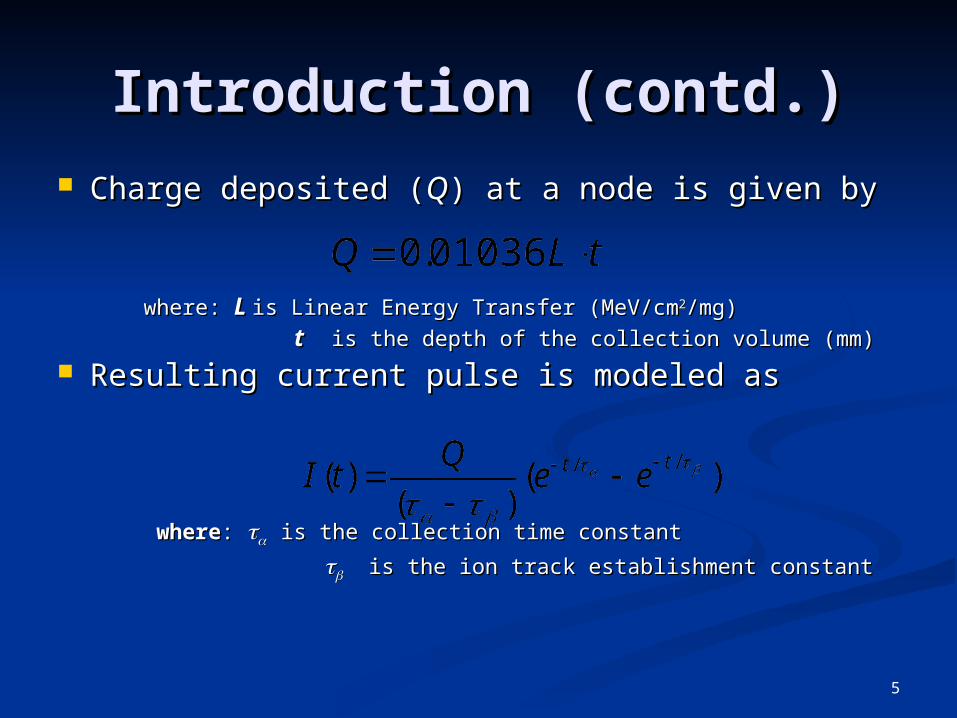
Introduction (contd.)Introduction (contd.)
Effects of radiation particle strikeEffects of radiation particle strike Neutron, proton and heavy cosmic ionsNeutron, proton and heavy cosmic ions Ions strike diffusion regionsIons strike diffusion regions Deposit chargeDeposit charge Results in a voltage spikeResults in a voltage spike
What is Single Event Upset (SEU)?What is Single Event Upset (SEU)? Interaction of a radiation particle with VLSI circuits can Interaction of a radiation particle with VLSI circuits can
produce a charge deposition in critical regions of the produce a charge deposition in critical regions of the circuit, leading to a bit reversal error, or circuit, leading to a bit reversal error, or single event upsetsingle event upset..
5
Introduction (contd.)Introduction (contd.)
Charge depositedCharge deposited ( (QQ) ) at a node is given byat a node is given by
where:where: LL is Linear Energy Transfer (MeV/cmis Linear Energy Transfer (MeV/cm22/mg)/mg)
tt is the depth of the collection volume (mm)is the depth of the collection volume (mm)
Resulting current pulse is modeled asResulting current pulse is modeled as
wherewhere:: is the collection time constantis the collection time constant
is the ion track establishment constantis the ion track establishment constant

6
ObjectivesObjectives
Radiation particles cause SEURadiation particles cause SEU Terrestrial electronics are also susceptible to Terrestrial electronics are also susceptible to
SEUSEU Therefore, need circuit level protection against Therefore, need circuit level protection against
SEU even for consumer electronicsSEU even for consumer electronics To make circuit radiation tolerantTo make circuit radiation tolerant Delay and area overhead should be minimizedDelay and area overhead should be minimized

7
Previous ApproachesPrevious Approaches
Transistor sizing is done to improve the radiation Transistor sizing is done to improve the radiation tolerance of the design (Zhou et. al)tolerance of the design (Zhou et. al) Ensure that capacitance of any node is sufficient to make Ensure that capacitance of any node is sufficient to make
the circuit radiation tolerant.the circuit radiation tolerant.
SEU event is detected using built in current sensor SEU event is detected using built in current sensor (BICS) (Gill et. al)(BICS) (Gill et. al)
Triple modulo redundancy based approach Triple modulo redundancy based approach (Neumann et. al)(Neumann et. al)
Error correction codes (Gambles et. al)Error correction codes (Gambles et. al) More detailed references can be found in the paperMore detailed references can be found in the paper

8
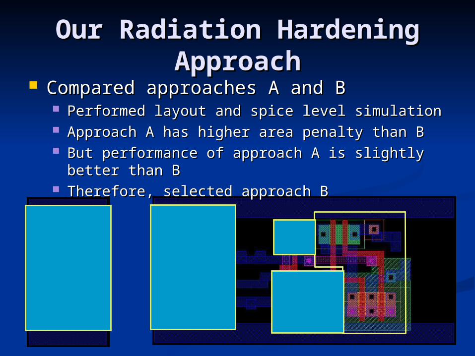
Our Radiation Hardening Our Radiation Hardening ApproachApproach
Part 1: Gate Level SEU protectionPart 1: Gate Level SEU protection Approach A: PN Junction Diode based SEU Clamping Approach A: PN Junction Diode based SEU Clamping
CircuitsCircuits Approach B: Diode-connected Device based SEU Approach B: Diode-connected Device based SEU
Clamping CircuitsClamping Circuits
Part 2: Logic Block Level ProtectionPart 2: Logic Block Level Protection Radiation hardening for all gatesRadiation hardening for all gates Fixed depth protectionFixed depth protection Variable depth protectionVariable depth protection

9
Our Radiation Hardening Our Radiation Hardening ApproachApproach
Approach A - PN Junction Diode based SEU Approach A - PN Junction Diode based SEU Clamping CircuitsClamping Circuits
G
GP
in
1V
0V
1.4V
-0.4V
outP
out
D2 D1
Higher VT
device
Radiation Strike
V (out)
time0
0.2
0.4
0.6
0.8
V (outP)
time0
0.2
0.4
0.6
0.8
-0.4
Shadow Gate

10
Our Radiation Hardening Our Radiation Hardening ApproachApproach
Approach B - Diode-connected Device based Approach B - Diode-connected Device based SEU Clamping CircuitsSEU Clamping Circuits
G
GP
in
1V
0V
1.4V
-0.4V
outP
out
D2 D1
Higher VT
device
Radiation Strike
V (out)
time0
0.2
0.4
0.6
0.8
V (outP)
time0
0.2
0.4
0.6
0.8
-0.4
Ids
11
Our Radiation Hardening Our Radiation Hardening ApproachApproach
Compared approaches A and BCompared approaches A and B Performed layout and spice level simulation Performed layout and spice level simulation Approach A has higher area penalty than BApproach A has higher area penalty than B But performance of approach A is slightly better than BBut performance of approach A is slightly better than B Therefore, selected approach BTherefore, selected approach B

12
Simulating a Radiation StrikeSimulating a Radiation Strike
Circuit simulation is performed in SPICECircuit simulation is performed in SPICE 65nm BPTM model card is used65nm BPTM model card is used
VVDD DD = 1V= 1V
VVTTNN = = | V| VTTPP| = | = 0.22V0.22V
The radiation strike was modeled as current The radiation strike was modeled as current sourcesource As commonly done in this field (Zhou et. al)As commonly done in this field (Zhou et. al) Varied the value ofVaried the value of QQ andand
is chosen to be 5ps (Gill et. al)is chosen to be 5ps (Gill et. al)

13
Simulating a Radiation StrikeSimulating a Radiation Strike
Injected Current as a function ofInjected Current as a function of QQ andand

14
Protection Performance - Protection Performance - ExampleExample
Radiation Radiation strike at strike at output nodeoutput node.. Q Q = 4 fC= 4 fC 10ps10ps
Approach B Approach B is usedis used

15
Block Level Radiation HardeningBlock Level Radiation Hardening
Individual gate protectionIndividual gate protection Approach B is selectedApproach B is selected Area overhead is more than 100%Area overhead is more than 100%
But our goal is to protect the entire logic circuitBut our goal is to protect the entire logic circuit We call it as We call it as block level protectionblock level protection
To understand block level protectionTo understand block level protection Critical depth of a gateCritical depth of a gate

16
Critical Depth of a GateCritical Depth of a Gate
Consider 2 input AND gateConsider 2 input AND gate Computed for each hardened cellComputed for each hardened cell
11
1 1 1
Radiation Strike
Produces glitch
Magnitude of glitch reduces
Glitch magnitude is
tolerableCritical Depth =3

17
Critical Depth of a GateCritical Depth of a Gate
Spice simulations were Spice simulations were performed usingperformed using
Q Q = 5 fC, = 5 fC, 10ps, 10ps, 5ps 5ps
Tolerable glitch magnitude Tolerable glitch magnitude isis 0.35*V 0.35*VDDDD
Gate NameGate Name Critical Critical Depth (Depth (ΔΔ))
inv2AAinv2AA 55
inv4AAinv4AA 11
nand2AAnand2AA 11
nand3AAnand3AA 11
nand4AAnand4AA 11
nor2AAnor2AA 11
nor3AAnor3AA 11
nor4AAnor4AA 11
and2AAand2AA 22
and3AAand3AA 11
and4AAand4AA 11
or2AAor2AA 11
or3AAor3AA 11
or4AAor4AA 11

18
Block Level Radiation HardeningBlock Level Radiation Hardening
Simple approach – radiation hardening for Simple approach – radiation hardening for all gatesall gates
Very inefficient approachVery inefficient approach Large delay and area overheadLarge delay and area overhead
Primary
Inputs
Primary
Outputs

19
Block Level Radiation HardeningBlock Level Radiation Hardening
Better approach – Fixed depth protectionBetter approach – Fixed depth protection LetLet Δ Δmaxmax= max= maxCC(Δ((Δ(CC))))
AssumeAssume Δ Δmaxmax = 2 = 2 thenthen
Primary
Inputs
Primary
Outputs
Radiation Strike
Radiation Strike

20
Block Level Radiation HardeningBlock Level Radiation Hardening
Further improvement – Variable depth Further improvement – Variable depth protectionprotection
Primary
Inputs
Primary
Outputs

21
Variable Depth ProtectionVariable Depth Protection LetLet ΔΔ(INV2AA) = 4, (INV2AA) = 4, ΔΔ(NAND2AA) = 1 (NAND2AA) = 1 andand
ΔΔ(AND2AA) = 2(AND2AA) = 2 Maximum depth of protection required is 4Maximum depth of protection required is 4
More details of the algorithm can be found in the More details of the algorithm can be found in the paperpaper
Primary
Inputs
Primary
Outputs
1
2
3
4
5
6
7
8
9
10

22
ExperimentsExperiments
Used our approach on some benchmark circuits.Used our approach on some benchmark circuits. Used SIS for synthesis and technology mapping.Used SIS for synthesis and technology mapping. Circuits were mapped for both delay and area.Circuits were mapped for both delay and area. Used the “Used the “sense”sense” package in SIS to find circuit package in SIS to find circuit
delays.delays. sensesense reports the largest sensitizeable delay. reports the largest sensitizeable delay.
To get accurate area estimates, circuits were To get accurate area estimates, circuits were placed and routed using SEDSM from Cadence.placed and routed using SEDSM from Cadence. QPLACE for placement, WROUTE for routingQPLACE for placement, WROUTE for routing

23
Delay Characteristics of the CellsDelay Characteristics of the Cells
Cell Regular (ps) Hardened (ps) % OvhCriticalDepth
inv2AA 24.614 28.012 3.4 5
inv4AA 23.914 23.576 -0.34 1
nand2AA 31.416 34.993 3.58 1
nand3AA 44.92 48.39 3.47 1
nand4AA 62.436 66.259 3.82 1
nor2AA 45.617 49.902 4.29 1
nor3AA 77.151 82.786 5.64 1
nor4AA 92.80364 95.38472 2.58 1
and2AA 57.476 61.911 4.44 2
and3AA 76.902 82.722 5.82 1
and4AA 98.752 107.329 8.58 1
or2AA 71.161 74.678 3.52 1
or3AA 112.871 116.304 3.43 1
or4AA 125.165 128.543 3.38 1
AVG 3.97

24
Block Level Delay ResultsBlock Level Delay Results Delay overhead Delay overhead
primarily due to primarily due to increased increased capacitive load capacitive load from hardended from hardended cells.cells.
Delay Overhead
Area Mapped Delay Mapped
Ckt. Regular Hardened % Ovh Regular Hardened %Ovh
alu2 1057.99 1068.913 1.03 959.113 976.987 1.86
alu4 1318.652 1357.851 2.97 1247.762 1259.695 0.96
C1355 887.619 920.186 3.67 711.149 720.345 1.29
C1908 1301.522 1349.072 3.65 1085.28 1093.79 0.78
C3540 1546.819 1625.472 5.08 1414.443 1424.782 0.73
C499 887.619 920.186 3.67 711.149 720.345 1.29
C880 1489.53 1643.51 10.34 1405.322 1554.847 10.64
dalu 1167.817 1252.608 7.26 1056.534 1077.134 1.95
frg2 825.852 912.605 10.5 792.849 836.477 5.5
i2 451.879 463.949 2.67 363.611 382.298 5.14
i3 172.865 184.777 6.89 172.865 184.777 6.89
C7552 2012.924 2100.094 4.33 2005.371 2070.491 3.25
i10 1997.302 2253.81 12.84 1931.211 2002.74 3.7
AVG 5.76 3.38

25
Block Level Area ResultsBlock Level Area Results Area overhead is Area overhead is
larger for circuits larger for circuits mapped for mapped for minimum areaminimum area
Area overhead is Area overhead is also large for circuits also large for circuits with smaller logic with smaller logic depth (such as frg2depth (such as frg2))
Area Overhead
Area Mapped Delay Mapped
Ckt. Regular Hardened % Ovh Regular Hardened %Ovh
alu2 1045.88 1728.9 65.31 1439.44 1728.9 20.11
alu4 2019.6 2830.24 40.14 2470.09 3343.15 35.35
C1355 1592.01 2252.45 41.48 1728.9 2279.11 31.82
C1908 1569.74 2252.45 43.49 1799.46 2279.11 26.66
C3540 3136 4763.76 51.91 4022.1 5077.99 26.25
C499 1569.74 2265.76 44.34 1728.9 2279.11 31.82
C880 1045.88 1883.56 80.09 1397.26 2252.45 61.2
dalu 2470.09 3540.25 43.32 3310.85 3986.66 20.41
frg2 1994.52 4725.19 136.91 2611.21 4057.69 55.4
i2 686.61 745.29 8.55 872.61 948.64 8.71
i3 495.51 586.61 18.39 495.51 566.44 14.32
C7552 7032.5 12638.26 79.71 7953.07 9576.58 20.41
i10 6845.9 9604 40.28 7705.32 11291.18 46.53
AVG 53.37 30.68

26
Conclusions, Future WorkConclusions, Future Work We have presented a We have presented a novel circuit design approachnovel circuit design approach for for
radiation hardened circuit design.radiation hardened circuit design.
We use We use shadow gatesshadow gates and protecting diode-connected and protecting diode-connected devices to protect the primary gate from a radiation devices to protect the primary gate from a radiation strike.strike.
We presented techniques to replace fewer gates to help We presented techniques to replace fewer gates to help minimize the area and delay penalties.minimize the area and delay penalties. Only Only 30% area penalty30% area penalty and and 4% delay penalty4% delay penalty on average for on average for
circuits mapped for minimum delay.circuits mapped for minimum delay.
In the future we hope to be able to incorporate radiation In the future we hope to be able to incorporate radiation hardening in the technology mapping step itself.hardening in the technology mapping step itself.

27
Thank You!!Thank You!!

28
Our Radiation Hardening Our Radiation Hardening ApproachApproach
Radiation strike at the output of the shadow gateRadiation strike at the output of the shadow gate Output is protected upto 0.4+0.6+0.35 V glitchOutput is protected upto 0.4+0.6+0.35 V glitch
G
GP
in
1V
0V
1.4V
-0.4V
outP
out
D2 D1
Radiation Strike
V (out)
time0
0.2
0.4
0.6
0.8
V (outP)
time0
0.2
0.4
0.6
0.8
-0.4
Shadow Gate

29
Our Radiation Hardening Our Radiation Hardening ApproachApproach
Radiation strike at the output of the shadow gateRadiation strike at the output of the shadow gate
G
GP
in
1V
0V
1.4V
-0.4V
outP
out
D2 D1
Radiation Strike
V (out)
time
00.2
0.4
0.6
0.8
V (outP)
time
00.2
0.4
0.6
0.8
-0.4
Shadow Gate