02 operational amplifier
TRANSCRIPT
8/12/2019 02 Operational Amplifier
http://slidepdf.com/reader/full/02-operational-amplifier 1/12
Operational Amplifiers
2OPERATIONAL AMPLIFIER
Introduction
Operational Amplifier is popularly known as “Op-Amp” It has very high gain, high inputimpedance and low output impedance. It is an integrated circuit (I! amplifier consisting
of many transistors, resistors and a few diodes etc. within it. It has ac"uired its namefrom the fact that it performs many mathematical operations such as differentiation,integration, summation etc. in addition to amplification. It finds use in audio amplifiers,#$ amplifiers, voltage regulators and some special consumer Is for radio and %&receivers. %he advantages of O'-Amp. are small sie, high relia)ility reduced cost etc.
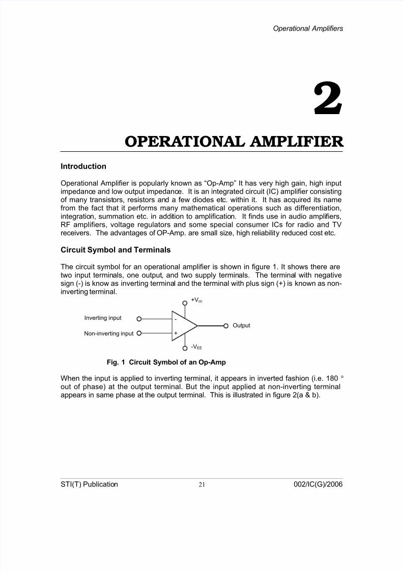
Circuit Symbol and Terminals
%he circuit sym)ol for an operational amplifier is shown in figure *. It shows there aretwo input terminals, one output, and two supply terminals. %he terminal with negativesign (-! is know as inverting terminal and the terminal with plus sign (+! is known as non-inverting terminal.
Fig. 1 Circuit Symbol of an Op-Amp
+&cc
-&
+
-
Output
Inverting input
on-inverting input
hen the input is applied to inverting terminal, it appears in inverted fashion (i.e. */0 o
out of phase! at the output terminal. 1ut the input applied at non-inverting terminalappears in same phase at the output terminal. %his is illustrated in figure 2(a 3 )!.
4%I(%! 'u)lication 21 0025I(6!52007

8/12/2019 02 Operational Amplifier
http://slidepdf.com/reader/full/02-operational-amplifier 2/12
Induction Course (General)
(a! Input fed to inverting terminal
+&cc
-&,,
+
-OutputInput
()! Input fed to non-inverting terminal
+&cc
-&
-
+OutputInput
Fig. 2 Output-Input relation
Characteristics of an Ideal Op-Amp
%he ideal Op-Amp has the following characteristics 8
*. &oltage 6ain 9 ∞2. Input Impedance 9 ∞:. Output Impedance 9 0;. 1andwidth 9 ∞<. 'erfect )alance i.e. ero output voltage
hen )oth the inputs are e"ual
Characteristics of an ractical Op-Amp
A practical Operational Amplifier cannot have characteristics as descri)ed a)ove for anideal Op-Amp. %he Op-Amp I-=;* which is used in many applications has the followingcharacteristics.
*. &oltage gain 9 <0000 (>inimum!9 200000 (%ypical!
2. Input Impedance 9 0.: >Ω (minimum!
9 2 >Ω (typical!:. Output Impedance 9 =< Ω (typical!
;. o perfect )alance 9 there is input offset voltagefor ero output voltage
<. ?imited 1andwidth
4%I(%! 'u)lication 22 0025I(6!52007
8/12/2019 02 Operational Amplifier
http://slidepdf.com/reader/full/02-operational-amplifier 3/12
Operational Amplifiers
arameters of Op-Amp
very Op-Amp has a ma@imum input voltage range and a ma@imum output voltagerange. ue to )ias voltage change, supply voltage variation and A ripple on thesupply voltage, unwanted output can occur. %here is a limit on how fast an Op-Ampoutput can )e made to change and also there is limit on the highest signal fre"uency that
may )e employed. hat follows here is the discussion on various parameter of Op-Amp
Input !oltage "ange
%he ma@imum positive-going and negative going input voltage that may )e applied to anOp-Amp is termed as input voltage range. %he input voltage range for =;* Op-Amp is +*:& (typical! when the supply voltage is +*<&.
Output #oltage "ange
$or most Op-Amp the ma@imum output voltage swing is appro@imately e"ual to *& lessthan the supply voltage. %he output voltage swing for =;* Op-Amp is +*;& when the
supply voltage is +*<& and load resistance #? ≥*0BΩ.
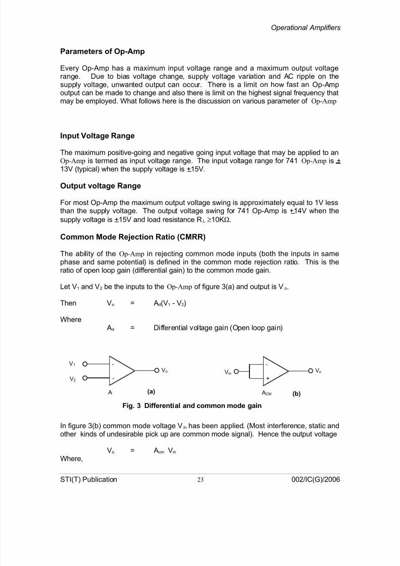
Common $ode "e%ection "atio &C$""'
%he a)ility of the Op-Amp in reCecting common mode inputs ()oth the inputs in samephase and same potential! is defined in the common mode reCection ratio. %his is theratio of open loop gain (differential gain! to the common mode gain.
?et &* and &2 )e the inputs to the Op-Amp of figure :(a! and output is &o.
%hen &o 9 Ad(&* - &2!
here Ad 9 ifferential voltage gain (Open loop gain!
Fig. ( )ifferential and common mode gain
&*
A
-
-
&2
&o
A>
+
-
&in &o
&a'
&b'
In figure :()! common mode voltage &in has )een applied. (>ost interference, static andother kinds of undesira)le pick up are common mode signal!. Dence the output voltage
&o 9 Acm &in
here,
4%I(%! 'u)lication 23 0025I(6!52007
8/12/2019 02 Operational Amplifier
http://slidepdf.com/reader/full/02-operational-amplifier 4/12
Induction Course (General)
Acm 9 ommon mode gain.
%hen the common mode reCection ratio will )e
cmA
dA>## =
%he typical value of >## (in d1! for =;* Op-Amp is E0 d1.
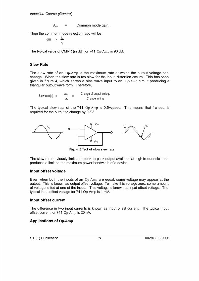
Sle* "ate
%he slew rate of an Op-Amp is the ma@imum rate at which the output voltage canchange. hen the slew rate is too slow for the input, distortion occurs. %his has )eengiven in figure ;, which shows a sine wave input to an Op-Amp circuit producing atriangular output wave form. %herefore,
timeinhange
voltageoutputof hange
t
&!s(rate4lew o
=
∆
∆=
%he typical slew rate of the =;* Op-Amp is 0.<&5µsec. %his means that *µ sec. is
re"uired for the output to change )y 0.<&.
Fig. + ,ffect of slo* sle* rate
+&cc
-&,,
-
+&i &i
&o
%he slew rate o)viously limits the peak-to-peak output availa)le at high fre"uencies andproduces a limit on the ma@imum power )andwidth of a device.
Input offset #oltage
ven when )oth the inputs of an Op-Amp are e"ual, some voltage may appear at theoutput. %his is known as output offset voltage. %o make this voltage ero, some amountof voltage is fed at one of the inputs. %his voltage is known as input offset voltage. %hetypical input offset voltage for =;* Op-Amp is * m&.
Input offset current
%he difference in two input currents is known as input offset current. %he typical inputoffset current for =;* Op-Amp is 20 nA.
Applications of Op-Amp
4%I(%! 'u)lication 24 0025I(6!52007
8/12/2019 02 Operational Amplifier
http://slidepdf.com/reader/full/02-operational-amplifier 5/12
Operational Amplifiers
4ince the Op-Amp has very high gain, it is not suita)le for use in open loop condition inmany cases. ith suita)le feed)ack it is used as voltage follower, Inverting Amplifier.on inverting Amplifier, ifferentiator, Integrator, 4umming Amplifier, 'recision #ectifier,
Active $ilter, ?og Amplifier, 4ample and hold circuit, 'recision 'eak etector,omparator, etc. 4ome of these are discussed )elow.
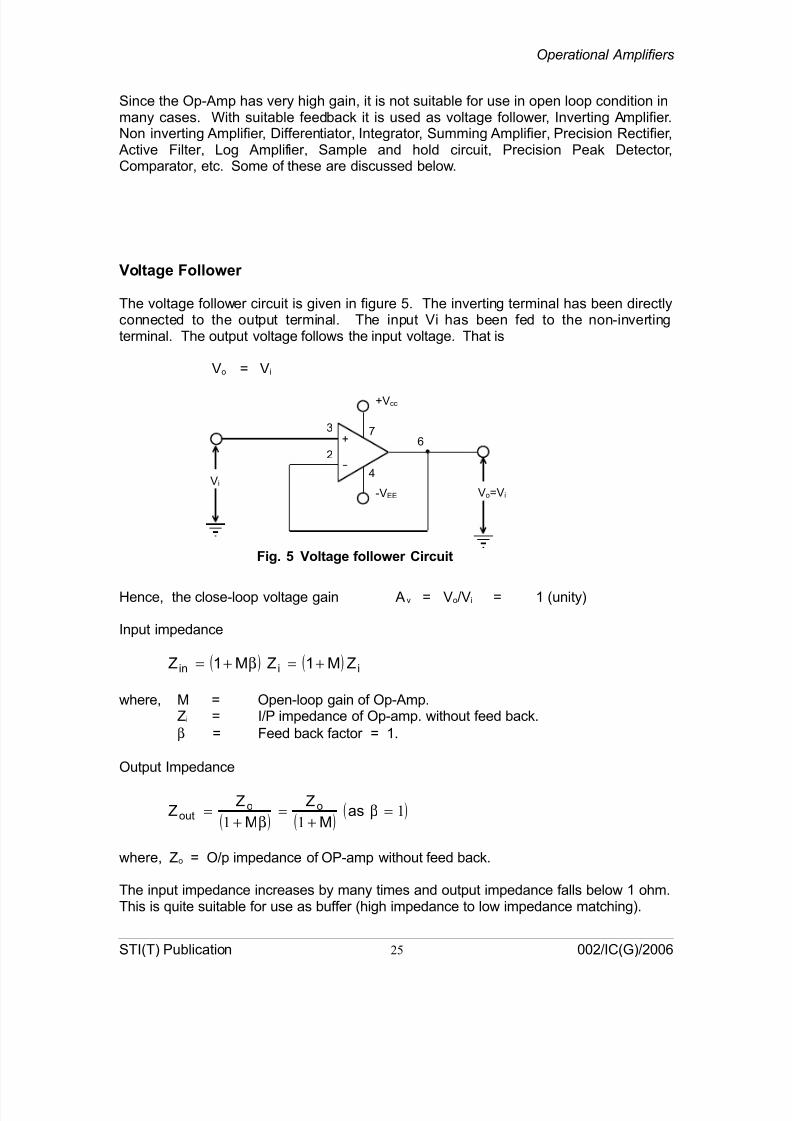
!oltage Follo*er
%he voltage follower circuit is given in figure <. %he inverting terminal has )een directlyconnected to the output terminal. %he input &i has )een fed to the non-invertingterminal. %he output voltage follows the input voltage. %hat is
&o 9 &i
Fig. !oltage follo*er Circuit
&i
&o9&i
+&cc
-&
:
2
=7
;
+
Dence, the close-loop voltage gain Av 9 &o5&i 9 * (unity!
Input impedance
( ) ( ) iiin F>*F>*F +=β+=
where, > 9 Open-loop gain of Op-Amp.Fi 9 I5' impedance of Op-amp. without feed )ack.
β 9 $eed )ack factor 9 *.
Output Impedance
( ) ( ) ( )1
11=β
+=
β+= as
>
F
>
FF oo
out
where, Fo 9 O5p impedance of O'-amp without feed )ack.
%he input impedance increases )y many times and output impedance falls )elow * ohm.%his is "uite suita)le for use as )uffer (high impedance to low impedance matching!.
4%I(%! 'u)lication 25 0025I(6!52007

8/12/2019 02 Operational Amplifier
http://slidepdf.com/reader/full/02-operational-amplifier 6/12
Induction Course (General)
on-in#erting Amplifier
In this configuration, the input is applied to the non-inverting terminal of the Op-Amp andthe feed)ack from output is applied to inverting terminal as shown in figure 7. %his)ehaves in a similar way as the voltage follower circuit of figure <. %he difference is,instead of all the output )eing fed directly )ack to the input, only a portion is fed )ackthrough a potential divider resistors #* and #2.
Fig. / on in#erting Amplifier
&i
+&cc
-&
2
:
= 7
;
-
+
#2
#*
&o 9 &i(* + #25#*! &irtual short
I2
I2
+
-
&#*
+ -
ue to feed )ack from the output terminal 7 the same potential & i is maintained at
terminal 2. In other words, we can say, there is virtual short )etween inverting and non-inverting terminals. %he current I2 flows through #2 and the same current flows through#* (neglecting the very small )ias current into terminal 2!.
Dence,
( )
*
2
*
*2
i
o&
*
i
*2
o
*2
o2*22o
*
i2*2i*#
#
#*
#
##
&
& A,gain&oltage
#
&
##
&
%herefore
##
&I##I&
#
&I#I&&
+=+
==
=+
+=⇒+=
=⇒==
%he input impedance is more than that of open-loop Op-Amp
=β
v A
*
4%I(%! 'u)lication 26 0025I(6!52007
8/12/2019 02 Operational Amplifier
http://slidepdf.com/reader/full/02-operational-amplifier 7/12
Operational Amplifiers
%he output impedance falls )elow that of open loop Op-Amp
=β
v A
*
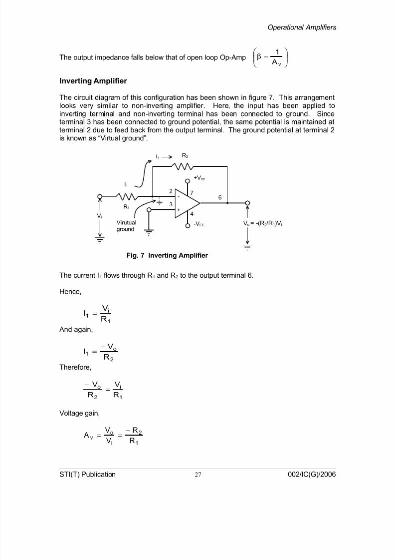
In#erting Amplifier
%he circuit diagram of this configuration has )een shown in figure =. %his arrangementlooks very similar to non-inverting amplifier. Dere, the input has )een applied toinverting terminal and non-inverting terminal has )een connected to ground. 4inceterminal : has )een connected to ground potential, the same potential is maintained atterminal 2 due to feed )ack from the output terminal. %he ground potential at terminal 2is known as “&irtual ground”.
Fig. 0 In#erting Amplifier
&i
+&cc
-&
2
:
= 7
;
-
+
#2
#*
&o 9 -(#25#*!&i
I*
I*
&irutualground
%he current I* flows through #* and #2 to the output terminal 7.
Dence,
*
i*
#
&I =
And again,
2
o*
#
&I
−=
%herefore,
*
i
2
o
#
&
#
&
=
−
&oltage gain,
*
2
i
ov
#
#
&
& A
−==
4%I(%! 'u)lication 27 0025I(6!52007

8/12/2019 02 Operational Amplifier
http://slidepdf.com/reader/full/02-operational-amplifier 8/12
Induction Course (General)
%he negative sign indicates that the output is inverted.
%he input impedance is e"ual to the value of resistance #*.
%he output impedance is similar to that of non-inverting amplifier.
=β
v A
*
Summing Amplifier
%his configuration has )een shown in figure /. %hree inputs have )een connected toinverting terminal. %he output is the sum of all the inputs with gain. %he gain dependson the value of resistors #*, #2, #: and #;. %his circuit functions similar to invertingamplifier.
Fig. Summing Amplifier
+&cc
-&
2
:
=7
;
-
+
#;
#:
&o
#*
#2
&:
&*
&2
!&&&(&then,####if
#
&
#
&
#
&#
#
#&
#
#&
#
#&&
:2*o;:2*
:
:
2
2
*
*;
:
;:
2
;2
*
;*o
++−====
++−=
−
−
−=
Op-Amp as )ifferentiator
%he circuit diagram of differentiator has )een shown in fig. E. %his is similar to invertingamplifier with a capacitor * in the input circuit.
%he current I* flows through #*, * and #2 to the output terminal 7.
4%I(%! 'u)lication 28 0025I(6!52007
8/12/2019 02 Operational Amplifier
http://slidepdf.com/reader/full/02-operational-amplifier 9/12
Operational Amplifiers
Dence,
2
o*
i**
#&I
again And
t
&I
−=
∆∆
=
t
&#&
t
&
#
&
,%herefore
i2*o
i*
2
o
∆∆
−=
∆∆
=−
Fig. 2 Op-Amp as )ifferentiator
&i
+&cc
-&
2
:
= 7
;
-
+
#2
#*
I*
I*
&irtualground
*
#:
-&p
∆&
∆t
+&p
&0 9 -*#2 ∆&
∆t
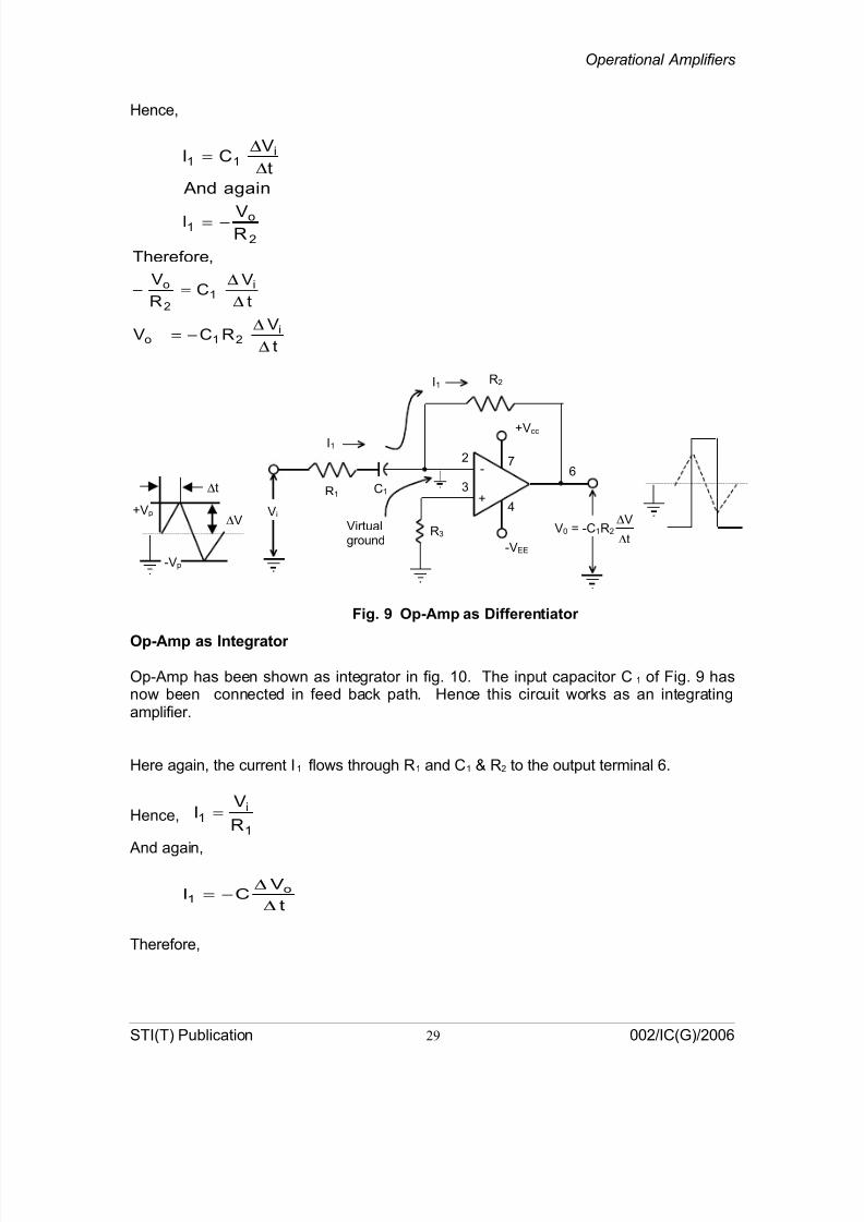
Op-Amp as Integrator
Op-Amp has )een shown as integrator in fig. *0. %he input capacitor * of $ig. E hasnow )een connected in feed )ack path. Dence this circuit works as an integratingamplifier.
Dere again, the current I* flows through #* and * 3 #2 to the output terminal 7.
Dence,*
i*
#
&I =
And again,
t
&I
o
*∆
∆−=
%herefore,
4%I(%! 'u)lication 29 0025I(6!52007

8/12/2019 02 Operational Amplifier
http://slidepdf.com/reader/full/02-operational-amplifier 10/12
Induction Course (General)
*
io
#
&
t
& =
∆∆
−
or
t&#
*&
t&#
*&
i**
o
i**
o
∆∫ −=
∆−=∆
Fig. 13 Op-Amp as Integrator
&i
+&cc
-&
2
:
= 7
;
-
+
#2
#*
t&#
& io ∆∫ −=11
1
I*
&irtualground
*
#:
Application of Operational Amplifier in All India "adio 4 )oordarshan
Operational Amplifier in different configuration has )een e@tensively used in our network.It is difficult to list out all. Dowever, some of these are given )elow 8
S.o. AI"5)) ,6uipment 7sed as
*. AI# $> %ransmitter a! &oltage follower
)! on-inverting Amplifier
c! 4umming Amplifier
d! Integrator
e! 'recision #ectifier
f! omparator
g! Inverting Amplifier
h! Active low pass filter etc.
2. AI# >eltron %# a! Inverting Amplifier
4%I(%! 'u)lication 30 0025I(6!52007

8/12/2019 02 Operational Amplifier
http://slidepdf.com/reader/full/02-operational-amplifier 11/12
Operational Amplifiers
)! on-inverting Amplifier
c! omparator etc.
:. AI# >ultifunction4tereo Audioonsole
a! &oltage follower
)! Inverting Amplifier
c! on-inverting Amplifier
d! 4umming Amplifier
e! ifference Amplifier etc.
;. *0 k D'%&
(>ark II!
a! on-inverting Amplifier
)! Inverting Amplifier
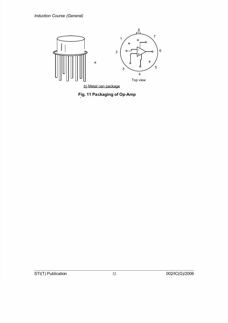
ac8aging of Operational Amplifier
Operational amplifier is generally found in two types of packages. %hey are plastic dual-in-line package (I'! and metal can type package. I' packages are the leaste@pensive and they are more compact than metal can type. 1ut metal can packagedissipates more heat than a plastic type. 1oth type of packages have )een shown)elow in figure **.
-
* 2 : ;
/ = 7 <
+
%op viewa! 'lastic dual-in-line (I'! package
4%I(%! 'u)lication 31 0025I(6!52007
8/12/2019 02 Operational Amplifier
http://slidepdf.com/reader/full/02-operational-amplifier 12/12
Induction Course (General)
-
*
2
:
;
/
=
7
<
+
%op view
)! >etal can package
Fig. 11 ac8aging of Op-Amp
4%I(%! 'u)lication 32 0025I(6!52007