tuprints.ulb.tu-darmstadt.detuprints.ulb.tu-darmstadt.de/7517/1/2018_dissertation_rosenburg.pdf ·...
TRANSCRIPT

The state of carbon and the piezoresistive effect in silicon oxycarbide ceramics
A dissertation approved by the Department of Materials and Earth Sciences in fulfilment
of the requirements for the degree of Doctor−Ingenieur (Dr.-Ing.)
Dipl.-Ing. Felix Rosenburg
Born on 02.07.1984 in Mainz, Germany First assessor: Prof. Dr. Dr. h.c. Ralf Riedel
01.06.2018 – Darmstadt – D-17 Second assessor: Prof. Dr.-Ing Roland Werthschützky

The state of carbon and the piezoresistive effect in silicon oxycarbide ceramics Genehmigte Dissertation von Dipl.-Ing. Felix Rosenburg geb. Roth aus Mainz Fachbereich Material‐ und Geowissenschaften, Technische Universität Darmstadt Jahr der Veröffentlichung der Dissertation auf Tuprints: 2018
1. Gutachter: Prof. Dr. Dr. h. c. Ralf Riedel 2. Gutachter: Prof. Dr.-Ing. Roland Werthschützky Tag der Einreichung: 13.10.2017 Tag der Prüfung: 08.03.2018 Darmstadt D-17
URN: urn:nbn:de:tuda-tuprints-75175
Veröffentlicht unter CC BY-SA 4.0 International https://creativecommons.org/licenses/


Declaration of Authorship
I hereby declare that the thesis submitted is my own unaided work. All direct or indirect sources
used are acknowledged as references.
I am aware that the thesis in digital form can be examined for the use of unauthorized aid and
in order to determine whether the thesis as a whole or parts incorporated in it may be deemed
as plagiarism. For the comparison of my work with existing sources I agree that it shall be
entered in a database where it shall also remain after examination, to enable comparison with
future theses submitted. Further rights of reproduction and usage, however, are not granted
here.
This thesis was not previously presented to another examination board and has not been
published.
Ehrenwörtliche Erklärung
Ich erkläre hiermit ehrenwörtlich, dass ich die vorliegende Arbeit selbständig angefertigt habe.
Die aus fremden Quellen direkt und indirekt übernommenen Gedanken sind als solche
kenntlich gemacht.
Ich weiß, dass die Arbeit in digitalisierter Form daraufhin überprüft werden kann, ob unerlaubte
Hilfsmittel verwendet wurden und ob es sich – insgesamt oder in Teilen – um ein Plagiat
handelt. Zum Vergleich meiner Arbeit mit existierenden Quellen darf sie in eine Datenbank
eingestellt werden und nach der Überprüfung zum Vergleich mit künftig eingehenden Arbeiten
dort verbleiben. Weitere Vervielfältigungs- und Verwertungsrechte werden dadurch nicht
eingeräumt.
Die Arbeit wurde weder einer anderen Prüfungsbehörde vorgelegt noch veröffentlicht.
Darmstadt, den 1. Juni 2018
(Felix Rosenburg)

One of the greatest tragedies in life is the murder of a beautiful theory by a gang of brutal facts.
Benjamin Franklin
Results from the present work were partly disseminated in the following journals:
[1] F. Rosenburg, E. Ionescu, N. Nicoloso, R. Riedel, High-temperature Raman
spectroscopy of nano-crystalline carbon in silicon oxycarbide, Materials, 2018, 11, 93. DOI: 10.3390/ma11010093
[2] L. Tang, F. Rosenburg, N. Nicoloso, R. Werthschützky, Dehnungsmessung an
piezoresistiver polymerabgeleiteter Keramik, tm – Technisches Messen, 2017, 84, 93-97. DOI: 10.1515/teme-2017-0044
[3] F. Roth, P. Waleska, C. Hess, E. Ionescu, N. Nicoloso, UV Raman spectroscopy of
segregated carbon in silicon oxycarbides, J. Ceram. Soc. Japan, 2016, 124, 1042-1045. DOI: 10.2109/jcersj2.16100
[4] F. Roth, C. Schmerbauch, E. Ionescu, N. Nicoloso, O. Guillon, R. Riedel, High-
temperature piezoresistive C/SiOC sensors, J. Sens. Sens. Syst., 2015, 4, 133-136.
DOI: 10.5194/jsss-4-133-2015
[5] F. Roth, C. Schmerbauch, E. Ionescu, N. Nicoloso, O. Guillon, R. Riedel, Piezoresistice
Ceramics for High-Tempature Force and Pressure Sensing, Sensor und Messsystem
2014, Beiträge der 17. ITG/GMA Fachtagung Nürnberg. (ITG-Fachbericht 250), Düsseldorf: VDE-Verl. 2014, ISBN 978-3-8007-3622-5
Other publications:
[6] C. Stabler, F. Roth, M. Narisawa, D. Schliephake, M. Heilmaier, S. Lauterbach,
H.-J. Kleebe, R. Riedel, E. Ionescu, High-temperature creep behaviour of a SIOC glass
ceramic free of segregated carbon, J. Eur. Ceram. Soc., 2016, 36, 3747-3753. DOI: 10.1016/j.jeurceramsoc.2016.04.015
[7] S. Vowinkel, C. G. Schäfer, G. Cherkashinin, C. Fasel, F. Roth, N. Liu, C. Dietz,
E. Ionescu and M. Gallei, 3D-ordered carbon materials by melt-shear organization for
tailor-made hybrid core-shell polymer particle architectures, J. Mater. Chem. C., 2016, 4, 3976-3986. DOI: 10.1039/C5TC03483C
[8] C. Rüttiger, V. Pfeifer, V. Rittscher, D. Stock, D. Scheid, S. Vowinkel, F. Roth,
H. Didzoleit, B. Stühn, J. Elbert, E. Ionescu and M. Gallei, One for all: Cobalt-
Containing Polymethacrylates for Magnetic Ceramics, Block Copolymerization,
Unexpected Electrochemistry, and Stimuli-Responsivness, Polym. Chem., 2016, 7, 1129-1137. DOI: 10.1039/C5PY01845E

i
Table of Content
TABLE OF CONTENT ........................................................................................................ I
ABSTRACT...................................................................................................................... III
ZUSAMMENFASSUNG ................................................................................................... V
1 MOTIVATION AND AIM OF THE STUDY ................................................................. 1
2 STATE OF THE ART AND BASICS OF PIEZORESISTIVE CERAMICS .......................... 3
2.1 POLYMER DERIVED CERAMICS ............................................................................................. 3
2.1.1 The SiOC/C system ................................................................................................ 4
2.1.2 The microstructure of SiOC/C ................................................................................ 6
2.1.3 Percolation within SiOC/C. .................................................................................... 7
2.2 ELECTRICAL CONDUCTIVITY IN SIOC/C .............................................................................. 10
2.2.1 The allotropes of carbon and their unique electrical properties ......................... 10
2.2.2 Electrical conductivity in semiconductive carbon structures ................................ 14
2.2.3 Graphitization of carbon ..................................................................................... 18
2.3 THE PIEZORESISTIVE EFFECT .............................................................................................. 19
2.3.1 Piezoresistivity in crystalline semiconductors ...................................................... 20
2.3.2 Piezoresistvity in carbon ...................................................................................... 22
2.3.3 Piezoresistive carbon-containing inorganic nanocomposites .............................. 23
3 EXPERIMENTAL PROCEDURE ................................................................................. 29
3.1 SAMPLE PREPARATION .................................................................................................... 29
3.2 MATERIALS CHARACTERIZATION ....................................................................................... 31
3.2.1 Elemental analysis ............................................................................................... 31
3.2.2 Density and porosity measurements ................................................................... 32
3.2.3 Raman spectroscopy ........................................................................................... 32
3.2.4 Thermogravimetric analysis ................................................................................. 33
3.2.5 X-ray diffraction .................................................................................................. 33
3.2.6 X-ray photoelectron spectroscopy ...................................................................... 34
3.2.7 Scanning Electron Microscope ............................................................................ 34
3.3 ELECTRICAL INVESTIGATIONS ............................................................................................ 34
3.3.1 Electrical contacting of the samples .................................................................... 34
3.3.2 Temperature dependent impedance spectroscopy............................................. 35
3.3.3 Piezoresistive measuring chamber ...................................................................... 35
3.3.4 High-temperature piezoresistive setup ............................................................... 36
3.3.5 Hall measurements .............................................................................................. 37
4 RESULTS AND DISCUSSION ................................................................................... 38
ii
4.1 STRUCTURAL CHARACTERIZATION AND THERMAL STABILITY OF SIOC/C ................................. 38
4.1.1 Phase composition .............................................................................................. 38
4.1.2 Densification process .......................................................................................... 42
4.1.3 Crystallization and bonding situation ................................................................. 44
4.1.4 Impact of oxidation on the electrical conductivity ............................................. 49
4.1.5 Summary ............................................................................................................. 50
4.2 RAMAN SCATTERING IN CARBON MATERIALS ...................................................................... 51
4.2.1 Monitoring the graphitization process in SiOC/C ............................................... 53
4.2.2 Characterization of the segregated carbon phase by Vis Raman ....................... 57
4.2.3 Summary ............................................................................................................. 63
4.3 ELECTRICAL PROPERTIES OF SIOC/C .................................................................................. 64
4.3.1 Resistance change with graphitization ............................................................... 65
4.3.2 Percolation in SiOC/C .......................................................................................... 65
4.3.3 Conduction mechanism in SiOC/C ...................................................................... 68
4.3.4 Hall measurements of SiOC/C ............................................................................. 72
4.3.5 Summary ............................................................................................................. 74
4.4 THE PIEZORESISTIVE EFFECT IN SIOC/C .............................................................................. 75
4.4.1 Effect of carbon concentration on the piezoresistive behavior .......................... 77
4.4.2 Effect of temperature on the piezoresistive behavior ........................................ 82
4.4.3 Origin of the piezoresistve effect in SiOC/C ....................................................... 85
4.4.4 Comment on giant gauge factors in PDCs reported in literature ....................... 85
4.4.5 Development and application of a SiOC/C based prototype ............................. 87
4.4.6 Summary ............................................................................................................. 90
5 CONCLUSION & OUTLOOK .................................................................................... 91
6 REFERENCES ........................................................................................................... 93
ACKNOWLEDGMENT .................................................................................................. 101
LIST OF ABBREVIATIONS ............................................................................................ 102
LIST OF SYMBOLS ....................................................................................................... 104
LIST OF FIGURES ......................................................................................................... 106
LIST OF TABLES ........................................................................................................... 108
CURRICULUM VITAE ................................................................................................... 109

iii
Abstract
The present work reports on the morphology of carbon, the electrical properties and the
piezoresistve effect in polymer-derived silicon oxycarbides (SiOC/C nanocomposites) within
carbon concentrations of 1 < C < 45 vol.%. The nanocomposites have been prepared by
pyrolysis of poly-organosilicon precursors or preceramic polymers and a subsequent
densification step using spark plasma sintering (1000 < T < 1800 °C; P = 50 MPa, Argon). The
obtained samples are characterized by the means of spectroscopic (Raman, TGA-FTIR, XRD,
XPS) and electrical (dc conductivity, impedance, Hall effect) investigations. The SiOC/C
composites consist of a glassy matrix (silica, SiOxC4-x), silicon carbide and segregated carbon
and is simplified as a two phase system (glass/carbon) for the description of the electrical and
piezoresistive properties. The state of carbon within SiOC/C depends on the carbon content of
the precursor and the thermal treatment. According to UV Raman the microstructure of carbon
changes from a disordered (amorphous) to nano-crystalline state within 1000 < T < 1800 °C.
The progressive ordering or graphitization, respectively, is illustrated by the increasing lateral
crystal size (7.5 < La < 20 nm) and the corresponding decrease of the density of defects as
derived from the intensity ratio AD/AG of the Raman D- and G-band. Vacancies have been
identified as main type of defects.
The electrical and piezoresitive properties of SiOC/C mainly depend on the state of carbon with
the exception of samples with very low carbon content (C < 1 vol.%). For samples treated at
T = 1600 °C the resistivity decreases by several orders of magnitude at a critical carbon
concentration of about 6 vol.%. For samples treated at 1400 and 1100 °C the percolation
threshold shifts from 8 to 20 vol.% of carbon because of the lower degree of graphitization.
Beyond the percolation threshold weakly activated transport (Ea < 0.1 eV) occurs in conjugated
sp² bonds within a continuous 3D network. The charge carrier mobility (µ ≈ 3 cm²/Vs) and
density (N = 1018 – 1020 cm-³) of carriers are comparable to those of glassy carbon. A change
from band-like transport to conduction in localized states at the percolation threshold is
indicated by an increase in Ea ≈ 0.3 eV and presumably arises from electron/hole confinement
when the localization length approaches a lateral crystal size of La ≲ 10 nm (La decreases from
about 8 to 4 nm within 1 < C < 10 vol.% carbon).
SiOC/C changes its resistivity with strain and, accordingly, the piezoresistive effect also relies
on the carbon content and its degree of graphitization. Within 1 < C < 6 vol.% the gauge factor
(GF) increases up to the percolation threshold (GF ≈ 45) and appears to arise from charge
carrier tunneling. The extremely high GF values (> 1000) at the percolation threshold suggest
either divergence of the GF vs. carbon concentration function or local strain concentration with

iv
local deviating from bulk by an enhancement factor. Above the percolation threshold GF is
related to the density of defects within the continuous carbon network. A strain-induced
increase of the density of states near EF is identified as origin of the piezoresistive effect, a
change in mobility is unable to explain the experimental decrease of the resistance with applied
strain.
The obtain results on the piezoresistivity favor the development of high-temperature strain
sensors able to detect static and dynamic excitation. As a proof of concept a demonstrator to
sense the natural frequency of a planetary gear has been developed.

v
Zusammenfassung
Die vorliegende Arbeit widmet sich der Beschreibung der Mikrostruktur des Kohlenstoffs, den
elektrischen Eigenschaften und dem piezoresistivem Verhalten von Polymer-abgeleiteten
Siliciumoxycarbid (SiOC/C) Nanokompositen mit einer Kohlenstoffkonzentration im Bereich
von 1 < C < 45 vol.%. Die Nanokomposite werden mittels direkter Polymer-zu-Keramik
Umwandlung synthetisiert wobei poly-organosilikone und präkeramische Polymere zunächst
pyrolysiert und anschließend verdichtet werden (Spark Plasma Sintering,
1000 < T < 1800 °C; P = 50 MPa, Argon). Mit Hilfe spektroskopischer (Raman, TGA-FTIR,
XRD, XPS) und elektrischer (Gleichstromwiderstand, Impedanz, Hall Effekt) Untersuchungen
werden die jeweiligen Proben charakterisiert. Die Proben setzen sich aus einer glasartigen
Matrix (Silica, SiOxC4-x), Siliciumcarbid und einer segregierten Kohlenstoffphase zusammen
und werden, um die elektrischen und piezoresistiven Eigenschaften zu beschreiben,
nährungsweise als ein Zweikomponentensystem (Glass/Kohlenstoff) betrachtet. Der Zustand
des Kohlenstoffs in SiOC/C hängt von dem Kohlenstoffanteil des verwendeten Präkursors und
der thermischen Behandlung ab. Wie die UV Raman-Untersuchungen belegen, wandelt sich die
Kohlenstoffphase von einem ungeordneten (amorphen) in einen nanokristallinen Zustand
innerhalb des Temperaturbereichs 1000 < T < 1800 °C um. Die fortschreitende Ordnung oder
Graphitisierung wird durch die zunehmende laterale Kristallitgröße (7.5 < La < 20 nm) und
der damit zusammenhängenden Abnahme der Defektdichte, welche aus dem AD/AG Verhältnis
der Raman D- und G-Banden abgeleitet werden kann, verdeutlicht. Leerstellen innerhalb der
Kohlenstoffphase werden als wesentliche Art der Defekte identifiziert.
Im Gegensatz zu Proben mit sehr geringem Kohlenstoffanteil (C < 1 vol.%) werden die
elektrischen und piezoresistiven Eigenschaften von SiOC/C hauptsächlich von dem Zustand des
Kohlenstoffs bestimmt. Für Proben hergestellt bei T = 1600 °C nimmt der elektrische
Widerstand um mehrere Größenordnungen ab, wenn der Kohlenstoffanteil die kritische
Konzentration von 6 vol.% überschreitet. Proben, die hingegen bei 1000 oder 1400 °C
synthetisiert wurden, besitzen eine deutlich höhere Perkolationsgrenze von 20 und 8 vol.%, da
die Kohlenstoffphase schwächer graphitisiert vorliegt. Oberhalb der Perkolationsgrenze wird
der schwach aktivierte (Ea < 0.1 eV) elektrische Transport durch konjugierter sp²-Bindungen
innerhalb des durchgängigen dreidimensionalen Kohlenstoffsnetzwerk realisiert. Die
Ladungsträgermobilität (µ ≈ 3 cm²/Vs) und Dichte der Ladungsträger (N = 1018 – 1020 cm-³)
entspricht der von glasartigen Kohlenstoff. An der Perkolationsgrenze wechselt der elektrische
Leitungsmechanismus von einem bandähnlichem Transport zu einem Transport innerhalb
lokalisierter Zuständen, was durch ein Anstieg in der Aktivierungsenergie (Ea ≈ 0.3 eV)

vi
verdeutlicht wird. Dies resultiert wahrscheinlich aus einer Elektronen/Locheinschränkung
sobald sich die Lokalisierungslänge, der Kristallitgröße von La ≲ 10 nm nähert (La sinkt im
Bereich von 1 < C < 10 vol.% Kohlenstoff von 8 auf 4 nm).
SiOC/C verändert unter Druck seinen elektrischen Widerstand, weshalb der piezoresistive
Effekt folglich mit dem Anteil an Kohlenstoff und dessen Graphitisierungszustand
zusammenhängt. Innerhalb 1 < C < 10 vol.% Kohlenstoff steigt der gauge Faktor (GF) bis zur
Perkolationsgrenze (GF ≈ 45) und scheint mit Tunnelprozessen der Ladungsträger verbunden
zu sein. Extrem hohe GF Werte (> 1000) an der Perkolationsgrenze suggerieren entweder eine
Divergenz der GF-Funktion, oder erhöhte lokale Belastung local, welche um einen
Verstärkungsfaktor von der Belastung innerhalb des Probe bulk abweichen. Oberhalb der
Perkolationsgrenze hängt GF von der Defektdichte innerhalb des durchgehenden
Kohlenstoffnetzwerkes ab. Eine durch Belastung induzierte erhöhte Zustandsdichte nahe EF
wurde als Ursache für das piezoresistive Verhalten ermittelt, welches durch eine Änderung der
Ladungsträgermobilität nicht erklärt werden kann.
Ausgehend von den piezoresistiven Ergebnissen lässt sich ein hochtemperaturstabiler
Drucksensor entwickeln, welcher sowohl statisch als auch dynamisch Anregungen detektieren
kann. Auf Basis der ermittelten Ergebnisse wurde ein Prototyp entwickelt, welcher die
Eigenfrequenz eines Planetengetriebes detektiert.

1 Motivation 1
1 Motivation and aim of the study
A clean and efficient combustion process is especially nowadays, in view of the climate change,
the key to reduce fossil fuel consumption and CO2 emission. While low-carbon fuels or the
deployment of hybrid and electric vehicles present viable alternatives, the majority of
propulsion systems operating today still use conventional fuels associated with the internal
combustion engine. Hence, the understanding of the physical and chemical basics of the
combustion process is fundamental to achieving improvements in fuel efficiency, reducing
greenhouse gas emissions and moreover allows for intelligent propulsion system design and
enhancement of system maintenance and safety. In order to achieve insights into the
combustion process innovative high-temperature stable sensor materials are required as the
sensor needs to be located as close as possible to the desired measurand for accurate
monitoring. However, conventional microelectromechanical systems (MEMS) are not capable
of operating under these harsh conditions and thus need to be located outside the combustion
chamber. The limitation of non-direct sensing induces inaccuracy and underlines the critical
need of high-temperature sensing technology in nearly all industrial sectors such as automotive,
aerospace and energy industry.
The most common sensing techniques considered in high-temperature applications are:
capacitive, piezoelectric and piezoresistve. Capacitive sensors usually consist of two separated
plates whose distance changes upon the applied stress leading to a change in capacitance. This
kind of sensor is known to exhibit a low thermal shift, a high resolution and a low background
noise. Yet they suffer from limited robustness and are easily disturbed by parasitic capacitance
with magnitudes similar to that of the sensor signal. Piezoelectric sensors have been intensively
studied in the recent years. Due to their crystalline structure most of the materials only possess
piezoelectric behavior along one certain crystal plane. In case of polycrystalline material they
need to be post treated in an electric field to induce polarisation. Furthermore, phase transition
and oxygen diffusion often lead to a low quality signal limiting the sensing performance to
temperatures below T < 400 °C.
Piezoresistive sensors utilize the change in electrical resistivity upon mechanical strain and have
the advantage to provide accurate dynamic and static measurements. Metallic strain gauges
and semiconductive materials (Si, Ge) are generally used in commercially available
piezoresistive sensors but often suffer from a high fragility and rigidity. Therefore, polymer-
based composites filled with conductive particles appear preferable for a broader range of
applications. In particular carbon nanotubes (CNTs) polymer composites are already broadly

2 1 Motivation
used as mechanical strain sensors. However, due to their polymeric nature, the application
temperature is limited and the composites often suffer from agglomeration.
Within this work, polymer-derived ceramics (PDCs) are introduced to eliminate the problems
of agglomeration and temperature limitation as they are known to withstand harsh
environments. Previous work revealed that PDCs exhibit promising piezoresistive behavior
which makes them an auspicious future candidate material in sensor technology under harsh
conditions. No-post treatment is necessary for the piezoresistve behavior to occur, as it solely
relies on the homogeneous in-situ segregation of carbon during the polymer-to-ceramic
transformation. To date, only a few scientific publications deal with the piezoresistive effect
and the electrical properties of PDCs.
The present thesis provides a comprehensive study of the microstructural and electrical
properties of polyorganosiloxane derived silicon oxycarbide ceramics (SiOC/C) to prove their
deployment as prospective piezoresistive sensor materials. The changes of the electrical
properties are investigated as a function of synthesis temperature and varying carbon
concentrations. Aim of the study is to present a comprehensive description of the piezoresistive
effect in SiOC/C nanocomposites and to demonstrate their application as strain sensors under
static and dynamic conditions at room and elevated temperatures.

2 State of the art and basics of piezoresistive ceramics 3
2 State of the art and basics of piezoresistive ceramics
The first section of this chapter delivers a brief introduction into the SiOC/C system and its
microstructure. In the following, their electrical properties and the different conduction
mechanisms of various carbon allotropes will be discussed in detail. Finally, an insight into the
basic principles of the piezoresistive effect and the current research on piezoresistive, inorganic
carbon-composites will be provided.
2.1 Polymer derived ceramics
In 1956, Fritz and Raabe discovered that monomeric organosilicon compounds (Si(CH3)4 and
Si(C2H5)4) can be thermally transformed into a SiC ceramic at much lower temperatures as
compared to the traditional synthesis methods [1]. A few years later, in the early 1960 Ainger
and Herbert [2] as well as Chantrell and Popper [3] reported on the thermal conversion of
polyphosphazene ((NPCl2)n) into a P3N5 ceramic. The first technical approach was defined by
Verbeek, Winter and Mansmann [4-6] almost ten years later, as they described the production
of small-diameter Si3N4/SiC fibers upon thermolysis of organosilicon polymers. A significant
breakthrough was achieved at the end of the 1970s, when Yajiima et al. developed a method to
fabricate SiC based fibers [7-9]. These initial discoveries and the first successful technical
approach promoted the growing interest for this novel synthesis route and led to further
developments of new precursors and improved processing techniques. The era between 1950
and 1980 can be marked as the origin of a novel class of ceramic materials, the so-called
polymer-derived ceramics (PDCs).
Especially, polysiloxane, polysilazan and polycarbosilane have proven to be the most important
preceramic polymers. Figure 2.1 displays the Si-based preceramic polymers and their thermal
conversion to their correlating ceramic microstructure.
The final ceramic composition is mainly determined by the chemistry and structure of the
preceramic polymer. Accordingly, different ceramic systems such as binary SiC and Si3N4 or
ternary SiOC and SiCN systems can be achieved depending on the chemical element (X = Si,
C, N, O) are bonded to the backbone of the starting polymer. It is important to note that the
latter systems cannot be synthesised by traditional processing methods, due to the low solubility
of carbon in SiO2 and Si3N4. In addition, the family of ternary systems can easily be extended
to a broad variety of quaterny and even multi-nary ceramics by a simple chemical modification
of the preceramic polymer with elements such as: Al, B, Hf, Zr or Ti [10-18].

4 2 State of the arte and basics of piezoresistive ceramics
Figure 2.1: Simplified structure of silicon based polymer. By substituting the polymeric backbone atom X
with C, O or N different types of ceramics structures can be achieved upon pyrolysis [19].
Not only does the chemistry of preceramic polymer correlate with the resulting ceramic
microstructure, it also allows to tailor the properties of the starting polymer like rheology,
solubility and decomposition. A broad variety of designed ceramics can be processed or shaped
using established forming techniques in plastic industry such as polymer infiltration, injection
molding, coating from solvent, extrusion or resin transfer molding [19]. In addition, no
sintering additives or agents have to be used during the polymer-to-ceramic process which
further facilitates their application.
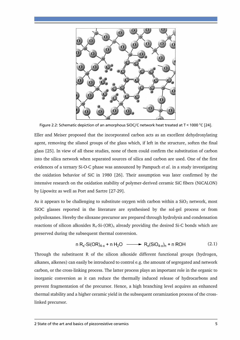
2.1.1 The SiOC/C system
A silicon oxycarbide compound (SiOC) prepared at T < 1000 °C is a covalent network of silicon
tetrahedra bonded to carbon and oxygen atoms. Their chemical structure can be derived from
silica glass in which part of the oxygen atoms are replaced by carbon atoms solely bonded to
silicon. Besides the amorphous network, generally described by SiO4-xCx (x = 1 - 4), a fine
dispersed carbon phase (“segregated carbon”) might be present, depending on the carbon
content of the initial precursor. The so-called “carbon rich” silicon oxycarbides (SiOC/C)
therefore inhibit two types of carbon atoms: sp3hybridized carbon within the amorphous matrix
and sp2-type segregated carbon. A schematic depiction of the silicon oxycarbide structure is
given in Figure 2.2. As a result of the incorporation of carbon, C(Si)4 units are locally formed,
which strengthens the network and thus enhance several material properties like viscosity,
glass-transition temperature and Young’s modulus [20, 21].
One of the first attempts to incorporate carbon into glass was investigated by Ellis in 1951 in
order to lower the electrical resistance of silica [22]. In 1968 Smith and Crandall reported on
the increasing resistance of devitrification and higher viscosity when a mixture of carbonwax
and colloidal silica was hot-pressed at T = 1000 - 1150 °C under P = 138 bar [23].
2 State of the art and basics of piezoresistive ceramics 5
Figure 2.2: Schematic depiction of an amorphous SiOC/C network heat treated at T < 1000 °C [24].
Eller and Meiser proposed that the incorporated carbon acts as an excellent dehydroxylating
agent, removing the silanol groups of the glass which, if left in the structure, soften the final
glass [25]. In view of all these studies, none of them could confirm the substitution of carbon
into the silica network when separated sources of silica and carbon are used. One of the first
evidences of a ternary Si-O-C phase was announced by Pampuch et al. in a study investigating
the oxidation behavior of SiC in 1980 [26]. Their assumption was later confirmed by the
intensive research on the oxidation stability of polymer-derived ceramic SiC fibers (NiCALON)
by Lipowitz as well as Port and Sartre [27-29].
As it appears to be challenging to substitute oxygen with carbon within a SiO2 network, most
SiOC glasses reported in the literature are synthesised by the sol-gel process or from
polysiloxanes. Hereby the siloxane precursor are prepared through hydrolysis and condensation
reactions of silicon alkoxides Rx-Si-(OR)x already providing the desired Si-C bonds which are
preserved during the subsequent thermal conversion.
(2.1)
Through the substituent R of the silicon alkoxide different functional groups (hydrogen,
alkanes, alkenes) can easily be introduced to control e.g. the amount of segregated and network
carbon, or the cross-linking process. The latter process plays an important role in the organic to
inorganic conversion as it can reduce the thermally induced release of hydrocarbons and
prevent fragmentation of the precursor. Hence, a high branching level acquires an enhanced
thermal stability and a higher ceramic yield in the subsequent ceramization process of the cross-
linked precursor.

6 2 State of the arte and basics of piezoresistive ceramics
2.1.2 The microstructure of SiOC/C
Upon thermal treatment at temperatures below T < 1000 °C, an amorphous structure of two
interwoven networks emerge: the amorphous SiOC phase which consists of mixed silicon
tetrahedral units and the in-situ generated “segregated” carbon phase. Saha. et al. proposed a
microstructural model where silica-rich nanodomains in the size of 1 – 3 nm are embedded into
a percolative network of graphene-like sheets [30]. The interdomain boundaries between both
phases are connected through mixed SiOxC4-x tetrahedral units like SiC3O, SiC2O2 and SiCO3. A
more recent topological model proposes a spatial segregation of the structural SiOxC4-x-units
into oxygen-rich and the carbon-rich SiCxO4-x units [31]. This assumption relies on the
observation that the concentrations of SiO4 and SiC4 units are significantly higher than those
expected from a statistical distribution of Si-O and Si-C bonds in SiOC. The oxygen-rich
structural units are supposed to constitute the interior backbone of the amorphous ceramic
while the carbon-rich units occupy the interface between the ceramic backbone and the
segregated carbon phase. Both structural models are depicted in Figure 2.3.
Figure 2.3: Two proposed models of the nanostructure in polymer-derived SiOC. a) Silica nanodomains
are warped by layers of graphene [32]. b) O2-rich SiOC domains form a continuous network and
encapsulate the precipitated carbon [33].
Upon further annealing T > 1300 °C, the SiOC network demixes forming nanodomains of
amorphous silica and silicon carbide. Due to the fact that the silica domains are amorphous and
do not tend to crystallize into cristoballite, even at high temperatures (T > 1800 °C), the
crystallization process of silica in SiOC/C is most probably supressed. A low interfacial energy
between SiC and SiO2 and the presence of a finely dispersed carbon phase obstructing long-
range diffusion in silica were proposed as cause for the enhanced crystallization resistance [32].
However, the crystallization of SiOC into β-SiC seems not to be hindered and can occur by the
following two reactions: (i) in the first process at temperatures above T > 1300 °C the
amorphous SiOC separates into amorphous silica an silicon carbide which is then followed by
crystallization of the latter. (ii) The second pathway appears only after the phase separation at
temperatures above T > 1500 °C and includes the reduction of silica using carbon as reduction
2 State of the art and basics of piezoresistive ceramics 7
agent. The nanometer sized β-SiC crystals were found to appear near carbon structures with an
average crystal size less than 5 nm [34, 35]. Both reactions may appear in combination at
sufficiently high temperatures.
(2.2)
(2.3)
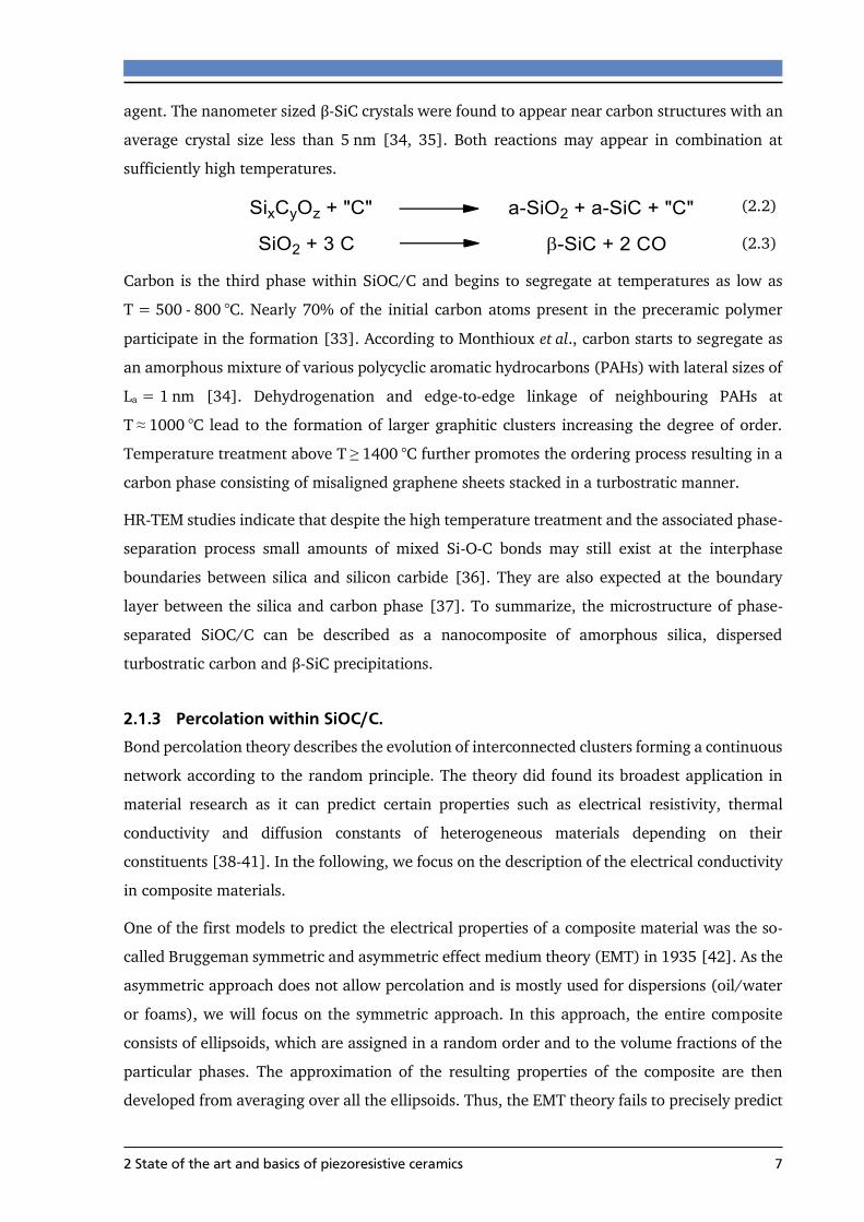
Carbon is the third phase within SiOC/C and begins to segregate at temperatures as low as
T = 500 - 800 °C. Nearly 70% of the initial carbon atoms present in the preceramic polymer
participate in the formation [33]. According to Monthioux et al., carbon starts to segregate as
an amorphous mixture of various polycyclic aromatic hydrocarbons (PAHs) with lateral sizes of
La = 1 nm [34]. Dehydrogenation and edge-to-edge linkage of neighbouring PAHs at
T ≈ 1000 °C lead to the formation of larger graphitic clusters increasing the degree of order.
Temperature treatment above T ≥ 1400 °C further promotes the ordering process resulting in a
carbon phase consisting of misaligned graphene sheets stacked in a turbostratic manner.
HR-TEM studies indicate that despite the high temperature treatment and the associated phase-
separation process small amounts of mixed Si-O-C bonds may still exist at the interphase
boundaries between silica and silicon carbide [36]. They are also expected at the boundary
layer between the silica and carbon phase [37]. To summarize, the microstructure of phase-
separated SiOC/C can be described as a nanocomposite of amorphous silica, dispersed
turbostratic carbon and β-SiC precipitations.
2.1.3 Percolation within SiOC/C.
Bond percolation theory describes the evolution of interconnected clusters forming a continuous
network according to the random principle. The theory did found its broadest application in
material research as it can predict certain properties such as electrical resistivity, thermal
conductivity and diffusion constants of heterogeneous materials depending on their
constituents [38-41]. In the following, we focus on the description of the electrical conductivity
in composite materials.
One of the first models to predict the electrical properties of a composite material was the so-
called Bruggeman symmetric and asymmetric effect medium theory (EMT) in 1935 [42]. As the
asymmetric approach does not allow percolation and is mostly used for dispersions (oil/water
or foams), we will focus on the symmetric approach. In this approach, the entire composite
consists of ellipsoids, which are assigned in a random order and to the volume fractions of the
particular phases. The approximation of the resulting properties of the composite are then
developed from averaging over all the ellipsoids. Thus, the EMT theory fails to precisely predict

8 2 State of the arte and basics of piezoresistive ceramics
the filler concentration at which the composite acquires electrical conductivity due to the fact
that it is a volume-weighted model averaging the properties of the constitutes and ignoring any
fractal or long-range correlations. Therefore, the theory has only proven to fairly model
electrical percolation in two dimensions [43].
As the insulator-conductor transition does not behave linearly near the percolation threshold, a
more precise phenomenological description of the change in electrical conductivity has to be
formulated, namely the percolation theory (PT) [39]. Consider fillers with high electrical
conductivity added continuously to an insulating matrix. The insulator-conductor transition is
then described by the evolution of a continuous pathway throughout the matrix as the filler
concentration C approaches a critical volume cri. also called percolation threshold. At the
threshold, the first percolating path is formed throughout the insulating matrix resulting in an
abrupt increase in the electrical conductivity. The overall conductivity of the composite near
the percolation threshold can be expressed according to
𝜎𝐶 = 𝜎0 ∙ ( − 𝑐𝑟𝑖.
)𝑡 (2.4)
where σ0 is a proportionality constant, σC the conductivity of the composite, cri. the critical
concentration below the composite is insulating (percolation threshold) and t the critical
exponent. The value of the critical exponent t is known to depend on the lattice dimensionality
and was calculated to be t ≈ 2.0 in a three-dimensional lattice [44, 45]. Derivation from this
behavior have been reported for many different composites [46]. According to Balberg this
derivation can be assigned to a tunnelling-percolation processes with strong fluctuations in
tunnelling distances causing high values even up to t = 6.0 [47, 48].
The electrical conductivity of a SiOC/C nanocomposite is determined by the volume fraction
and morphology of its carbon segregations. In order to consider the influence of these two
factors, Cordelair et al. simulated the insulator-conductor transition of SiOC/C by using the
general effective media theory (GEM). The GEM combines most aspects of the EMT and PT
theory and thus allows to assess the influence of the amount and the different graphitization
states of the carbon phase as depicted in Figure 2.4. Following the proposed model by Cordelair
et al., the conductivity in SiOC/C can be divided into two regions: the tunnelling regime at low
carbon concentrations and the percolation regime [49]. Below the percolation threshold the
conductivity is driven by hopping and tunnelling processes between randomly distributed
carbon segregations whereas above the percolation threshold a conductive pathway throughout
the insulating matrix is present, entering the percolation regime. To account for the distinct
carbon morphologies which depend on the applied pyrolysis temperatures, t was varied

2 State of the art and basics of piezoresistive ceramics 9
between 2 – 4 and the percolation threshold was set from cri. = 20 – 5 vol.% carbon.
Accordingly, at low pyrolysis temperatures (T < 800 °C) a high amount of segregated carbon is
necessary to build a conductive pathway due to the low aspect ratio of the presumably spherical-
like carbon segregation. This was simulated by a high percolation threshold of cri. = 20 vol.%
and a low critical exponent of t = 2. Increasing the pyrolysis temperature results in a growing
aspect ratio of the carbon precipitations which is expressed by a decreasing percolation
threshold cri. = 5 vol.% and an increasing critical exponent of t = 4.0. Therefore, the insulator-
conductor transition is realized at much lower carbon concentrations for samples pyrolyzed at
higher temperatures. Additionally, the authors observed that with increasing aspect ratio the
abrupt rise in conductivity at the percolation threshold appeared to be less intense and that the
overall conductivity of the SiOC/C material below the percolation threshold was enhanced.
Thus, the resulting conductivity and the percolation threshold respectively, can be adjusted by
choosing different pyrolysis temperatures as the aspect ratio of the carbon segregations is
enhanced.
Figure 2.4: Calculated insulator-conductor transition for different values of t and cri. [49].
A precise prediction of the electrical conductivity of a SiOC/C system is rather challenging as
reliable information about its carbon morphology and aspect ratio are difficult to acquire.
Besides, the closer the SiOC/C system is to the percolation threshold the stronger the
conductivity is influenced by small concentration variations. Therefore, we concentrated on
carbon-rich SiOC/C systems (C > 10 vol.%) just above the percolation threshold to minimize
the influence of the process parameter and to increase their reproducibility.

10 2 State of the arte and basics of piezoresistive ceramics
2.2 Electrical conductivity in SiOC/C
The overall conductivity of PDCs is mainly determined by the concentration and graphitization
state of the segregated carbon phase which enables to specifically tailor their electrical behavior.
A recently reported SiOC/C ceramic [50] with a high carbon content (C ≈ 30 vol.%) showed a
resistivity value of ρ = 0.35 Ω/m at RT which further decreased to ρ = 0.14 Ω/m upon
annealing (note that graphite has a resistivity of ρ ≤ 10-3 Ω/m). These values are significantly
lower than those usually reported for SiOC with a carbon content C < 7.5 vol.%
(ρ = 107 - 1010 Ω/m) [49]. The change in resistivity is attributed to the higher amount of
segregated carbon. Besides the amount of segregated carbon, its degree of order is considered
to significantly affect the electrical conductivity as all experimental studies show an increase of
conductivity with increasing pyrolysis temperature [51-53] or increasing graphitization,
respectively. In the following we will consider the different allotropes of carbon and their
change in microstructure and conductivity respectively upon graphitization, as the carbon phase
possess the most prominent influence on the electrical conductivity in SiOC/C.
2.2.1 The allotropes of carbon and their unique electrical properties
Elemental carbon is well known to possess a broad variety of allotropes with different electrical,
thermal and mechanical properties. Depending on the structure and its hybridization state, the
electrical conductivity can vary between a strong insulator (diamond) and a highly conductive
material (graphite). This emphasizes the strong correlation between the microstructure and
electrical conductivity in carbon materials.
Besides the crystalline structures, various types of disordered carbons such as turbostratic
carbon, glassy carbon or diamond-like-carbon (DLC) and their hydrogenated analogous exist.
Their properties can be assigned according to the following principles: (i) the ratio of sp² and
sp³ sites, (ii) the local arrangement and (iii) the concentration of the hydrogen atoms. A
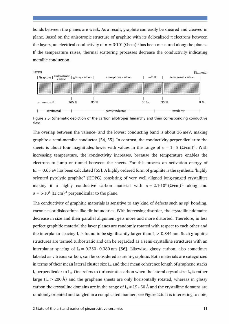
schematic representation of selected carbonaceous allotropes is given in Figure 2.5. Note that
the amount of sp² carbon and the electrical behavior are broad estimations, as they strongly
depend on the synthesis method and the applied heat-treatment.
Graphite consists of solely sp² hybridized carbon layers stacked in a hexagonal ABA order. The
carbon layers (graphene) are weakly bounded together by Van-der Waals forces produced by
the delocalized π-orbitals of each sheet. The reason why elemental carbon favors the graphitic
structure in contrast to other group IV elements, which prefer to coordinate along the diamond
lattice, is its electronic state and the fact that all first row elements lack of p-like core electrons.
This results in tightly contracted p-orbitals, enhancing the covalent sigma bonds of the sp²
carbon. Therefore, the bonds along the basal plane are extremely stiff and strong, whereas the
2 State of the art and basics of piezoresistive ceramics 11
bonds between the planes are weak. As a result, graphite can easily be sheared and cleaved in
plane. Based on the anisotropic structure of graphite with its delocalized π electrons between
the layers, an electrical conductivity of σ = 3∙104 (Ω∙cm)-1 has been measured along the planes.
If the temperature raises, thermal scattering processes decrease the conductivity indicating
metallic conduction.
Figure 2.5: Schematic depiction of the carbon allotropes hierarchy and their corresponding conductive
class.
The overlap between the valence- and the lowest conducting band is about 36 meV, making
graphite a semi-metallic conductor [54, 55]. In contrast, the conductivity perpendicular to the
sheets is about four magnitudes lower with values in the range of σ = 1 - 5 (Ω∙cm)-1. With
increasing temperature, the conductivity increases, because the temperature enables the
electrons to jump or tunnel between the sheets. For this process an activation energy of
Ea = 0.65 eV has been calculated [55]. A highly ordered form of graphite is the synthetic "highly
oriented pyrolytic graphite" (HOPG) consisting of very well aligned long-ranged crystallites
making it a highly conductive carbon material with σ = 2.1∙108 (Ω∙cm)-1 along and
σ = 5∙104 (Ω∙cm)-1 perpendicular to the plane.
The conductivity of graphitic materials is sensitive to any kind of defects such as sp³ bonding,
vacancies or dislocations like tilt boundaries. With increasing disorder, the crystalline domains
decrease in size and their parallel alignment gets more and more distorted. Therefore, in less
perfect graphitic material the layer planes are randomly rotated with respect to each other and
the interplanar spacing Ic is found to be significantly larger than Ic > 0.344 nm. Such graphitic
structures are termed turbostratic and can be regarded as a semi-crystalline structures with an
interplanar spacing of Ic = 0.350 - 0.380 nm [56]. Likewise, glassy carbon, also sometimes
labeled as vitreous carbon, can be considered as semi-graphitic. Both materials are categorized
in terms of their mean lateral cluster size La and their mean coherence length of graphene stacks
Ic perpendicular to La. One refers to turbostratic carbon when the lateral crystal size La is rather
large (La > 200 Å) and the graphene sheets are only horizontally rotated, whereas in glassy
carbon the crystalline domains are in the range of La ≈ 15 - 50 Å and the crystalline domains are
randomly oriented and tangled in a complicated manner, see Figure 2.6. It is interesting to note,

12 2 State of the arte and basics of piezoresistive ceramics
that glassy carbon does not tend to graphitizes even upon further heat treatment. This suggests
a very stable structure of entangled sp² ribbons which are assumed to be interconnected by
tetrahedral carbon atoms at the interface between neighboring crystallites [57-59]. The linkage
also prevents the development of parallel stacked sheets, as the C-C bonds have to be broken
to produce extensive areas of graphite sheets.
Figure 2.6: Schematic structural model of glassy carbon by Jenkins and Kawamura [59].
Compared to glassy carbon which appears to be quasi-crystalline on a 5 Å scale and distorted
on a long scale (> 50 Å), amorphous carbon (a-C) is of true amorphous nature. It is composed
of 50 - 95 % of sp² carbon and obtains small graphitic clusters with La = 15 - 20 Å. Through
higher fraction of sp³ carbon and its higher covalence, a-C has a higher density but much lower
conductivity compared to glassy carbon. Several structural models have been developed to
describe its microstructure [60-62]. It is commonly accepted that the sp² sites are clustered
within graphitic islands of 34 - 60 fused sixfold rings, and that those islands are interconnected
by an insulating sp³ matrix [63, 64]. Robertson et al. suggested that all π-bonds are confined
within the graphitic islands instead of percolating throughout the sample like in glassy carbon.
This results in randomly oriented islands with localized π-bounds, embedded in an insulating
sp³ matrix. The resulting semiconductive behavior of a-C is primarily determined by the number
and size of sp² islands present in the material and depends critically on the method of
preparation. For example, an a-C deposited by CVD consists of up to 90 - 99% of sp² sites with
an conductivity of σ = 10³ (Ω∙cm)-1 and a band gap of Eg ≈ 0.4 eV, whereas a Ion-beam
deposited a-C results in a much higher proportion of sp³ sites giving a much lower conductivity
of σ = 10-2 (Ω∙cm)-1 and a band gap of Eg ≈ 3 eV.
Hydrogenated amorphous carbon (a-C:H) can be considered as the hydrogenated analogous of
amorphous carbon. Despite its high hydrogen content of 30 – 60 at.% and the fact that
hydrogenation promotes sp³ bonding, a surprisingly large fractions of sp² carbon remains in the

2 State of the art and basics of piezoresistive ceramics 13
material. The band gap of a-C:H lies in the range of Eg = 1.7 - 2 eV when 30 - 50% sp²-sites are
present [65]. The sp² sites are considered to be small aromatic clusters in the size of 1 - 4 fused
sixfold rings similar to polyaromatic hydrocarbon structures (PAHs) [64]. Their peripheral
carbon atoms tend to be saturated with hydrogen which prevents the formation of high
molecular sp² clusters. Annealing up to T = 400 - 600 °C results in the loss of hydrogen and
gradually transforms a-C:H into a-C. Increasing the hydrogen content, regarding the fact that
hydrogen bonds to sp² and sp³ sites with a similar probability,[66] results in a gradually
declining of the conductivity towards an insulating behavior.
Tetragonal carbon (ta-C) is a non-hydrogenous, amorphous carbon material with a small
amount of sp² sites (less than 10%) [67, 68]. Its microstructure can be described as a network
of amorphous sp³ carbon interconnected by domains of disordered diamond. The network of
these strong sp³ bonds gives ta-C physical and mechanical properties that are to a certain extent
similar to diamond. For instance, ta-C is often used as coating to reduce the abrasive wear on
tooling components or as an anti-corrosion coating [69]. As it still obtains small fractions of sp²
and/or hydrogen, its mechanical properties are somewhat poorer compared to diamond.
Consequently, hydrogenated tetragonal carbon (ta-C:H) containing significant amounts of H
(≈ 10%) has a lower chemical and thermal stability and also a lower hardness compared to the
hydrogen-free ta-C [69]. The electrical conductivity of ta-C lies in the range of
σ = 10-7 - 10-15 (Ω∙cm)-1 with band gaps around Eg = 1 - 3.5 eV which depends on the local
configuration of the sp² sites rather than simply on the sp²:sp³ fraction. Compared to a-C in
which small poylaromatic hydrocarbons (PAHs) are embedded in a sp³ matrix, only small C=C
sp² chains are assumed to be present in ta-C. This is supported by molecular dynamics
simulation which indicate that the sp² sites are unlikely to cluster in ta-C [67, 70].
Diamond is one of the crystalline allotropes of carbon and is known to be the hardest natural
mineral. It can be formed out of graphite under high compression (P > 15 GPa) and
temperatures (T > 1500 °C). The main difference between diamond and graphite is that ideal
diamond solely consists of sp³- bonded carbon atoms whereas graphite is only composed of sp²
carbon. Ideal diamond shows an insulating behavior with σ = 10-18 (Ω∙cm)-1 and a high band
gap of Eg = 5.5 eV. The band gap barley decreases upon heating (T = 700 K) which results from
the low intrinsic charge carrier concentration of N = 10-23 cm-3 [71]. However, in nano-
crystalline diamond the conductivity remarkably increases up to σ = 10-6 (Ω∙cm)-1as thin
graphite layers are expected to be present at the interface between two adjacent nanoparticles.
These carbons create energy levels within the band gap of diamond which increases the hopping
conductivity near the Fermi level. Table 2.5 delivers a brief overview of the considered carbon
allotropes.

14 2 State of the arte and basics of piezoresistive ceramics
Table 2.1: Comparison of the RT conductivity, the band gap, the lateral crystal size La and the interplane distance of the different carbon allotropes.
σRT (Ω∙cm)-1 Eg (eV) La (Å) IC (Å) Ref.
crystalline
HOPG 3.5∙105 0 > 10³ 3.35 [72]
Graphite 2.5∙104 0 > 103 3.35 [63, 73]
Diamond 10-16 - 10-18 5.5 - - [69, 74]
semi-crystalline
turbostratic carbon 2.5∙104 0 < 100 3.44 [75]
glassy carbon 102 - 103 ≈ 10-2 15 - 50 3.75 [59, 76, 77]
non-crystalline
amorphous carbon 10-1 - 10-3 0.4 - 0.7 10 – 20 > 3.75 [64, 78]
hydro. amorphous carbon 10-3 1.5 - 2.8 ≈ 5 - [79-81]
tetragonal carbon 10-7 - 10-15 3.0 - 3.5 - - [67]
2.2.2 Electrical conductivity in semiconductive carbon structures
The electrical conduction is one key property to define and classify solid materials. According
to their conductive behavior, materials are classified into metals, semimetals, semiconductors
and insulators. Under the assumptions of (i) an infinite-size system, (ii) a homogenous system
and (iii) non-interactivity of the charge carriers, the band theory can successfully predict and
explain the electronic behavior of each material. The theory implies that with increasing the
numbers of atoms, the electron levels move close together and form a continuum of energy
state. This continuum is often referred to as band. As the electronic system of the material seek
to minimize its total energy, the bands are "filled up" starting from the lowest energy states.
The hypothetical energy level of an electron state with a 50% probability of being occupied is
called the Fermi level (EF). Hence, the energetic location of EF allows to classify the material
according to the conduction classes mentioned above.
In metals, EF is located within the overlapping valence- and conduction band. Thus, the energy
states in the overlap are only half filled which allows the electrons to jump between temporary
occupied states. This creates a delocalized electronic state with a high mobility for electrons,
which is typical for metals. In case of semi-metallic materials, the overlap between the valence-
and the conduction band is small, resulting in a negligible density of states near EF. Contrary to
metals, in which the only present charge carrier are electrons, the conduction in semimetals is
realized by electrons and holes.

2 State of the art and basics of piezoresistive ceramics 15
Figure 2.7: Schematic depiction of the band structure going from metals to insulators [82].
Similar conduction occurs in semiconductors and insulators, which are characterized by an
energy gap Eg between the valence- and conduction band. By definition, a semiconductor holds
a band gap of Eg ≤ 4 eV whereas an insulator possess a band gap of Eg ≥ 4 eV. Thermal excitation
allows the electrons to jump into the unoccupied conduction band, creating an equivalent
amount of holes in the valence band which also contribute to the overall conductivity. By
introducing impurities into the crystalline semiconductor- or insulator-lattice, the activation
energy Ea for the electronic transport can be drastically lowered. The dopant introduces a defect
or disorder into the crystalline lattice which creates an energy state near the valence band (p-
doped) or conduction band (n-doped). Thus, the activation energy is much smaller.
The band theory was established to interpret charge carrier transport in crystalline solids and
does not directly explain conduction in disordered systems. Nevertheless, the basic concept of
the theory can still be applied to describe the semimetal to insulator transition in carbon
materials. Through the introduction of stacking disorder well-aligned semi-metallic graphite is
gradually transformed into turbostratic carbon with a small band gap of Eg ≈ 0.1 eV. If the
crystallites are further reduced in size and randomly oriented, a narrow band gap
semiconductor with localized states results. The principal of localized states was first proposed
by Anderson who showed that in a disordered system the probability of electron diffusion over
a certain distance drops to zero with the increase of the distance [83]. According to Mott, the
formation of localized states is caused by configural disorder in the amorphous network and
may lead to the formation of tail states above and below the extended bands [84]. Two models
have been widely used to interpret the electronic properties of amorphous solids: the Cohen-
Fritzsche-Ovshinsky (CFO) [85] and the Davis-Mott (DM) model [86].
The DM-model proposes the existence of a localized band near the Fermi level. This midgap-
state originate from deviations of the ideal amorphous structure such as dangling bonds and
vacancies. The resulting gap between the two extended states EV and EC is defined as pseudo or

16 2 State of the arte and basics of piezoresistive ceramics
mobility gap. At the border of the mobility gap, the transition from extended to localized states
produces a drop in mobility called mobility edge. The energy states described by the CFO model
are depicted in Figure 2.8. In this model Cohen et al. assume that the localized tails are only
weakly declining towards the midgap. This leads to an overlap of the conduction and valence-
band tail leaving a significant density of states at the midgap. The real band structure of an
amorphous semiconductor depends on the amount and nature of the present defects and lies
somewhere between these two models. A schematic depiction of the models is given in the
Figure 2.8.
Figure 2.8: DM-Model, CFO-Model and a possible structure of an amorphous system.
Within the model of Davis and Mott, three different conduction mechanisms may occur in
amorphous semiconductors: (i) conduction in localized states near the Fermi level EF, (ii)
conduction in band tails and (iii) conduction in extended, delocalized states. At lower
temperatures, only the localized states near the Fermi level are occupied. The thermal energy
is not sufficiently high enough to allow the charge carrier to jump into the conduction band or
its tail states. Because the electronic states are localized within the mobility gap the transport
of charge requires a conduction mechanism through the localized states. The mechanism in this
area is known as hopping conduction and is observed in two well-known varieties, i.e. nearest
neighbor hopping (NNH) and variable-range hopping (VRH). The first mechanism shows a
temperature dependency which follows the law of Arrhenius and is given by the following
equation:
σ ∝∙ e −∆W
kbT (2.5)
The necessary activation energy ΔW is delivered by the lattice vibration (phonons). As the
temperature is lowered below T < 4.2 K, the conduction mechanism changes and the charge
carrier now prefer to tunnel to sites that are further away but closer in energy, instead of
hopping to the nearest neighbor. The conductivity in this temperature region follows:
σ ∝∙ e−(
T0T
)1/4
(2.6)

2 State of the art and basics of piezoresistive ceramics 17
and was first observed by Mott [87]. The phenomenon is called variable-range hopping (VRH)
and shows the empirically found temperature-dependency of log σ ≈ T-1/4. The mobility of the
charge carrier in the localized states is about three orders of magnitude smaller compared to
the mobility in the extended states. The theory predicts that the dominance of VRH is always
observed in the localized states of semiconductors at temperatures below T < 4.2 K. However,
the typical T-1/4 dependency was also observed for several semiconductors even at RT. In case
of an amorphous SiCN system, even at temperatures as high as T = 800 °C. It is important to
note that a log σ ≈ T-1/4 dependency does not necessarily imply a VRH-conduction, as
calculations of other conduction mechanism also have shown a dependence similar to T-1/4.
With increasing temperature, the charge carriers are able to jump from the localized state into
the band tails of the conduction band and the valence band, respectively. If the conduction in
the band tails is realized by thermally activated hopping of electrons, the conduction is given
by:
σ ∝ (kbT
∆E)S∙ e
−(EC−EF+∆W)
kbT (2.7)
If holes are considered as charge carriers the exponent changes to −(𝐸𝐹−𝐸𝑉+∆𝑊)
𝑘𝑏𝑇, where
accordingly ΔW is the activation energy for hopping, ΔE is the width of the respective band tail
and the exponent S describes the energy dependency of the density of states in the band tail.
At higher temperatures conductivity is realized by electrons thermally raised into the
conduction band. The extended states within the conduction band are characterized by a high
mobility (μc = 10² - 10³ cm²/Vs) which decreases sharply at the mobility gap. The thermal
dependency of the conductivity in the extended state is given by:
𝜎 = 𝑒𝑁(𝐸𝐶)𝑘𝑏𝑇µ𝐶 (2.8)
with N(EC) being the density of states at the mobility edge EC and its mobility µC. However, the
high defect concentration in amorphous semiconductors is responsible for the relapse of the
electrons back into the localized states which drastically reduces the charge carrier mobility
below μc < 10 cm²/Vs [88]. The localized states have to be distinguished from dopant states, as
they lie deeper in the gab which is why they do not release their charge carrier as easy as the
dopant states do.

18 2 State of the arte and basics of piezoresistive ceramics
2.2.3 Graphitization of carbon
With increasing thermal treatment graphitization of the carbons starts to take place and the
semiconductive material is progressively transformed into a material with metallic behavior. At
T ≈ 1000 °C, the basic structure units (BSU) with a length of La ≈ 10 Å start to pile up and form
distorted columnar structures. The hydrogen atoms at the crystallite periphery are released,
which further promotes in-plane growth of adjacent BSUs. At T > 1700 °C the columnar
structures disappear and winkled layers are formed, which rapidly increase in La and Ic
minimizing Eg. Above T > 2100 °C most of the in-plane defects have been eliminated and stiff
and straight carbon layers have emerged resulting in an overlap of valence and conduction
band.
The process of graphitization is emphasized by the theoretical work of Coulson et al. who
investigated the evolution of the energy states of varying hexagonal arrays of aromatic
molecules. According to their calculations, the valence and conduction band begin to approach
each other when the number of carbon atoms increases. At about ≈ 50 carbon atoms, the upper
and lower band come into contact resembling the behavior of a semi-metallic material such as
graphene [89].
With the development of structural order, the lateral crystal size La increases and the charge
carrier mobility is changed. Nevertheless, a broad statistic distribution of varying crystallite sizes
with boundaries and different orientation remains in non-graphitic carbons, which results in a
narrow band gap semiconductor, depicted in Figure 2.9. According to Mrozowski, the electronic
transport in graphitic-like materials is realized by "intrinsic" as well as "excess" charge carriers
[90, 91]. The term "intrinsic" describes π-electrons in the upper π-band and holes in the lower
π-band. Consequently, there exists an energy gap between those two bands, which is large for
small aromatic clusters, almost in the same range as that of diamond (Eg ≈ 5 eV), but gradually
drops to Eg = 0.03 eV as the size of the aromatic planes increases. The "excess" carriers are
represented by holes which emerge as a result of the presence of π-electron trapping states.
When electrons are trapped out of the valence band, the EF will be depressed enabling a positive
hole conduction mechanism even at low temperature [90]. With parallel alignment of the
planes and elimination of the remaining in-plane defects, the number of carriers start to refill
the valence band, causing the EF to rise again. The gap finally vanishes or may even lead to an
overlap when the crystallite size reaches about La = 1000 Å. The overlap in highly ordered
pyrolytic graphite was found to be dependent on the layer-stacking scheme or the layer order
[92]. Hereby, a great number of electrons can easily be raised into the conduction band allowing
them to move freely. Cyclotron-resonance experiments suggest that graphite possess

2 State of the art and basics of piezoresistive ceramics 19
approximately equal concentrations of electron and hole density and a comparable mobility in
the range of µ = 1.5 - 2∙104 cm²/Vs [93].
Figure 2.9: Schematic energy-band diagram for turbostratic and graphitic carbon [90].
2.3 The piezoresistive effect
The term piezoresistivity defined as the change in the resistance of a material with applied
stress, was introduced by Cookson [94] in 1935 and first patents concerning piezoresistive
metal-foil strain gauges were granted in 1952 [95, 96]. A few years earlier Bardeen and
Shockley described the piezoresistive effect in single-crystalline semiconductors [97]. The
predicted high piezoresistive shear coefficients in doped silicon and germanium were confirmed
by Smith [98] and the first silicon-based strain gauge was reported by Mason and Thurston in
1957 [99]. A few years later piezoresistive sensors became market-ready.
Within a basic description of the piezoelectric effect (PZR), the initial bulk resistance R0 of a
material with the dimensions l0 x w0 x h0 and the electrical resistivity ρ0 is given by
𝑅0 = 𝜌0𝑙0
𝑤0∙ℎ0 (2.9)
and changes upon applying an external load
∆𝑅
𝑅0= (
∆𝑙
𝑙0−
∆𝑤
𝑤0−
∆ℎ
ℎ0) + (
∆𝜌
𝜌0) (2.10)
Accordingly, two contributions to the PZR can be identified: The first is a pure geometrical
effect, while the second one describes the material-specific piezoresistive response. Considering
an isotropic material obeying Hooke's law, the change in the resistivity can be written as

20 2 State of the arte and basics of piezoresistive ceramics
∆𝑅
𝑅0= (1 + 2𝜈)𝜀 + (
∆𝜌
𝜌0) (2.11 )
with the Poisson’s ratio 𝜈 and the strain 𝜀. The gauge factor (GF), which describes the fractional
change of the resistance with the applied strain, then reads
𝐺𝐹 =∆𝑅/𝑅0
𝜀= (1 + 2𝜈) +
∆𝜌
𝜀∙𝜌0 (2.12 )
and defines the sensitivity of strain sensors.
Most of the metals own a small PZR with GF-values of about 2, as the change in their resistance
is mainly determined by geometrical effects. In the case of semiconducting materials, the PZR
originates from the change of the band structure with applied stress or changes of the charge
carrier mobility or density, respectively. Thus, semiconducting piezoresistive materials exhibit
significantly higher gauge factors as compared to their metallic counterparts.
2.3.1 Piezoresistivity in crystalline semiconductors
At the time of Smiths discovery of large piezoresistive effects in semiconductors (Si, Ge) most
of the existing theories were based on stress induced shifts in bandgap energies. Later in 1950s,
Bardeen and Shockley presented a more precise theory to describe the piezoresistive effect
based on changes in the charge carrier mobility which still serves as the basis for the more
recently proposed models [97]. The theories for n-type semiconductors continue to be refined
since the 1950s, while the piezoresistive effect in p-type semiconductors still have not been fully
understood due to the complexity of the valence band structure. Therefore, only n-type
semiconductors are considered in the following to describe the piezoresistive effect.
One of the most accepted theoretical model to describe the piezoresistive effect in n-type
semiconductors is the Many-Valley-Model of Herring et al. [100]. Herein the electrons are
located in three different conduction band minima along the orthogonal directions as depicted
in Figure 2.10. The electrons occupy the minimum energy level of each valley along the
centreline of a constant energy ellipsoid. When compressive uniaxial strain is applied along the
[100] direction the ellipsoids are asymmetrically dilated or constricted resulting in an
anisotropic change in the effective mass and mobility of the charge carrier proportional to the
applied stress. Hence, the electrons from the perpendicular valley [010], [001] are transferred
to the parallel valley [100] so that the density of states of the effective mass changes. With
continuously increasing compressive strain more and more electrons are transferred into the
parallel valley which is accompanied by a greater resistance along the [100] direction. This
process continuous until all electrons are transferred. Therefore, the longitudinal piezoresistive

2 State of the art and basics of piezoresistive ceramics 21
effect in n-type silicon is primarily caused by the change in the effective mass due to the reduced
mobility of the conduction band electrons [101].
Figure 2.10: Constant energy surfaces in momentum space for n-doped silicon a) Surface of the six
constant energy ellipsoids in the conduction band b) The effect of stress on the valley energy depicted by
asymmetric dilation or constriction of the ellipsoids, respectively [102].
In order to describe the anisotropy of the PZR, the piezoresistive coefficients πij are introduced.
The electric field vector and the current vector 𝑗 are linked by a 3-by-3 resistivity tensor (𝜌).
For Si, the resistivity tensor and the stress tensor can be summarized in a 6x6 matrix using the
piezoresistive coefficients πij. Due to the cubic symmetry in crystalline silicon, the number of
piezoresistive coefficients is further reduced to three independent coefficients: π11, π12, π44.
𝜋𝑖𝑗 =
(
𝜋11 𝜋12 𝜋12 0 0 0𝜋12 𝜋11 𝜋12 0 0 0𝜋12 𝜋12 𝜋11 0 0 00 0 0 𝜋44 0 00 0 0 0 𝜋44 00 0 0 0 0 𝜋44)
(2.13)
The effective values for the longitudinal piezoresistive coefficient πl and the transverse
piezoresistive coefficient πt can be calculated from the coefficients πij. As can been seen in Table
2.2, the piezoresistive coefficient π44 dominates in p-doped silicon whereas in n-doped silicon
π44 can be neglected. For a detailed description of the piezoresistive effect in crystalline
semiconductors the reader is referred to reference [103-105].

22 2 State of the arte and basics of piezoresistive ceramics
Table 2.2: Resistivity and piezoresistive coefficients for p- and n-doped Si and Ge [8].
Materials ρ
[Ω·cm] π11
[10-31 Pa-1] π12
[10-31 Pa-1] π44
[10-31 Pa-1]
Silicon
n-type 11.7 -102.2 53.4 -13.6
p-type 7.8 6.6 -1.1 138.1
Germanium
n-type 9.9 -4.7 -5.0 -137.9
p-type 15.0 10.6 5.0 46.5
2.3.2 Piezoresistvity in carbon
In the 1970s the piezoresistivity of carbon fibers has been intensively studied. Their behavior
seems to be rather complex as they show both a positive as well as a negative dependency on
the applied strain. Low modulus fibers (E = 240 - 310 MPa) exhibit a linear positive
piezoresistive behavior (GF = 13.4) whereas high modulus fibers (E > 500 MPa) show a non-
linear negative behavior (GF = 3.4) with the largest sensitivity found at low strains. A change
in orientation, inter-particle contact and changes in carrier density have been proposed for the
piezoresistive effect [89, 106]. Takezawa and Jenkins investigated the influence of heat
treatment on the piezoresistive behavior of carbon rods derived from phenol resin. The
materials heat treated at T = 700 °C were extremely sensitive whereas the materials treated at
T = 1200 °C showed no sign of piezoresistivity. They postulated that the piezoresisitvity is
directly related to the intrinsic band gap of the semiconductive material [55].
Similar findings were reported on diamond-like carbon (DLC) films prepared by plasma-assisted
chemical vapor deposition [107-109]. The authors assumed that the film consist of well-
conducting sp² clusters embedded within an insulating sp³ matrix and that the electrical
conduction relies on hopping between adjacent sp² clusters [108]. Tensile or compressive strain
causes the distance between the clusters to increase or decrease resulting in a change of the
resistance. They observed that lower deposition voltages lead to a low sp²/sp³-ratio with gauge
factors values in the range of GF = 51 – 58, whereas for high deposition voltages a high sp²/sp³
ratio with gauge factor values between GF = 16 - 36 were observed. They conclude, that the
piezoresistivity can be enhanced when the sp² clusters are small and the cluster distance is large.
In the last few years graphene (2D-crystalline carbon allotrope) has gained significant interest
as a promising material in strain sensor applications, as it can sustain very high in-plane tensile
strain (25 - 30 %) [110]. Various types of graphene based strain sensors have been developed
based on CVD grown graphene. The highest sensitivity was achieved when graphene was
2 State of the art and basics of piezoresistive ceramics 23
deposited on a SixNy substrate. Extremely high gauge factor values in the range of GF = 18000
were obtained which were ascribed to the change in bond length and grain boundaries [111].
Lee et al. used a wafer size graphene prepared by CVD grown on Ni or Cu metal films, which
was transferred onto arbitrary substrates to fabricate a strain sensor device with gauge factor
values of GF = 6.1 [112]. Also Bae et al. transferred a CVD grown graphene film on to a flexible
polydimethylsiloxane (PDMS) substrate and obtained gauge factor values in the range of
GF = 4 - 14 when applying strains above 1.8% [113]. Huang et al. demonstrated that the
resistance of a suspended single-layer graphene device showed only minor changes even when
subjected to high deformation. A gauge factor value of GF = 1.9 was observed which is
comparable to the gauge factor value of GF = 2.4 predicted by simulation [114]. They showed
that the uniaxial strain is not capable of opening a band gap in graphene and therefore does
not affect its carrier mobility. However, many other authors claim that the band gap of graphene
opens under uniaxial strain, but theory suggests that a strain below 23 % should not be capable
of doing so [115, 116].
Due to the fact, that ideal graphene shows a relatively weak electrical response upon structural
deformation Zhao et al. deposited a film of nanographene using remote plasma enhanced
chemical vapour deposition (RPECVD) whose inter domain distance is altered upon stretching
or compressing strain [117]. The average distance between two nanographene domains was
estimated to be d = 3.4 nm. By controlling the packing density and layer thickness the initial
resistance of the film can be tuned. The different piezoresistance sensing mechanism allowed
gauge factor values as high as GF = 300. As explanation for the high sensitivity, a charge
tunneling mechanism within the conductive network of neighboring nanographene domains
was proposed which is assumed to react very sensitive to the applied strain.
In summary, the piezoresistice effect in carbon materials strongly depends on the synthesis
which affects the homogeneity and the degree of order of the carbon phase. Single layered
graphene possess a low piezoresistive effect in the range of GF = 1.9 – 2.5. Through the
introduction of disorder (point defects, grain boundaries) the piezoresistive response can be
enhanced up to GF = 300. Many authors assume that primarily the change in hopping or
tunneling distance between conductive domains is responsible for the change in electrical
conduction and, consequently, the piezoresistive effect.
2.3.3 Piezoresistive carbon-containing inorganic nanocomposites
In the following, carbon-containing, piezoresistive composite materials with an insulating
ceramic network are presented. Composites contain at least two different components and if
one of them is nano-sized, here mainly the various forms of carbon, the composite is considered

24 2 State of the arte and basics of piezoresistive ceramics
as nanocomposite [118]. Depending on the content of carbon insulating, semiconducting or
semimetallic compounds are obtained. As a general rule, the carbon is randomly distributed
within the matrix and, unlike in crystalline matter, no directional contribution to the
piezoresistve behavior has to be considered.
There are two methods to functionalize an insulating matrix with a conductive carbon phase.
In the first method, carbon is mechanically mixed into the insulating material using dispersing
agents to prevent agglomeration. Typical systems are alumina/carbon, magnesia /carbon and
concrete/carbon, see below. The second method refers to the polymer-derived ceramic (PDC)
route. Herein, the carbon phase is generated in-situ during the polymer to ceramic
transformation. Typical examples of PDC-related nanocomposites are SiOC/C, SiCN/C and
SiONC/C. PDCs combine many favourable properties like high-temperature stability, chemical
inertness, high hardness and wear resistance and are therefore quite apt for strain/pressure
sensors in harsh environment [119].
2.3.3.1 Piezoresistive effect in carbon-containing Al2O3/C and MgO/C
To date, very little research has been focused on the piezoresistive behavior of carbon-
containing oxide ceramics. Recently, Waku et al. investigated the electrical properties of carbon
functionalized alumina and magnesia composites under mechanical load [120, 121]. A gauge
factor of GF = 45 is reported for the magnesia composite functionalized with graphite particles
(5.0 wt.%) having an aspect ratio of ≈ 100. Similar gauge factor values of GF = 42 have been
obtained when graphite particles (3.5 wt.%) are added in the exact same manner to alumina.
In both cases, the carbon content has been chosen close to the percolation threshold where the
electrical conductivity changes by orders of magnitude due to formation of a first conductive
pathway within the sample [122]. Since the percolation threshold does not only depend on the
amount of conductive carbon particles but also on their geometrical shape, Kishimoto et al.
further investigated the most favourable particle size ratio between the insulating and
conductive component of the alumina carbon black composite system [123]. They suggested
that the piezoresistive behavior is most strong near the percolation threshold.
Table 2.3 summarizes the few available data on the carbon reinforced ceramic composites
Al2O3/C and MgO/C. At room temperature, gauge factor values no higher than GF = 45 are
observed for carbon particles with an aspect ratio of about ≈ 100 occupying a volume fraction
between C = 5 - 11 vol.%. Piezoresistive sensors with a sensitivity comparable to conventional
Si sensors can be realized with this class of materials.

2 State of the art and basics of piezoresistive ceramics 25
Table 2.3: Piezoresistive behavior of Al2O3 and MgO reinforced with carbon (at RT).
Matrix Carbon filler Aspect ratio Threshold
[vol.%] GF-value
Al2O3
graphite
particles ≈ 100 5 42a
carbon black
particles < 100 11 18a
MgO graphite
particles ≈ 100 6 45a
a = Calculated by the author using Young’s modulus of the ceramics [124, 125].
2.3.3.2 Piezoresistive carbon-containing concrete nanocomposites
Carbon-containing concrete composites attracted high interest since 1990 as strain sensors
[126]. Concrete is an inorganic composite mainly made of oxides and water. A commonly used
material is Portland cement consisting of CaO (≈ 60 wt.%), SiO2 (≈ 20 wt.%) and Al2O3
(≈ 6 wt.%) [127]. The electrical conductivity of concrete depends on its drying stage ranging
from air-dried semiconducting to high-temperature-dried insulating concrete [128]. The
electrical resistivity of concrete is decreased through the addition of semi-metallic carbon,
enabling new functional features including sensing of strain and damage [129-131]. Especially,
the ability to detect or prevent structural damage gained much interest as it is of crucial
relevance for civil infrastructures [132]. Several studies have been reported on strain and
damage sensing with carbon-fiber-reinforced cement composites, see e.g., Ref. [133-138]. In
the following, the current status of concrete-based nanocomposites containing nano-sized
carbon fillers such as carbon nano-fibers (CNFs) [139-142], carbon nanotubes (CNT) [143-
148], carbon black (CB) [129, 149-151] and graphene nano-platelets (GNP) [152, 153] is
summarized.
Carbon nano-fiber (CNF) reinforced cement composites
Galao et al. performed a systematic study on the sensing properties of CNF-reinforced cement
nanocomposites [140]. Several variables like carbon concentration, thermal treatment, current
density, loading rate or maximum applied stress were considered. The nanocomposites with the
highest sensitivity had a CNF concentration of 2 wt.% and exhibited a gauge factor of GF ≈ 50.
Furthermore, it was shown that curing of the composite had a significant influence on the
piezoresistive behavior suggesting that a prolonged curing time provides a more tight fiber-
matrix interface, thereby enhancing the piezoresistive response [154]. In accordance with this
view, Wen et al. considered an intimate contact between the cement matrix and the dispersed
CNFs as origin of the piezoresistive behavior [155].

26 2 State of the arte and basics of piezoresistive ceramics
Carbon nanotubes (CNT) reinforced cement composites
The sensing properties of CNT-reinforced cement are known to improve upon oxidative
treatment of the CNTs with H2SO4 or HNO3. Carboxylic acid groups formed on the CNT surface
react with the calcium-silicate-hydrate (C-S-H) and/or Ca(OH)2 from the cement matrix,
thereby introducing strong covalent bonds between the CNT and the matrix [147], i.e. chemical
modification of the nanotubes allows for tuning of the interface between the CNTs and the
cement matrix and thus to improve the piezoresistive response. Li et al. investigated the
piezoresistive behavior of chemically treated and untreated CNT cement composites under
cyclic compressive loading [144]. The untreated and treated CNT reinforced composites (both
containing 0.5 wt.% CNTs) exhibited gauge factors values of GF = 272 and 371, respectively.
The authors claim that the number of contact points and the tunnel distance between the
nanotubes are altered with increasing compressive stress inducing the change of the resistivity.
Graphene nanoplatelet (GNP) reinforced cement composites
A recently published work investigated graphene nanoplatelet-reinforced cement under
compressive and tensile strain and reported GF values of about GF = 100 [152]. GNPs consist
of stacks of graphene sheets exhibiting thicknesses << 100 nm and diameters of several µm,
which results in large aspect ratios of the order of 103 (somewhat lower than that of CNTs). The
GNP concentration necessary to provide a piezoresistive response was exceeding the percolation
threshold of 10 wt.%. Below the percolation threshold, no correlation between resistivity and
applied stress was found. Very large GF-values (> 10³) were obtained upon applying low
compressive stress. Reduction of the contact resistance within the interface between the GNPs
and the cement matrix and closing of the distance between adjacent GNPs were held responsible
for this result.
Carbon black (CB) reinforced cement nanocomposites
Carbon black particles are less effective in providing conducting cement composites, due to
their low aspect ratio (< 100) [156]. However, CB particles are quite cheap and have therefore
been used to lower costs, while the sensing properties are maintained [129, 157, 158].
Nanocomposites with 15 wt.% of CB have been shown to provide GF values of about GF = 50
under compressive stress. Even at markedly lower CB contents, far from the percolation
threshold, unexpectedly high GF-values were obtained. Thus, a cement-based nanocomposite
containing 0.5 wt.% CB still exhibited a gauge factor value of GF = 14.
Table 2.4 summarizes the impact of the different carbon fillers CB, CNFs, CNTs and GNPs on a
common cement (Portland, Type I). All nanocomposites show enhanced gauge factors

2 State of the art and basics of piezoresistive ceramics 27
(50 < GF < 350) close to the respective percolation threshold. The data suggests that, the
gauge factor scales with the aspect ratio of the carbon filler, since GF slightly increases by factor
of about 6 with the aspect ratio.
Table 2.4: Piezoresistive behavior of carbon-reinforced cement composites at RT.
Matrix Carbon filler Aspect ratio Threshold
[vol.%] GF-value
Portland
cement
(Type I)
carbon black
particles 100 10 55
graphene
nanoplatelets 1000 2.4 100
carbon
nanofibers < 2000 1.5 45
carbon
nanotubes < 10000 0.5 360a
a = Values have been calculated assuming a Young’s modulus of 30 GPa [159].
2.3.3.3 Piezoresistivity in PDCs
In 2008, Zhang et al. reported on the piezoresistive behavior of a SiCN/C-based material
(C = 12.6 vol.%) pyrolyzed at T = 1400 °C. Unusually high gauge factors ranging from
GF = 1000 to 4000 were found, being the highest values for any ceramic known so far [160,
161]. However, no clear explanation has been given yet for the extremely high sensitivity of
SiCN/C. Two electrical transport mechanisms are considered to be of importance in SiCN/C:
carbon controlled percolation in highly conducting SiCN/C and matrix controlled transport in
low conductive samples [162]. The piezoresistivity of the SiCN/C is therefore believed to be
solely determined by the tunnelling of electrons between the separated carbon precipitations
who decrease in distance, during compression, leading to a significant conductivity
enhancement. The authors found both reverse and logarithmic dependence with applied stress
for SiCN/C prepared below T < 1200 °C, whereas the SiCN/C samples synthesized at
temperatures above T > 1200 °C showed only a logarithmic dependence [163]. Although
intuitively convincing, the lack of experimental data on the tunnel distance and the barrier
height as a function of the carbon concentration leaves the description of the PZR by a tunneling
model only qualitative and needs further corroboration.
SiOC/C prepared from an poly(methylsilsesquioxane) at T = 1400°C was also found to exhibit
piezoresistive behavior (GF ≈ 145 ) [164]. According to TEM analysis, turbostratic carbon and
nano-domains of SiC form within remaining pores in the composite material. Therefore, the

28 2 State of the arte and basics of piezoresistive ceramics
observed piezoresistive behavior was assumed to rely on a tunnelling-percolative network of
turbostratic carbon [165]. An overview of the published GF values are reported in the following
Table 2.5.
Table 2.5: Piezoresistive behavior of polymer-derived-ceramics.
Matrix
[vol.%]
seg. carbon
[vol.%] GF-value
SiOC/C 92.5 7.5 145
SiOCN/C 91.5 8.5 600 - 1700
SiCN/C 87.4 12.6 1000 - 4000
Only few data are available for the temperature dependence of the piezoresistive behavior in
PDCs [166]. The high-temperature measurements revealed GF values between GF = 600 - 1700,
strongly depending on the applied stress and temperature. Generally, the gauge factor decreases
with temperature indicating an inverse relation with the sample conductivity.

4 Experimental procedure 29
3 Experimental procedure
The following chapter summarizes the preparation of SiOC/C ceramics and the experimental
methods used to investigate the structural and electrical properties. In addition, the setup for
the piezoresistive investigations of SiOC/C is presented.
3.1 Sample preparation
In order to synthesize polymer-derived SiOC/C ceramics commercially available preceramic
polymer resins of the companies Starfire Systems Ltd. (Polyramic®: SPR-212, SPR-684 and
SPR-688) and Wacker Chemie AG (BELSIL® PMS-MK and SILRES® 604) have been used.
Further compositions were obtained by mixing different ratios of either triethoxysilane TREOS
(Sigma-Aldrich, purity 95%), methyldiethoxysilane MDES (Sigma-Aldrich, purity 96%),
triethoxymethlysilane TEMS (Sigma-Aldrich, purity 98%) or triethoxyvinylsilane TEVS (Sigma-
Aldrich, purity 97%). The different mixing ratios are summarized in Table 3.1 and their
molecular structure is displayed in Figure 3.1. The sol– gel route used in the present work has
already been reported in detail by many authors [35, 167, 168]. Within this work a series of
samples was prepared according to the same general procedure using different organic
precursors. An exemplary description of the synthesis procedure is given in the following.
Synthesis of the sol-gel derived polymers
8.21g Triethoxysilane (0.05 mol, 1.0 Eq.) and 9.51g Triethoxyvinylsilane (0.05 mol, 1.0 Eq.)
are stirred together for 15 min. An acid mixture (pH ≈ 5) of water (5.4g, 6.0 Eq.) is added
stepwise for condensation and the solution is stirred over night to obtain a homogeneous clear
solution. The solution was aged in air for 24 h without using any catalyst. The monolithic
transparent pieces of gel were dried at 80 °C for 24 h in a low temperature oven (Apex AX,
Carbolite Gero, Neuhausen, Germany) to remove the residual solvent.
Polymer to ceramic transformation
Both commercially and synthesized sol-gel derived polymers were thermally crosslinked in an
alumina tube furnace (HTSS 810/10, Carbolite Gero, Neuhausen, Germany) at T = 250 °C for
2 h and subsequently pyrolyzed at T = 1100 °C for 2 h with a heating and cooling rate of
100 °C/h under a constant flow of argon (5 L/h). To ensure an oxygen free atmosphere during
calcination, the chamber is evacuated three times and purged with high purity argon. The
resulting black glass is manually milled and sieved to a particle size below ≤ 40 µm. The sieved
powder (m = 1 - 2 g) was sealed within graphite foils and hot-pressed (Spark Plasma Sinter
System, SPS-211Lx, Fuji Electronics Industrial Co. Ltd., Technical University of Darmstadt, Prof.
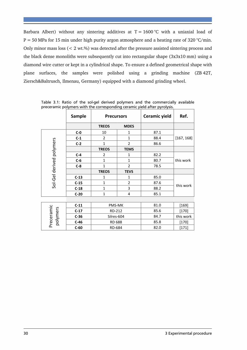
30 3 Experimental procedure
Barbara Albert) without any sintering additives at T = 1600 °C with a uniaxial load of
P = 50 MPa for 15 min under high purity argon atmosphere and a heating rate of 320 °C/min.
Only minor mass loss (< 2 wt.%) was detected after the pressure assisted sintering process and
the black dense monoliths were subsequently cut into rectangular shape (3x3x10 mm) using a
diamond wire cutter or kept in a cylindrical shape. To ensure a defined geometrical shape with
plane surfaces, the samples were polished using a grinding machine (ZB 42T,
Ziersch&Baltrusch, Ilmenau, Germany) equipped with a diamond grinding wheel.
Table 3.1: Ratio of the sol-gel derived polymers and the commercially available preceramic polymers with the corresponding ceramic yield after pyrolysis.
Sample Precursors Ceramic yield Ref.
TREOS MDES
Sol-
Gel
der
ived
po
lym
ers
C-0 10 1 87.1
[167, 168] C-1 2 1 88.4
C-2 1 2 86.6
TREOS TEMS
C-4 2 1 82.2
this work C-6 1 1 80.7
C-8 1 2 78.5
TREOS TEVS
C-13 1 1 85.0
this work C-15 1 2 87.6
C-18 1 3 88.2
C-20 1 4 85.1
Pre
cera
mic
p
oly
me
rs C-11 PMS-MK 81.0 [169]
C-17 RD-212 85.6 [170]
C-36 Silres-604 84.7 this work
C-46 RD 688 85.8 [170]
C-60 RD-684 82.0 [171]

4 Experimental procedure 31
Figure 3.1: Schematic depiction of the sol-gel precursors and the preceramic polymers.
3.2 Materials characterization
The following chapter presents the equipment used for the structural and compositional
characterization of the ceramic.
3.2.1 Elemental analysis
The elemental composition of the samples was determined by hot gas extraction. The carbon
content of the samples was measured with a carbon analyzer (CS 800, Eltra GmbH, Neuss,
Germany) which detects and quantifies the oxidized carbon species by means of IR
spectroscopy. An N/O analyzer (Leco TC-436, Leco Corporation, Michigan, US) was used to
determine the oxygen content. A similar measurement principle is being used to analyze the
oxygen content as the present oxygen of the sample reacts with the graphitic crucible to form
CO2. The escaping CO2 can be quantified through IR spectroscopy. The silicon weight fraction
was considered to be the difference to 100 wt.%, assuming no other elements being present in
the sample.

32 3 Experimental procedure
3.2.2 Density and porosity measurements
The bulk density of the obtained ceramics was determined by the Archimedes method, using
distilled water as infiltration medium. Hereby, the sample volume VF is calculated by the
difference between the weight of the dry sample (md) in air and submerged in water (mn,H2O)
divided by the density of water ρH2O. Accordingly, the volume of the sample VS reads:
𝑉𝑆 =𝑚𝑑 − 𝑚𝑛,𝐻2𝑂
𝜌𝐻2𝑂 (3.1)
Afterwards, the soaked up sample (mn,air) is weighted in air and its mass is subtracted from the
weight of the dried sample (md) providing the volume of the open pores VP.
𝑉𝑃 =𝑚𝑛,𝑎𝑖𝑟 − 𝑚𝑑
𝜌𝐻2𝑂 (3.2)
The percentage share of the open porosity is calculated by dividing the volume of the pores VP
by the geometrical volume VS:
𝑃𝑜𝑝𝑒𝑛 = 100 ∙𝑉𝑃
𝑉𝑆 (3.3)
This method only provides access to open pores which can be infiltrated by water. The overall
density of the sintered ceramic is calculated according to:
𝜌 =𝑚𝑑 − 𝜌𝐻2𝑂
𝑚𝑛,𝑎𝑖𝑟 − 𝑚𝑛,𝐻2𝑂 (3.4)
3.2.3 Raman spectroscopy
A tunable Ti:sapphire solid state laser (Coherent, Indigo-S) with an excitation wavelength of
λ = 256.7 nm (i.e., 4.8 eV) was employed for the UV Raman studies. Anisotropic BBO (β-barium
borate) and LBO (lithium triborate) crystals have been used to generate the UV radiation by
frequency tripling the fundamental (λ = 770.1 nm) of the laser. Scattered radiation is dispersed
and detected with a triple stage spectrometer (Princeton Instruments, TriVista 555) equipped
with a CCD camera (Princeton Instruments, Spec10:2kBUV). The spectral resolution of the
spectrometer is µ ≈ 1cm-1. A mirror system has been designed to guarantee an efficient collection
of the scattered Raman photons. A spherical mirror (Edmund Optics) focuses the laser beam
onto the sample. Two 90° off-axis parabolic mirrors (Thorlabs) collect and refocus the scattered
photons into the spectrometer. Prior to each measurement, the spectrometer has been
calibrated using boron nitride and the laser power was reduced to ≤ 400 µW to avoid sample
damage. The acquisition time of each spectrum was ≥ 1h to obtain a signal-to-noise ratio ≥ 3.

4 Experimental procedure 33
Visible Raman spectra were recorded with a Horiba HR800 micro-Raman spectrometer (Horiba
Jobin Yvon GmbH, Bensheim, Germany) equipped with an Argon laser (λ = 514.5 nm). The
excitation line has its own interference filter (to filter out the plasma emission) and a Raman
notch filter (for laser light rejection). The measurements were performed with a grating of 600
and a confocal microscope (magnification 50x, NA = 0.5) with a 100 μm aperture, giving a
resolution of approximately 2 μm – 4 μm. The laser power (20 mW) was attenuated by using
neutral density filters; thus the power on the sample was in the range from 6 μW to 2 mW. All
spectra were background subtracted, smoothed (SMA, simple moving average) and fitted to
Lorentzian line shapes using Origin Pro 9.1.0G.
3.2.4 Thermogravimetric analysis
Thermogravimetric analysis (TGA) was performed with a STA 449C Jupiter (Netzsch Gerätebau
GmbH, Hanau, Germany) coupled to a FT-IR-spectrometer (Tensor27, Bruker, Massachusetts,
USA). The TGA was conducted in order to investigate the thermal stability of SiOC/C in
oxidizing atmosphere by measuring the mass change as well as the evolution of carbon
monoxide and carbon dioxide. The analysis was performed under a constant oxygen gas flow
(Air Liquide, purity ≥ 99.5 %) and argon gas flow (Air Liquide, purity ≥ 99.5 %) of 30 ml/L.
100 mg of the ceramic powder were placed into a Al2O3 crucible for the measurement.
Temperature steps at T = 200, 400 and 600 °C were set with a heating rate of 5 °C/min and a
holding time of 2 h before the measurement temperature was increased to T = 800 °C and
1000 °C with a reduced dwelling time of 1 h. The outgasing species were recorded with an FT-
IR spectrometer in a range from 500 to 4000 cm-1. The mass change of the sample was recorded
with 100 points per minute during the heating ramp and 4 points per minute during the
dwelling.
3.2.5 X-ray diffraction
The diffraction pattern were either preformed in flat-sample transmission geometry on a STOE
STAD1 P diffractometer (STOE & Cia GmBH, Darmstadt, Germany) equipped with
monochromatic Mo-Kα ( = 0.07093 nm) radiation for powdered samples or on a STOE X-ray
diffractometer using Ni-filtered Cu-Kα ( = 0.15405 nm) radiation in case of bulk samples. Both
devices are located at the Technical University of Darmstadt in the working group of Prof.
Wolfgang Donner. Isoamylacetate was used to fix the powdered samples between two acetate
foils for the measurement at the STOE STAD1 P.
34 3 Experimental procedure
3.2.6 X-ray photoelectron spectroscopy
The measurement were conducted at the Technical University of Darmstadt in the working
group of Prof. Wolfram Jägermann using a PHI VersaProbe 5000 spectrometer (Physical
Electronics Inc. MN, USA) equipped with a monochromatic Al-Kα source (hν = 1486.6 eV) with
a beam diameter of 200 µm. The binding energies are referred to the Fermi level of Ag foil.
Photoelectrons were collected with the pass energy, Epass = 23.5 eV at θ = 45° with respect to
the surface normal. The background under the high resolution XPS spectra was subtracted by a
Shirley-type function using the software XPSPEAK 4.1.
3.2.7 Scanning Electron Microscope
Scanning electron microscopy (SEM) pictures were performed on a Philips XL30 FEG (Philips,
Netherlands) by detecting low-energy secondary electrons emitted from the surface
(10 - 100 nm) due to excitation by the primary high-energy electron beam. Low conductive
samples were coated with a thin layer of gold using an EMITECH K950X (Quorum Technilogies
Ltd, Kent, UK) in order to avoid charging effects on the sample surface. Imaging was performed
at an acceleration voltage of 10 to 25 kV with a secondary electron detector. Semi-quantitative
elemental analysis is also possible using energy dispersive X-ray (EDX) module (CDU, EDAX
Inc.) via detection of the characteristic X-rays excited by the incident electron beam.
3.3 Electrical investigations
In this chapter the electrode application of the different sample geometries is described together
with the experimental setup up used to determine their electronical properties. Furthermore,
the developed setup to characterize the piezoresistive behavior is presented.
3.3.1 Electrical contacting of the samples
To ensure a good electrical contact and to minimize the contact resistance, on both sample
geometries a thin layer (≈ 70 nm) of Au or Pt was sputtered using a EMITECH K950X (Quorum
Technilogies Ltd, Kent, UK) for 8 min at 40 mA. The cylindrical samples were sputtered on the
front side whereas the electrodes of the rectangular samples are located at the long side, as they
had to be excluded from the strain direction applied during the piezoresistive measurements.
Gold wires (d = 0.5 mm) were attached onto the sputtered electrodes in case of the rectangular
shaped samples using a gold paste (Gwent group, Pontypool, UK). The paste is burned at
T = 700 °C in an alumina tube furnace for 1 h under a flowing stream of high purity argon to
promote the conductivity and adhesion. The oven chamber is evacuated three times and flushed

4 Experimental procedure 35
with argon to avoid any oxidation reaction. Subsequently, to prevent oxidation during the
measurement the electronic contacts are sealed using an Al2O3-based glue (Thermokitt 1100°C,
Carl Roth GmbH & Co. KG, Karlsruhe, Germany) by simply drying at T = 100 °C for 12 h. No
change in resistance was observed when the resistance was measured with a four-point method
allowing to neglect the contact resistance. Both contacting methods are depicted in Figure 3.2.
Figure 3.2: Schematic depiction of two different samples geometries with a) the rectangular and b) the
cylindrical shape used during the electrical investigations.
3.3.2 Temperature dependent impedance spectroscopy
The impedance spectroscopy offers the possibility to investigate the electrical properties under
an alternating current. The device is located at the Technical University of Darmstadt in the
working group of Prof. Jürgen Rödel. In the course of the electrical examination the cylindrical
samples are clamped between two electrodes (two-point method) within a quartz tube and
subsequently hermetically sealed before the tube was slid into a cylindrical alumina furnace
(LOBA 1400-45-400-1, HTM Reetz GmbH, Berlin, Germany). Temperatures up to T = 800 °C
are available and are verified by a thermocouple placed next to the sample. The tube is
evacuated und flushed with argon (Air Liquide, purity ≥ 99.5 %) three times before the heating
program is started. For electrical investigation an Alpha-A High Performance Modular
Measurement System (Novocontrol Technologoies, Montabaur, Germany) is used. The
measurements are conducted within a frequency range of ν = 0.1 to 3 MHz and an applied
voltage of U = 0.1 V.
3.3.3 Piezoresistive measuring chamber
Within this work, a specially developed experimental setup was constructed in cooperation with
the Electromechanical Department (EMK) at the TU Darmstadt to assess the static
piezoresisitive behavior of SiOC/C ceramics. The complete setup and the measurement chamber
are depicted in Figure 3.3. The rectangular polished samples were clamped between to two
plane alumina rods (Ø = 5 mm) and preloaded with P = 10 MPa for 30 min. The mechanical
load is applied by a stepper motor with a rating of F = 1000 N and regulated by a load cell
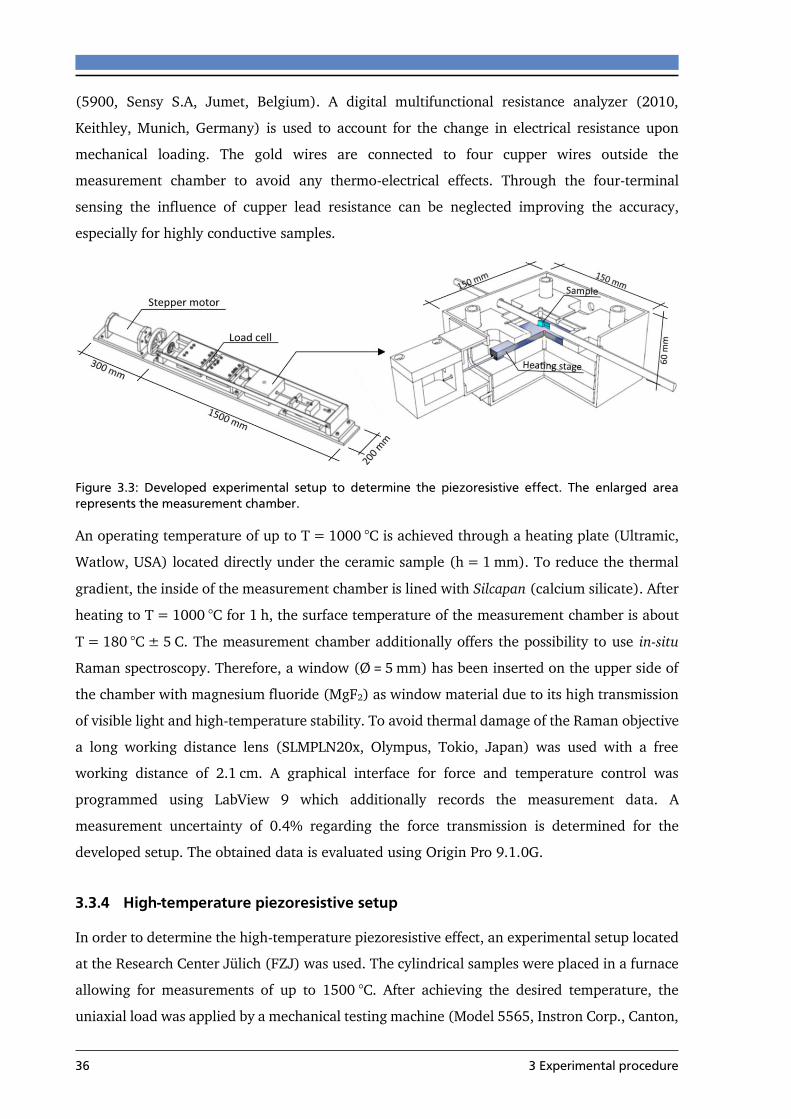
36 3 Experimental procedure
(5900, Sensy S.A, Jumet, Belgium). A digital multifunctional resistance analyzer (2010,
Keithley, Munich, Germany) is used to account for the change in electrical resistance upon
mechanical loading. The gold wires are connected to four cupper wires outside the
measurement chamber to avoid any thermo-electrical effects. Through the four-terminal
sensing the influence of cupper lead resistance can be neglected improving the accuracy,
especially for highly conductive samples.
Figure 3.3: Developed experimental setup to determine the piezoresistive effect. The enlarged area
represents the measurement chamber.
An operating temperature of up to T = 1000 °C is achieved through a heating plate (Ultramic,
Watlow, USA) located directly under the ceramic sample (h = 1 mm). To reduce the thermal
gradient, the inside of the measurement chamber is lined with Silcapan (calcium silicate). After
heating to T = 1000 °C for 1 h, the surface temperature of the measurement chamber is about
T = 180 °C ± 5 C. The measurement chamber additionally offers the possibility to use in-situ
Raman spectroscopy. Therefore, a window (Ø = 5 mm) has been inserted on the upper side of
the chamber with magnesium fluoride (MgF2) as window material due to its high transmission
of visible light and high-temperature stability. To avoid thermal damage of the Raman objective
a long working distance lens (SLMPLN20x, Olympus, Tokio, Japan) was used with a free
working distance of 2.1 cm. A graphical interface for force and temperature control was
programmed using LabView 9 which additionally records the measurement data. A
measurement uncertainty of 0.4% regarding the force transmission is determined for the
developed setup. The obtained data is evaluated using Origin Pro 9.1.0G.
3.3.4 High-temperature piezoresistive setup
In order to determine the high-temperature piezoresistive effect, an experimental setup located
at the Research Center Jülich (FZJ) was used. The cylindrical samples were placed in a furnace
allowing for measurements of up to 1500 °C. After achieving the desired temperature, the
uniaxial load was applied by a mechanical testing machine (Model 5565, Instron Corp., Canton,

4 Experimental procedure 37
MA, USA) using alumina rods as extensions. Two platinum electrodes were used for electronic
contacting. To ensure a low contact resistance and to exclude any pressure induced changes in
resistance, the electrodes were preloaded with P = 3 MPa. The resistivities of the loaded and
unloaded samples, respectively, were calculated from the observed voltage changes using a
multifunctional resistance analyzer (2010, Keithley, Munich, Germany).
3.3.5 Hall measurements
Hall measurements were conducted to measure the electrical conductivity, the Hall constant,
carrier mobility and carrier density of the bulk ceramic by the means of an IMP-HT-Hall-900K
system (Frauenhofer IPM, Freiburg, Germany) at the University of Mainz. Square-shaped
samples (1x10x10 mm) are placed into a sample holder installed within a vacuum chamber. To
reduce measurements uncertainties, only samples with parallel main surfaces are used. The
chamber is subsequently evacuated and flushed with argon (Air liquid, purity 99.5%). To
measure the specific electrical conductivity, the sample is contacted according to the
van-der-Pauw measurement theory. Thus, four points are connected at the edge of the sample
whereas on one side of the sample the current is applied and on the other side the resulting
voltage is measured. The separation of the current and voltage electrode eliminates the contact
and lead resistance from the measurement and thereby increases the accuracy. The
measurement is done in all four permutations of the contacts, and due to the used AC-resistance
bridge in both polarisations. The vacuum chamber moves into positive and negative field
position to determine the Hall coefficient and carrier concentration and mobility.

38 4 Results and discussion
4 Results and discussion
In chapter 4.1 the material properties of SiOC/C are discussed in detail followed by the Raman
study of the carbon phase in chapter 4.2. In the following two chapters 4.3 and 4.4 the electrical
and piezoresistive properties of SiOC/C are reported which ultimately lead to a development of
a preliminary sensor prototype.
4.1 Structural characterization and thermal stability of SiOC/C
This chapter delivers a short survey over the various synthesized silicon oxycarbides (SiOC/C)
and how the sintering parameters have to be adjusted in order to ensure a dense bulk ceramic.
Density and porosity measurements were preformed to follow the densification process. The
related change in microstructure and crystallinity is investigated through XRD and XPS
measurements. Finally, the thermal stability of the ceramic is investigated by the means of TGA-
FTIR measurements up to T = 1000 °C.
4.1.1 Phase composition
In general, SiOC/C glasses can easily be prepared through a direct polymer-to-ceramic
transition by pyrolysis of cross-linked poly-organosiloxane networks. These networks contain
Si-R bonds (R = H, CH3, CH2CH3, C6H5, …) and can be produced from monomeric
organosiloxanes precursors using the sol-gel process and preceramic polymers. A schematical
depiction of the sol-gel process and the development of a sol-gel-derived organosiloxane
network is illustrated in Figure 4.1.
Figure 4.1: Schematically depiction of the sol-gel process and the derived organosiloxane network.
In the present work, either triethoxyvinylsilane (TEVS) or triethoxymethylsilane (TEMS) where
mixed with triethoxysilane (TREOS) in different ratios to tailor the chemical composition,
notably the amount of residual carbon within the microstructure after pyrolysis. The latter

4 Results and discussion 39
precursor ensures the establishment of a well-connected network, to lower the mass loss during
the pyrolysis step, while the first precursors incorporate carbon into the organosiloxane
network. The large range of composites synthesized are presented in the teneray Si-O-C phase
diagram displayed in Figure 4.2.
The majority of samples were prepared at T = 1600 °C and mainly consist of SiO2, SiC and C
[32]. Most of the compositions synthesised during this work (represented by the green dots)
are located in the SiO2-rich area and exhibit a linear change in composition with increasing
amount of carbon. Some of the commercially obtained poly-organosiloxanes (represented by
the red dots) deviate from the linear dependency which is due to their different chemical
functionalization and/or crosslinking situation in the initial polymeric stage. The connecting
line between SiC and SiO2 represents compositions in which all carbon is bonded to silicon and
no excess carbon is present. Compositions above that line, inside the SiC-SiO2-Si triangle lead
to the presence of elemental silicon. However, the vast majority of reported SiOC/C glasses
studied so far usually contain excess carbon and their composition falls inside the SiO2-SiC-C
triangle following the expression SiCxO2(1-x)+Cy.
Figure 4.2: Si-O-C phase diagram including the compositions of silicon oxycarbide ceramics pyrolysed at
T = 1600 °C. The green dots represent synthesised compositions, while the red dots are derived from
commercially available perceramic polymers.
Two assumptions are required to calculate the amount of excess carbon from the elemental
analysis. The first premise is that oxygen is strictly bonded to silicon and that no carbon-oxygen
bonds are present in the ceramic [172]. In addition, if the materials are fired at temperatures
T > 1000 °C the hydrogen content is below 1 wt.% and can be neglected [173]. Assuming a
density of ρ = 1.45 g/cm³ for the segregated carbon [174] and a density value of ρ = 2.3 g/cm³

40 4 Results and discussion
for the amorphous SiOxCy network [172] the volume fraction of the carbon phase C can be
calculated according to:
𝜙𝑐 =[𝑦 − (1 −
𝑥
2)]∙𝑀𝐶/𝜌𝐶
1∙𝑀𝑆𝑖+𝑥∙𝑀𝑂+𝑦∙𝑀𝐶/𝜌𝑆𝑖𝑂𝑥𝐶𝑦 (4.1)
When the preparation temperature exceeds T > 1300 °C, phase separation of the amorphous
network and ordering of the segregated carbon occurs. Therefore, the density of segregated
carbon may increase up to ρ = 1.82 g/cm³ [175], while the overall density of the ceramic is
mainly determined by the resulting components SiO2 (2.33 g/cm³)[176] and SiC
(3.21 g/cm³)[177]. Thus, in a phase separated system, the volume fraction of the segregated
carbon phase is given by:
𝜙𝑐 =[𝑦 − (1 −
𝑥
2)]∙𝑀𝐶/𝜌𝐶
[𝑦 − (1 − 𝑥
2)]∙𝑀𝐶/𝜌𝐶+(
𝑥
2∙𝑀𝑆𝑖𝑂2/𝜌𝑆𝑖𝑂2)+(1 −
𝑥
2 −
3𝑧
4∙𝑀𝑆𝑖𝐶/𝜌𝑆𝑖𝐶)
(4.2)
A brief summary of selected compositions heat treated at T = 1600 °C is presented in the
following Table 4.1. The SiOC/C samples are labelled according to their volume fraction of
excess carbon. Hence a sample with a volume fraction of C = 11 vol. % of segregated carbon is
designated as C-11.
Table 4.1: Elemental analysis of selected samples after pyrolysis at T = 1600 °C for 15 min in Argon.
Sample weight percent fraction SiOC/C
empirical formula
volume percent fraction
Si O C SiO2 SiC C
C-1 50.97 42.14 6.89 SiO1.45C0.28 + 0.04C 84.27 14.55 1.18
C-8 48.38 38.69 12.93 SiO1.42C0.29 + 0.31C 77.42 14.38 8.20
C-11 46.65 39.40 13.95 SiO1.48C0.26 + 0.44C 76.75 12.24 11.01
C-17 49.13 26.44 24.43 SiO0.94C0.53 + 0.63C 54.49 27.83 17.68
C-36 36.53 27.90 35.57 SiO1.34C0.33 + 1.95C 51.91 11.66 36.43
From Table 4.1, a linear decrease of the SiO2 phase can be identified as the amount of carbon
is raised and incorporated into the microstructure. The same trend is found in Figure 4.3 which
summarizes the evolution of the SiO2 and SiC phase as a function of the carbon volume fraction
for all samples synthesized during this work. All samples shown have been prepared under the
same conditions (T = 1600 °C; P = 50 MPa).
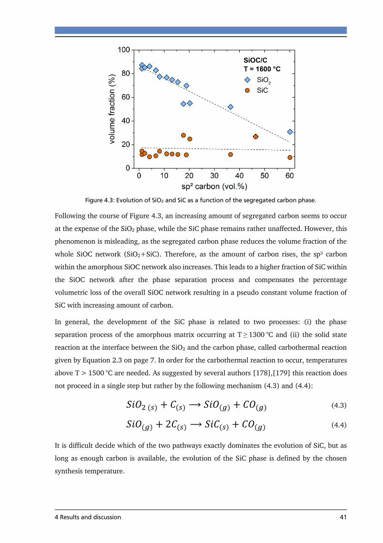
4 Results and discussion 41
Figure 4.3: Evolution of SiO2 and SiC as a function of the segregated carbon phase.
Following the course of Figure 4.3, an increasing amount of segregated carbon seems to occur
at the expense of the SiO2 phase, while the SiC phase remains rather unaffected. However, this
phenomenon is misleading, as the segregated carbon phase reduces the volume fraction of the
whole SiOC network (SiO2+SiC). Therefore, as the amount of carbon rises, the sp³ carbon
within the amorphous SiOC network also increases. This leads to a higher fraction of SiC within
the SiOC network after the phase separation process and compensates the percentage
volumetric loss of the overall SiOC network resulting in a pseudo constant volume fraction of
SiC with increasing amount of carbon.
In general, the development of the SiC phase is related to two processes: (i) the phase
separation process of the amorphous matrix occurring at T ≥ 1300 °C and (ii) the solid state
reaction at the interface between the SiO2 and the carbon phase, called carbothermal reaction
given by Equation 2.3 on page 7. In order for the carbothermal reaction to occur, temperatures
above T > 1500 °C are needed. As suggested by several authors [178],[179] this reaction does
not proceed in a single step but rather by the following mechanism (4.3) and (4.4):
𝑆𝑖𝑂2 (𝑠) + 𝐶(𝑠) ⟶ 𝑆𝑖𝑂(𝑔) + 𝐶𝑂(𝑔) (4.3)
𝑆𝑖𝑂(𝑔) + 2𝐶(𝑠) ⟶ 𝑆𝑖𝐶(𝑠) + 𝐶𝑂(𝑔) (4.4)
It is difficult decide which of the two pathways exactly dominates the evolution of SiC, but as
long as enough carbon is available, the evolution of the SiC phase is defined by the chosen
synthesis temperature.

42 4 Results and discussion
4.1.2 Densification process
Figure 4.4 a) displays the densities of sample C-11 and C-17 as a function of the thermal
treatment between 1000 °C < T < 1800 °C. No densification could be achieved at temperatures
below T ≤ 1000 °C as only highly porous samples, not able to retain their shape, were obtained.
The density of both samples progress in a comparable manner with increasing pyrolysis
temperature in the range of ρ = 2.2 - 2.3 g/cm³ with C-17 having a slightly greater density.
Upon further annealing at temperatures above T > 1600 °C the density of C-17 increases up to
ρ = 2.75 g/cm³, while the density of C-11 only slightly increases up to ρ = 2.38 g/cm³. The
strong increase in density of C-17 can be explained in terms of the higher amount of segregated
carbon and the thermally promoted carbothermal reaction which converts the silica phase into
silicon carbide. The obtained density of C-17 at T = 1800 °C is in accordance with the literature-
known values of amorphous silicon carbide [180].
Figure 4.4: Density and residual open porosity of C-11 and C-17 heat treated at various temperatures.
The porosities of both samples (C-11 and C-17) is depicted in Figure 4.4 b). In both cases an
open porosity of Φ ≈ 40 % is obtained when the samples are prepared at T = 1000 °C. Increasing
the temperature up to T = 1600 °C under a constant pressure constantly reduces the porosity
down to Φ = 0.1 % for C-11 and Φ = 1.1 % for C-17. Further annealing up to T = 1800 °C
causes the porosity of both samples to slightly increase as the carbothermal reaction gain in
significance causing decomposition of the sample. To avoid any decomposition reactions, yet to
ensure a dense microstructure, which is essential for a reproducible piezoresistive effect, the
synthesis temperature was set to T = 1600 °C with a holding time of 15 min and a pressure of
P = 50 MPa. In addition, graphite sealing foils and graphite dies were used during the synthesis
to separate the ceramic powder from the punch and furthermore to supress the carbothermal

4 Results and discussion 43
reaction. It was found that the chemical composition of the sample remains constant regardless
if the applied heat treatment is raised. This is emphasized in Table 4.2 and proves that the
carbothermal reaction is supressed in C-11 under the given circumstances [181].
Table 4.2: Elemental analysis of sample C-11 pyrolysed at temperatures between T = 1000 – 1800 °C.
Temp. weight percent SiOC/C
empirical formula
volume percent
Si O C SiO2 SiC C
1000 °C 47.27 38.71 14.02 SiO1.44C0.28 + 0.41C 75.91a 13.56a 10.53
1200 °C 46.56 39.02 14.42 SiO1.47C0.26 + 0.46C 76.03a 12.48a 11.49
1400 °C 45.88 39.65 14.47 SiO1.52C0.24 + 0.50C 76.72 11.16 12.12
1600 °C 46.65 39.40 13.95 SiO1.48C0.26 + 0.44C 76.75 12.24 11.01
1800 °C 46.89 38.70 14.41 SiO1.45C0.28 + 0.44C 75.67 13.15 11.18
a= formal chemical composition of the amorphous SiOC network.
Figure 4.5 displays SiOC/C samples with various carbon content all prepared under the same
conditions (T = 1600 °C, P = 50 MPa, t = 15 min). The SEM images reveal that only samples
up to a carbon volume fraction of C = 17 vol.% can be densified (Φ < 1%) under the given
parameters.
Figure 4.5: SEM images of different SiOC/C samples prepared at T = 1600 °C under P = 50 MPa.
Higher carbon concentrations lead to silica domains fully encapsulated by a thin layer of carbon
which act as a diffusion barrier and thus hinders the viscous flow and densification process of
the SiOC/C system [37, 153]. Furthermore, partial decomposition may take place at
temperatures above T > 1400 °C which retards the densification process due to gas formation
[182]. However, this can be excluded due to a rather small equilibrium rate constant of
Kp = 0.072 for the carbothermal reaction at T = 1430 °C. According to the thermodynamic
calculations of Plachký et al., a CO pressure of pCO = 0.07 bar is necessary to supress the

44 4 Results and discussion
carbothermal reaction at T = 1600 °C. Through the usage of graphite sealing foils the partial
pressure of CO at the vicinity of the sample surface is assumed to be sufficiently high enough
to shift the equilibrium supressing the carbothermal reaction during synthesis [181]. Hence,
the preparation and densification of SiOC/C bulk ceramics is thermally restricted by the
carbothermal reaction due to the decomposition of the material and by the amount of
segregated carbon limiting the densification process.
4.1.3 Crystallization and bonding situation
To investigate the crystallization behavior of SiOC/C and to clarify if the amount of excess
carbon does have an influence on the crystallization behavior, X-ray diffraction were performed.
The XRD pattern of C-17, C-11 and C-1 heat treated at temperatures from T = 1200 to 1800 °C
with a holding time of 15 min are given in Figure 4.6.
Figure 4.6: XRD patterns of C-17, C-11 and C-1 synthesized at temperatures between 1200 - 1800 °C.
The sample C-11 prepared at T = 1200 °C was found to be X-ray amorphous with a broad halo
around 2ϴ = 22° corresponding to a disordered silica structure [35]. Upon further annealing,
broad and weak signals of β-SiC emerge, which gain in intensity and shape until the final
temperature of T = 1800 °C is reached. The crystallization of SiC is represented by the major
reflexes at 2ϴ = 35° and 60° corresponding to the (111) and (101) β-SiC lattice planes. A similar
crystallization pathway is found for the C-17 sample with the difference that the key signatures
of β-SiC already appear at T = 1200 °C and that the crystalline reflexes at the highest
temperature reading T = 1800 °C clearly display a higher fraction of crystallinity. The small
shoulder at 2ϴ = 33.5° appears due to stacking faults in β-SiC. Considering the amorphous
nature and neglecting the internal strain within the precipitation the β-SiC particle size can be
4 Results and discussion 45
roughly estimated according to the Scherrer equation. Hence, when the temperature is raised
from T = 1600 °C to 1800 °C, the crystallite size of SiC within C-11 increased from 2.5 to
6.8 nm. In case of C-17, the crystalline size grew by the factor of 10 from 3.0 to 32.2 nm.
HR-TEM investigations support these findings, revealing that the β-SiC crystallite size is about
2 - 4 nm when treated at T = 1600 °C. In addition, the measurements suggest that the majority
is located in close proximity to the edges of carbon segregations [36, 37]. The carbon atoms at
the edges are expected to be less stable at elevated temperatures and thus are being assumed
to be the nuclei of further SiC crystal growth [183]. Although, diffuse reflexes of SiC are already
obtained at T = 1200 °C, it remains an open question if the origin of initial β-SiC precipitations
is due to reorganization of the amorphous SiOC phase and the subsequent carbothermal
reaction or either due to decomposition of the amorphous SiCO microstructure directly leading
to β-SiC [32]. The relatively weak reflex at 2ϴ = 26.7° is related to carbon segregations within
the SiOC microstructure and is associated to graphitic in-plane structures [171]. The XRD
pattern of C-1 showed no reflexes at all being completely amorphous up to T = 1600 °C. This is
rather interesting as one would expect, that due to the low amount of carbon the formation of
cristobalite should not be obstructed.
Nevertheless, no signs of cristobalite, which is usually formed in vitreous silica at temperatures
exceeding T > 1200 °C, are found in the XRD pattern. A possible reason is the phase separation
process of the amorphous network as long as the separation distance of the SiO2 and SiC
domains is less than 1.0 nm. The low distance between the separated domains might be in fact
too small for nucleation to occur [36]. Saha and Raj assumed a low interfacial energy between
SiC and SiO2 as a possible reason for this phenomenon [32]. Moreover, the segregated carbon
phase may obstruct long-range diffusion of silica cluster, not allowing the formation of small
clusters required to nucleate cristobalite.
The important role of the segregated carbon phase in terms of the crystallization behavior have
been pointed out by many researches [172, 184, 185]. According to Sousa et al. [186], carbon-
rich SiOC leads to larger SiC crystals but when decreasing the carbon concentration, smaller
SiC crystallites are obtained and cristobalite starts to crystallize. In this study, similar findings
regarding the crystallization behavior of SiC have been found but no signs of cristobalite were
discovered suggesting that the carbon concentration is still high enough to obstruct the
crystallization even in carbon depleted samples. The absence of cristobalite and the diffuse XRD
reflexes together with the nano-sized β-SiC precipitates indicates that these materials exhibit
an outstanding resistance against crystallization in the range of T ≤ 1600 °C. This phenomenon
is assumed to rely on the segregated carbon phase distributed throughout the whole SiOC
microstructure. However, as soon as the temperature is raised above T = 1600 °C, the

46 4 Results and discussion
carbothermal reaction becomes an increasingly important parameter promoting the
crystallization of β-SiC under decomposition of the SiOC/C ceramic.
To gain further insight into the different types of bonds and their distribution within the SiOC
matrix, high resolution XPS and MAS-NMR techniques are commonly used, due to their high
sensitivity to the chemical surrounding of silicon atoms. Five combinations of mixed silicon
tetrahedra may be present in a SiOC matrix, schematically depicted in Figure 4.7. Several
studies addressing the distribution of these units were performed using MAS-NMR technique.
They could show that, below T < 1300 °C the amorphous SiOC matrix consist of all five silicon
tetrahedral units, but is mostly divided into oxygen-rich and carbon-rich domains [31, 33].
Figure 4.7: A schematic of the five mixed silicon tetrahedra units found in silicon oxycarbide materials.
Above T > 1300 °C, the majority of the mixed tetrahedra diminishes and in general transforms
into SiC4 and SiO4 units [37, 167]. The XPS technique is a typical surface technique (5 - 7 nm)
that delivers valuable information about the different bonding situations. However, it should
be noted here, that in amorphous materials where variations in bond length and angle causes
broadening of peaks which lead to uncertainties in quantifying species with almost identical
chemical shift, such as the mentioned mixed silicon-tetrahedra.
For SiO2 and SiC, the Si(2p) electrons exhibit binding energies of 103.0 eV and 100.1 eV,
respectively. The Si(2p) spectrum obtained from C-1, C-11 and C-17 (all densified at
T = 1600 °C and P = 50 MPa) are displayed in Figure 4.8 showing a broad cumulative peak
with a small shoulder at lower binding energies. The peak spans over the typical binding
energies of SiO2 and SiC suggesting the presence of mixed silicon tetrahedra [187, 188]. The
largest area in all samples is governed by the Si-O bonding signal at 103.3 eV corresponding to
a silica near structure. The peak at 100.5 eV is assigned to Si-C bonds closely related to SiC
structures. Due to the amorphous nature of the ceramic and the nearly identical binding
energies of the mixed units, no appropriate distinction between them could be drawn. In case
of C-1, the peak is located around 101.7 eV and slightly shifts towards higher binding energies
(102.0 eV) with increasing amount of carbon.

4 Results and discussion 47
Figure 4.8: Experimental Si(2p) spectrum for C-1, C-11 and C-17 all prepared at T = 1600 °C.
The fact that even after the highest temperature treatment (T = 1600 °C) fully-phase separated
SiOC/C still contains mixed tetrahedra is quite surprising as MAS-NMR studies suggest only the
presence of SiO2 and SiC. However, the existence of mixed tetrahedra in phase-separated SiOC
has been already proposed in the past and are assumed to be located at the interface between
the SiC nanoparticles and the silica matrix [36, 189].
The XPS C(s1) spectrum presented in Figure 4.9 suggests the presence of three components at
282.9, 284.4 and 286.4 – 286.7 eV. The peak located at 282.9 eV is assigned to Si-C bonds
whereas the second peak at 284.4 eV is due to aromatic C-C bonds. Both peaks increase in area
as the amount of carbon is raised from C-1 to C-17.
Figure 4.9: Experimental C(1s) spectrum for C-1, C-11 and C-17 all prepared at T = 1600 °C.

48 4 Results and discussion
The assignment of the last peak in range of 286.4 - 286.7 eV is uncertain. As the XPS technique
is a surface sensitive technique, the C-O peak might be assigned to a surface oxidation. Another
possibility involves the carbothermal reaction and may consider C-O bonds as an intermediate
stage during the commencing reduction of the SiO2 network [188].
Figure 4.10 presents the O(1s) XPS spectrum showing three types of oxygen bonds located
between 530.7 - 531.3, 532.0 - 532.2 and 533.0 - 533.3 eV. The latter peak is assigned to Si-O
bonds of silica-near structures and is greatest for C-1. Increasing the amount of carbon causes
the peak to decrease which is in agreement with the accompanied decline of the SiO2 phase. No
clear differentiation between the mixed silicon units, represented by the peaks between
532.0 – 532.2 eV, could be made. The last peak at 531.0 eV can be assigned to C-O. In case of
the C-17 sample, the peak shifts to binding energies of about 530 eV making it difficult to
designate a certain bond.
Figure 4.10: Experimental O(1s) spectrum for C-1, C-11 and C-17 all prepared at T = 1600 °C.
In summary, the XPS technique provides valuable information about the binding situation in
SiOC/C revealing the presence of mixed silicon units even at synthesis temperatures up to
T = 1600 °C. Nevertheless, a profound knowledge about the bonding situation will only be
gained with the help of other techniques such as the MAS-NMR [31, 190]. However, further
MAS-NMR and XPS studies are needed to support the presented data, especially as XPS is a
surface sensitive technique.

4 Results and discussion 49
4.1.4 Impact of oxidation on the electrical conductivity
Little attention has been paid to the temporary stability of the electrical properties of silicon
oxycarbide materials in literature so far [191], although it represents a sensitive measure of its
oxidation behavior. Therefore, this chapter examines the electrical conductivity under oxidizing
atmospheres to determine the potential usage of SiOC/C as a sensor material at elevated
temperatures.
Figure 4.11 depicts the electrical resistivity of a C-17 sample heated at T = 200 °C, 400 °C and
500 °C in air with a dwelling time of 1 h. The resistivity decreases with increasing temperature
suggesting activated transport and remains constant at the dwelling times. Degradation of
SiOC/C is obviously not relevant up to temperatures of T = 500 °C and the temporary stability
of the electrical signal is sufficient for the intended sensor development, see chapter 4.4.5.
However, other sensor applications may require a better long-term stability of the electrical
signal and a more comprehensive study should be carried out.
Figure 4.11: The course of the electrical resistivity of C-17 heated up to T = 500 °C in air.
The degradation of SiOC/C has been also checked by thermo-chemical measurements. Figure
4.12 shows the thermogravimetric analysis coupled with Fourier Transform Infrared
Spectroscopy (TGA-FTIR) of C-11 and C-17 heated up to T = 1000 °C in air.

50 4 Results and discussion
Figure 4.12: TGA-FTIR spectrum of a) C-11 and b) C-17 in the temperature range of 25 – 1000 °C.
A very small mass gain of 0.05 wt.% accompanied by a weak CO2 signal is detected for C-11 up
to T = 1000 °C. A comparable mass gain is obtained for C-17 but only up to a temperature of
T = 600 °C. At higher temperatures a steep mass decrease of 1.5 wt.% occurs at about
T = 800 °C. If the temperature is further raised up to at T > 900 °C the mass increases again by
about 1.1 wt.%. The changes in mass are accompanied by the respective changes of the CO2
signal and may be explained by the following reactions [191, 192]:
𝐶 + 𝑂2 → 𝐶𝑂2(𝑔) (4.5)
𝑆𝑖𝑂𝑥𝐶𝑦 + 𝑂2 → 𝑆𝑖𝑂𝑥 + 𝑛 𝐶𝑂𝑥 (𝑔) (4.6)
At temperatures T > 600 °C the continuously increasing CO2 signal indicates the oxidation of
carbon according to Equation 4.5. In the second oxidation regime, at temperatures above
T > 900 °C the observed mass gain is due to the uptake of oxygen (Equation 4.6) leading to
carbon depletion in the SiOC matrix and the formation of a thin insulating silica layer.
According to Renlund et al. a 2 µm thick SiO2 surface layer is formed when the SiOC/C is
subjected to T = 1420 °C for 240 h in air [193].
4.1.5 Summary
In this work SiOC/C ceramics with different amount of segregated carbon (C = 1 – 46 vol.%)
have been prepared by pyrolysis of home-made preceramic polymers and commercially
available preceramic polymer resins. The samples have been rapidly densified by spark plasma
sintering (1000 < T < 1800 °C, 50 MPa, t = 15 min, Ar) suppressing the carbothermal reaction
occurring at T > 1500 °C. Main advantages of this preparation method are that very dense
samples (Φ < 1 %) are obtained and that the carbon concentration remains constant for each
synthesis temperature. According to XRD the samples stays amorphous up to T = 1600 °C and
the composite material can be described in a first approximation as a simple two-phase system
of a glassy matrix and segregated carbon. The thermal stability of SiOC/C has been investigated

4 Results and discussion 51
in order to assess the applicability of SiOC/C as strain sensor competitive to commercially
available silicon-based sensors with a temperature limit of about T = 300 °C. The TGA-FTIR
measurements indicate that SiOC/C is stable beyond this limit enabling the development of
corrosion-resistant high-temperature strain sensors.
4.2 Raman scattering in carbon materials
The Raman spectroscopy is a powerful and non-destructive technique, which allows for
assessing lattice dynamics and vibrational spectroscopy of carbon-based materials such as
amorphous carbon, [79, 194] carbon nanotubes, [195-197] graphene, [198, 199] graphite
[200, 201] and diamond-like carbon (DLC) materials [202, 203]. It is very sensitive to the
hybridization state of carbon and provides valuable information about the degree of structural
order within the carbon phase. The Raman spectrum of, e.g., diamond shows a single peak at
1333 cm-1 due to the tetrahedral sp³ bonds, whereas highly oriented pyrolytic graphite (HOPG)
exhibits a peak at 1580 cm-1 assigned to the in-plane stretching vibration of sp² carbon (E2g
vibration symmetry). The feature is called G band and behaves non-dispersive in well-ordered
carbon materials. However, in disordered carbons the G peak shifts to higher wavelength
(sometimes past 1600 cm-1) thereby allowing to determine the degree of disorder [204]. Several
additional Raman features appear as disorder is introduced into carbon. The most prominent
feature in the first order Raman spectrum (1000 – 1800 cm-1) is designated as D band and
appears at 1350 cm-1, regardless of the type of disorder. The D band is forbidden in graphite
but becomes Raman active through a disorder induced double resonance Raman process [205,
206] which causes in-plane breathing vibrations of the aromatic ring structures (A1g symmetry).
It shows low intensities in well-organized materials but becomes dominant in more disordered
systems. The G and D vibration modes are depicted in Figure 4.13. Another disorder induced
Raman feature which is also assigned to a double resonance process is the so-called D’ band
appearing at 1620 cm-1. The origin of this band still remains open to debate but is often found
when nano-crystalline graphite (La > 20 Å) is investigated [207, 208]. Besides the mentioned
Raman lines additional modes may be present in the first order Raman spectrum of disordered
carbon materials such as the ν3- and ν1-mode at approx. 1180 and 1520 cm-1 (assigned to
polyolefinic chains), the D'' mode at approx. 1500 cm-1 (related to unorganized hexagonal
aromatic ring structures, i.e. amorphous carbon) and the T band at 1150 cm-1 (designated to
sp³ type carbon structures).

52 4 Results and discussion
Figure 4.13: Carbon vibration in the G and D modes. The G vibration is not strictly related to aromatic
structures and can also be found in polyacetylenes.
The influence of disorder can also be observed in the second order Raman spectrum indicated
by several new features appearing in the region between 2200 and 3250 cm-1. Two lines are
observed at ~2450 and 3250 cm-1 next to the 2D band and a second strong feature at 2900 cm-1
which is ascribed to a combination of the D and G band and thus labeled D+G band [208].
In case of a single layer graphene, the spectrum is dominated by the already mentioned G band
at 1580 cm-1 and the 2D band in the range of 2500 - 2800 cm-1. Going from graphene to HOPG,
by increasing the numbers of graphene layers, the 2D band starts to split after 4 layers
developing two new features (G’3DA and D’3DB) around 2700 cm-1. The ratio between these two
features can be used to estimate the present number of graphene layers [209].
As the Raman spectrum responds sensitive to any kind of defects, it allows to quantify the
degree of disorder. Tunistra and König showed that the relative intensity ratio ID/IG of the D
and G band in graphitic samples depends inversely on the lateral crystal size La, obtained from
the X-ray diffraction linewidth [210]. Based on their work, Knight and White derived an
empirical expression to determine La from the ID/IG ratio [211]:
𝐼𝐷
𝐼𝐺=
𝐶𝜆
𝐿𝑎 (4.7)
As the ID/IG ratio strongly depends on the excitation wavelength , a wavelength-dependent
coefficient C was introduced. The coefficient C can be calculated according to the relationship
found by Matthews et al.: C() ≈ C0 + ∙C1, with C0 = -12.6 nm and C1 = 0.033, valid in the
range of 400 < < 700 nm [212]. For a wavelength of = 514.5 nm a constant of C ≈ 4.4 nm
is obtained. A schematic depiction of the lateral crystal size La is given in Figure 4.14.
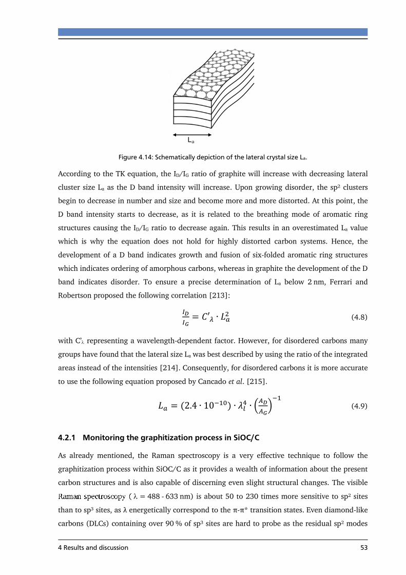
4 Results and discussion 53
Figure 4.14: Schematically depiction of the lateral crystal size La.
According to the TK equation, the ID/IG ratio of graphite will increase with decreasing lateral
cluster size La as the D band intensity will increase. Upon growing disorder, the sp² clusters
begin to decrease in number and size and become more and more distorted. At this point, the
D band intensity starts to decrease, as it is related to the breathing mode of aromatic ring
structures causing the ID/IG ratio to decrease again. This results in an overestimated La value
which is why the equation does not hold for highly distorted carbon systems. Hence, the
development of a D band indicates growth and fusion of six-folded aromatic ring structures
which indicates ordering of amorphous carbons, whereas in graphite the development of the D
band indicates disorder. To ensure a precise determination of La below 2 nm, Ferrari and
Robertson proposed the following correlation [213]:
𝐼𝐷
𝐼𝐺= 𝐶′𝜆 ∙ 𝐿𝑎
2 (4.8)
with C’ representing a wavelength-dependent factor. However, for disordered carbons many
groups have found that the lateral size La was best described by using the ratio of the integrated
areas instead of the intensities [214]. Consequently, for disordered carbons it is more accurate
to use the following equation proposed by Cancado et al. [215].
𝐿𝑎 = (2.4 ∙ 10−10) ∙ 𝜆𝑙4 ∙ (
𝐴𝐷
𝐴𝐺)−1
(4.9)
4.2.1 Monitoring the graphitization process in SiOC/C
As already mentioned, the Raman spectroscopy is a very effective technique to follow the
graphitization process within SiOC/C as it provides a wealth of information about the present
carbon structures and is also capable of discerning even slight structural changes. The visible
= 488 - 633 nm) is about 50 to 230 times more sensitive to sp² sites
than to sp³ sites, as λ energetically correspond to the π-π* transition states. Even diamond-like
carbons (DLCs) containing over 90 % of sp³ sites are hard to probe as the residual sp² modes

54 4 Results and discussion
superimpose the whole Raman spectrum. By using the UV Raman spectroscopy
( = 320 – 280 nm), this problem can be avoided. With its higher photon energy of 4.4 - 5.1 eV,
UV Raman spectroscopy excites both the π and the σ states which allows to probe sp³ sites
occurring at early stage of graphitization. However, the sensitivity for the sp² modes is still
stronger by a factor of 5 - 10 compared to the sp³ sites [216]. Nevertheless, the UV Raman
spectroscopy does provide an equal excitation of both graphitic and olefinic components, as it
excites not just the lower lying π states [217]. As all vibrations of the sp² carbons are induced
equally, a more detailed investigation of various sp² structures and even to some extent of sp³
structures are possible. Thus, the UV Raman spectroscopy is a valuable tool to follow the initial
graphitization steps during the synthesis of the SiOC/C ceramic.
In the following, the graphitization process of a carbon depleted C-1 and a carbon-rich C-11
sample are examined with UV Raman. In case of the C-1 sample, the low amount of carbon
allows to assess the initial carbon which segregates in the early beginning at temperatures
T < 1000 °C as the carbons precipitations are encapsulated and spatially separated by the
ceramic network. In contrast, the precipitations in the C-11 sample already show first signs of
graphitic order. Both UV Raman spectra are compared in Figure 4.15.
Figure 4.15: Comparison of the UV Raman spectra of C-1 and C-11 sample prepared at T = 1000 °C.
The C-1 sample does not exhibit any typical resonances of graphitic (1580 cm-1) or diamond-
like carbon (1333 cm-1). Therefore, the signals at wave numbers > 1000 cm-1 are considered to
belong to non-graphitic carbon. The most prominent feature at 1500 cm-1 can be attributed to
the E2g mode (G band) of amorphous carbon where conjugated sp² bonds (ring- and chain-like
structures) coexist with sp³ single bonds. According to the elemental analysis, the C-1 sample
contains significant amounts of hydrogen (≈ 24 mol.%), suggesting that amorphous

4 Results and discussion 55
hydrogenated carbon (a:C-H) is formed. The band at 1115 cm-1 indicates the presence of
polyacetylene (-CH=CH-)n with chain lengths in the order of n ≈ 10 [218]. Configurational and
conformational deformation leads to the strong broadening of the Raman signal. Small
polycyclic aromatic hydrocarbons (PAHs) are identified by the signal at 1360 cm-1 and the C-C
single bonds (sp³) by the signal at 980 cm-1. Finally, the broad resonances appearing at 345,
510 and 830 cm-1 correspond to the glassy SixOyCz network (Si-O, Si-O and Si-C). The Raman
spectrum of the C-11 sample, in contrast, is dominated by a strong G feature at 1580 cm-1 and
a weak D mode which can be attributed to nano-graphitc carbon. In between these two signals
lies the resonance of a-C:H. The signal of polyacetylene (-CH=CH-)n is also present, but its
intensity is much lower as their concentration has already declined at the expense of
nano-crystalline graphite. Interestingly, no Raman features of the SixOyCz matrix are found in
C-11 which is probably due to the much greater intensity of the present sp² features dominating
the Raman spectrum.
Figure 4.16: Comparison of the UV Raman spectra of C-1 and C-11 sample prepared at T = 1400 °C.
Raising the pyrolysis temperature up to T = 1400 °C results in a more ordered carbon, as shown
in Figure 4.16. In both spectra, the features below 1300 cm-1 have vanished leaving only the
typical sp² carbon signals i.e. D (≈ 1400 cm-1), a-C (≈ 1500 cm-1) and G (≈ 1600 cm-1) with
different relative intensities. In case of the C-1 sample, a weak G and D mode appeared at the
expense of the olefinic chains and PAHs, whereas a strong resonance of a-C remains. As
supported by elemental analysis, the change in the carbon microstructure results from the loss
of hydrogen at temperatures in the range of T = 1000 - 1250 °C: breaking up the C-H bonds
which promotes the formation of aromatic sp² bonded carbon. Nevertheless, the strong feature
of a-C still indicates an early stage of graphitization. The UV Raman spectrum of the C-11

56 4 Results and discussion
sample is comparable with the spectrum at T = 1100 °C with only slight changes such as the
vanished signal of the olefinic chains and the grown intensity of the D mode. By comparing the
two Raman spectra, graphitic domains appears to form more easily in carbon-rich samples and
the transformation to nano-crystalline graphite can be regarded as finished when the a-C signal
disappears.
Figure 4.17: UV Raman spectra of sample C-11 prepared at 1600 °C. The inset shows the second order UV
Raman spectrum.
Figure 4.17 presents the UV Raman spectra of C-11 pyrolyzed at T = 1600 °C. The band
attributed to a-C has faded and the characteristic UV Raman bands of graphitic carbon are
present: the G band at 1580 cm-1 and the complex signal at ≈ 3000 cm-1 due to the double
resonance scattering. The inset in Figure 4.17 displays the deconvolution of the latter signal.
The peak positions of the fitted lines are in excellent agreement with the literature UV Raman
data for graphite with the only remarkable difference being the broadening of the Raman lines
(by a factor of ≈ 5) which very likely arises from the higher distortion of graphite within the
glassy matrix. Note that the obtained data rule out graphene as carbon component, as the UV
Raman spectrum of graphene shows a less marked signal structure, i.e. fewer peaks are
observed in the range of 2600 to 3400 cm-1. The weak but still visible D peak and the change in
the full width half maximum (FWHM) of the G band also hint at non-ideal graphite. The FWHM
exceeds the value of highly-ordered graphite by far (FWHMHOPG = 10 cm-1) and decreases only
slightly from 51 cm-1 (T = 1400 °C) to 47 cm-1 (T = 1600 °C). This also applies for the G band
of the C-1 sample with a FWHM of 45 cm-1 at T = 1600 °C. Consequently, the transformation of
amorphous carbon to nano-crystalline carbon at T > 1400 °C is seen in the Raman spectrum of
C-1 and C-11 by the decrease of the a-C signal and the appearance and increase of the G band.

4 Results and discussion 57
Upon further thermal annealing to T = 1600 °C, the nano-crystalline carbon phase gradually
transforms into disordered graphite-like carbon. In agreement with previous TEM studies,[183]
the obtained results suggest the presence of turbostratic carbon within the silica matrix and do
not support the model description of carbon as a network of single layer graphene bonded to
silica SiOmC4-m tetrahedra [30].
4.2.2 Characterization of the segregated carbon phase by Vis Raman
Figure 4.18 displays the visible Raman spectrum ( = 514 nm) of a C-11 sample heat treated
at different temperatures. It can be easily noted, that the evolution of the spectrum reflects the
advancing graphitization within the sample. For the least ordered sample at T = 1000 °C, two
broad signals representing the D and G band, along with a very broad signal at 1120 cm-1
(T band) are obtained. No spectral changes are observed until the thermal treatment is
increased up to T = 1400 °C. Hereby, the T band, induced by residual sp³ carbon, vanishes and
the FWHM of the D band significantly narrows along with an increasing intensity. The width
and intensity of the G band stays constant but a small shoulder around 1620 cm-1 starts to
develop. The occurred D’ band supports the evolution of small nano-graphitic clusters which is
also substantiated furthermore by the development of two signals (2D and D+G) in the
second-order spectrum.
Figure 4.18: Evolution of the Raman spectrum obtained at = 514 nm for C-11 samples heat-treated at
different temperatures (1000 < T < 1800 °C).
With increasing crystalline order, the D band continuous to narrow and the D’ band becomes
more and more pronounced together with a displacement of the G band towards lower
wavelengths. Although the advancing graphitization does not increase the intensity of the G

58 4 Results and discussion
band, the two signals in the second-order spectrum clearly improve their intensity. In the final
spectrum at T = 1800 °C the intensity of the G band is notably increased and the wavelength is
downshifted by 30 cm-1, with the D’ band remaining as a small shoulder. In addition, the second-
order spectrum markedly differs from the previous ones as the band at 2700 cm-1 has apparently
grown in intensity and is displaced by 15 cm-1 to lower wavelength. According to Pimenta et al.,
the shape and shift of this band resembles turbostratic stacking of several graphene sheets along
the c-axis as the width of the feature (w = 77 cm-1) is notably larger than that of monolayer
graphene (w = 24 cm-1) [219]. The progressive changes in the Raman spectrum represent the
current intermediate stages during the transition from amorphous to nano-crystalline and
eventually to turbostratic micro-crystalline carbon. The spectral parameters for the
characteristic first-order Raman spectrum are given in Table 4.3.
Table 4.3: Summary of the features present in the first-order Raman spectrum of C-11.
C-11 T
(cm-1)
AT
(cm-1)
D
(cm-1)
AD
(cm-1)
G
(cm-1)
AG
(cm-1)
D'
(cm-1)
AD'
(cm-1) AD/AG
1000 °C 1204 10.7 1348.9 117.2 1593.1 51.2 - - 2.3
1200 °C 1193 12.1 1348.6 107.6 1594.7 42.1 - - 2.5
1400 °C - - 1349.2 119.8 1597.2 54.6 1623.7 2.1 2.2
1500 °C - - 1354.8 93.7 1597.3 40.8 1624.3 4.3 2.2
1600 °C - - 1350.6 77.1 1581.6 48.3 1625.0 4.6 1.59
1800 °C - - 1342.9 48.6 1563.4 56.5 1611.8 1.8 0.86
The elimination of defects and the growth in crystalline size is also reflected by the change of
the FWHM of the D and G band depicted in Figure 4.19. Both features possess a broad signal
up to T = 1200 °C which is mostly caused by different carbon species within the amorphous
carbon phase, such as PAHs, polymeric chains, sp³ carbon and defective nano-graphite.
Especially, the D band reacts sensitive to this kind of non-graphitic structures as they enable its
Raman vibration mode. With increasing thermal treatment beyond T > 1350 °C, the SiOC
matrix starts to separate into SiO2 and SiC. The separation process promotes clustering of the
spatially separated carbon domains which themselves continues to accumulate at the expense
of residual sp³ carbon and olefinic chains. However, the resulting carbon phase is still of highly
defective nature and far from being well-ordered.

4 Results and discussion 59
Figure 4.19: Progressive change of the FWHM of the D and G band upon thermal treatment.
The existence and the relative small drop of the G band compared to the degression of the D
band supports the assumption that, when the amount of carbon is sufficient enough, the
nano-graphitic core structures are almost present at T = 1000 °C [220]. Upon further heating,
the internal lattice defects of the graphitic crystals slowly starts to vanish resulting in a decline
of the G linewidth. The accompanied decline of the D width mirror the rearrangement of the
surrounding and the eradication of intrinsic defects. At T = 1800 °C the width of the D and G
band lies around w = 50 cm-1 which corresponds to the width of microcrystalline graphite
(wD = 66.6; wG = 59.9) and glassy carbon (wD = 52.7; wG = 56.1) whereas the segregated
carbon at T = 1000°C resembles coke (wD = 149.1, wG = 79) [221]. Nevertheless, even after
the highest temperature treatment a high amount of intrinsic defects remains represented by
the intense D band.
Figure 4.20 shows the lateral crystal size La and its progress with increasing thermal treatment
calculated according to Equation 4.9. From the graph it can be derived that the lateral crystal
size is not affected up to T = 1500 °C and only slightly varies around a value of La = 7.5 nm.
This is supported by the work of Takai et al. who obtained similar values (La = 5 - 7 nm) for an
amorphous carbon film heat treated in the temperature range up to T = 1500 °C. At higher
temperatures, the crystalline lattice starts to grow as the intrinsic lattice defects are removed.
The onset of graphitization is emphasized by the increase in intensity of the G band and the
clear development of D’ at T = 1600 °C, see Figure 4.18.

60 4 Results and discussion
Figure 4.20: Dependency between the lateral crystal size La and the thermal treatment. The open data
points in the inset represent the work of Ref. [215].
Similar findings but at a much higher temperature readings were published by Cancado et al.
who investigated the graphitization behavior of diamond-like carbon thin films [215]. Their
results are given by the empty dots in the inset of Figure 4.20. According to their XRD
measurements a La value of La = 20 nm is obtained after a thermal treatment of T = 1800 °C
which is in perfect agreement with the La value found in the SiOC/C sample. Although higher
thermal treatment promotes graphitization, it also supports the degradation of the SiOC
network due to the carbothermal reaction (Equation 2.3). Therefore, the samples are prepared
at T = 1600 °C resulting in smaller graphitic crystals with a size of La = 10 ± 2 nm.
To verify if the amount of segregated carbon also affects the lateral size of the graphitic
crystallites, several SiOC/C samples with varying amounts of carbon were investigated. The
results are depicted in Figure 4.21 and reveal a constant lateral crystal size of La = 9 ± 1 nm
for samples with a carbon content above C > 10 vol.%. In case of lower carbon contents,
(C < 10 vol.%) smaller crystallites in the range of La = 6 ± 2 nm are obtained. The observed
trend supports the earlier postulated assumption that the formation of nano-crystalline graphite
is promoted in carbon-rich samples.

4 Results and discussion 61
Figure 4.21: Plot of the lateral crystal size La as a function of the amount of carbon.
The evolution of disorder within the graphitic crystals can also be characterized as a function
of the average distance between defects LD and the ratio AD/AG. The average distance is
calculated according to the following equation 4.10 [222]. Figure 4.22 depicts the obtained LD
values of C-11 together with an Ar+ ion bombarded graphene layer as reference.
𝐿𝐷2 = 1.8 ∙ 10−9 ∙ 𝜆𝐿
4 ∙ (𝐴𝐷
𝐴𝐺)−1
(4.10)
As can been seen in Figure 4.22, the AD/AG ratio of the graphene layer increases linearly up to
a maximum value of AD/AG ≈ 3.2. The rising AD/AG ratio resembles ordering of the defective
crystallites which are initially too small to contribute to the Raman spectrum. As the Ar+ ion
dose is constantly reduced, less defective crystallites are produced, causing the AD/AG ratio to
increase to its maximum. The subsequent decrease of the AD/AG ratio, is caused by further
ordering of the crystallites and the accompanied decreasing D band. A similar behavior was
observed by Ferrari et al. who divided the course of the ratio AD/AG according to the crystalline
size La into stage 1: high defect concentration ID/IG=1/La2 and stage 2: low defect
concentration, ID/IG=1/La. They proposed that the TK Equation 5.1 is only valid in stage 2 and
breaks down below La < 2 nm. The transition is usually observed in the range of AD/AG ≈ 3 at
λ = 514 nm which corresponds to the course in Figure 4.22. With regards to C-11 the calculated
values follow the decline of the AD/AG ratio with increasing crystalline order as the thermal
treatment is raised. At T = 1000 °C a LD value of 6 nm is obtained which means that within the
average lateral size of the crystallite (La 1000 °C = 7.5 nm) at least one defect is present. By
increasing the temperature up to T = 1400 °C, LD expands giving values in the range of
LD = 8 – 10 nm. This results in the development of the D’ band as it resembles nano-graphitic

62 4 Results and discussion
structures. Upon higher heat treatment, the intrinsic defects are further reduced giving rise to
higher LD and La values.
Figure 4.22: Evolution of the average distance between defects LD within the carbon of SiOC/C
synthesized at different temperatures. The empty dots represent Ar+ ion bombarded graphene [223].
Additional information about the nature of the present defects can be derived from the disorder-
activated features in the Raman spectrum. In general, one refers to defects in graphitic materials
as anything that breaks the symmetry of the honeycomb lattice causing the D band to appear.
Different kind of defects can be defined such as edges, grain boundaries, vacancies, implanted
atoms and different carbon hybridization. A systematic study to investigate the influence of the
respective defects in graphitic material was performed by Eckmann et al., see Figure 4.23 [224].
They plotted the intensity ration ID/IG versus ID’/IG following the disorder trajectory. Figure 4.23
reveals that for each individual type of defect a specific slope is obtained. According to their
work, sp³ hybridized graphene exhibits a slope of ID/ID’ ≈ 13, vacancies within defective
graphene revealed a slope of ID/ID’ ≈ 7 and the smallest slope with ID/ID’ ≈ 3.5 is obtained for
graphite with different grain sizes. As the slope is not dependent on the defect concentration,
it can be used to determine the dominant nature of defects. Note that for carbon-rich samples
(C > 17 vol.%) the D’ peak starts to merge with the G peak making it is difficult to separate the
individual contributions of the G peak and D’ peak. The linear fit of the obtained data reveals a
slope of ID/ID’ ≈ 6.5 which implies that the dominating nature of defects, for SiOC/C pyrolyzed
at T = 1600 °C, are vacancies and interstitial defects within the nano-crystalline carbon lattice
[225].

4 Results and discussion 63
Figure 4.23: ID/IG versus ratio ID’/IG. Data from literature is represented by open symbols [224].
It is not surprising that point-defects are found to be the dominant species as the UV Raman
measurements have already proven that neither sp³ defects nor graphene-like boundaries are
present in samples prepared at T = 1600 °C. Therefore, one can state that, the nature of defects
in SiOC/C is not controlled by the amount of carbon, but rather thermodynamically by the
applied temperature during the synthesis.
4.2.3 Summary
Two distinct well-defined types of carbon are generally assigned according to their
graphitization behavior: graphitizing and non-graphitizing carbons [77]. In non-graphitizing
carbons, no trace of developed graphitic structure can be detected even after heating to
T = 3000 °C. For graphitizing carbons, on the contrary, graphitization sets in at about
T ≈ 1700 °C and rapidly increases with increasing temperature. According to the Raman results
presented in this chapter, the segregated carbon in SiOC/C starts to graphitize around
T = 1600 °C and therefore can be assigned to the class of graphitizing carbons. In general, the
initial carbon segregating at T ≤ 1000 °C is being best described as an amorphous mixture of
chains, PAHs, nano-graphitic clusters and residual sp³ carbon as supported by the UV Raman
data. With increasing thermal treatment and the accompanied phase separation of the
amorphous SiOC matrix, the spatial separated carbon structures continue to aggregate at the
expense of the residual amorphous carbon. Figure 4.24 schematically depicts a cutout of a
nano-crystalline graphite at low temperature/high disorder. It consists of several carbon layers
with a lateral crystal size of La ≈ 10 nm. The layers are oriented in a turbostratic manner with a
locally preferred parallel orientation. Tilt and twist boundaries/defects exists within each layer

64 4 Results and discussion
forming wrinkled graphene-like sheets. These defects are assumed to be responsible for the
strong D feature present in the Vis Raman spectra.
Figure 4.24: Schematic depiction of a nano-crystalline cluster taken from Ref. [226].
The defects are spatially separated by an average distance of LD = 7 nm (at T = 1600 °C). The
lateral crystal size of the carbon layer remains almost constant up to T = 1600 °C. Upon further
thermal treatment (T = 1800 °C) La increases strongly and reaches values similar to those of
Cancardo et al. (La = 20 nm) who investigated the graphitization of DLC-films [215]. Even at
the highest synthesis temperature (T = 1800 °C) a strong D feature remains in the Raman
spectra indicating that the carbon phase in SiOC/C is still highly defective as most carbons need
temperatures in the range of 2000 - 2500 °C to delete the defects. Therefore, the segregated
carbon phase in SiOC/C can be best described as an intermediate stage between glassy and
graphitic carbon.
4.3 Electrical properties of SiOC/C
This chapter focuses on the electrical properties of SiOC/C. To gain further insight, Hall
measurements and temperature-dependent impedance spectroscopy were conducted. The dc
conductivity values were derived through extrapolation of the lowest frequency ( = 0.01 Hz)
to the x-axis intersection. A semicircle, which decreases in size with increasing temperature, is
obtained for all SiOC/C samples synthesized at temperatures below T < 1600 °C, regardless of
the amount of carbon. In contrast, samples synthesized at T = 1600 °C showed carbon
dependent impedance spectra with either ohmic resistance, obtained for samples with a high
carbon content (C > 10 vol.%), or a single semicircle for samples with a lower carbon content.
As main result of the impedance measurements no sign of second contribution to the
conductivity (contact or matrix dependent resistance) is observed in the most extensively
investigated samples prepared at T = 1600 °C. Since the bulk resistance obtained from the
impedance spectra equals the dc resistance only dc data are reported in the following.

4 Results and discussion 65
4.3.1 Resistance change with graphitization
PDCs develop a (segregated) carbon phase with pyrolysis which exerts a major influence on the
electrical properties [51, 165, 191, 227]. As the concentration and hybridization of carbon in
SiOC/C is strongly influenced by the initial polymer composition as well as the pyrolysis
condition (temperature, atmosphere and holding time), the resulting PDC ceramic can be
progressively changed from an insulator to a semiconductor and semimetal. The electrical
properties therefore represent a sensitive measure of the state of carbon during preparation and
provide valuable information on the graphitization process.
Figure 4.25 depicts the room temperature conductivity of sample C-11 and C-17 synthesized at
T = 1200 – 1800 °C. Literature data of glassy carbon are added for comparison [55]. Both
samples exhibit semiconductive behavior with values between σ = 10-4 - 10-2 (Ω∙cm)-1 at
T > 1400 °C. The increase in σ observed for C-11 and C-17 around T = 1300 - 1400 °C is due
to the change in porosity during densification of the sample. Therefore, only σ values obtained
at T > 1400 °C represent the bulk conductivities of C-11 and C-17. The higher conductivity of
C-17 is caused by the higher amount of segregated carbon.
Figure 4.25: Effect of heat-treatment temperature on the RT-conductivity of C-11, C-17. Literature data is
taken from Ref. [53, 228].
The activation energies Ea for the electrical transport in C-11 and C-17
(2.7 ± 0.4 eV; 2.3 ± 0.4 eV), representing the energy for graphitization, are consistent with
literature data of other PDC systems and are in accordance with the graphitization energy found
in amorphous carbon (3.3 eV, [229]).
4.3.2 Percolation in SiOC/C
The carbon distribution in low conducting and highly conducting samples is schematically
depicted in Figure 4.26. Assuming an ideal two components system (non-interacting phases)

66 4 Results and discussion
the conductivity will be given by the volume fractions i and the partial conductivities σi of the
two components: σtotal = σglass∙glass + σcarbon∙carbon. In both cases the overall conductivity is
determined by the carbon phase since σcarbon is by orders higher than σglass.
Figure 4.26: Schematic depiction of the carbon distribution within SiOC/C.
Increasing the carbon volume fraction C may lead to a percolation type conductivity. Below
the critical volume fraction cri. no continuous path for the charge transport exists whereas
above cri. the charge carriers can be transported efficiently without restriction along the carbon
path. Figure 4.27 shows the (logarithmic) room-temperature dc conductivity of the SiOC/C
samples with carbon concentrations C = 1 – 43 vol.% synthesized at 1100 < T < 1600 °C.
Based on the Raman data (Chapter 4.2) carbon is mainly sp² hybridized. Therefore, the carbon
concentration is expressed as the sp² volume fraction. The critical concentration (percolation
threshold) varies from about 20 – 6 vol.% sp² carbon depending on the synthesis temperature.
At this concentration the conductivity changes by order of magnitude due to the transition from
insulating to semiconducting / almost semimetallic SiOC/C. It is tempting to attribute the
decrease of the percolation threshold to an increase in the aspect ratio of the segregated carbon
phase, as the threshold depends on the shape of the conductive filler in many composite
materials [230-232]. However, no reliable information on the aspect ratio can easily be
obtained for SiOC/C, due to the random 3D carbon morphology and the lack of suitable
characterization methods. Hence, Cordelair et al. computed the insulator-conductor transition
in SiOC/C showing that the threshold decreased from 20 to 5 vol.% when the shape of the
conductive filler was changed from spherical to rod-like carbon precipitations, see Figure 2.4
[49].

4 Results and discussion 67
Figure 4.27: The electrical conductivity of SiOC/C as a function of the sp² carbon for three different
temperature series. Literature values are added for the sake of comparison.
According to the Raman data carbon mainly exists as a sp² network. Even for the C-1 sample
the network carbon dominates over the smaller aromatic structures (PAHs, polyacetylene), see
Figure 4.15, raising doubts about the importance of well-defined geometrical conductive fillers
used in the proposed model. The observed shift in cri. may also be caused by changes in the
carbon network itself, e.g. the loss of defects and the resulting better alignment of carbon sheets
allowing enhanced electrical transport in conjugated bonds. A further sign that geometrical
aspects are less important for the percolation in SiOC/C is given by the critical exponent t
derived from the ln (σ/σ0) versus ln (-cri.) plot (Figure 4.28). The value for the critical
exponent derived from Equation 2.4
𝜎𝐶 = 𝜎0 ∙ (𝐶 −
𝑐𝑟𝑖.)𝑡 (2.4)
differs strongly from the (solely geometrically defined) universal value of 2 for three-
dimensional systems.
For SiOC/C prepared at T = 1600 °C with a critical volume concentration of 6 vol.% a value of
t = 4.3 is obtained which is very similar to that of RuO2/silica (t = 3.8), a well-known fine
dispersed composite. Non-universal behavior is frequently observed in dispersed composites,
whereas universal behavior is seen more often in clustered samples [46]. The non-universal
behavior may result from tunneling/hopping processes between two adjacent conductive
particles [233], e. g., taking quantum mechanics into account the critical exponent becomes
dependent on the mean tunneling distance and in principle does not obey any upper limit.

68 4 Results and discussion
Figure 4.28: Electrical conductivity as a function of sp² carbon concentration. The solid line represents the
fit from Equation 2.4. The upper dashed line represents the universial behavior with a slope of t = 2.
4.3.3 Conduction mechanism in SiOC/C
A broad range of different carbon microstructures can be present in SiOC/C ceramics depending
on the synthesis conditions. Consequently, it covers a wide range of electronic properties. At
one extreme, the electronic conduction approximates that of graphite, whereas on the other
extreme, the present carbons can be considered as an inhomogeneous mixture of partially
polymeric molecules encapsulated by an insulating silica-near matrix. In between these two
extremes, disorder of various kinds modifies the electronic structure in several ways.
The most comprehensive description of the electrical properties of amorphous materials like
SiOC/C was given by Mott and Elliot (see chapter 2.2.2) [86, 234]. They describe the
conduction in strongly disordered systems with localized states at the tails of the valence and
conduction bands as well as midgap states at the Fermi level. Two hopping mechanisms are
discussed: the nearest neighbor hopping (NNH) mechanism within the tail states and the
variable range hopping mechanism (VRH) near the Fermi level. The latter hopping mechanism
is distinguishable from the other conduction mechanisms by its different temperature
dependence: log σ ≈ T-1/4 at low temperatures (typically 4 < T < 300 K). With increasing
temperature the hopping regime changes into the Arrhenius type conduction mechanism
(log σ ≈ T-1). Therefore, the thermal dependence of the conductivity is an effective and
informative electrical property providing information about the present conduction mechanism.
In case of electrons or holes as majority carriers hopping in localized states can occur as depicted
in Figure 4.29a) and Figure 4.29b).

4 Results and discussion 69
Figure 4.29: Schematically depiction of the electronic transport of a) electrons and b) holes within the
localized states.
Only few information about the conduction mechanism in PDCs is available in literature.
Haluschka and Engel report on SiCN/C (C = 5 vol.%) and SiOC/C (C = 12 vol.%) prepared
at T = 1500 °C and T = 1300 °C [51, 235]. Both authors interpreted their data within the VRH
model. A T-1/4 dependency was found up to T = 800 °C. Haluschka et al. could further prove,
that the conduction occurs by phonon-assisted hopping near the Fermi-energy and not near the
mobility edges. Engel estimated the density of states near the Fermi energy to be between
N = 1017 - 1019 eV-1cm³ by assuming a localization length of α-1 = 10 Å common for amorphous
semiconductors. Ma et al. investigated SiCN/C (C = 22 vol.%) claiming nearest neighbor
hopping also called band tail hopping (BTH) as transport mechanism on account of the
correlation between the parameters σ0 and T0 in the general equation for transport in localized
states [228]:
𝜎 = 𝜎0 ∙ [− (𝑇0
𝑇)1/𝛽
] (4.11)
Figure 4.30 shows the Arrhenius plot of C-11 prepared at temperatures between
T = 1000 - 1600 °C. Above T > 1400 °C a linear dependency of σ with T-1 is evident indicating
activated transport with Ea = 0.23 eV and Ea = 0.04 eV whereas below that temperature a non-
linear behavior is observed. Plotting the low temperature data against T-1/β (β = 3, 4) yields no
clear evidence of non-Arrhenius behavior. Assuming activated transport for the T = 1000 °C
and T = 1200 °C samples two different activation energies, see Figure 4.30, may therefore
occur, due to two different contributions to the conductivity. However, one can not rule out
that both VRH and thermally activated transport exist in this temperature range. Further
measurements are needed for clearance. The decreasing activation energies with increasing
synthesis temperature indicate the continuous reduction of the band gap, since for the highest
synthesis temperature (T = 1600 °C) the activation energy is comparable to that of glassy
carbon (Ea = 0.03 eV [59]).

70 4 Results and discussion
Figure 4.30: Electrical conductivity of C-11 as a function of temperature.
It appears that the conduction in carbon-rich SiOC/C changes with synthesis temperature from
VRH (or BTH) to activated Arrhenius-type transport and semimetallic transport in -conjugated
extended states.
Figure 4.31 plots the activation energy Ea as a function of the segregated carbon for samples
prepared at T = 1600 °C. The activation energies were derived from the dc conductivity (σ0.01Hz)
in the temperature range of 200 ≤ T ≤ 800 °C. Three different electrical transport regimes can
be distinguished as the activation energy decreases from Ea = 1 to 0.3 eV and finally to
0.028 eV.
Figure 4.31: Ea of the different conduction mechanism in SiOC/C derived from dc conductivity in the temperature regime of 200 ≤ T ≤ 800 °C as a function of the sp² carbon.

4 Results and discussion 71
In the first regime I, conduction occurs within the amorphous silica network as the amount of
sp² carbon is very low (C < 1 vol.%) and spaciously separated. According to Hapert a high
concentration of silicon dangling bonds are present within a-SiOx, showing a VRH transport
within localized states [229]. A VRH conduction mechanism is also likely for carbon-depleted
SiOC, due to the defective microstructure of the SiOC matrix.
In the second (semiconducting) regime II (C = 2 - 6 vol.%) the graphitic precipitations are still
separated by the SiOC matrix but the resulting potential barrier for the transport is lowered
(Ea ≈ 0.3 eV). The low activation energy arises from additional carbon defects states within the
band gap presumably overlapping with the silicon dangling bonds states. A very similar
activation energy (Ea = 0.3 eV) has been found by Dasgupta et al. who investigated hopping
between graphitic islands separated by a lower conducting sp³ layer [81].
In the last regime III, the carbon concentration is above the percolation threshold for samples
prepared at T = 1600 °C. Thus, the electrical transport is dominated by the continuous, three
dimensional carbon sp² network yielding activation energies in the range of
Ea = 0.035 - 0.02 eV, which perfectly resemble the conduction energies found in glassy carbon
[55]. The transition from semiconducting to semimetallic conduction is accompanied by the
reduction of the gap between carbon and * band states. Carbon essentially controls the
density of states, whereas the SiOC states are of minor importance within the third regime.
Hence, the same transport mechanism prevails for all samples above the percolation threshold
and can be illustrated by the following scheme (Figure 4.32).
Figure 4.32: Schematically depiction of the shallow traps within the conjugated -system.
Herein l1 corresponds to transport in conjugated -bonds within the carbon network, l2
represents a shallow carbon defect. This (simplified) model description is supported by the
observed constant carrier mobilities form the Hall measurements (Figure 4.33) and the
activation energies of Ea ≪ 0.1 eV from the conductivity studies within 8 < C < 46 vol.%.
The electrical behavior of SiOC/C can be correlated with the Raman data obtained in
chapter 4.2.2. The activation energy Ea changes inversely with the lateral crystal size La
assuming that the width of the band gap depends on the concentration of carbon precipitations
(Equation 4.12 and Equation 4.13):

72 4 Results and discussion
𝐸𝑎 =2.1
𝐿𝑎 for carbon based semiconductors [89] and (4.12)
𝐸𝑎 =7.7
𝐿𝑎 for graphitic-like materials [236]. (4.13)
An activation energy of Ea = 0.28 eV is calculated from Equation 4.12 for the semiconducting
samples with an average lateral crystal size of La = 7.5 nm, which is in excellent agreement with
the Ea values from conductivity (Figure 4.31). For graphitic-like materials with La = 9 nm an
activation energy of Ea = 0.085 eV is obtained from Equation 4.13 which is of the same order
as Ea determined by the conductivity (Ea = 0.035 - 0.02 eV).
4.3.4 Hall measurements of SiOC/C
Information about the density and mobility of the dominant carrier type is generally provided
by measurements of the Hall Effect. Figure 4.33 plots the carrier density (N) and mobility (µ)
as a function of the carbon content for SiOC/C samples prepared at T = 1600 °C. Literature
values of an SiOC/C synthesized at T = 1550 °C are displayed for comparison [237]. Data for
the density or mobility can be also obtained from conductivity measurements if the electrical
transport solely depends on one charge carrier type (electrons or holes):
𝜎 = 𝑒 ∙ 𝑁 ∙ 𝜇 (4.14)
The carrier densities derived from dc measurements (Figure 4.27) are shown in Figure 4.33
(green circles) as a function of the carbon concentration using the experimentally determined
mobility of µ = 3 cm2/Vs which is similar to that of turbostratic carbon (µ = 3.1 – 6.3 cm²/Vs
[54, 88]). The dc- and Hall-densities perfectly agree above a carbon concentration of ≈ 8 vol.%
and are in accordance with values found in glassy carbon [76, 238]. Below this concentration
the carrier densities from dc- and Hall-conductivity measurements differ substantially and
agreement can only be obtained if a mobility of localized carriers, typically µ = 10-4 cm²/Vs
[234], is assumed. Unfortunately, Hall measurements for samples with rather low conductivity
or electrical non-uniformity are experimentally challenging and the few data obtained for
C < 8 vol.% allow no clear decision.
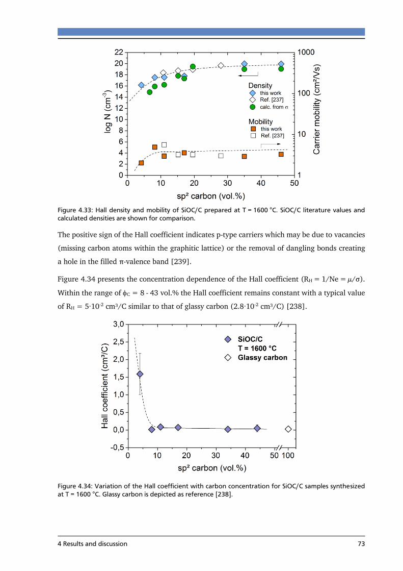
4 Results and discussion 73
Figure 4.33: Hall density and mobility of SiOC/C prepared at T = 1600 °C. SiOC/C literature values and
calculated densities are shown for comparison.
The positive sign of the Hall coefficient indicates p-type carriers which may be due to vacancies
(missing carbon atoms within the graphitic lattice) or the removal of dangling bonds creating
a hole in the filled π-valence band [239].
Figure 4.34 presents the concentration dependence of the Hall coefficient (RH = 1/Ne = µ/σ).
Within the range of C = 8 - 43 vol.% the Hall coefficient remains constant with a typical value
of RH = 5∙10-2 cm³/C similar to that of glassy carbon (2.8∙10-2 cm³/C) [238].
Figure 4.34: Variation of the Hall coefficient with carbon concentration for SiOC/C samples synthesized
at T = 1600 °C. Glassy carbon is depicted as reference [238].

74 4 Results and discussion
Positive Hall coefficients of the same order have been also reported for nano-crystalline graphite
(La < 30 nm [240, 241]). According to Ref. [242] the Hall coefficient increases with increasing
disorder and only turns negative in better crystallized graphite (La ≫ 100 nm).
At lower carbon concentrations (C < 8 vol.%) the Hall coefficient increases by two orders of
magnitude indicating less ordered crystalline carbon in SiOC/C. This result is supported by the
Raman data showing a change of the lateral crystal size La and average defect distance LD in the
same concentration region (Figure 4.21 + Figure 4.22). Furthermore, the activation energy for
the conductivity (Figure 4.31) increases to ≈ 0.3 eV for C < 8 vol.%.
In summary, the results obtained from the different experiments suggest a change from
band-like transport to conduction in localized states which very likely arise from electron/hole
confinement when the localization length approaches a lateral crystal size of about La = 10 nm.
4.3.5 Summary
The electrical properties of SiOC/C vary strongly with the morphology of carbon and the SiOC
matrix and indicate a change from conduction in localized states to band-like transport with
increasing carbon content. Insulating (σ < 10-10 (Ω∙cm)-1), semiconducting (σ < 10-4 (Ω∙cm)-1)
or semimetallic (σ < 102 (Ω∙cm)-1) transport can be distinguished depending on the
concentration and the degree of order within segregated carbon. The transition to highly
conducting SiOC/C - at the percolation threshold - depends on the volume concentration of
carbon and the synthesis temperature which defines the stage of graphitization or degree of
ordering. In case of samples synthesized at T = 1600 °C the continuous nano-crystalline
graphitic network is formed at cri. = 6 vol.% carbon. The percolation threshold shifts to about
20 vol.% for less ordered samples synthesized at 1100 °C. The conductivity shows a power–law
dependence with a critical exponent of about 4 which differs markedly from the (solely
geometric defined) universal value t = 2 for 3D systems indicating that chemical or physical
effects dominate when carbon remains dispersed in the glassy matrix.
Concerning the charge transport mechanism in SiOC/C different conduction regimes can be
distinguished for samples prepared at T = 1600 °C. Above the percolation threshold σ is very
weakly activated (Ea < 0.03 eV) and the transport is realized within conjugated -bonds.
Tunneling or hopping of charge carriers between spatially separated graphitic islands appears
to be responsible for the electrical conductivity near the percolation threshold. At very low
carbon concentrations (C < 1 vol.%), the glassy matrix defines the electrical transport: the
activation energy of ≈ 1 eV indicates transport within localized states, presumably silicon
dangling bonds.

4 Results and discussion 75
The charge carrier density of SiOC/C (T = 1600 °C) determined by Hall measurements varies
with the carbon content from about 1014 to 1019 cm-³ within 4 < C < 46 vol.% carbon. The Hall
mobility stays constant above the percolation threshold (C ≈ 6 vol.%) and has a value of about
3 cm²/Vs, very similar to that of turbostratic carbon. Below cri. the mobility starts to decrease
indicating charge carrier localization. The charge carrier densities obtained from the Hall effect
(NH) and the calculated values from the dc conductivity (Ndc) agree within the experimental
error providing evidence that one type of carrier dominates. The positive sign of the Hall
coefficient suggests p-type carriers.
4.4 The piezoresistive effect in SiOC/C
Very little is known about the piezoresistive effect in amorphous semiconductors, due to their
highly distorted structure and their complex conduction mechanisms. Even in crystalline
semiconductors the piezoresistivity of n-type semiconductors, such as Si, Ge, has not been
successfully described until the year 1954, while the effect of their p-type analogues still
remains unsolved due to the complexity of the valence band structure [243, 244]. It would be
presumptuous to claim that this chapter is able to clarify the origin of the piezoresistive behavior
of nano-heterogeneous SiOC/C. Instead, it rather tries to convey a phenomenological
description by investigating its dependency on carbon concentration and temperature.
A short overview of the experimental setup and the determination of the gauge factor (GF) by
two different methods is provided in the following.
Two experimental setups, schematically depicted in Figure 4.35, have been developed in
cooperation with the Electromechanical Department (EMK) at the TU Darmstadt in order to
assess the piezoresistive behavior of SiOC/C. In the first setup, depicted in Figure 4.35a), the
sample is clamped into the beam and strain is applied by a weight. FEM simulations, performed
at the Institut of Electromecanical Department in the working group of Prof. Roland
Werthschützky, show the distribution of the tensile (red) and compression forces (blue) and
reveals that only compressive stress has to be considered in the sample region, see Figure 4.36.
Figure 4.35: Schematic depiction of the developed setups, a) bending beam and b) measurement
chamber.
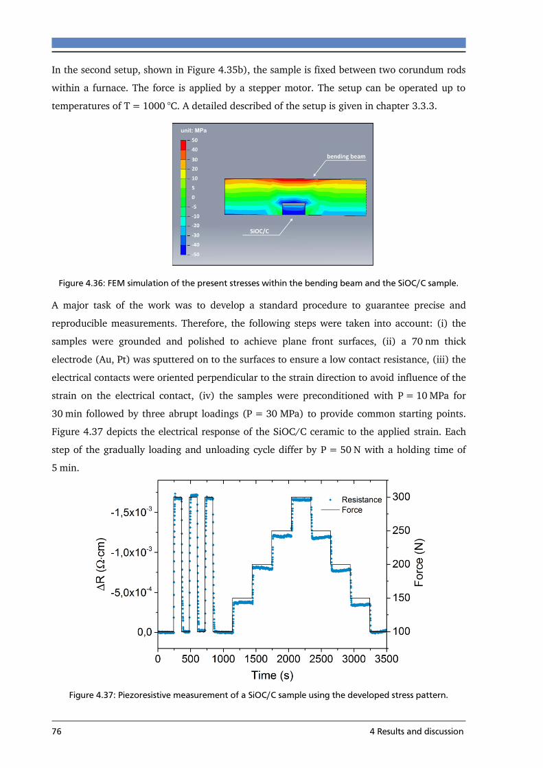
76 4 Results and discussion
In the second setup, shown in Figure 4.35b), the sample is fixed between two corundum rods
within a furnace. The force is applied by a stepper motor. The setup can be operated up to
temperatures of T = 1000 °C. A detailed described of the setup is given in chapter 3.3.3.
Figure 4.36: FEM simulation of the present stresses within the bending beam and the SiOC/C sample.
A major task of the work was to develop a standard procedure to guarantee precise and
reproducible measurements. Therefore, the following steps were taken into account: (i) the
samples were grounded and polished to achieve plane front surfaces, (ii) a 70 nm thick
electrode (Au, Pt) was sputtered on to the surfaces to ensure a low contact resistance, (iii) the
electrical contacts were oriented perpendicular to the strain direction to avoid influence of the
strain on the electrical contact, (iv) the samples were preconditioned with P = 10 MPa for
30 min followed by three abrupt loadings (P = 30 MPa) to provide common starting points.
Figure 4.37 depicts the electrical response of the SiOC/C ceramic to the applied strain. Each
step of the gradually loading and unloading cycle differ by P = 50 N with a holding time of
5 min.
Figure 4.37: Piezoresistive measurement of a SiOC/C sample using the developed stress pattern.

4 Results and discussion 77
The main parameter for strain sensing is expressed by the gauge factor (GF). In order to
determine GF, the strain ε has to be calculated first:
𝜀 = 𝐹
𝐸∙𝐴 (4.15)
with F being the applied force, E the Young’s modulus of the material (ESiOC/C = 100 MPa) and
A the contact area of the sample. GF is then defined as the ratio of the fractional change of the
electrical resistance to the applied strain,
𝐺𝐹 =∆𝑅
𝑅0∙1
𝜀 (2.12)
with R0 the electrical resistance at steady-state and ΔR the resistance change caused by the
strain. Figure 4.38 presents a typical piezoresistve measurement at RT on a C-17 sample
synthetized by T = 1600 °C.
Figure 4.38: Determination of the GF value by plotting the relative resistance change against the strain.
The slope of the ΔR/R vs. strain plot represents the GF value (GF = 43). Precise and
reproducible values for GF have been obtained for all samples contacted perpendicular to the
strain direction and pre-treated as described above. Without the pre-treatment, the ground
resistance shifts markedly causing ΔR/R values with non-satisfying reproducibility.
4.4.1 Effect of carbon concentration on the piezoresistive behavior
The following chapter deals with the piezoresistive effect of SiOC/C with carbon concentration
of 1 < C < 34 vol.% at room temperature and elevated temperatures. All the samples have
been synthesized at T = 1600 °C yielding composites with a well-defined carbon phase (nano-
crystalline graphite according to Raman) embedded within a glassy matrix. Accordingly, the

78 4 Results and discussion
focus of the work is set on samples with a continuous carbon network at/above the percolation
threshold (Figure 4.27). The main advantage of focusing on 1600 °C samples is that no other
types of carbon with very different properties, e.g., amorphous carbon present in SiOC/C
synthesized at T < 1400 °C, have to be considered.
Figure 4.39 presents the (qualitative) correlation between the Raman and the piezoresistivity
data of C-11 clearly indicating that both quantities depend on the degree of disorder in carbon
expressed by the intensity ratio ID/IG of the Raman D- and G-band (the higher ID/IG the higher
the disorder).
Figure 4.39: Correlation of Raman and piezoresistivity data for SiOC/C. The dashed area represents
literature values for GF and Raman linewidth of highly ordered carbon (HOPG, graphene).
For highly ordered carbon (HOPG, graphene) GF decreases to values typical for the geometric
contribution to the piezoresistivty (chapter 2.3). The increase of GF is therefore material specific
and caused by the disturbance of the graphitic lattice by defects (point, or extended defects,
notably dislocations). As shown in Figure 4.40 the GF of diamond-like carbon (DLC) [108, 109]
increases with the sp³ defect concentration by factor of about 3 and reaches a value of about 60
close to the percolation threshold (≈ 30 vol.% sp³).

4 Results and discussion 79
Figure 4.40: Gauge factor as a function of the sp² content in carbon allotropes [107, 108, 112].
A very similar behavior can be expected for carbon in SiOC/C. Figure 4.41 depicts the sp² carbon
concentration dependence of GF in SiOC/C synthesised at T = 1600 °C. Within between 17 and
35 vol.% carbon the GF rises up to a value of about 43. The GF values for the C-17 and C-11
samples have been determined by the two different measurement techniques described in
chapter 4.4 strengthening the reliability of this data. It appears that GF increases with the defect
density.
Figure 4.41: Course of the piezoresistive behavior of SiOC/C as a function of the carbon content.
The Raman data supports this correlation. According to Figure 4.42 the average defect distance
calculated by Equation 4.10 increases from 7 to 8.5 nm between 6 and 46 vol.% carbon. Hence,
the defect density increases with decreasing amount of carbon.

80 4 Results and discussion
Figure 4.42: The average defect distance LD plotted against the carbon concentration.
Since the defects are randomly distributed their average distance should vary with the carbon
volume as V-1/3. Thus, a linear dependency between the logarithmic conductivity and V-1/3
should be observed indicating tunneling or hopping transport within the carbon network [245].
Figure 4.43 presents the ln σ versus V-1/3 plot for SiOC/C samples with about 4 to 36 vol.%
carbon prepared at T = 1600 °C.
Figure 4.43: Natural logarithm of the conductivity as a function of V-1/3.
According to Figure 4.41 GF changes abruptly (from about 40 to 3) close to the percolation
threshold (C-11) indicating that defects in carbon are now of minor importance and that the
piezoresistive response mainly depends on the geometric contribution of the glassy matrix. This
is in accordance with the behavior in other composites (RuO2/Glass, carbon/polymer, etc…)
when reaching the percolation threshold [46, 149, 246, 247].
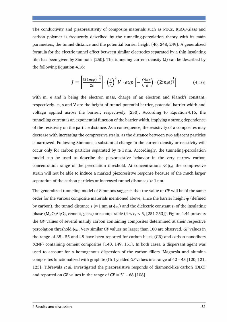
4 Results and discussion 81
The conductivity and piezoresistivity of composite materials such as PDCs, RuO2/Glass and
carbon polymer is frequently described by the tunneling-percolation theory with its main
parameters, the tunnel distance and the potential barrier height [46, 248, 249]. A generalized
formula for the electric tunnel effect between similar electrodes separated by a thin insulating
film has been given by Simmons [250]. The tunneling current density (J) can be described by
the following Equation 4.16:
𝐽 = [3(2𝑚𝜑)−
12
2𝑠] ∙ (
𝑒
ℎ)2𝑉 ∙ 𝑒𝑥𝑝 [−(
4𝜋𝑠
ℎ) ∙ (2𝑚𝜑)
1
2] (4.16)
with m, e and h being the electron mass, charge of an electron and Planck’s constant,
respectively. φ, s and V are the height of tunnel potential barrier, potential barrier width and
voltage applied across the barrier, respectively [250]. According to Equation 4.16, the
tunnelling current is an exponential function of the barrier width, implying a strong dependence
of the resistivity on the particle distance. As a consequence, the resistivity of a composites may
decrease with increasing the compressive strain, as the distance between two adjacent particles
is narrowed. Following Simmons a substantial change in the current density or resistivity will
occur only for carbon particles separated by ≲ 1 nm. Accordingly, the tunneling-percolation
model can be used to describe the piezoresistive behavior in the very narrow carbon
concentration range of the percolation threshold. At concentrations ≪ cri. the compressive
strain will not be able to induce a marked piezoresistve response because of the much larger
separation of the carbon particles or increased tunnel distances ≫ 1 nm.
The generalized tunneling model of Simmons suggests that the value of GF will be of the same
order for the various composite materials mentioned above, since the barrier height φ (defined
by carbon), the tunnel distance s (≈ 1 nm at cri.) and the dielectric constant εr of the insulating
phase (MgO,Al2O3, cement, glass) are comparable (4 < εr < 5, [251-253]). Figure 4.44 presents
the GF values of several mainly carbon containing composites determined at their respective
percolation threshold cri.. Very similar GF values no larger than 100 are observed. GF values in
the range of 38 – 55 and 48 have been reported for carbon black (CB) and carbon nanofibers
(CNF) containing cement composites [140, 149, 151]. In both cases, a dispersant agent was
used to account for a homogenous dispersion of the carbon fillers. Magnesia and alumina
composites functionalized with graphite (Gr.) yielded GF values in a range of 42 – 45 [120, 121,
123]. Tibrewala et al. investigated the piezoresistive responds of diamond-like carbon (DLC)
and reported on GF values in the range of GF = 51 – 68 [108].

82 4 Results and discussion
Figure 4.44: GF (at the respective cri.) of inorganic nano-composites, with = [140], = [120, 121],
▷ = [46], = [149, 151] and = [108, 109].
For the sake of comparison the GF values of PDC materials from the literature (diamond
symbols) and the GF value for C-11 (our value closest to C) are included in Figure 4.44.
Evidently, these GF values reported on PDCs do not fit into this classification and will be
discussed in chapter 4.4.4.
4.4.2 Effect of temperature on the piezoresistive behavior
In the following, the temperature dependency of the GF value of C-11 prepared at T = 1600 °C
is presented and compared to literature [166]. Two different measurement setups have been
used for the thermal investigations. In the low-temperature region (T < 400 °C) the electrical
contacts are oriented perpendicular to the strain direction whereas in the high-temperature
region (T > 1000 °C) the compressive strain was applied directly onto the contacted front
surface (Figure 3.2).
Within the temperature range RT < T < 400 °C the GF is almost constant. The Arrhenius plot
yields an activation energy of about 0.01 ± 5∙10-3 eV, as depicted in Figure 4.45. The very low
activation energy suggests that GF is either correlated with a weakly temperature dependent
carrier mobility or a weak change of the carrier density. According to the Hall measurements of
C-11 both quantities change very slightly within the temperature range given above (2.6 to
1.4 cm²/Vs and 7∙10-17 to 1∙10-18 cm-3) allowing no unambiguous decision which quantity
determines the temperature dependence of GF.
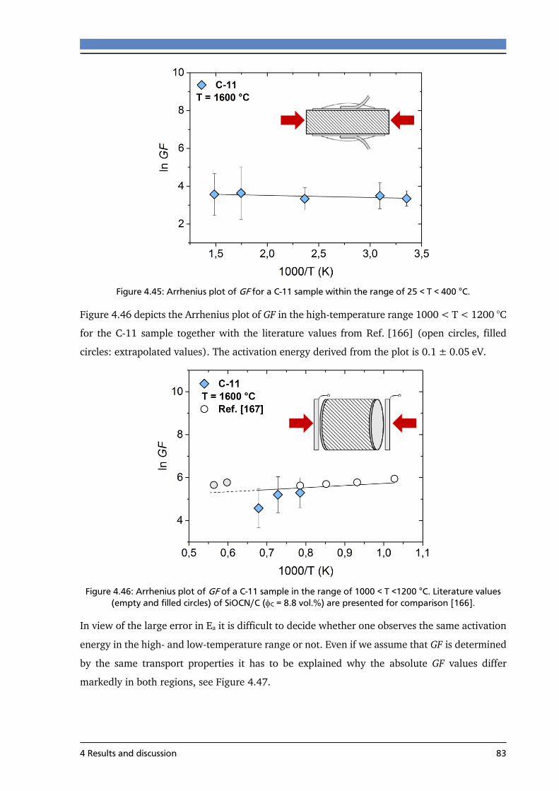
4 Results and discussion 83
Figure 4.45: Arrhenius plot of GF for a C-11 sample within the range of 25 < T < 400 °C.
Figure 4.46 depicts the Arrhenius plot of GF in the high-temperature range 1000 < T < 1200 °C
for the C-11 sample together with the literature values from Ref. [166] (open circles, filled
circles: extrapolated values). The activation energy derived from the plot is 0.1 ± 0.05 eV.
Figure 4.46: Arrhenius plot of GF of a C-11 sample in the range of 1000 < T <1200 °C. Literature values
(empty and filled circles) of SiOCN/C (C = 8.8 vol.%) are presented for comparison [166].
In view of the large error in Ea it is difficult to decide whether one observes the same activation
energy in the high- and low-temperature range or not. Even if we assume that GF is determined
by the same transport properties it has to be explained why the absolute GF values differ
markedly in both regions, see Figure 4.47.

84 4 Results and discussion
Figure 4.47: GF values of the two temperature regimes. Literature values (empty and filled circles) of
SiOCN/C (C = 8.8 vol.%) are presented for comparison [165].
A possible explanation is the following. As described above two different measurement
techniques have been applied: in the high-temperature experiment compressive strain is applied
to the contacts at the front surfaces whereas at low temperature only the strain in the bulk
(bulk) determines the piezoresistive effect. The observed discontinuous change in GF may
therefore arise from the different local strain distributions at the sample/electrode interfaces.
Figure 4.48: Schematic depiction of the local strain at the sample/electrode interface during loading.
Agreement between the two measurements can then be obtained if the (local) strain in the
electrode region of the high-temperature setup is approximately one magnitude higher than the
apparent strain applied. Hence, the local strain will be given by:
𝜀𝑙𝑜𝑐𝑎𝑙 = ∙ 𝜀𝑏𝑢𝑙𝑘 (4.17)
with the enhancement factor. The enhancement factor will depend on the surface roughness
in the sample/electrode interface. The rougher the surface the more contact points will be
present raising the strain in the interface.

4 Results and discussion 85
4.4.3 Origin of the piezoresistve effect in SiOC/C
The change of the resistance with strain in SiOC/C composites will depend on three factors: the
charge carrier mobility µ and density N and the geometrical change. The latter can be neglected
due to the high stiffness of the material (E ≈ 100 GPa, [254]). The resistance generally scales
with 1/µ and 1/N. Experimentally, one observes that the resistance decreases with strain (and
temperature). Hence, the origin of the piezoresistive effect will be either an increase in µ or N.
For (isotropic) condensed matter the dispersion relation E(k) remains linear in the presence of
strain.
𝐸(𝑘) = ℎ𝐹(𝜖) ∙ 𝑘 (4.18)
Where h is the Planck constant, k the wave factor and F the Fermi velocity that depends on the
strain . At a given energy E(k) the magnitude of k is larger for strained materials than in relaxed
materials. Accordingly, the density of states has to increase with strain because it is
approximately proportional to the inverse of the squared fermi velocity:
𝑁(𝜖)~1
𝐹(𝜖)² (4.19)
An increase of the carrier density leads to a decrease of the resistance as observed in our
piezoresistive measurements: the origin of the piezoresistive effect therefore would be the
strain-induced change of the density of states near EF. A change of the mobility is unable to
explain the experimental results. Assuming again that the Fermi velocity decreases with strain
and that F scales with µ, the mobility will decrease leading to an increase of the resistance with
strain which is not observed. However, both quantities may change with strain. In order to be
consistent with the experimental results the change in the carrier density has to outweigh the
mobility change. Further experimental and theoretical work are needed to give a unique
explanation for the piezoresistive effect in SiOC/C.
4.4.4 Comment on giant gauge factors in PDCs reported in literature
As shown in Figure 4.44 GF values of about 200 to 2000 exist for PDCs with typical carbon
concentration between 8 to 11 vol.% which differ substantially from the values obtained in this
work with the configuration depicted in Figure 3.2a).
Thin film resistors (TFR) and silicon nanowires are the two main systems in which enhanced
gauge factors are commonly observed. In both cases stress concentration is held to be
responsible for the observed effect i.e., the local strain is enhanced with respect to the averaged
macroscopic strain [255, 256]. According to Ref. [255] GF enhancement occurs in

86 4 Results and discussion
(heterogeneous) thin film resistors when: the conducting phase is stiffer than the glassy one
and when the size of the spatially separated conducting particles is much larger than the
tunneling distance. Both requirements are fulfilled for polymer-derived materials close to the
percolation threshold indicating that the strain distribution in the interface region between the
conductive filler(carbon)/glassy matrix determines the GF enhancement. In case of silicon
nanowires the GF changes with the chemical treatment of the wires. The enhancement of GF is
expressed as:
𝐺𝐹𝑒𝑛ℎ𝑎𝑛𝑐𝑒𝑑 = ∙ 𝐺𝐹𝑏𝑢𝑙𝑘 (4.20)
similar in magnitude to the bulk effect and related to geometric (local) stress concentration. In
this work mainly SiOC/C samples with carbon concentrations above the percolation threshold
have been investigated. In this case, no conducting carbon particles remaining suspended in the
matrix have to be considered but a continuous carbon network within a glassy matrix. Hence,
the strain distribution within such composites will differ from that of the above mentioned
composites close to the percolation threshold. Generally, the local strain within the sample and
the local strain within the interface electrode/sample region contribute to the GF enhancement.
If the local stress within the sample is small and negligible the stress distribution in the interface
dominates changing markedly when compressive stress in applied. As suggested in Figure 4.48
the local stress will decline with declining surface roughness and vanish for plain surfaces. Such
a behavior is observed for, e.g., sample C-11 (Figure 4.49) when the sample is contacted
according to Figure 3.2b).
Figure 4.49: Gauge factor as a function of the applied pressure of a C-11 sample.

4 Results and discussion 87
For low compressive stress (0.5 - 3 MPa) GF corresponds to values around 500 - 3500. When
increasing the stress to 5 - 10 MPa GF decreases to about 145 due to the declining of the local
strain and approaches the bulk value, GFbulk ≈ 70, determined with the contact geometry
depicted in Figure 3.2a).
4.4.5 Development and application of a SiOC/C based prototype
The urgent need of the automotive and aircraft industry for sensing over a broader temperature
range up to T = 500 °C have been expressed several times and have led to extensive effort to
develop high-temperature sensor materials [257, 258]. Currently, piezoelectric materials are
widely used in commercially available sensors which often suffer from the loss of their
piezoelectric properties at temperatures above T > 200 – 300 °C [259]. The increased thermal
stability of the SiOC/C ceramic, however, meets the industrial requirements and thus makes it
a promising candidate material for future sensing at elevated temperatures (T > 400 °C).
A first sensor prototype based on a C-17 sample was developed in cooperation with the institute
of Electromechanical Design at the TU Darmstadt and the department of Energy and
Automation technology at the TU Berlin for RT measurements. A schematic depiction of the
developed sensor is given in Figure 4.50. The sensor consist of a base plate connected to an
initial load element. The piezoresistive SiOC/C is polished in rectangular shape (3x3x10 mm)
and clamped between the base and the load element. As the screws are tightened, the load
element is pressed against the base applying the required preload of P = 10 MPa. Apart from
holding the SiOC/C material in place, the springs also minimize the danger of tilting upon
tightening. The electrical contacts are located on the long side of the sample and thus are not
affected by the applied preload. To investigate the dynamic piezoresistive behavior a planetary
gear was constructed at the TU Berlin given in Figure 4.51.
Figure 4.50: Schematic depiction of the piezoresistive SiOC/C sensor prototype for RT measurements.
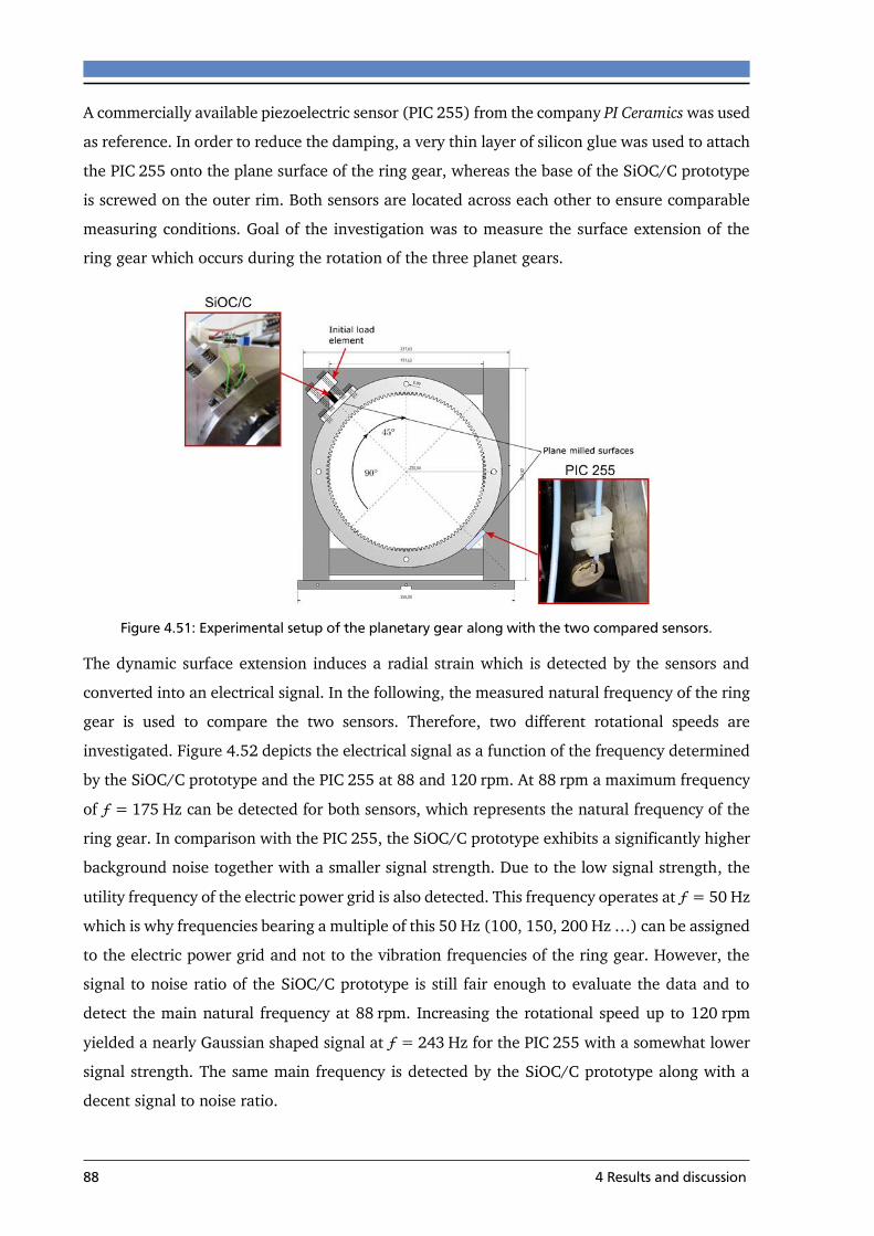
88 4 Results and discussion
A commercially available piezoelectric sensor (PIC 255) from the company PI Ceramics was used
as reference. In order to reduce the damping, a very thin layer of silicon glue was used to attach
the PIC 255 onto the plane surface of the ring gear, whereas the base of the SiOC/C prototype
is screwed on the outer rim. Both sensors are located across each other to ensure comparable
measuring conditions. Goal of the investigation was to measure the surface extension of the
ring gear which occurs during the rotation of the three planet gears.
Figure 4.51: Experimental setup of the planetary gear along with the two compared sensors.
The dynamic surface extension induces a radial strain which is detected by the sensors and
converted into an electrical signal. In the following, the measured natural frequency of the ring
gear is used to compare the two sensors. Therefore, two different rotational speeds are
investigated. Figure 4.52 depicts the electrical signal as a function of the frequency determined
by the SiOC/C prototype and the PIC 255 at 88 and 120 rpm. At 88 rpm a maximum frequency
of ƒ = 175 Hz can be detected for both sensors, which represents the natural frequency of the
ring gear. In comparison with the PIC 255, the SiOC/C prototype exhibits a significantly higher
background noise together with a smaller signal strength. Due to the low signal strength, the
utility frequency of the electric power grid is also detected. This frequency operates at ƒ = 50 Hz
which is why frequencies bearing a multiple of this 50 Hz (100, 150, 200 Hz …) can be assigned
to the electric power grid and not to the vibration frequencies of the ring gear. However, the
signal to noise ratio of the SiOC/C prototype is still fair enough to evaluate the data and to
detect the main natural frequency at 88 rpm. Increasing the rotational speed up to 120 rpm
yielded a nearly Gaussian shaped signal at ƒ = 243 Hz for the PIC 255 with a somewhat lower
signal strength. The same main frequency is detected by the SiOC/C prototype along with a
decent signal to noise ratio.

4 Results and discussion 89
Figure 4.52: Natural frequency of the ring gear measured at 88 and 120 rpm using the SiOC/C prototype
and a commercially available PIC 255 sensor.
In general, a low electrical resistivity is desirable in sensing measurements since the low
electrical resistivity is helpful for enhancing the signal to noise ratio. However, a low resistivity
impairs the piezoresistive behavior of the SiOC/C material. Fortunately, there is a balance
between a decent piezoresistive effect and low electrical resistivity near the percolation
threshold. Thus, the percolation threshold is an important parameter for designing and further
optimizing the sensing property of the SiOC/C material.
In summary it can be stated that, in a first attempt the SiOC/C based prototype has proven its
worth in both rotation ranges as a useful sensor to detect the main natural frequency of the ring
gear. Together with a suitable downstreamed electronic filter (low-pass and/or band pass filter)
and an adjusted composition closer to the percolation threshold, the sensitivity can be further
increased and might even be used in future to detect early abrasion or even crack formation of
the cogs. Furthermore, does the thermal stability of the material allows for sensing at elevated
temperatures in contrast to the commercially available piezoelectric sensor materials. To further
improve the sensibility of the sensor the electrical resistance should be assessed using a
four-point method instead of a two-point method. This would allow to fully exclude the lead
and contact resistance from the measurement as separated electrodes for current and voltage

90 4 Results and discussion
are used. Hence, the SiOC/C material can be considered a promising future sensor material for
sensing at elevated temperatures (T > 400 °C).
4.4.6 Summary
Two different experimental setups have been developed to determine the gauge factor GF of
SiOC/C in compressive mode after preloading. The latter proved to be essential to achieve
reliable gauge factors for the bulk material needed for strain sensing applications (for
demonstration a radial strain sensor has been developed in this work).
As in other carbon based materials the GF of SiOC/C prepared at T = 1600 °C seems to depend
on the concentration of point or extended defects. As supported by the Raman data the defect
density increases with decreasing amount of carbon and, accordingly, GF increases steadily
within the range of 36 to 17 vol.% carbon (GFC-36 = 3, GFC-17 = 45). Within this concentration
range the piezoresistive behavior appears to be related to strain-induced changes of the density
of states near EF. A change in mobility is unable to explain the experimental result.
A very similar increase in GF up to about 50 occurs at low carbon concentration in the range of
6 to 11 vol.% carbon. Whether GF diverges at the percolation threshold (cri. ≈ 6 ± 2 vol.%), as
expected from percolation-tunneling theory, or reaches a maximum in the range of 11 to
17 vol.% carbon, remains unclear and needs further investigations.
Divergence of GF at the percolation threshold may explain the extremely high GFs, reported in
literature for other PDCs. However, giant GF values may also originate from local strain
concentration, with local deviating from bulk by an enhancement factor . In order to explain
these literature data has to reach values ≫ 10².

5 Conclusion & Outlook 91
5 Conclusion & Outlook
Within the thesis, the state of carbon in SiOC/C and its piezoresistive effect have been
investigated. Polymer-derived SiOC/C ceramics with different amount of carbon
(C =1 - 46 vol.%) have been synthesized by pyrolysis of poly-organosiloxane networks and
subsequent spark plasma sintering at different temperatures (1000 < T < 1800 °C). The
morphological and electrical properties of carbon within SiOC/C mainly depend on the actual
carbon concentration and the synthesis temperature which determines the stage of
graphitization. In case of samples with very low carbon content (C ≲ 1 vol.%) carbon remains
isolated in the glassy matrix and accordingly the electrical transport is limited by localized states
in the matrix. With increasing synthesis temperature the structural order within carbon changes
from a disordered amorphous to a nano-crystalline state as proven by UV Raman studies. The
change/ordering tendency from the amorphous to the crystalline state is reflected by the
decrease of the Raman D band and the simultaneous increase of the Raman G band. Their
intensity ratio AD/AG is generally accepted as a measure of the graphitization progress and
allows to assess the lateral crystal size (La) and the average defect distance (LD) in carbon. In
SiOC/C La stays constant (7.5 nm) up to T = 1500 °C and starts to rapidly increase above this
temperature indicating expansion of the graphitic layer size or increasing ordering, respectively.
The latter is also seen in LD which increases from about 6 nm (T = 1000 °C) to 12.5 nm
(T = 1800 °C). As LD ~ 1/Ndef. the defect density decreases with temperature as expected for
ongoing crystallization. Vacancies have been identified as main type of defect in nano-
crystalline graphite.
Concerning the electrical and piezoresistive properties of SiOC/C the experimental work has
been focused on samples prepared at T = 1600 °C. The main advantage of this way of
proceeding is that only one well-defined type of carbon (nano-crystalline carbon) has to be
considered which forms a continuous three-dimensional graphitic network at a carbon
concentration ≳ 6 vol.%, i.e., at the percolation threshold cri.. Above cri. electrical transport
occurs within conjugated bonds and is only weakly activated (Ea < 0.03 eV) like in glassy
carbon. Below cri. semiconducting behavior is observed for carbon concentration of about 2 to
6 vol.% indicated by an activation energy of Ea ≈ 0.3 eV and charge carrier densities of N = 1015
to 1018 cm-³. The transport mechanism changes from band-like transport to conduction via
localized states which very likely arise from electron/hole confinement when the localization
length approaches a lateral crystal size less than 10 nm as derived from Raman measurements.
SiOC/C changes its resistivity upon applying a strain and, accordingly, the piezoresistive effect
also relies on the carbon concentration and the degree of ordering within carbon. Close to/at

92 5 Conclusion & Outlook
the percolation threshold the gauge factor (GF) can be explained by charge carrier tunnelling.
At this concentration rather high GF values are observed which, according to theory, originates
from divergence at cri. or local stress concentration. Above cri. GF appears to be related to the
density of defects within the carbon network. A change in mobility is unable to explain the
experimental results.
Future work should concentrate on the following topics:
(i) investigation of the piezoresistivity of samples synthesized at 1100 and 1400 °C to complete
the results on the 1600 °C samples.
(ii) 4-point measurements of the resistivity at high-temperatures (T > 400 °C) to check/exclude
the strain contribution from the interface electrode/sample.
(iii) modelling of the strain distribution and study of the interface carbon/glassy matrix to
determine possible effects on the electrical properties.
(iv) long-term stability as an essential requirement for sensor development.
(v) thermally stable packaging of the sensor electronics including reduction of the background
noise by a suitable electronic filter.

6 References 93
6 References
1. Fritz G. and Raabe B., Z. Anorg. Allg. Chem., 286(3-4), 149-167, 1956. 2. Ainger F. W. and Herbert J. M., The preparation of Phosphorus-Nitrogen Compounds as
Non-Porous Solids, in Special Ceramics, 1960, Academic Press: New York.
3. Chantrell P. G. and Popper P., Inorganic Polymers for Ceramics, in Special Ceramics,
1965, Academic Press: New York.
4. Verbeek W., Ger. Pat. No. 2218960, 1973.
5. Verbeek W. and Winter G., Ger. Pat. No. 2236078, 1974. 6. Winter G., Verbeek W., and Mansmann M., Ger. Pat. No. 2243527, 1974.
7. Yajima S., Okamura K., Hayashi J., and Omori M., J. Am. Ceram. Soc., 59(7-8), 324-327,
1976.
8. Yajima S., Hayashi J., Omori M., and Okamura K., Nature, 261(5562), 683-685, 1976.
9. Yajima S., Hasegawa Y., Hayashi J., and Iimura M., J. Mater. Sci., 13(12), 2569-2576,
1978.
10. Diré S., Babonneau F., Sanchez C., and Livage J., J. Mater. Chem., 2(2), 239-244, 1992.
11. Soraru G. D., Mercadini M., Maschio R. D., Taulelle F., et al., J. Am. Ceram. Soc., 76(10),
2595-2600, 1993.
12. Wootton A. M., Rappensberger M., Lewis M. H., Kitchin S., et al., J. Non-Cryst. Solids,
204(3), 217-227, 1996.
13. Riedel R., Kienzle A., Dressler W., Ruwisch L., et al., Nature, 382(6594), 796-798, 1996.
14. Riedel R., Ruswisch L. M., An L., and Raj R., J. Am. Ceram. Soc., 81(12), 3341-3344,
1998.
15. Ionescu E., Linck C., Fasel C., Müller M., et al., J. Am. Ceram. Soc., 93(1), 241-250, 2010.
16. Ionescu E., Papendorf B., Kleebe H.-J., Poli F., et al., J. Am. Ceram. Soc., 1782(6), 1774-
1782, 2010.
17. Ionescu E., Papendorf B., Kleebe H.-J., and Riedel R., J. Am. Ceram. Soc., 1789, 1783-
1789, 2010.
18. Riedel R., Mera G., Hauser R., and Klonczynski A., J. Ceram. Soc. Jpn., 114(1330), 425-444, 2006.
19. Colombo P., Mera G., Riedel R., and Soraru G. D., J. Am. Ceram. Soc., 93(7), 1805-1837,
2010.
20. Kleebe H.-J. and Blum Y. D., J. Eur. Ceram. Soc., 28(5), 1037-1042, 2008.
21. Bodet R., Jia N., and Tressler R. E., J. Eur. Ceram. Soc., 16(6), 653-664, 1996. 22. Ellis R. B., U.S. Pat. No. 2,556,616, 1951.
23. Smith C. F. and Crandall W. B., U.S. Pat. No. 3,378,431, 1968.
24. Pantano C. G., Singh A. K., and Zhang H. X., J. Sol-Gel Sci. Technol., 14(1), 7-25, 1999.
25. Elmer T. H. and Meissner H. E., J. Am. Ceram. Soc., 59(5-6), 206-209, 1976. 26. Pampuch R., Ptak W. S., Jonas S., and Stoch J., The nature of Si-O-C phase(s) formed
during oxidation of SiC, in Proceeding of the 9th International Symposium on Reactivity
of Solids, Cracow, Poland, 1980, Elsevier: New York.
27. Lipowitz J., Freeman H. A., Chen R. T., and Prack E. R., Adv. Ceram. Mater., 2(2), 121-128, 1987.
28. Lipowitz J., Am. Ceram. Soc. Bull., 70(12), 1888-1894, 1991.
29. Porte L. and Sartre A., J. Mater. Sci., 24(1), 271-275, 1989.
30. Saha A., Raj R., and Williamson D. L., J. Am. Ceram. Soc., 89(7), 2188-2195, 2006.
31. Widgeon S. J., Sen S., Mera G., Ionescu E., et al., Chem. Mater., 22(23), 6221-6228, 2010.
32. Saha A. and Raj R., J. Am. Ceram. Soc., 90(2), 578-583, 2007.
33. Mera G., Navrotsky A., Sen S., Kleebe H. J., et al., J. Mater. Chem. A, 1(12), 3826-3836, 2013.

94 6 References
34. Monthioux M. and Delverdier O., J. Eur. Ceram. Soc., 16(7), 721-737, 1996.
35. Bréquel H., Parmentier J., Sorarù G. D., Schiffini L., et al., Nanostruct. Mater., 11(6),
721-731, 1999.
36. Kleebe H.-J., Turquat C., and Sorarù G. D., J. Am. Ceram. Soc., 84(5), 1073-1080, 2001.
37. Papendorf B., Ionescu E., Kleebe H.-J., Linck C., et al., J. Am. Ceram. Soc., 96(1), 272-
280, 2013.
38. Bunde A. and Dieterich W., J. Electroceram., 5(2), 81-92, 2000.
39. Kirkpatrick S., Rev. Mod. Phys., 45(4), 574-588, 1973.
40. McLachlan D. S., Blaszkiewicz M., and Newnham R. E., J. Am. Ceram. Soc., 73(8), 2187-
2203, 1990.
41. Essam J. W., Rep. Prog. Phys., 43(7), 833-912, 1980.
42. Bruggeman D. A. G., Annalen der Physik, 416(7), 636-664, 1935.
43. Rozen J., Lopez R., Haglund R. F., and Feldman L. C., Appl. Phys. Lett., 88(8), 081902, 2006.
44. Batrouni G. G., Hansen A., and Larson B., Phys. Rev. E, 53(3), 2292-2297, 1996.
45. Clerc J. P., Podolskiy V. A., and Sarychev A. K., Eur. Phys. J. B, 15(3), 507-516, 2000.
46. Vionnet-Menot S., Grimaldi C., Maeder T., Strässler S., et al., Phys. Rev. B, 71(6),
064201-064201, 2005.
47. Balberg I. I., Phys. Rev. Lett., 59(12), 1305-1308, 1987.
48. Balberg I., Phys. Rev. B, 57(21), 13351-13354, 1998.
49. Cordelair J. and Greil P., J. Eur. Ceram. Soc., 20(12), 1947-1957, 2000.
50. Martinez-Crespiera S., Ionescu E., Kleebe H. J., and Riedel R., J. Eur. Ceram. Soc., 31(5), 913-919, 2011.
51. Haluschka C., Engel C., and Riedel R., J. Eur. Ceram. Soc., 20(9), 1365-1374, 2000.
52. Kim K. J., Eom J.-H., Kim Y.-W., and Seo W.-S., J. Eur. Ceram. Soc., 35(5), 1355-1360, 2015.
53. Nguyen V. L., Zanella C., Bettotti P., and Sorarù G. D., J. Am. Ceram. Soc., 97(8), 2525-
2530, 2014.
54. Chung D. D. L., J. Mater. Sci., 37(8), 1475-1489, 2002.
55. Jenkins G. M. and Kawamura K., Polymeric carbons - carbon fiber, glass and char, in,
1976, Cambridge University Press Cambridge. .
56. Li L., Zhu Z. H., Lu G. Q., Yan Z. F., et al., Appl. Catal. A Gen., 309(2), 201-209, 2006.
57. Ergun S. and Alexander L. E., Nature, 195(4843), 765-767, 1962.
58. Kakinoki J., Komura Y., and Ino T., Acta Crystallogr., 13(3), 171-179, 1960.
59. Jenkins G. M. and Kawamura K., Nature, 231(5299), 175-6, 1971.
60. Ergun S., Carbon, 14(3), 139-150, 1976.
61. Stenhouse B. J. and Grout P. J., J. Non-Cryst. Solids, 27(2), 247-256, 1978.
62. Beeman D., Silverman J., Lynds R., and Anderson M. R., Phys. Rev. B, 30(2), 870-875, 1984.
63. Robertson J. and O'Reilly E. P., Phys. Rev. B, 35(6), 2946-2957, 1987.
64. Robertson J., Adv. Phys., 35(4), 317-374, 1986.
65. Jansen F., Machonkin M., Kaplan S., and Hark S., J. Vac. Sci. Technol., A, 3(3), 605-609, 1985.
66. Dischler B., Appl. Phys. Lett., 42(8), 636, 1983.
67. Teo K. B. K., Ferrari A. C., Fanchini G., Rodil S. E., et al., Diamond Relat. Mater., 11(3-6), 1086-1090, 2002.
68. Veerasamy V. S., Amaratunga G. A. J., Davis C. A., Timbs A. E., et al., J. Phys.: Condens.
Matter, 5(13), L169-L174, 1993.
69. Neuville S., QSci. Connect, 8, 2-27, 2014.
70. Jungnickel G., Frauenheim T., Porezag D., Blaudeck P., et al., Phys. Rev. B, 50(10), 6709,
1994.
6 References 95
71. Krüger A., Neue Kohlenstoffmaterialien: Eine Einführung 2007, Teubner Verlag / GWV
Fachverlage GmbH: Wiesbaden.
72. Issi J.-P. and Charlier J.-C., Electrical Transport Properties in Carbon Nanotubes, in The
Science and Technology of Carbon Nanotubes, 1999, Elsevier Science Ltd.: Oxford. 73. Moore A. W., Physics and Chemistry of Carbon, 1973, Dekker: New York
74. Clark C. D., Dean P. J., and Harris P. V., Proc. R. Soc. Lon. Ser. A, 277(1370), 312-315,
1964.
75. Short M. A. and Walker P. L., Carbon, 1(1), 3-9, 1963.
76. Noda T., Inagaki M., and Yamada S., J. Non-Cryst. Solids, 1, 285-302, 1969.
77. Franklin R. E., Proc. R. Soc. Lon. Ser. A, 209(1097), 196-&, 1951.
78. Morgan M., Thin Solid Films, 7(5), 313-323, 1971.
79. Schwan J., Ulrich S., Batori V., Ehrhardt H., et al., J. Appl. Phys., 80(1), 440-440, 1996.
80. Davis C. A., Silva S. R., Dunin-Borkowski R. E., Amaratunga G. A., et al., Phys. Rev. Lett.,
75(23), 4258-4261, 1995.
81. Dasgupta D., Demichelis F., and Tagliaferro A., Philos. Mag. B, 63(6), 1255-1266, 1991.
82. Riedel E. and Janiak C., Anorganische Chemie, 2007, De Gruyter: Berlin.
83. Anderson P. W., Phys. Rev., 109(5), 1492-1505, 1958.
84. Mott N. F., Philos. Mag., 17(150), 1259-1268, 1968.
85. Cohen M. H., Fritzsche H., and Ovshinsky S. R., Phys. Rev. Lett., 22(20), 1065-1068, 1969.
86. Davis E. A. and Mott N. F., Philos. Mag., 22(179), 0903-0922, 1970.
87. Mott N. F. and Davis E. A., Electronic processes in non-crystalline materials, 1979,
Clarendon Press: Oxford.
88. Liu C.-C., Walters A. B., and Vannice M. A., Carbon, 33(12), 1699-1708, 1995.
89. Dresselhaus M. S., Dresselhaus G., Sugihara K., Spain I. L., et al., Graphite Fibers and Filaments, 1988, Springer-Verlag: Berlin, Heidelberg.
90. Klein C. A., Rev. Mod. Phys., 34(1), 56-79, 1962.
91. Mrozowski S., Phys. Rev., 85(4), 609-620, 1952.
92. Soule D. E. and McCluke J. W., J. Phys. Chem. Solids, 8, 29-35, 1959.
93. Galt J. K., Yager W. A., and Dail H. W., Phys. Rev., 103(5), 1586-1587, 1956.
94. Cookson J. W., Phys. Rev., 47(2), 194-195, 1935.
95. Eisler P., US 2,885,524, 1959.
96. Jackson P. G. S., GB 720,325, 1952.
97. Bardeen J. and Shockley W., Phys. Rev., 80(1948), 72-80, 1950.
98. Smith C. S., Phys. Rev., 919, 1954.
99. Mason W. P. and Thurston R. N., J. Acous. Soc. Am., 29(10), 1096-1101, 1957.
100. Herring C. and Vogt E., Phys. Rev., 101, 944-961, 1956.
101. Rowe A. C. H., J. Mater. Res., 29(06), 731-744, 2014.
102. Baykan M. O., Thompson S. E., and Nishida T., J. Appl. Phys., 108(9), 2010. 103. Chaparala M. V. and Shivaram B. S., Piezoresistance of c-Si, in Properties of Crstalline
Silicon, 1998, The Institution of Electrical Engineers: London, United Kingdom.
104. Kanda Y., IEEE Trans. Electron Devices, 29(1), 64-70, 1982.
105. Barlian a. A., Park W.-T., Mallon J. R., Rastegar A. J., et al., Proceedings of the IEEE.
Institute of Electrical and Electronics Engineers, 97(3), 513-552, 2009.
106. Curtis G. J., Milne J. M., and Reynolds W. N., Nature, 220(5171), 1024-1025, 1968.
107. Peiner E., Tibrewala A., Bandorf R., Biehl S., et al., Sensors and Actuat. A-Phys., 130, 75-82, 2006.
108. Tibrewala A., Peiner E., Bandorf R., Biehl S., et al., J. Micromech. Microeng., 17(7), S77-
S82, 2007.
109. Tibrewala a., Peiner E., Bandorf R., Biehl S., et al., Mater. Sci. Technol., 23(3), 362-367, 2007.
110. Wang Y., Yang R., Shi Z., Zhang L., et al., ACS Nano, 5(5), 3645-50, 2011.

96 6 References
111. Hosseinzadegan H. and Todd C. Graphene has ultra high piezoresistive gauge factor, in
IEEE 25th International Conference on Micro Electro Mechanical Systems (MEMS),
2012,
112. Lee Y., Bae S., Jang H., Jang S., et al., Nano Lett., 10(2), 490-3, 2010.
113. Bae S.-H., Lee Y., Sharma B. K., Lee H.-J., et al., Carbon, 51, 236-242, 2013.
114. Huang M., Pascal T. A., Kim H., Goddard W. A., et al., Nano Lett., 11(3), 1241-6, 2011.
115. Pereira V. M., Castro Neto A. H., Liang H. Y., and Mahadevan L., Phys. Rev. Lett., 105(15), 156603, 2010.
116. Ni Z. H., Yu T., Lu Y. H., Wang Y. Y., et al., ACS Nano, 2(11), 2301-5, 2008.
117. Zhao J., He C., Yang R., Shi Z., et al., Appl. Phys. Lett., 101(6), 063112-063112, 2012.
118. Camargo P. H. C., Satyanarayana K. G., and Wypych F., Materials Research, 12(1), 1-39,
2009.
119. Liew L. A., Zhang W., An L., Shah S., et al., Am. Ceram. Soc. Bull., 80(5), 25-30, 2001.
120. Waku K., Hayashi H., and Kishimoto A., J. Am. Ceram. Soc., 91(12), 4168-4170, 2008.
121. Waku K., Tagaya S., Hayashi H., and Kishimoto A., J. Ceram. Soc. Jpn., 117(1367), 793-796, 2009.
122. Stauffer D. and Aharony A., Introduction to percolation Theory, 1994, Taylor & Francis
Group: Philadelphia.
123. Kishimoto A., Takagawa Y., Teranishi T., and Hayashi H., Mater. Lett., 65(14), 2197-2200, 2011.
124. Auerkari P., Mechanical and physical properties of engineering alumina ceramics, VTT
Manufacturing Technology, 1996, Technical Research Centre of Finland (VTT):
Finland.
125. Riedel R. and Chen I. W., Ceramics Science and Technology, Materials and Properties,
2010, WILEY-VCH Verlag GmbH & Co. KGaA: Weinheim.
126. Chen P.-W. and Chung D. D. L., Smart Mater. Struct., 2(1), 22-30, 1993.
127. Shao-peng W., Lian-tong M., Zhong-he S., Dong-xing X., et al., Journal of Wuhan
University of Technology-Mater. Sci. Ed., 17(4), 69-72, 2002.
128. Monfore G. E., J. PCA Res. Dev. Lab., 10(2), 35-48, 1968.
129. Wen S. and Chung D. D. L., Carbon, 45(3), 505-513, 2007.
130. Pan P., Wu S., Xiao F., Pang L., et al., J. Intell. Mater. Syst. Struct., 2014.
131. Wen S. and Chung D. D. L., Carbon, 44(8), 1496-1502, 2006.
132. Xiao H., Li H., and Ou J., J. Intell. Mater. Syst. Struct., 22(2), 191-200, 2011.
133. Fu X. L. and Chung D. D. L., Cem. Concr. Res., 26(1), 15-20, 1996.
134. Chen P.-W. and Chung D. D. L., J. Am. Ceram. Soc., 78(3), 816-818, 1995.
135. Wang S., Shui X., Fu X., and Chung D. D. L., J. Mater. Sic., 33(15), 3875-3884, 1998.
136. Yao W., Chen B., and Wu K., Chem. Phys, 3, 3471-3471, 2001.
137. Wen S. and Chung D. D. L., Cem. Concr. Res., 31(2), 297-301, 2001.
138. Reza F., Batson G. B., Yamamuro J. A., and Lee J. S., J. Mater. Civ. Eng., 15(5), 476-483, 2003.
139. Chung D. D. L., J. Intell. Mater. Syst. Struct., 13(9), 599-609, 2002.
140. Galao O., Baeza F. J., Zornoza E., and Garcés P., Cem. Concr. Compos., 46, 90-98, 2014.
141. Howser R. N., Dhonde H. B., and Mo Y. L., Smart Mater. Struct., 20(8), 085031-085031,
2011.
142. Gao D., Sturm M., and Mo Y. L., Smart Mater. Struct., 20(4), 049501-049501, 2011.
143. Han B., Yu X., and Ou J., J. Mater. Sci., 45(14), 3714-3719, 2010.
144. Li G. Y., Wang P. M., and Zhao X., Cem. Concr. Compos., 29(5), 377-382, 2007.
145. Saafi M., Nanotechnology, 20(39), 395502-395502, 2009.
146. Yu X. and Kwon E., Smart Mater. Struct., 18(5), 055010-055010, 2009.
147. Li G. Y., Wang P. M., and Zhao X., Carbon, 43(6), 1239-1245, 2005.
148. Materazzi A. L., Ubertini F., and D’Alessandro A., Cem. Concr. Compos., 37, 2-11, 2013.
149. Li H., Xiao H., and Ou J., Cem. Concr. Compos., 28(9), 824-828, 2006.

6 References 97
150. Xiao H. G., Li H., and Ou J. P., Sensor Actuat. A-Phys., 160(1-2), 87-93, 2010.
151. Xiao H., Li H., and Ou J., Sensor Actuat. A-Phys., 167(2), 581-587, 2011.
152. Pang S. D., Gao H. J., Xu C., Quek S. T., et al. Strain and damage self-sensing cement composites with conductive graphene nanoplatelet, in Proceeding of SPIE, 2014, San
Diego
153. Ionescu E., Balan C., Kleebe H. J., Muller M. M., et al., J. Am. Ceram. Soc., 97(12), 3935-
3942, 2014.
154. Tyson B. M., Abu Al-Rub R. K., Yazdanbakhsh A., and Grasley Z., J. Mater. Civ. Eng.,
23(7), 1028-1035, 2011.
155. Wen S. and Chung D. D. L., Cem. Concr. Res., 36(10), 1879-1885, 2006.
156. Chung D. D. L., Adv Cem Res, 16(4), 167-176, 2004.
157. Han B. and Ou J., Sensor Actuat. A-Phys., 138(2), 294-298, 2007.
158. Ou J. and Han B., J. Intell. Mater. Syst. Struct., 20(3), 329-336, 2008.
159. Sáez de Ibarra Y., Gaitero J. J., Erkizia E., and Campillo I., Phys. Stat. Sol. A, 203(6), 1076-1081, 2006.
160. Zhang L., Wang Y., Wei Y., Xu W., et al., J. Am. Ceram. Soc., 91(4), 1346-1349, 2008.
161. Wang Y., Zhang L., Fan Y., Jiang D., et al., J. Mater. Sci., 44(11), 2814-2819, 2009.
162. Wang Y., Zhang L., Xu W., Jiang T., et al., J. Am. Ceram. Soc., 91(12), 3971-3975, 2008.
163. Wang Y., Ding J., Feng W., and An L., J. Am. Ceram. Soc., 94(2), 359-362, 2011.
164. Riedel R., Toma L., Janssen E., Nuffer J., et al., J. Am. Ceram. Soc., 93(4), 920-924, 2010.
165. Toma L., Kleebe H.-J., Müller M. M., Janssen E., et al., J. Am. Ceram. Soc., 95(29722),
1056-1061., 2012.
166. Terauds K., Sanchez-Jimenez P. E., Raj R., Vakifahmetoglu C., et al., J. Eur. Ceram. Soc., 30(11), 2203-2207, 2010.
167. Sorarù G. D., D'Andrea G., Campostrini R., Babonneau F., et al., J. Am. Ceram. Soc., 78(2), 379-387, 1995.
168. Rouxel T., Soraru G.-D., and Vicens J., J. Am. Ceram. Soc., 84(5), 1052-1058, 2001.
169. Ionescu E., Terzioglu C., Linck C., Kaspar J., et al., J. Am. Ceram. Soc., 96(6), 1899-1903, 2013.
170. Kaspar J., Graczyk-Zajac M., Choudhury S., and Riedel R., Electrochim. Acta, 216, 196-
202, 2016.
171. Kaspar J., Graczyk-Zajac M., and Riedel R., Solid State Ionics, 225, 527-531, 2012.
172. Renlund G. M., Prochazka S., and Doremus R. H., J. Mater. Res., 6(12), 2723-2734,
1991.
173. Sorarù G. D., J. Sol-Gel Sci. Technol., 2(1-3), 843-848, 1994.
174. Martínez-Crespiera S., Ionescu E., Kleebe H.-J., and Riedel R., J. Eur. Ceram. Soc., 31(5), 913-919, 2011.
175. Betz W., Shollenberger D., Keeler M., Buchanan M., et al. High Surface Area Graphitized
Mesoporous Carbons. 2007; Available from: http://www.sigmaaldrich.com/technical-
documents/articles/materials-science/nanomaterials/graphitized-mesoporous-
carbon.html.
176. Galusek D., Riley F. L., and Riedel R., J. Am. Ceram. Soc., 84(5), 1164-1166, 2001.
177. Rino J. P., Ebbsjö I., Branicio P. S., Kalia R. K., et al., Phys. Rev. B, 70(4), 045207, 2004.
178. Filsinger D. H. and Bourrie D. B., J. Am. Ceram. Soc., 73(6), 1726-1732, 1990.
179. Biernacki J. J. and Wotzak G. P., J. Am. Ceram. Soc., 72(1), 122-129, 1989. 180. Xue K., Niu L.-S., and Shi H.-J., Mechanical Properties of Amorphous Silicon Carbide, in
Silicon Carbide - Materials, Processing and Applications in Electronic Devices, 2011,
InTech
181. Esfehanian M., Oberacker R., Fett T., and Hoffmann M. J., J. Am. Ceram. Soc., 91(11),
3803-3805, 2008.
182. Plachký T., Lenč éš Z., Hric Ľ., Šajgalík P., et al., J. Eur. Ceram. Soc., 30(3), 759-767,
2010.

98 6 References
183. Kleebe H.-J., Gregori G., Babonneau F., Blum Y. D., et al., Z. Metallk., 97(6), 699-709, 2006.
184. Mazo M. a., Tamayo a., Rubio F., Soriano D., et al., J. Non-Cryst. Solids, 391, 23-31,
2014.
185. Bois L., Maquet J., Babonneau F., and Bahloul D., Chem. Mater., 7(5), 975-981, 1995.
186. Sousa B. F., Yoshida I. V. P., Ferrari J. L., and Schiavon M. A., J. Mater. Sci., 48(5), 1911-
1919, 2012.
187. Önneby C. and Pantano C. G., J. Vac. Sci. Technol., A, 15(3), 1597-1602, 1997.
188. Sorarù G. D., D'Andrea G., and Glisenti A., Mater. Lett., 27(1-2), 1-5, 1996.
189. Stabler C., Roth F., Narisawa M., Schliephake D., et al., J. Eur. Ceram. Soc., 36(15),
3747-3753, 2016.
190. Suyal N., Hoebbel D., Mennig M., and Schmidt H., J. Mater. Chem., 9(12), 3061-3067, 1999.
191. Lu K., Erb D., and Liu M., J. Mater. Chem. C, 4(9), 1829-1837, 2016.
192. Brewer C. M., Bujalski D. R., Parent V. E., Su K., et al., J. Sol-Gel Sci. Technol., 14(1), 49-68, 1999.
193. Renlund G. M., Prochazka S., and Doremus R. H., J. Mater. Res., 6(12), 2716-2722, 1991.
194. Tamor M. a. and Vassell W. C., J. Appl. Phys., 76(6), 3823-3823, 1994.
195. Tessonnier J.-P., Rosenthal D., Hansen T. W., Hess C., et al., Carbon, 47(7), 1779-1798, 2009.
196. Dresselhaus M. S., Dresselhaus G., Jorio A., Souza Filho A. G., et al., Carbon, 40(12),
2043-2061, 2002.
197. Dresselhaus M. S., Dresselhaus G., Saito R., and Jorio A., Phys. Rep., 409(2), 47-99, 2005.
198. Malard L. M., Pimenta M. A., Dresselhaus G., and Dresselhaus M. S., Phys. Rep., 473(5-6), 51-87, 2009.
199. Ferrari A. C. and Basko D. M., Nature nanotechnology, 8(4), 235-46, 2013.
200. Ferrari A. C., Solid State Commun., 143(1-2), 47-57, 2007.
201. Tuinstra F. and Koenig J. L., J. Chem. Phys., 53(3), 1126-1126, 1970.
202. Ferrari A. C., Rodil S. E., Robertson J., and Milne W. I., Diamond Relat. Mater., 11(3-6), 994-999, 2002.
203. Irmer G. and Dorner-Reisel A., Adv. Eng. Mater., 7(8), 694-705, 2005.
204. Ferrari A. C. and Robertson J., Philos. Trans. A Math. Phys. Eng. Sci., 362(1824), 2477-512, 2004.
205. Baranov A. V., Bekhterev A. N., Bobovich Y. S., and Petrov V. I., Opt. Spectrosc., 62(5), 612-616, 1987.
206. Thomsen C. and Reich S., Phys. Rev. Lett., 85(24), 5214-7, 2000.
207. Vidano R. and Fischbach D. B., J. Am. Ceram. Soc., 61(1-2), 13-17, 1978.
208. Nemanich R. J. and Solin S. A., Phys. Rev. B, 20(2), 392-401, 1979.
209. Ferrari A. C., Meyer J. C., Scardaci V., Casiraghi C., et al., Phys. Rev. Lett., 97(18), 187401, 2006.
210. Tuinstra F. and Koenig J. L., J. Chem. Phys., 53(3), 1126-1130, 1970.
211. Knight D. S. and White W. B., J. Mater. Res., 4(2), 385-393, 1989.
212. Matthews M. J., Pimenta M. A., Dresselhaus G., Dresselhaus M. S., et al., Phys. Rev. B, 59(10), R6585-R6588, 1999.
213. Ferrari A. C. and Robertson J., Phys. Rev. B, 61(20), 14095-14107, 2000.
214. Larouche N. and Stansfield B. L., Carbon, 48(3), 620-629, 2010.
215. Cançado L. G., Takai K., Enoki T., Endo M., et al., Appl. Phys. Lett., 88(16), 163106,
2006.
216. Chu P. K. and Li L., Mater. Chem. Phys., 96(2-3), 253-277, 2006.
217. Gilkes K. W. R., Sands H. S., Batchelder D. N., Robertson J., et al., Appl. Phys. Lett.,
70(15), 1980-1980, 1997.

6 References 99
218. Castiglioni C., Tommasini M., and Zerbi G., Philos. Trans. A Math. Phys. Eng. Sci., 362(1824), 2425-59, 2004.
219. Pimenta M. A., Dresselhaus G., Dresselhaus M. S., Cancado L. G., et al., Phys. Chem.
Chem. Phys., 9(11), 1276-91, 2007.
220. Bonijoly M., Oberlin M., and Oberlin A., Int J Coal Geol, 1(4), 283-312, 1982.
221. Cuesta A., Dhamelincourt P., Laureyns J., Martínez-Alonso A., et al., Carbon, 32(8), 1523-1532, 1994.
222. Cancado L. G., Jorio A., Ferreira E. H., Stavale F., et al., Nano Lett., 11(8), 3190-6, 2011.
223. Lucchese M. M., Stavale F., Ferreira E. H. M., Vilani C., et al., Carbon, 48(5), 1592-1597,
2010.
224. Eckmann A., Felten A., Mishchenko A., Britnell L., et al., Nano Lett., 12(8), 3925-30, 2012.
225. Hahn J. R. and Kang H., Phys. Rev. B, 60(8), 6007-6017, 1999.
226. De Fonton S., Oberlin A., and Inagaki M., J. Mater. Sci., 15(4), 909-917, 1980.
227. Haluschka C., Kleebe H.-J., Franke R., and Riedel R., J. Eur. Ceram. Soc., 20(9), 1355-
1364, 2000.
228. Ma B., Wang Y., Wang K., Li X., et al., Acta Mater., 89, 215-224, 2015.
229. Yasunori I., Mayo S., Shunsuke K., Masaaki K., et al., Bull. Chem. Soc. Jpn., 86(1), 45-50, 2013.
230. Cattin C. and Hubert P., ACS Appl. Mater. Interfaces, 6(3), 1804-11, 2014.
231. Li J., Ma P. C., Chow W. S., To C. K., et al., Adv. Funct. Mater., 17(16), 3207-3215, 2007.
232. Mathew M., Schilling T., and Oettel M., Phys. Rev. E, 85, 061407, 2012.
233. Carcia P. F., Suna A., and Childers W. D., J. Appl. Phys., 54(10), 6002-6002, 1983. 234. Elliot S. R., Physics of amorphous materials, 1984, John Wiley & sons Inc.: New York
235. Engel C., Elektrische Eigenschaften gefüllter Pyrolyse-Keramiken im System Si-O-C.,
2000, Shaker Verlag: Aachen.
236. Robertson J., Surf. Coat. Technol., 50(3), 185-203, 1992.
237. Kim K. J., Eom J.-H., Koh T. Y., Kim Y.-W., et al., J. Eur. Ceram. Soc., 36(11), 2705-
2711, 2016.
238. Berezkin V. I., Kholodkevich S. V., and Konstantinov P. P., Phys. Solid State, 39(10), 1590-1593, 1997.
239. Mrozowski S. and Chaberski A., Phys. Rev., 104(1), 74-83, 1956.
240. Klein C. A. and Straub W. D., Phys. Rev., 123(5), 1581-1583, 1961.
241. Baker D. F. and Bragg R. H., J. Non-Cryst. Solids, 58(1), 57-69, 1983.
242. Kinchin G. H., Proc. R. Soc. Lon. Ser. A, 217(1128), 9-26, 1953.
243. Matsuda K., J. Comput. Electron., 3(3-4), 273-276, 2004.
244. Ohmura Y., J. Phys. Soc. Jpn., 62(10), 3615-3620, 1993.
245. Böttger H. and Bryksin V. V., Hopping conduction in solids, 1985, Berlin Verlag: Berlin.
246. Carmona F., Canet R., and Delhaes P., J. Appl. Phys., 61(7), 2550-2550, 1987.
247. Li H., Xiao H., and Ou J., Compos. Sci. Technol., 68(9), 2114-2119, 2008.
248. Balberg I., Azulay D., Goldstein Y., Jedrzejewski J., et al., Eur. Phys. J. B, 86(10), 2013.
249. Hu N., Karube Y., Yan C., Masuda Z., et al., Acta Mater., 56(13), 2929-2936, 2008.
250. Simmons J. G., J. Appl. Phys., 34(6), 1793-1793, 1963.
251. Mcgraw D., IJRRAS, 25(3), 10-15, 2015.
252. Mattox D. M., Gurkovich S. R., Olenick J. A., and Mason K. M., Low Dielectric Constant,
Alumina‐Compatible, Co‐Fired Multilayer Substrate, in Cofire Technology: Ceramic Engineering and Science Proceedings, 1988, John Wiley & Sons: Hoboken.
253. Siegal M. P., Friedmann T. A., and Sullivan J. P., Diamond and diamond-like carbon
films for advanced electronic applications, 1996, University of North Texas Libaries:
New Mexico.
254. Moysan C., Riedel R., Harshe R., Rouxel T., et al., J. Eur. Ceram. Soc., 27(1), 397-403,
2007.

100 6 References
255. Grimaldi C., Maeder T., Ryser P., and Strassler S., J. Phys. D: Appl. Phys., 36(11), 1341-1348, 2003.
256. McClarty M. M., Jegenyes N., Gaudet M., Toccafondi C., et al., Appl. Phys. Lett., 109(2),
023102, 2016.
257. Turner R. C., Fuierer P. A., Newnham R. E., and Shrout T. R., Appl Acoust, 41(4), 299-324, 1994.
258. Jiang X., Kim K., Zhang S., Johnson J., et al., Sensors 14(1), 144-69, 2014.
259. Damjanovic D., Curr. Opin. Solid State Mater. Sci., 3(5), 469-473, 1998.

Appendix 101
Acknowledgment
I would like to express special thanks to Prof. Dr. Ralf Riedel for offering me the possibility to
obtain a doctorate on the field of polymer-derived-ceramics and his continuous support during
the thesis.
Prof. Dr. Roland Werthschützky is acknowledged for the second survey of this thesis and his
tremendous support during the Rolls & Royce project.
I also want to express a special thanks to two very important persons who supported me in any
manner during the thesis and had been crucial for the success of this work. It was a real pleasure
to work and learn from PD Emanuel Ionescu and apl. Prof. Norbert Nicoloso as they always
helped me with inspiring and open discussions. Frankly speaking, I do not have words to tell
you how much I have learned from you guys. Thank you!
I want to address a very big thank-you to all DF group members who contributed to this work
in many different ways and for the very friendly atmosphere. In particular, I would like to thank
Dipl.-Ing. Christiana Stabler and Dipl.-Ing. Dragoljub Vrankovic for their helpful support in the
lab and the many valuable suggestions and discussions. I also would like to thank Dipl.-Ing.
Claudia Fasel for TGA measurements and especially for keeping all the devices and laboratories
running.
I would like to thank Dipl.-Ing. Linbo Tang from the Electromechanical Department (EMK) for
the productive and constructive cooperation during the project with Rolls & Royce. Thereby, I
would like to thank Jens Kestering, Peter Hackenberg and Rudolf Lück from Rolls & Royce for
financing and for allowing me a glimpse into the daily work routine of a recognized company.
I thank Dr. Benjamin Balke at the University of Mainz for the Hall measurements and for the
helpful discussions.
Last but not the least, I am grateful to my parents, grandparents and my brother who made me
what I am today and supported me in all walks of life. I cannot express how grateful I am.
Thank you!
Finally, and most importantly, I would like to acknowledge the support of my better-half Eva
who has been supportive in every way possible, and still manages to make me feel like I am
newly in love. Let’s grow old together …

102 Appendix
List of Abbreviations
BSU Basic structure units
CB Carbon black
CFO Cohen-Fritzsche-Ovshinsky model
CNF Carbon nanofibers
CNT Carbon nanotubes
C-S-H Calcium silicate hydrate
CVD Chemical vapor deposition
DLC Diamond-like carbon
DM Davis-Mott model
EDX Energy-dispersive X-ray spectroscopy
EMK Electromechanical department at the TU Darmstadt
EMT Effective media theory
EPR Electron paramagnetic resonance
FEM Finite element method
FWHM Full width half maximum
GEM General effective media theory
GNP Graphene nanoplatelets
Gr. Graphite
HTT High temperature treatment
MEMS Microelectromechanical systems
NNH Nearest neighbour hopping
PAH Polycyclic aromatic hydrocarbons
PDCs Polymer derived ceramics
PT Percolation theory
PZR Piezoresistive effect
RPECVD Remote plasma enhanced chamical vapor deposition

Appendix 103
RT Room temperature
SEM Scanning electron microscope
SiOC Silicon oxycarbide
SPS Spark plasma sintering
TEM Transmission Electron Microscope
TEMS Triethoxymethylsilane
TEOS Teraethly orthosilicate
TEVS Triethoxyvinylsilane
TGA Thermogravimetric analysis
UV Ultraviolet
VIS Visible
VRH Variable range hopping
XPS X-ray Photoelectron Spectroscopy
XRD X-ray Diffraction
104 Appendix
List of Symbols
Frequency (Hz)
Volume fraction (%)
c Volume fraction of carbon (%)
cri. Critical volume fraction (%)
Electric field vector (V∙m-1)
𝑗 Current vector (A∙mm-2)
µ Charge carrier mobility (cm²/Vs)
A Area (m³)
Cλ Wavelength dependent coefficient (nm-1)
e Elementary charge (C)
E Youngs modulus (GPa)
Ea Activation energy (eV)
EF Fermi energy (eV)
Eg Band gap (eV)
F Force (N)
h Planck constant (J∙s)
h0 Initial height (m)
IC Interplanar distance (nm)
J Tunnel currecnt density (A∙mm-2)
kb Boltzmann constant (eV∙K-1)
kF Fermi wavelength (nm)
l0 Initial length (m)
La Lateral size (nm)
LD Defect distance (nm)
m* Effective mass (g)
N Charge carrier density (cm³)

Appendix 105
P Pressure (MPa)
R0 Initial bulk resistance ()
RH Hall coefficient (m³/C)
s Potential barrier width (nm)
t Critical exponent (-)
T Temperature (°C)
U Voltage (U)
W Hopping activation energy (eV)
w0 Initial width (m)
α Localization length (nm)
αT Thermal coefficient of resistance (K-1)
ε Strain (-)
λ Wavelength (nm)
πij Piezoresistive coefficients (-)
ρ Density (g/cm³)
ρ Resistivity (/cm²)
σ Conductivity (/cm²)-1
τ Relaxation time (s)
φ Barrier height (V)
Φ Porosity (%)

106 Appendix
List of Figures
Figure 2.1: Simplified structure of silicon based polymer. By substituting the polymeric backbone atom X
with C, O or N different types of ceramics structures can be achieved upon pyrolysis [19]. ....4
Figure 2.2: Schematic depiction of an amorphous SiOC/C network heat treated at T < 1000 °C [24]. .......5
Figure 2.3: Two proposed models of the nanostructure in polymer-derived SiOC. a) Silica nanodomains
are warped by layers of graphene [32]. b) O2-rich SiOC domains form a continuous network
and encapsulate the precipitated carbon [33]............................................................................6
Figure 2.4: Calculated insulator-conductor transition for different values of t and cri. [49]. ......................9
Figure 2.5: Schematic depiction of the carbon allotropes hierarchy and their corresponding conductive
class. ........................................................................................................................................... 11
Figure 2.6: Schematic structural model of glassy carbon by Jenkins and Kawamura [59]. ....................... 12
Figure 2.7: Schematic depiction of the band structure going from metals to insulators [82]. ................. 15
Figure 2.8: DM-Model, CFO-Model and a possible structure of an amorphous system. ........................... 16
Figure 2.9: Schematic energy-band diagram for turbostratic and graphitic carbon [90]. ........................ 19
Figure 2.10: Constant energy surfaces in momentum space for n-doped silicon a) Surface of the six
constant energy ellipsoids in the conduction band b) The effect of stress on the valley energy
depicted by asymmetric dilation or constriction of the ellipsoids, respectively [102]. ........... 21
Figure 3.1: Schematic depiction of the sol-gel precursors and the preceramic polymers. ........................ 31
Figure 3.2: Schematic depiction of two different samples geometries with a) the rectangular and b) the
cylindrical shape used during the electrical investigations. ..................................................... 35
Figure 3.3: Developed experimental setup to determine the piezoresistive effect. The enlarged area
represents the measurement chamber. ................................................................................... 36
Figure 4.1: Schematically depiction of the sol-gel process and the derived organosiloxane network. .... 38
Figure 4.2: Si-O-C phase diagram including the compositions of silicon oxycarbide ceramics pyrolysed at
T = 1600 °C. The green dots represent synthesised compositions, while the red dots are
derived from commercially available perceramic polymers. .................................................... 39
Figure 4.3: Evolution of SiO2 and SiC as a function of the segregated carbon phase. .............................. 41
Figure 4.4: Density and residual open porosity of C-11 and C-17 heat treated at various temperatures. 42
Figure 4.5: SEM images of different SiOC/C samples prepared at T = 1600 °C under P = 50 MPa. .......... 43
Figure 4.6: XRD patterns of C-17, C-11 and C-1 synthesized at temperatures between 1200 - 1800 °C. .. 44
Figure 4.7: A schematic of the five mixed silicon tetrahedra units found in silicon oxycarbide materials.46
Figure 4.8: Experimental Si(2p) spectrum for C-1, C-11 and C-17 all prepared at T = 1600 °C. ................. 47
Figure 4.9: Experimental C(1s) spectrum for C-1, C-11 and C-17 all prepared at T = 1600 °C. .................. 47
Figure 4.10: Experimental O(1s) spectrum for C-1, C-11 and C-17 all prepared at T = 1600 °C. ................ 48
Figure 4.11: The course of the electrical resistivity of C-17 heated up to T = 500 °C in air. ....................... 49
Figure 4.12: TGA-FTIR spectrum of a) C-11 and b) C-17 in the temperature range of 25 – 1000 °C. ........ 50
Figure 4.13: Carbon vibration in the G and D modes. The G vibration is not strictly related to aromatic
structures and can also be found in polyacetylenes. ............................................................... 52
Figure 4.14: Schematically depiction of the lateral crystal size La. ............................................................. 53
Figure 4.15: Comparison of the UV Raman spectra of C-1 and C-11 sample prepared at T = 1000 °C. .... 54

Appendix 107
Figure 4.16: Comparison of the UV Raman spectra of C-1 and C-11 sample prepared at T = 1400 °C. .... 55
Figure 4.17: UV Raman spectra of sample C-11 prepared at 1600 °C. The inset shows the second order
UV Raman spectrum. ................................................................................................................. 56
Figure 4.18: Evolution of the Raman spectrum obtained at = 514 nm for C-11 samples heat-treated at
different temperatures (1000 < T < 1800 °C). .......................................................................... 57
Figure 4.19: Progressive change of the FWHM of the D and G band upon thermal treatment. .............. 59
Figure 4.20: Dependency between the lateral crystal size La and the thermal treatment. The open data
points in the inset represent the work of Ref. [215]. ............................................................... 60
Figure 4.21: Plot of the lateral crystal size La as a function of the amount of carbon. .............................. 61
Figure 4.22: Evolution of the average distance between defects LD within the carbon of SiOC/C
synthesized at different temperatures. The empty dots represent Ar+ ion bombarded
graphene [223]. ......................................................................................................................... 62
Figure 4.23: ID/IG versus ratio ID’/IG. Data from literature is represented by open symbols [224]............. 63
Figure 4.24: Schematic depiction of a nano-crystalline cluster taken from Ref. [226]. ............................. 64
Figure 4.25: Effect of heat-treatment temperature on the RT-conductivity of C-11, C-17. Literature data
is taken from Ref. [53, 228]. ..................................................................................................... 65
Figure 4.26: Schematic depiction of the carbon distribution within SiOC/C. ............................................. 66
Figure 4.27: The electrical conductivity of SiOC/C as a function of the sp² carbon for three different
temperature series. Literature values are added for the sake of comparison. ....................... 67
Figure 4.28: Electrical conductivity as a function of sp² carbon concentration. The solid line represents
the fit from Equation 2.9. The upper dashed line represents the universial behavior with a
slope of t = 2. ............................................................................................................................. 68
Figure 4.29: Schematically depiction of the electronic transport of a) electrons and b) holes within the
localized states........................................................................................................................... 69
Figure 4.30: Electrical conductivity of C-11 as a function of temperature. ................................................ 70
Figure 4.31: Ea of the different conduction mechanism in SiOC/C derived from dc conductivity in the
temperature regime of 200 ≤ T ≤ 800 °C as a function of the sp² carbon. .............................. 70
Figure 4.32: Schematically depiction of the shallow traps within the conjugated -system. .................... 71
Figure 4.33: Hall density and mobility of SiOC/C prepared at T = 1600 °C. SiOC/C literature values and
calculated densities are shown for comparison. ...................................................................... 73
Figure 4.34: Variation of the Hall coefficient with carbon concentration for SiOC/C samples synthesized
at T = 1600 °C. Glassy carbon is depicted as reference [237]................................................... 73
Figure 4.35: Schematic depiction of the developed setups, a) bending beam and b) measurement
chamber. .................................................................................................................................... 75
Figure 4.36: FEM simulation of the present stresses within the bending beam and the SiOC/C sample. 76
Figure 4.37: Piezoresistive measurement of a SiOC/C sample using the developed stress pattern. ......... 76
Figure 4.38: Determination of the GF value by plotting the relative resistance change against the strain.
................................................................................................................................................... 77
Figure 4.39: Correlation of Raman and piezoresistivity data for SiOC/C. The dashed area represents
literature values for GF and Raman linewidth of highly ordered carbon (HOPG, graphene). 78
Figure 4.40: Gauge factor as a function of the sp² content in carbon allotropes [107, 108, 112]. ........... 79
Figure 4.41: Course of the piezoresistive behavior of SiOC/C as a function of the carbon content. ........ 79

108 Appendix
Figure 4.42: The average defect distance LD plotted against the carbon concentration. ......................... 80
Figure 4.43: Natural logarithm of the conductivity as a function of V-1/3. ................................................. 80
Figure 4.44: GF (at the respective cri.) of inorganic nano-composites, with = [140], = [120, 121],
▷ = [46], = [149, 151] and = [108, 109]. ............................................................................ 82
Figure 4.45: Arrhenius plot of GF for a C-11 sample within the range of 25 < T < 400 °C. ....................... 83
Figure 4.46: Arrhenius plot of GF of a C-11 sample in the range of 1000 < T <1200 °C. Literature values
(empty and filled circles) of SiOCN/C (C = 8.8 vol.%) are presented for comparison [166]. . 83
Figure 4.47: GF values of the two temperature regimes. Literature values (empty and filled circles) of
SiOCN/C (C = 8.8 vol.%) are presented for comparison [165]. .............................................. 84
Figure 4.48: Schematic depiction of the local strain at the sample/electrode interface during loading. . 84
Figure 4.49: Gauge factor as a function of the applied pressure of a C-11 sample. .................................. 86
Figure 4.50: Schematic depiction of the piezoresistive SiOC/C sensor prototype for RT measurements. 87
Figure 4.51: Experimental setup of the planetary gear along with the two compared sensors. ............. 88
Figure 4.52: Natural frequency of the ring gear measured at 88 and 120 rpm using the SiOC/C
prototype and a commercially available PIC 255 sensor. ........................................................ 89
List of Tables
Table 2.1: Comparison of the RT conductivity, the band gap, the lateral crystal size La and the interplane
distance of the different carbon allotropes. ............................................................................ 14
Table 2.2: Resistivity and piezoresistive coefficients for p- and n-doped Si and Ge [8]. ............................ 22
Table 2.3: Piezoresistive behavior of Al2O3 and MgO reinforced with carbon (at RT). ............................. 25
Table 2.4: Piezoresistive behavior of carbon-reinforced cement composites at RT. ................................. 27
Table 2.5: Piezoresistive behavior of polymer-derived-ceramics. ............................................................... 28
Table 3.1: Ratio of the sol-gel derived polymers and the commercially available preceramic polymers
with the corresponding ceramic yield after pyrolysis. ............................................................. 30
Table 4.1: Elemental analysis of selected samples after pyrolysis at T = 1600 °C for 15 min in Argon. .... 40
Table 4.2: Elemental analysis of sample C-11 pyrolysed at temperatures between T = 1000 – 1800 °C. . 43
Table 4.3: Summary of the features present in the first-order Raman spectrum of C-11. ........................ 58

Appendix 109
Curriculum Vitae
Personal data:
Name: Felix Rosenburg né Roth
Date of birth: 2. Juli 1984
Nationality: German
Education:
since 09.2015 Cooperation with Rolls & Royce Deutschland Ltd & Co KG
Project: LuFo V - OLIAS
since 05.2013 Technical University of Darmstadt
PhD candidate in materials science
04.2005 - 03.2013 Technical University of Darmstadt
Graduation: Dipl.-Ing. of Chemistry
2001 - 2004 Technical high school Mainz
Graduation: A level
1995 - 2001 High school Mainz-Gonsenheim
1991 - 1995 Elementary school Mainz-Finthen
Qualifications:
01.2014 - 03.2016 Hochschuldidaktische Arbeitsstelle Darmstadt (HDA)
Graduation: certified university docent
07.2004 - 03.2005 German Red Cross
District chapter Mainz-Bingen
Graduation: Paramedic