is now part of - on semiconductoris now part of - on semiconductor ... on is
TRANSCRIPT

To learn more about ON Semiconductor, please visit our website at www.onsemi.com
Is Now Part of
ON Semiconductor and the ON Semiconductor logo are trademarks of Semiconductor Components Industries, LLC dba ON Semiconductor or its subsidiaries in the United States and/or other countries. ON Semiconductor owns the rights to a number of patents, trademarks, copyrights, trade secrets, and other intellectual property. A listing of ON Semiconductor’s product/patent coverage may be accessed at www.onsemi.com/site/pdf/Patent-Marking.pdf. ON Semiconductor reserves the right to make changes without further notice to any products herein. ON Semiconductor makes no warranty, representation or guarantee regarding the suitability of its products for any particular purpose, nor does ON Semiconductor assume any liability arising out of the application or use of any product or circuit, and specifically disclaims any and all liability, including without limitation special, consequential or incidental damages. Buyer is responsible for its products and applications using ON Semiconductor products, including compliance with all laws, regulations and safety requirements or standards, regardless of any support or applications information provided by ON Semiconductor. “Typical” parameters which may be provided in ON Semiconductor data sheets and/or specifications can and do vary in different applications and actual performance may vary over time. All operating parameters, including “Typicals” must be validated for each customer application by customer’s technical experts. ON Semiconductor does not convey any license under its patent rights nor the rights of others. ON Semiconductor products are not designed, intended, or authorized for use as a critical component in life support systems or any FDA Class 3 medical devices or medical devices with a same or similar classification in a foreign jurisdiction or any devices intended for implantation in the human body. Should Buyer purchase or use ON Semiconductor products for any such unintended or unauthorized application, Buyer shall indemnify and hold ON Semiconductor and its officers, employees, subsidiaries, affiliates, and distributors harmless against all claims, costs, damages, and expenses, and reasonable attorney fees arising out of, directly or indirectly, any claim of personal injury or death associated with such unintended or unauthorized use, even if such claim alleges that ON Semiconductor was negligent regarding the design or manufacture of the part. ON Semiconductor is an Equal Opportunity/Affirmative Action Employer. This literature is subject to all applicable copyright laws and is not for resale in any manner.

www.fairchildsemi.com
© 2007 Fairchild Semiconductor Corporation www.fairchildsemi.com Rev. 1.0.4 • 12/9/13
AN-6069 Application Review and Comparative Evaluation of Low-Side Gate Drivers Summary Power MOSFETs require a gate drive circuit to translate the on/off signals from an analog or digital controller into the power signals necessary to control the MOSFET. This paper provides details of MOSFET switching action in applications with clamped inductive load, when used as a secondary synchronous rectifier, and driving pulse/gate drive transformers. Potential driver solutions, including discrete and integrated driver designs, are discussed. MOSFET driver datasheet current ratings are examined and circuits are presented to assist with evaluating the performance of drivers on the lab bench.
Introduction In many low-to-medium power applications, a low-side (ground referenced) MOSFET is driven by the output pin of a PWM control IC to switch an inductive load. This solution is acceptable if the PWM output circuitry can drive the MOSFET with acceptable switching times without dissipating excessive power. As the system power requirements grow, the number of switches and associated drive circuitry increases. As control circuit complexity increases, it is becoming more common for IC manufacturers to omit onboard drivers because of grounding and noise problems.
Synchronous rectifiers (SRs) are increasingly used to replace standard rectifiers when high efficiency and increased power density are important. It is common for isolated power stages delivering tens of amps to parallel two or more low-resistance MOSFETs in each rectifying leg, and these devices require current pulses reaching several amps to switch the devices in the sub-100ns timeframe desired. External drivers can provide these high-current pulses and a means to implement timing to eliminate shoot-through and optimize efficiency to control the SR operation. In addition, drivers can translate logic control voltages to the most effective MOSFET drive level.
Low-side drivers are also used to drive transformers, which provide isolated MOSFET gate drive circuits or communication across the power supply isolation boundary. In these applications, a driver is required to handle concerns specific to transformer drive, discussed later.
Low-side drivers may seem a mundane topic; several papers have been written on the subject. Though often presented as an ideal voltage source that can source or sink current determined by the circuit’s series impedance, the current available from a driver is, in fact, limited by the discrete or integrated circuit design. This note reviews the basic requirements of drivers from an application viewpoint, then investigates methods for testing and evaluating the current capability of drivers on the lab bench.
Clamped Inductive Switching The simplified boost converter in Figure 1 provides the schematic for a typical power circuit with a clamped inductive load. When the MOSFET Q is turned on, the input voltage VIN is applied across inductor L and the current ramps up in a linear fashion to store energy in the inductor. When the MOSFET turns off, the inductor current flows through diode D1 and delivers energy to COUT and RLOAD at voltage VDC. The inductor is assumed large enough to maintain current constant during the switching interval.
VDCL
VDD
VIN
RG
CBYP
VOUT
D1
Q
RLOADCOUT
IG
Figure 1. Simplified Boost Converter

AN-6069 APPLICATION NOTE
© 2007 Fairchild Semiconductor Corporation www.fairchildsemi.com Rev. 1.0.4 • 12/9/13 2
The circuit waveforms for a MOSFET turning on into a clamped inductive load are illustrated in Figure 2.
VDD
VPL
VTH
IL
t4t3t2t1
VDS
IDS
VGS
IG
time
VO
IPK
IPL
Figure 2. MOSFET Turn on with Inductive Load
Figure 3 indicates the gate current paths active during the individual intervals of the MOSFET turn -on process.
(a) (b)
(c) (d)
CGD
CGS
D1
CDS
IL
RG
IG
VIN VDCD
S
VDD
RHICGD
CGS
D1
CDS
IL
RG
IDS
VINVDC
D
S
IG
VDD
RHI
CGD
CGS
D1
CDS
IL
RG
IDS
VINVDCD
S
IG
VDD
RHICGD
CGS
D1
CDS
IL
RG
RDS
VINVDCD
S
IG
VDD
RHI
Figure 3. Current Paths During MOSFET Turn on
RG represents the series combination of the MOSFET internal gate resistance along with any series gate resistor. RHI represents the driver’s internal resistance whose effective value changes throughout the switching interval. As shown below, the driver current, IG, is determined by combining information presented in references [1] and [2].
During interval t1, IG increases quickly and charges the combination of CGS and CGD to the gate threshold voltage VTH through the path shown in Figure 3(a). In this interval, the MOSFET carries no inductor current.
As interval t2 begins, the MOSFET starts to conduct current in the linear mode as:
)VV(gI THGSmD −= (1)
through the current paths shown in Figure 3(b). The parallel combination of CGD and CGS are charged from the threshold voltage to a plateau level given by
THm
DPL V
gIV += (2)
as the drain current rises from zero to IL. QGS2 is the charge needed during this transition and can be determined from the MOSFET datasheet characteristic curves, as illustrated in the application example presented later in this section. QGS2 allows calculation of the time required for this transition as:
G
2GSrise,IDS I
Qt2t == (3)
Throughout t2, VDS remains at VOUT, clamped by diode D. At the end of t2, the MOSFET conducts the full IL current and the diode commutates.
As interval t3 commences, the gate current flows through CGD and the MOSFET channel as shown in Figure 3(c). All of IG is used to discharge CGD as VGS remains at VPL, and VDS begins to fall with a time period given by:
G
GDfall,VDS I
Qt3t == (4)
In interval t4, IG flows through a combination of CGS, CGD, and the decreasing channel resistance RDS, as shown in Figure 3(d). During t4, the gate-source voltage rises from the plateau level to VDD. This allows determination of the total gate charge QG,T required to turn on the MOSFET.
As the drain current rises during t2 and VDS falls during t3, the MOSFET has simultaneous high voltage across it and high current flowing through it, so the instantaneous power can be very high. An equation relating IG to the switching loss during the turn on interval is:
( )
+
×=
3t,G
GD
2t,G
2GSSW
LOADINON,SW I
QI
Qf2IVP (5)
This equation shows the importance of the magnitude of IG in relation to the switching losses. Unfortunately, there are no formal equations to calculate the current available from a given driver as the output voltage swings throughout its range. Empirical methods can determine the value of IG at different driver output voltage levels and are presented in the section “Evaluating Drivers on the Bench” below.

AN-6069 APPLICATION NOTE
© 2007 Fairchild Semiconductor Corporation www.fairchildsemi.com Rev. 1.0.4 • 12/9/13 3
For a practical example, the gate-source voltage versus total gate charge is reproduced from the Fairchild FCP20N60 power MOSFET datasheet in Figure 4. The curve was produced using a test circuit that drives the gate of the Device Under Test (DUT) with a small current source of 3mA. In this example, the gate charge needed to reach the threshold voltage of 3V is approximately 7nC. The charge required during interval t2, QGS2, is found to be 14nC – 7nC = 7nC. In interval t3, the value of QGD is found to be QGD = 46nC – 14nC = 32nC. In this typical case, the effect of QGD on the switching loss is more significant than the contribution resulting from QGS2.
Figure 4. VGS vs. Qg for FCP20N60
With VGS at final drive level, the value for QG,total is known. To find the average current required from the bias supply:
SWGDD fQI ⋅= (6)
where fsw is the switching frequency of the power stage. With the average current requirement known, the input power drawn from the VDD bias supply can be found as:
SWGDDDDDDdr fQVIVP ⋅⋅=⋅= (7)
The circuit waveforms and current paths during inductive load turn off are similar to those for turn on, but taken in a reverse order. For brevity, the circuit waveforms are indicated in Figure 5, but the current paths are not shown.
t8t7t6t5
time
VDD
VPL
VTH
IL
Vo
-IPK
-IPL
VDS
IDS
VGS
IG
Figure 5. MOSFET Turn Off with Inductive Load
In the t5 interval, IG rises to discharge VGS from VDD to the plateau level defined by (2). In the t6 interval, VGS remains at the plateau voltage while VDS rises to the off state voltage. The t6 interval lasts for a time approximated by:
G
GDrise,VDS I
Qt6t == (8)
In interval t7, the drain current IDS falls from the value of IL to 0 while VGS falls from VPL to VTH. This time interval is given by:
G
2,GSfall,IDS I
Qt7t == (9)
In the t8 interval, VGS is discharged from the threshold voltage to zero.
An equation relating IG to the switching loss during the turn off interval is given as:
( )
+⋅⋅
×=
7t,G
2GS
6t,G
GDSW
LOADINOFF.SW I
QIQf
2IVP (10)
AN-6069 APPLICATION NOTE
© 2007 Fairchild Semiconductor Corporation www.fairchildsemi.com Rev. 1.0.4 • 12/9/13 4
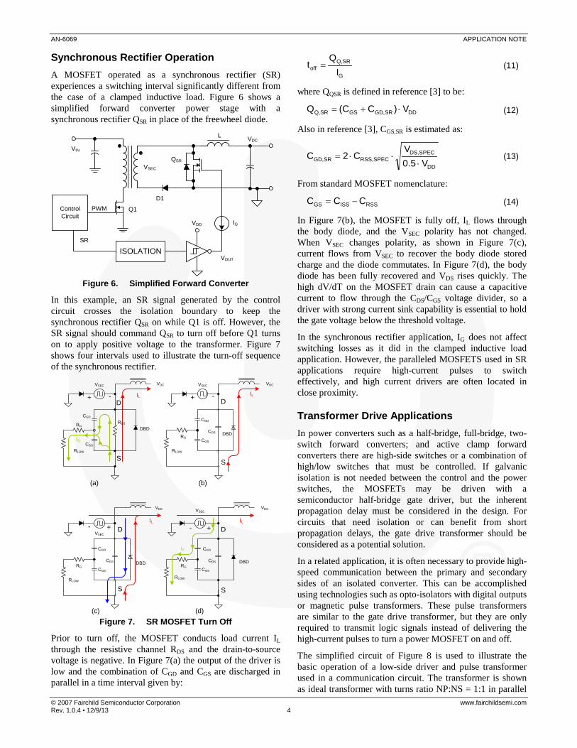
Synchronous Rectifier Operation A MOSFET operated as a synchronous rectifier (SR) experiences a switching interval significantly different from the case of a clamped inductive load. Figure 6 shows a simplified forward converter power stage with a synchronous rectifier QSR in place of the freewheel diode.
VIN
VDC
IGVDD
ControlCircuit
ISOLATION
QSR
L
Q1
VSEC
PWM
SR
D1
VOUT
Figure 6. Simplified Forward Converter
In this example, an SR signal generated by the control circuit crosses the isolation boundary to keep the synchronous rectifier QSR on while Q1 is off. However, the SR signal should command QSR to turn off before Q1 turns on to apply positive voltage to the transformer. Figure 7 shows four intervals used to illustrate the turn-off sequence of the synchronous rectifier.
(a) (b)
(c) (d)
CGD
CGS
IL
RG
VSEC VDC
DBD
RLOW
-+
IG
RDS
S
D
CGD
CGS
CDS
IL
RG
VDC
DBD
RLOW
VSEC
-+ D
S
VDC
CGD
CGS
CDS
IL
RG
VDC
DBD
RLOW
CGD
CGS
CDS
IL
RGDBD
RLOW
IG
VSEC
- +
VSEC
- +D D
S S
Figure 7. SR MOSFET Turn Off
Prior to turn off, the MOSFET conducts load current IL through the resistive channel RDS and the drain-to-source voltage is negative. In Figure 7(a) the output of the driver is low and the combination of CGD and CGS are discharged in parallel in a time interval given by:
G
SR,Qoff I
Qt = (11)
where QQSR is defined in reference [3] to be:
DDSR,GDGSSR,Q V)CC(Q ⋅+= (12)
Also in reference [3], CGS,SR is estimated as:
DD
SPEC,DSSPEC,RSSSR,GD V5.0
VC2C
⋅⋅⋅= (13)
From standard MOSFET nomenclature:
RSSISSGS CCC −= (14)
In Figure 7(b), the MOSFET is fully off, IL flows through the body diode, and the VSEC polarity has not changed. When VSEC changes polarity, as shown in Figure 7(c), current flows from VSEC to recover the body diode stored charge and the diode commutates. In Figure 7(d), the body diode has been fully recovered and VDS rises quickly. The high dV/dT on the MOSFET drain can cause a capacitive current to flow through the CDS/CGS voltage divider, so a driver with strong current sink capability is essential to hold the gate voltage below the threshold voltage.
In the synchronous rectifier application, IG does not affect switching losses as it did in the clamped inductive load application. However, the paralleled MOSFETS used in SR applications require high-current pulses to switch effectively, and high current drivers are often located in close proximity.
Transformer Drive Applications In power converters such as a half-bridge, full-bridge, two-switch forward converters; and active clamp forward converters there are high-side switches or a combination of high/low switches that must be controlled. If galvanic isolation is not needed between the control and the power switches, the MOSFETs may be driven with a semiconductor half-bridge gate driver, but the inherent propagation delay must be considered in the design. For circuits that need isolation or can benefit from short propagation delays, the gate drive transformer should be considered as a potential solution.
In a related application, it is often necessary to provide high-speed communication between the primary and secondary sides of an isolated converter. This can be accomplished using technologies such as opto-isolators with digital outputs or magnetic pulse transformers. These pulse transformers are similar to the gate drive transformer, but they are only required to transmit logic signals instead of delivering the high-current pulses to turn a power MOSFET on and off.
The simplified circuit of Figure 8 is used to illustrate the basic operation of a low-side driver and pulse transformer used in a communication circuit. The transformer is shown as ideal transformer with turns ratio NP:NS = 1:1 in parallel

AN-6069 APPLICATION NOTE
© 2007 Fairchild Semiconductor Corporation www.fairchildsemi.com Rev. 1.0.4 • 12/9/13 5
with magnetizing inductance LMAG. In both cases, the DC blocking capacitor CC is large enough so that its voltage is approximately constant.
R
CC
VDDT1
NP:NS
VS
-
+
VP
+
-
+
-
VOUT
IR
IDR
IMAG
IN LMAG
Figure 8. Simplified Pulse Transformer Circuit
In Figure 9, the circuit is modified so that the resistor is replaced by the gate-to-source terminal of a MOSFET located on the high side of a bridge circuit.
CC
VDD T1NP:NS
VS
-
+VP
+
-
+
-
VOUT
IGIDR
IMAG
IN LMAG
+Bulk
Figure 9. Simplified Gate Drive Transformer Circuit
0(a) shows the operational waveforms for the pulse transformer circuit, while 0(b) shows operation in a gate drive application.
VOUT
IDR
IR
IMAG
VS
VP
tSW
tON
VOUT
IDR
IG
IMAG
VS
VP
tSW
tON
u se Gate e
(a) (b)
Figure 10. (a) Pulse Transformer Waveforms and (b) Gate Drive Transformer Waveforms
The output of the driver swings from 0V to VDD producing a DC component equal to VDD x duty cycle. If this voltage is
applied directly to the primary winding of T1, the transformer would saturate and not be able to transmit useful information. To prevent this, coupling capacitor CC is inserted in series with the primary winding to block the DC voltage while passing the AC portion of the VOUT signal. Transformers designed for pulse and gate drive applications usually specify a voltage-time product the device can withstand without saturating the transformer.
In many cases, the same transformer could be used as either a pulse transformer operation or a gate drive transformer. In 0, the major difference between the two applications is in the current waveforms. With a constant drive voltage and magnetizing inductance, LMAG, the magnetizing current IMAG is the same in both circuits. In the pulse transformer waveforms shown in 0(a), the resistor current IR follows the secondary voltage VS, and the driver supplies a current that is the sum of these two components. In the MOSFET gate drive waveforms shown in 0(b), the gate current IG is positive pulses at turn on and negative pulses at turn off. As in the first example, the driver supplies a current that is the sum of these two components, but the waveform has a larger RMS value due to the high-current pulses.
It is important to examine the direction of current flow between driver and transformer for the examples of 0. When VOUT swings high as shown Figure 11(a), one might expect the driver to immediately source current. However, the magnetizing current is negative and, if the load current is not larger than the magnetizing current, the driver must sink current until IDR goes positive. The opposite situation exists in Figure 11(b), when VOUT goes from high to low and the driver must source current when expected to operate as a current sink. Figure 11(c) shows additional diodes providing a current path if the driver cannot sink current when VOUT is high or source current when VOUT is low, as found in drivers with a bipolar output stage.
VOUT
IDR
VOUT
IDR
Pulse Transformer Gate Transformer
(a)
VOUT
IDR
VOUT
IDR
Pulse Transformer Gate Transformer
(b)
AN-6069 APPLICATION NOTE
© 2007 Fairchild Semiconductor Corporation www.fairchildsemi.com Rev. 1.0.4 • 12/9/13 6
R
CC
VDD
T1NP:NS
VS
-
+
VP
+
-
+
-VOUT
IR
IDR
IMAG
IN LMAG
(c)
Figure 11. Current Flow and Diode Clamp Circuit for Transformer Driver
If the transformer is designed with low leakage inductance, the propagation delays through the transformer can be less than 50ns. The GT03 series of transformers from ICE Components[4] is an example of devices with leakage inductance of a few hundred nanoHenries. This is achieved by using tightly coupled windings on a small ferrite core.
In the previous transformer examples, the positive and negative peaks vary with duty cycle, while the secondary voltage VS swings around zero volts. In a pulse transformer application, the pulses might feed circuits that cannot accept the negative-going pulses. The circuit in Figure 12 incorporates a clamp circuit consisting of a second coupling capacitor CCS and a diode that restores the DC level of the secondary voltage.
CCRS
VDD T1NP:NS
VS
-
+
CCS
VSIG
+
-
Figure 12. Pulse Transformer with DC Restore Circuit
Series resistor RS serves to damp the initial transient at startup when CCS is initially uncharged, and is often a discrete resistor in addition to the internal driver impedance. From classical RLC circuit theory, a value of RS for critical damping is approximately:
CC
MAGS C
L2R ⋅= (15)
where LMAG is the magnetizing inductance of the transformer.
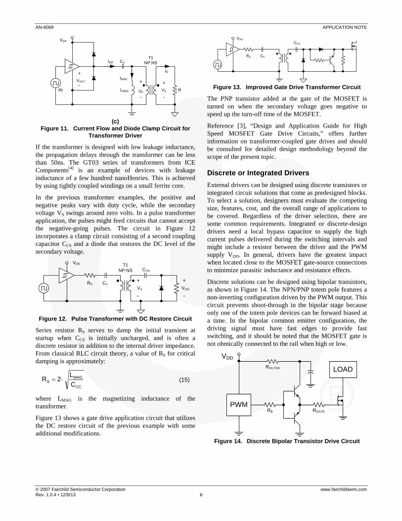
Figure 13 shows a gate drive application circuit that utilizes the DC restore circuit of the previous example with some additional modifications.
VDD
CC
CCS
RS
Figure 13. Improved Gate Drive Transformer Circuit
The PNP transistor added at the gate of the MOSFET is turned on when the secondary voltage goes negative to speed up the turn-off time of the MOSFET.
Reference [3], “Design and Application Guide for High Speed MOSFET Gate Drive Circuits,” offers further information on transformer-coupled gate drives and should be consulted for detailed design methodology beyond the scope of the present topic.
Discrete or Integrated Drivers External drivers can be designed using discrete transistors or integrated circuit solutions that come as predesigned blocks. To select a solution, designers must evaluate the competing size, features, cost, and the overall range of applications to be covered. Regardless of the driver selection, there are some common requirements. Integrated or discrete-design drivers need a local bypass capacitor to supply the high current pulses delivered during the switching intervals and might include a resistor between the driver and the PWM supply VDD. In general, drivers have the greatest impact when located close to the MOSFET gate-source connections to minimize parasitic inductance and resistance effects.
Discrete solutions can be designed using bipolar transistors, as shown in Figure 14. The NPN/PNP totem pole features a non-inverting configuration driven by the PWM output. This circuit prevents shoot-through in the bipolar stage because only one of the totem pole devices can be forward biased at a time. In the bipolar common emitter configuration, the driving signal must have fast edges to provide fast switching, and it should be noted that the MOSFET gate is not ohmically connected to the rail when high or low.
RGATERB
PWM
VDD
RFILTER LOAD
Figure 14. Discrete Bipolar Transistor Drive Circuit

AN-6069 APPLICATION NOTE
© 2007 Fairchild Semiconductor Corporation www.fairchildsemi.com Rev. 1.0.4 • 12/9/13 7
The PMOS/NMOS version shown in Figure 15 has a natural inversion and would require an inverter to follow the PWM signal polarity. This circuit offers rail-to-rail operation, but shoot-through is a problem that must be considered in design because both devices can conduct when the common gate node voltage is in the middle part of the VDD range.
RGATE
PWM
VDD
RFILTER
PossibleInversion
LOAD
Figure 15. Discrete PMOS/NMOS Drive Circuit
Using the discrete driver approach leads to a higher component count that requires more PCB board space and more assembly and test time. The higher component count can lead to more procurement costs and reliability concerns. If the input signal comes from a logic circuit or a low-voltage PWM, the discrete driver requires additional circuitry to translate from logic levels to power drive levels.
Integrated circuit drivers offer significant benefits in addition to large pulse current capability. New integrated dual drivers in 3x3mm packages and single drivers in 2x2mm packages include a thermal pad for heat removal. These devices require less board space than discrete solutions, while offering enhanced thermal performance, so they are well-suited for the most dense power designs. Features integrated into the device, such as an enable function and UVLO, create ease of use and reduce component-level design. It has been common practice to offer drivers with TTL-compatible input thresholds that can accept inputs ranging from logic-level signals up to the VDD range of the device. Drivers utilizing CMOS input thresholds (2/3 VDD = high, 1/3VDD = low) can help alleviate noise issues or set more accurate timing delays at the input of the driver.
Driver Datasheet Current Ratings Driver datasheet current ratings and test conditions can lead to confusion. Many consider the gate driver to be a near ideal voltage source that can instantly deliver current as determined by the circuit series resistance. This is not necessarily true. Usually, the current available from a driver is limited by the internal circuit design, regardless of the semiconductor technology used. This self-limiting nature should not be confused with self-protecting; if a driver output is shorted high or low, the device is likely to fail.
Common methods used for driver datasheet current ratings:
• Peak current available from device, usually at initial turn on at maximum VDD
• Current available with the output clamped at a specific voltage, often around VDD/2
• Current available with low value resistance to rails (perhaps 0.5Ω, even short circuit)
• Current measured with a current probe Integrated MOSFET drivers are commonly available in one of three technologies: primarily MOSFET, bipolar, or a combination of the two, often referred to as “compound” devices. The MOSFET and bipolar versions are similar to the discrete solutions previously mentioned, while the compound design combines features from both technologies.
For low-side drivers built with a MOS output state (PMOS high side and NMOS low side, similar to the discrete circuit illustrated in Figure 15), the datasheet current rating is generally specified as the peak current available from the part, often specified with VDD near the maximum rating of the part. Figure 16 shows the output current and voltage for a 4A driver using test methods detailed in the section “Evaluating Drivers on the Bench” below. This testing shows that the internal circuitry limits the peak output current to a value near the rated 4A with no external resistor.
VOUT at 2V/div
IOUT at 1A/div
IN at 5V/div
Time = 200ns/div
Figure 16. PMOS/NMOS Driver VOUT and IOUT The PMOS/NMOS drivers usually specify the driver output resistance when it is sinking or sourcing a specified current, such as 100mA. It is interesting to note that the MOS-type driver does not attain the RO,high or RO,low resistance values immediately when the device begins switching. For example, 4A drivers commonly specify a value for RO,high or RO,low from 1 – 2Ω. If the devices reached this low resistance value instantaneously, the peak currents would be more than 7A with VDD = 15V.
In compound devices, bipolar and MOSFET devices are combined in a parallel configuration, such as the one shown in Figure 17, where the power output devices are shaded. The bipolar transistors are able to deliver high sink and source current, while the output voltage swings through the middle of the output range. The PMOS and NMOS operate in parallel with the bipolar devices to pull the output voltage to the positive or negative rail as required.

AN-6069 APPLICATION NOTE
© 2007 Fairchild Semiconductor Corporation www.fairchildsemi.com Rev. 1.0.4 • 12/9/13 8
Inputstage
VDD
VOUT
Figure 17. Compound Driver Output Stage
For compound drivers, the output current is often specified with the output voltage at a specified voltage, such as VDD/2, to highlight the current that is available during the Miller plateau region of the VGS waveform. In tests performed using the methods described in section “Evaluating Drivers on the Bench” below, the peak output current is generally higher than the current specified at VDD/2. Figure 18 shows the sink current capability of a 4A compound driver (FAN3224C) to be 4.76A, while the output is at 6.1V after reaching a peak just under 6A. A compound driver rated at 4A might deliver a higher peak current than a comparably rated PMOS/NMOS driver. This type of information is practically impossible to obtain from the driver datasheets, so specific test methods are required.
IOUT at 2A/div
VOUT at 5V/div
INPUT at 10V/div
Time = 200ns/div
Figure 18. Compound Driver Current Sink Waveform
Evaluating Drivers on the Bench Real-world driver comparisons are difficult to perform in the lab because the fast signal ramp rates cause complex interactions between the inductive and capacitive circuit components. These fast edge rates can introduce overshoots and undershoots of several volts. Some examples to help quantify this effect in power circuits can be found in reference [5]. Although the parasitic inductance varies
according to specific circuit layout and ground structure, reference [6] gives an approximate value of 10nH/inch (4nH/cm) for microstrip on FR-4 with the trace exposed to air on one side. This provides an estimate that can be used with the circuit capacitance to calculate a damping resistor when needed.
It is difficult to compare competing devices using only datasheets, which offer information produced using different test conditions. Competing technologies used in integrated circuit solutions further complicate device comparison. In the following paragraphs, several circuits that can be used to test and compare drivers on the bench are presented.
Figure 19 shows a circuit that can be used to test the pulsed current source capability of a driver by clamping VOUT to a level equal to VDSCH + VDZEN when the output is high. To minimize power dissipation, the input is driven with a 200ns positive-going pulse (for non-inverting driver) with a 2% duty cycle. In this circuit, the positive-going voltage across RCS is used to monitor the current sourced out of the driver. To change the value of the output clamping voltage, the voltage rating of DZEN must be changed.
VDD
RCS
VPULSE
DZEN
DSCH
VCS
+
-
CBYP
VOUT
Figure 19. Current Source Test Circuit with
Clamped VOUT
Figure 20 shows a circuit used to test the pulsed current sink capability of a driver with the output voltage clamped at a level VADJ-VDSCH. Here, the input is driven with a 200ns negative-going pulse (for a non-inverting driver) with a 2% duty cycle. In this circuit, the negative-going voltage across RCS is used to monitor the current that the driver is sinking.
VDD
RCS
VPULSE
C1
DSCH
VADJ
VCS
+
-
CBYP
VOUT
Figure 20. Current Sink Test Circuit with Clamped VOUT

AN-6069 APPLICATION NOTE
© 2007 Fairchild Semiconductor Corporation www.fairchildsemi.com Rev. 1.0.4 • 12/9/13 9
In both these circuits, there is a voltage transient that may last for 50-100ns as the current increases to the limits of the driver. A compact layout using surface mount components keeps the loop area small to minimize parasitic inductance.
The two previous circuits require a unique surface mount layout. It is possible to evaluate driver current capability by connecting a relatively large capacitive load on the output of a driver with the simple circuit shown in Figure 21.
CLOAD
VDD=12V
IPRB
VOUT
CBYP
Figure 21. "Large" Load Test Circuit
For a starting point, CLOAD is chosen to be 100 times larger than the load used for rise and fall time measurements and the input is driven with a 1kHz square wave. On typical datasheets, 2A drivers are specified with 1nF load for the rise and fall time specifications, so CLOAD would be selected to be 0.1µF. This relatively large load prevents the output from changing rapidly, allowing the driver output current to reach its internal limiting value. A current probe, IPRB, can be used to monitor the output current along with the output voltage VOUT on an oscilloscope. This enables plotting the output current available at the corresponding output voltage. Bench comparisons have shown that the current measurement obtained using this method agrees closely with that obtained using the clamp circuits in Figure 19 and Figure 20. In addition, the slower current rise and fall times allow the current measurements to be made comfortably within the bandwidth limits of a current probe.
Figure 22 shows the waveforms obtained using the test circuit shown in Figure 21 to evaluate a 2A sink / 1.5A source driver (FAN3227C) with a compound output stage. When the driver input, VIN, goes high, there is a transient glitch on the VOUT trace as the output current quickly increases to 3A through the inductance of the current probe loop. After approximately 70ns, the current has reached its peak value and the voltage spike across the parasitic inductances vanishes. With VOUT = 6V, the output current is measured as 1.5A (source current).
VOUT at 5V/div
INPUT at 10V/div
IOUT at 2A/div
Time = 200ns/div
Figure 22. Compound Driver Current Source Waveforms
Figure 22 shows the leading spike across the inductance introduced by the wire loop inserted in the circuit to enable use of a current probe. If the wire loop is removed and the 0.1µF surface mount capacitor is installed in a layout with minimal parasitic inductance, the waveforms shown in Figure 23 are obtained. In short intervals where the voltage waveform is approximately linear, the basic relation is:
⋅=dT
dVCI OUTLOAD (16)
can be applied to provide an estimate of the current.
VOUT at 2V/div
INPUT at 10V/div
Time = 200ns/div
Figure 23. Compound Driver Current Estimation
The oscillogram in Figure 23 allows calculation of current during the cursor interval as:
A8.2ns6.40V131.1µF1.0I =
⋅= (17)
providing close agreement with the peak value seen in the IOUT trace in Figure 22. A similar calculation around VOUT = 6V provides a current estimation of 1.5A, nearly identical to the result obtained with direct current measurement using a current probe. The close agreement between the current measurement techniques using the large load helps develop confidence in the results obtained.

AN-6069 APPLICATION NOTE
© 2007 Fairchild Semiconductor Corporation www.fairchildsemi.com Rev. 1.0.4 • 12/9/13 10
Conclusion Low-side drivers are used to drive power MOSFETs in applications including clamped inductive load switching, synchronous rectifier circuits, and pulse/gate transformer drive circuits. The relationship of gate drive current to the MOSFET switching and transition intervals has been detailed during the prominent MOSFET switching intervals. Potential driver solutions; including discrete components, integrated PMOS/NMOS, and compound drivers, were examined. Some of the non-ideal characteristics of the various driver circuits were highlighted.
There is not a simple unified method to characterize the output current sink and source capability of the many types of drivers available. The test circuits presented in this note can be used to investigate the VOUT vs. IOUT capability of discrete and integrated circuit drivers, enabling evaluation and comparison of drivers for a range of applications.
References [1] 2006 Fairchild Power Seminar Topic, “Understanding Modern Power MOSFETs,” available on the fairchildsemi.com website at the link:
http://www.fairchildsemi.com/powerseminar/pdf/understanding_modern_power_mOSFETs.pdf [2] Oh, K. S., “MOSFET Basics”, July, 2000, available as AN9010 from the fairchildsemi.com website. [3] Balogh, L. “Design and Application Guide for High Speed MOSFET Gate Drive Circuits,” Power Supply Design Seminar SEM-1400, Topic 2,
Texas Instruments Literature No. SLUP169. [4] ICE Components Gate Drive Transformer Datasheet “GT03.pdf” dated 10/06, available from www.icecomponents.com. [5] 2006 Fairchild Power Seminar Topic, “Practical Power Application Issues for High Power Systems,” available on the fairchildsemi.com website at the
link: http://www.fairchildsemi.com/powerseminar/pdf/practical_power_high_power_systems.pdf [6] Johnson, H. Dr, “High-Speed Digital Design On-Line Newsletter,” Vol. 3 Issue 8, www.sigcon.com/Pubs/news/3_8.htm
AuthorMark Dennis was born in Troy, NC, and received the Bachelor of Engineering degree from Duke University in 1983. After graduation he has worked in industries encompassing power electronics applications such as offline and DC to DC power supply design for telecom and computer systems, high voltage supplies for electrostatic precipitators, and online UPS systems. For over eight years Mark has been working in the semiconductor industry and he is employed by Fairchild Semiconductor as a Staff Engineer working in High Power Systems.

AN-6069 APPLICATION NOTE
© 2007 Fairchild Semiconductor Corporation www.fairchildsemi.com Rev. 1.0.4 • 12/9/13 11
Related Parts
Type Part Number
Gate Drive(1) (Sink/Src)
Input Threshold Logic Package
Single 1A FAN3111C +1.1A / -0.9A CMOS Single Channel of Dual-Input/Single-Output SOT23-5, MLP6
Single 1A FAN3111E +1.1A / -0.9A External(2) Single Non-Inverting Channel with External Reference SOT23-5, MLP6
Single 2A FAN3100C +2.5A / -1.8A CMOS Single Channel of Two-Input/One-Output SOT23-5, MLP6
Single 2A FAN3100T +2.5A / -1.8A TTL Single Channel of Two-Input/One-Output SOT23-5, MLP6
Dual 2A FAN3216T +2.4A / -1.6A TTL Dual Inverting Channels SOIC8
Dual 2A FAN3217T +2.4A / -1.6A TTL Dual Non-Inverting Channels SOIC8
Dual 2A FAN3226C +2.4A / -1.6A CMOS Dual Inverting Channels + Dual Enable SOIC8, MLP8
Dual 2A FAN3226T +2.4A / -1.6A TTL Dual Inverting Channels + Dual Enable SOIC8, MLP8
Dual 2A FAN3227C +2.4A / -1.6A CMOS Dual Non-Inverting Channels + Dual Enable SOIC8, MLP8
Dual 2A FAN3227T +2.4A / -1.6A TTL Dual Non-Inverting Channels + Dual Enable SOIC8, MLP8
Dual 2A FAN3228C +2.4A / -1.6A CMOS Dual Channels of Two-Input/One-Output, Pin Config.1 SOIC8, MLP8
Dual 2A FAN3228T +2.4A / -1.6A TTL Dual Channels of Two-Input/One-Output, Pin Config.1 SOIC8, MLP8
Dual 2A FAN3229C +2.4A / -1.6A CMOS Dual Channels of Two-Input/One-Output, Pin Config.2 SOIC8, MLP8
Dual 2A FAN3229T +2.4A / -1.6A TTL Dual Channels of Two-Input/One-Output, Pin Config.2 SOIC8, MLP8
Dual 2A FAN3268T +2.4A / -1.6A TTL 20V Non-Inverting Channel (NMOS) and Inverting Channel (PMOS) + Dual Enables SOIC8
Dual 2A FAN3278T +2.4A / -1.6A TTL 30V Non-Inverting Channel (NMOS) and Inverting Channel (PMOS) + Dual Enables SOIC8
Dual 4A FAN3213T +4.3A / -2.8A TTL Dual Inverting Channels SOIC8
Dual 4A FAN3214T +4.3A / -2.8A TTL Dual Non-Inverting Channels SOIC8
Dual 4A FAN3223C +4.3A / -2.8A CMOS Dual Inverting Channels + Dual Enable SOIC8, MLP8
Dual 4A FAN3223T +4.3A / -2.8A TTL Dual Inverting Channels + Dual Enable SOIC8, MLP8
Dual 4A FAN3224C +4.3A / -2.8A CMOS Dual Non-Inverting Channels + Dual Enable SOIC8, MLP8
Dual 4A FAN3224T +4.3A / -2.8A TTL Dual Non-Inverting Channels + Dual Enable SOIC8, MLP8
Dual 4A FAN3225C +4.3A / -2.8A CMOS Dual Channels of Two-Input/One-Output SOIC8, MLP8
Dual 4A FAN3225T +4.3A / -2.8A TTL Dual Channels of Two-Input/One-Output SOIC8, MLP8
Single 9A FAN3121C +9.7A / -7.1A CMOS Single Inverting Channel + Enable SOIC8, MLP8
Single 9A FAN3121T +9.7A / -7.1A TTL Single Inverting Channel + Enable SOIC8, MLP8
Single 9A FAN3122T +9.7A / -7.1A CMOS Single Non-Inverting Channel + Enable SOIC8, MLP8
Single 9A FAN3122C +9.7A / -7.1A TTL Single Non-Inverting Channel + Enable SOIC8, MLP8
Notes: 1. Typical currents with OUTx at 6V and VDD=12V. 2. Thresholds proportional to an externally supplied reference voltage. To review the datasheets for the above low-side gate drivers, visit Fairchild Semiconductor’s website at:
http://www.fairchildsemi.com/sitesearch/fsc.jsp?command=eq&attr1=AAAFamily&attr2=Low-Side+Drivers

AN-6069 APPLICATION NOTE
© 2007 Fairchild Semiconductor Corporation www.fairchildsemi.com Rev. 1.0.4 • 12/9/13 12
DISCLAIMER FAIRCHILD SEMICONDUCTOR RESERVES THE RIGHT TO MAKE CHANGES WITHOUT FURTHER NOTICE TO ANY PRODUCTS HEREIN TO IMPROVE RELIABILITY, FUNCTION, OR DESIGN. FAIRCHILD DOES NOT ASSUME ANY LIABILITY ARISING OUT OF THE APPLICATION OR USE OF ANY PRODUCT OR CIRCUIT DESCRIBED HEREIN; NEITHER DOES IT CONVEY ANY LICENSE UNDER ITS PATENT RIGHTS, NOR THE RIGHTS OF OTHERS. LIFE SUPPORT POLICY FAIRCHILD’S PRODUCTS ARE NOT AUTHORIZED FOR USE AS CRITICAL COMPONENTS IN LIFE SUPPORT DEVICES OR SYSTEMS WITHOUT THE EXPRESS WRITTEN APPROVAL OF THE PRESIDENT OF FAIRCHILD SEMICONDUCTOR CORPORATION. As used herein: 1. Life support devices or systems are devices or systems
which, (a) are intended for surgical implant into the body, or (b) support or sustain life, or (c) whose failure to perform when properly used in accordance with instructions for use provided in the labeling, can be reasonably expected to result in significant injury to the user.
2. A critical component is any component of a life support device or system whose failure to perform can be reasonably expected to cause the failure of the life support device or system, or to affect its safety or effectiveness.

www.onsemi.com1
ON Semiconductor and are trademarks of Semiconductor Components Industries, LLC dba ON Semiconductor or its subsidiaries in the United States and/or other countries.ON Semiconductor owns the rights to a number of patents, trademarks, copyrights, trade secrets, and other intellectual property. A listing of ON Semiconductor’s product/patentcoverage may be accessed at www.onsemi.com/site/pdf/Patent−Marking.pdf. ON Semiconductor reserves the right to make changes without further notice to any products herein.ON Semiconductor makes no warranty, representation or guarantee regarding the suitability of its products for any particular purpose, nor does ON Semiconductor assume any liabilityarising out of the application or use of any product or circuit, and specifically disclaims any and all liability, including without limitation special, consequential or incidental damages.Buyer is responsible for its products and applications using ON Semiconductor products, including compliance with all laws, regulations and safety requirements or standards,regardless of any support or applications information provided by ON Semiconductor. “Typical” parameters which may be provided in ON Semiconductor data sheets and/orspecifications can and do vary in different applications and actual performance may vary over time. All operating parameters, including “Typicals” must be validated for each customerapplication by customer’s technical experts. ON Semiconductor does not convey any license under its patent rights nor the rights of others. ON Semiconductor products are notdesigned, intended, or authorized for use as a critical component in life support systems or any FDA Class 3 medical devices or medical devices with a same or similar classificationin a foreign jurisdiction or any devices intended for implantation in the human body. Should Buyer purchase or use ON Semiconductor products for any such unintended or unauthorizedapplication, Buyer shall indemnify and hold ON Semiconductor and its officers, employees, subsidiaries, affiliates, and distributors harmless against all claims, costs, damages, andexpenses, and reasonable attorney fees arising out of, directly or indirectly, any claim of personal injury or death associated with such unintended or unauthorized use, even if suchclaim alleges that ON Semiconductor was negligent regarding the design or manufacture of the part. ON Semiconductor is an Equal Opportunity/Affirmative Action Employer. Thisliterature is subject to all applicable copyright laws and is not for resale in any manner.
PUBLICATION ORDERING INFORMATIONN. American Technical Support: 800−282−9855 Toll FreeUSA/Canada
Europe, Middle East and Africa Technical Support:Phone: 421 33 790 2910
Japan Customer Focus CenterPhone: 81−3−5817−1050
www.onsemi.com
LITERATURE FULFILLMENT:Literature Distribution Center for ON Semiconductor19521 E. 32nd Pkwy, Aurora, Colorado 80011 USAPhone: 303−675−2175 or 800−344−3860 Toll Free USA/CanadaFax: 303−675−2176 or 800−344−3867 Toll Free USA/CanadaEmail: [email protected]
ON Semiconductor Website: www.onsemi.com
Order Literature: http://www.onsemi.com/orderlit
For additional information, please contact your localSales Representative
© Semiconductor Components Industries, LLC