dspace.jaist.ac.jp · biphenyl (cbp) having different ionization energy to fabri- ... high-purity...
TRANSCRIPT

Japan Advanced Institute of Science and Technology
JAIST Repositoryhttps://dspace.jaist.ac.jp/
Title
Enhancement of hole injection and
electroluminescence characteristics by a rubbing-
induced lying orientation of alpha-sexithiophene
Author(s) Matsushima, Toshinori; Murata, Hideyuki
CitationJournal of Applied Physics, 112(2): 024503-1-
024503-9
Issue Date 2012-07-17
Type Journal Article
Text version publisher
URL http://hdl.handle.net/10119/10868
Rights
Copyright 2012 American Institute of Physics.
This article may be downloaded for personal use
only. Any other use requires prior permission of
the author and the American Institute of Physics.
The following article appeared in Toshinori
Matsushima and Hideyuki Murata, Journal of
Applied Physics, 112(2), 024503 (2012) and may be
found at http://dx.doi.org/10.1063/1.4735402
Description

Enhancement of hole injection and electroluminescence characteristics bya rubbing-induced lying orientation of alpha-sexithiopheneToshinori Matsushima and Hideyuki Murata Citation: J. Appl. Phys. 112, 024503 (2012); doi: 10.1063/1.4735402 View online: http://dx.doi.org/10.1063/1.4735402 View Table of Contents: http://jap.aip.org/resource/1/JAPIAU/v112/i2 Published by the American Institute of Physics. Related ArticlesNitrogen-polar core-shell GaN light-emitting diodes grown by selective area metalorganic vapor phase epitaxy Appl. Phys. Lett. 101, 032103 (2012) Nanostructure Ag dots for improving thermal stability of Ag reflector for GaN-based light-emitting diodes Appl. Phys. Lett. 101, 021115 (2012) Electrical measurement of internal quantum efficiency and extraction efficiency of III-N light-emitting diodes Appl. Phys. Lett. 101, 021113 (2012) Efficient organic light-emitting diodes through up-conversion from triplet to singlet excited states of exciplexes APL: Org. Electron. Photonics 5, 149 (2012) Space charge induced electroluminescence spectra shift in organic light-emitting diodes J. Appl. Phys. 112, 014513 (2012) Additional information on J. Appl. Phys.Journal Homepage: http://jap.aip.org/ Journal Information: http://jap.aip.org/about/about_the_journal Top downloads: http://jap.aip.org/features/most_downloaded Information for Authors: http://jap.aip.org/authors

Enhancement of hole injection and electroluminescence characteristicsby a rubbing-induced lying orientation of alpha-sexithiophene
Toshinori Matsushima and Hideyuki Murataa)
School of Materials Science, Japan Advanced Institute of Science and Technology, 1-1 Asahidai, Nomi,Ishikawa 923-1292, Japan
(Received 5 January 2012; accepted 9 June 2012; published online 17 July 2012)
The authors find that rubbing a film of alpha-sexithiophene (a-6T) with a nylon cloth induces a change
from standing to lying orientations in a film surface region. While current densities of hole-only devices
based on 4,40,400-tris(N-3-methylphenyl-N-phenyl-amino)triphenylamine (m-MTDATA) are independent
of the rubbing number of a-6T, current densities of hole-only devices based on N-N0-diphenyl-N-N0-bis(1-naphthyl)-1,10-biphenyl-4,40-diamine (a-NPD) and 4,40-bis(carbazol-9-yl)-2,20-biphenyl (CBP)
markedly increase (�42 times at 1 V for the a-NPD devices and�236 times at 1 V for the CBP devices)
as the rubbing number of a-6T is increased. The increase in current density is ascribed to enhanced hole
injection through a �5.28 eV energy level of lying a-6T domains instead of a �4.95 eV energy level of
standing a-6T domains and improved overlaps between an electronic cloud of indium tin oxide, porbitals of lying a-6T molecules, and p orbitals of molecules of a-NPD and CBP at heterojunction
interfaces. The rubbing of a-6T is also demonstrated to reduce drive voltages (by �40% at 10 mA/cm2)
and increase power conversion efficiency (by �26% at 10 mA/cm2) of organic light-emitting
diodes. Finally, half lifetimes are significantly enhanced (4.3 times) at a current density of 50 mA/cm2.VC 2012 American Institute of Physics. [http://dx.doi.org/10.1063/1.4735402]
I. INTRODUCTION
Charge injection and transport processes in organic elec-
tronic devices such as organic light-emitting diodes (OLEDs)
are key factors affecting their current density-voltage
characteristics.1,2 To reduce driving voltage of OLEDs,
high-charge-mobility organic materials have been used3,4
and device structures having minimized heterojunction
energy barriers have been designed.5,6 Also, doping an or-
ganic layer with a strong electron donor or acceptor material
is effective due to an increase in electrical conductivity and
formation of a quasi-Ohmic contact at organic/electrode
interfaces.7,8 The other way to reduce the power consump-
tion is suggested to be control of an orientation of organic
molecules. It is well known that organic films and crystals
based on a face-to-face stacked orientation of molecules
relative to each other (for example, a herringbone configura-
tion) exhibit favorable charge transport due to an overlap of
p orbitals.9,10 This stacked orientation concept has been fre-
quently used in a research area of organic thin-film transis-
tors to increase charge mobility.11,12 If a molecular
orientation can be controlled in a multilayer OLED, charge
injection efficiency at a heterojunction interface as well as
bulk charge mobility are enhanced, leading to a reduction in
power consumption. For examples of previous reports
regarding orientations of organic small molecules, Era et al.used homoepitaxial growth of p-sexiphenyl (6P) on a rubbed
surface to obtain polarized electroluminescence (EL) from
an oriented 6P film.13 Yanagi and Okamoto constructed
OLEDs by depositing 6P and additional layers on a KCl
(001) surface and transferring the multilayer structure to an
indium tin oxide (ITO)-coated substrate.14 A lying orienta-
tion of 6P, deposited at a lower temperature, resulted in a
lower drive voltage than a standing orientation. Yokoyama
et al. demonstrated that planar-shaped long organic mole-
cules in vacuum-deposited amorphous films were oriented
parallel to a substrate plane.15 However, the most of vacuum-
deposited organic molecules are generally random and it is
still underdeveloped to control an orientation of organic small
molecules in solid-state films for device applications,
whereas there are many techniques used to align long-chain
polymers along a certain direction.16–18
Recently, we demonstrated that rubbing a film of alpha-
sexithiophene (a-6T) with a nylon cloth induced a change
from standing to lying orientations in a film surface region.19
The lying orientation of a-6T increased current densities of
hole-only devices by 42 times at 1 V due to enhanced hole
injection from a-6T to N-N0-diphenyl-N-N0-bis(1-naphthyl)-
1,10-biphenyl-4,40-diamine (a-NPD), offering an alternative
possibility of manufacturing sophisticated organic electronic
devices with low power consumption. The aim of this report
is to clarify a mechanism of the enhanced hole injection by
combining the previous data (Ref. 19) with our recent data.
In this study, we choose three kinds of organic material:
4,40,400-tris(N-3-methylphenyl-N-phenyl-amino)triphenylamine
(m-MTDATA), a-NPD, and 4,40-bis(carbazol-9-yl)-2,20-biphenyl (CBP) having different ionization energy to fabri-
cate hole-only devices and investigate how the rubbing
number of a-6T and hole injection barriers at the interfaces
of a-6T/m-MTDTA, a-6T/a-NPD, and a-6T/CBP affect cur-
rent density-voltage characteristics of the hole-only devices.
In addition to the discussion of the hole injection mecha-
nism, we demonstrate that the lying orientation of a-6T
caused by the rubbing results in a reduction in voltage anda)Electronic mail: [email protected].
0021-8979/2012/112(2)/024503/9/$30.00 VC 2012 American Institute of Physics112, 024503-1
JOURNAL OF APPLIED PHYSICS 112, 024503 (2012)

increases in power conversion efficiency and operational
lifetime of OLEDs based on stacked layers of a-NPD and
tris(8-hydroxyquinoline)aluminum (Alq3).
II. EXPERIMETAL
The chemical structures of organic molecules used in
this study are shown in Fig. 1(a). High-purity source materi-
als of a-NPD (Nippon Steel Chemical), CBP (Nippon Steel
Chemical), Alq3 (Nippon Steel Chemical), MoO3 (Mitsuwa
Chemical), LiF (Nacalai Tesque), and Al (Nilaco) were used
as received and source materials of a-6T (Aldrich) and m-
MTDATA (Luminescence Technology) were purified twice
using a temperature-gradient vacuum train sublimation tech-
nique prior to use. Fused silica substrates and glass substrates
coated with a 150 nm ITO layer having sheet resistance of
10 X/sq (SLR grade, Sanyo Vacuum Industries) were cleaned
using ultrasonication in acetone, followed by ultrasonication
in detergent, pure water, and isopropanol. Then, the sub-
strates were placed in an ultraviolet (UV)-ozone treatment
chamber (PL21-200, SEN LIGHT) for 30 min.
Fifteen nm a-6T films were vacuum-deposited on the
cleaned fused silica substrates at a deposition rate of 0.1 nm/s
under a base pressure of 10�5 Pa using a vacuum deposition
system (E-200, ALS technology). The resulting film thick-
ness and the deposition rate were controlled with a care-
fully calibrated quartz crystal microbalance. After the a-6T
deposition, the substrates were transferred to an adjacent
nitrogen-filled glove box (oxygen and water levels are lower
than 1 ppm) and the films were repeatedly rubbed 1, 5, 7, 10,
and 15 times using a 3.5 cm-diameter cylindrical vial wound
with a dust-free nylon cloth in a given direction. The rubbing
was conducted by hand, so that the rubbing condition was not
controlled precisely, but the transfer speed and the weight of
the vial on the films were roughly 25 cm/s and 500 g, respec-
tively. The films were characterized using an UV/visible
(UV-vis) absorption spectrometer (V670, JASCO) and an
atomic force microscope (AFM) (VN-8000, KEYENCE) in air.
The structures of the hole-only devices and the OLEDs
were glass substrate/ITO anode (150 nm)/rubbed a-6T/a-NPD
(100 nm)/MoO3 (10 nm)/Al cathode (100 nm) and glass
substrate/ITO anode (150 nm)/rubbed a-6T/a-NPD (90 nm)/
Alq3 (70 nm)/LiF (0.5 nm)/Al cathode (100 nm), respectively
[see the device structures shown in Figs. 1(b) and 1(c)]. After
the a-6T layer was vacuum-deposited on the cleaned ITO
layer and then rubbed using the similar way mentioned
before, the additional layers were vacuum-deposited on top
of the rubbed layer to complete the devices. The hole-only
devices and the OLEDs without a-6T and rubbing were also
fabricated for comparison. The devices were encapsulated
using a glass cap and an UV curing epoxy resin together
with a dessicant sheet, which absorbs both oxygen and water.
All fabrication processes were conducted without exposing
the samples to air. The device area was 2.25 mm2, which
was defined as the overlapped area of the ITO layer and the
Al layer. The deposition rates were set at 0.1 nm/s (a-6T, m-
MTDATA, a-NPD, CBP, and Alq3), 0.05 nm/s (MoO3),
0.01 nm/s (LiF), and 0.5 nm/s (Al). The current density-volt-
age-external quantum efficiency characteristics of the devi-
ces were measured using a computer-controlled sourcemeter
(2400, Keithley) and an integrating sphere installed with a
calibrated silicon photodiode. The luminance and the power
conversion efficiency of the OLEDs were measured using a
computer-controlled luminance meter (BM-9, TOPCON).
The EL spectra of the OLEDs were taken using a photonic
multi-channel analyzer (C7473, Hamamatsu). To evaluate
the operational stability, the changes in luminance and drive
voltage of the OLEDs were recorded with time using a life-
time measurement system (PEL-11OT, COMODO SOLU-
TIONS) when the devices were continuously operated at a
constant dc current density of 50 mA/cm2. All measurements
were conducted at room temperature.
III. RESULTS AND DISCUSSION
A. Change from standing to lying orientations of a-6Tby rubbing
First of all, we discuss the molecular orientation charac-
teristics of the as-deposited and rubbed a-6T films on the
fused silica substrates with conventional unpolarized UV-vis
absorption spectra, which are measured under light incidence
normal (0�) and oblique (45�) to the substrate [Figs. 2(a) and
2(b)]. The absorption in this wavelength range originates
from p-p* transition of a-6T having an electronic transition
moment along its long molecular axis.20 There are a strong
absorption peak at �360 nm and weak vibronic side peaks at
400–600 nm in the as-deposited film. The �360 nm peak
decreases and the 400–600 nm peaks relatively increase in
absorbance after the rubbing. The �360 nm peak completely
disappears in the films rubbed 10 and 15 times. Egelhaaf
et al. reported that a thin a-6T film had a sharp blue-shifted
absorption peak originating from aggregates of a-6T mole-
cules on a substrate surface.21 An increase in a-6T thickness
reduced the sharp absorption peak and increased the vibronic
side absorption peaks in intensity because of reduced molec-
ular order for thicker films. Since the spectral change
induced by the rubbing resembles the result of the Egelhaaf’s
report, the �360 nm peak and the 400–600 nm peaks prob-
ably arise from aggregated and unaggregated a-6T mole-
cules, respectively. One well-known example of the sharpFIG. 1. (a) Chemical structures of organic molecules used in this study and
schematic structures of (b) hole-only devices and (c) OLEDs.
024503-2 T. Matsushima and H. Murata J. Appl. Phys. 112, 024503 (2012)

blue-shifted absorption peak is formation of H-aggregates.
The disappearance of the �360 nm peak in the 10 and 15
times rubbed films means decomposition of aggregated mol-
ecules into unaggregated molecules and/or removal of large
aggregated molecules with the nylon cloth.
The areas of the unpolarized absorption spectra shown
in Figs. 2(a) and 2(b) are calculated in the wavelength range
from 300 to 600 nm and plotted versus the rubbing number
in Fig. 2(c). The oblique-incidence measurement is expected
to increase the areas by H2 compared with the normal-
incidence measurement because of an increase in path length
of light. However, for the as-deposited film, the area
obtained with the oblique incidence is about two times larger
than that obtained with the normal incidence, indicating that
the standing orientation of a-6T is dominant for the as-
deposited film because standing molecules can absorb the
oblique-incidence light more strongly than the normal-
incidence light. It has been reported that the majority of
vacuum-deposited a-6T molecules stands on a hydrophilic
substrate,20 which agrees with the result obtained here.
The areas gradually decrease as the rubbing number is
increased because of a decrease in film thickness by the rub-
bing. When the films are rubbed 10 and 15 times, the areas
obtained with the oblique incidence become smaller than
those obtained with the normal incidence, suggesting that the
standing orientation is predominantly changed into the lying
orientation. The similar orientation rearrangement has been
reported in a rubbed 6P film.22
The polarized absorption spectra of the as-deposited and
rubbed films were measured under the normal light incidence
when an electric field vector of incident light is polarized
parallel and perpendicular to the rubbing direction. The data
of the absorption dichroic ratios estimated from the polarized
spectra are shown in the inset of Fig. 2(c). The absorption
dichroic ratio is unity for the as-deposited film, indicating
random a-6T molecules in the film plane while the standing
a-6T orientation is dominant in the thickness direction. The
dichroic ratios gradually increase from 1 to 13 as the rubbing
number is increased from 0 to 15. Thus, lying a-6T mole-
cules caused by the rubbing are aligned along the rubbing
direction to some extent.
The surface morphology of the as-deposited and rubbed
a-6T films are measured using the AFM. The as-deposited
film has a relatively smooth surface with small grains [Fig.
3(a)]. After rubbing the films, one can observe an uneven
striped texture along the rubbing direction and an increase in
surface roughness [Figs. 3(b) and 3(c)], meaning that the
films are not rubbed uniformly with the nylon cloth and the
lying orientation occurs under the partially rubbed surface
regions. The number of the stripes changes and the surface
roughness reduces at the larger rubbing number [Figs.
3(d)–3(f)]. Thus, we assume that the lying orientation
regions gradually spread on the film surface as the rubbing
number is increased.
To investigate a possibility of a rubbing-induced change
in electronic state of a-6T, we previously measured photo-
electron yield spectra of the as-deposited and rubbed a-6T
films using an AC-2 photoelectron yield spectrometer (Riken
Keiki).19 The ionization energy estimated from our photo-
electron yield spectra was unchanged between the as-
deposited and rubbed films because the rubbed films were
too thin (a few nanometer) to detect photoelectrons pre-
cisely. Therefore, we prepare thick 50 nm a-6T films on the
bare substrate surface and on the 15 times rubbed a-6T sur-
face for the ionization energy measurement. We can confirm
from UV-vis absorption spectroscopy that the 50 nm a-6T
films on the bare substrate surface and the 15 times rubbed
surface mainly include standing and lying a-6T molecules,
respectively (this data will be published elsewhere). The ion-
ization energy is calculated to be 4.95 6 0.02 eV for standing
a-6T molecules and 5.28 6 0.02 eV for lying a-6T molecules
from the changes in slope in the photoelectron yield spectra
shown in Fig. 4(a), demonstrating that the ionization energy
is dependent upon the molecular orientation. It has been
reported that a change from standing to lying orientations of
a-6T increases its ionization energy,23 which agrees with our
ionization energy results. Thus, two kinds of energy level
are probably formed in the rubbed films: one lies on
�4.95 eV (originating from standing a-6T molecules) and
the other lies on �5.28 eV (originating from lying a-6T
molecules).
Based on the results discussed before, we propose the
cross sectional structures of the as-deposited and rubbed
films as illustrated in Fig. 4(b). Since the films are partially
rubbed using the nylon cloth (Fig. 3), four kinds of domain
with different electronic states are probably formed in the
rubbed films (see Fig. 4(b)):
FIG. 2. Unpolarized absorption spectra of as-deposited and rubbed a-6T
films measured with (a) normal and (b) oblique light incidence and (c) plots
of spectral areas obtained with normal and oblique light incidence versus
rubbing number. Inset shows change in absorption dichroic ratio as function
of rubbing number when polarized absorption spectra are measured with
normal light incidence.
024503-3 T. Matsushima and H. Murata J. Appl. Phys. 112, 024503 (2012)

(A) Standing a-6T domain: In the domains, surfaces of
which are not in contact with the rubbing cloth, standing
a-6T molecules are kept intact. Therefore, the standing
a-6T domains have the �4.95 eV energy level.
(B) Standing/lying a-6T domain: In the domains, surfaces
of which are partially shaved with the rubbing cloth,
the domains of this sort have a bilayer orientation
structure, where a thin layer of lying a-6T molecules
with the �5.28 eV energy level resides on an intact
layer of standing a-6T molecules with the �4.95 eV
energy level.
(C) Lying a-6T domain: In the domains, surfaces of which
are mostly shaved with the rubbing cloth, a thin layer of
lying a-6T molecules with the �5.28 eV energy level is
only left on the substrate.
(D) Bare substrate domain: In the domains, all a-6T mole-
cules are removed from the substrate with the rubbing
cloth, resulting in appearance of a bare substrate surface.
The as-deposited film only contains the homogeneous
domains of standing a-6T molecules having the �4.95 eV
energy level [(A) standing a-6T domain]. On the other hand,
the four domains of (A) standing a-6T, (B) standing/lying
a-6T, (C) lying a-6T, and (D) bare substrate coexist in the
rubbed films. As the rubbing number is increased, the
domains (B), (C), and (D) gradually increase in the films,
affecting the current density-voltage characteristics of the
hole-only devices and the OLEDs presented later because
FIG. 3. AFM images and their cross section
profiles of (a) as-deposited, (b) 1 time, (c) 5
times, (d) 7 times, (e) 10 times, and (f) 15
times rubbed a-6T films.
FIG. 4. (a) Photoelectron yield spectra (electrons per incident photons) of
50 nm a-6T films on bare substrate surface and 15 times rubbed a-6T surface
and (b) illustrations of proposed molecular orientations for as-deposited and
rubbed a-6T films.
024503-4 T. Matsushima and H. Murata J. Appl. Phys. 112, 024503 (2012)
the �5.28 eV energy level is more favorable for hole injec-
tion than the �4.95 eV energy level.
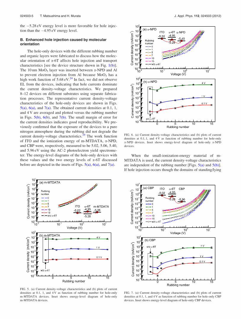
B. Enhanced hole injection caused by molecularorientation
The hole-only devices with the different rubbing number
and organic layers were fabricated to discuss how the molec-
ular orientation of a-6T affects hole injection and transport
characteristics [see the device structure shown in Fig. 1(b)].
The 10 nm MoO3 layer was inserted between a-NPD and Al
to prevent electron injection from Al because MoO3 has a
high work function of 5.68 eV.24 In fact, we did not observe
EL from the devices, indicating that hole currents dominate
the current density-voltage characteristics. We prepared
8–12 devices on different substrates using separate fabrica-
tion processes. The representative current density-voltage
characteristics of the hole-only devices are shown in Figs.
5(a), 6(a), and 7(a). The obtained current densities at 0.1, 1,
and 4 V are averaged and plotted versus the rubbing number
in Figs. 5(b), 6(b), and 7(b). The small margin of error for
the current densities indicates good reproducibility. We pre-
viously confirmed that the exposure of the devices to a pure
nitrogen atmosphere during the rubbing did not degrade the
current density-voltage characteristics.19 The work function
of ITO and the ionization energy of m-MTDATA, a-NPD,
and CBP were, respectively, measured to be 5.02, 5.06, 5.40,
and 5.96 eV using the AC-2 photoelectron yield spectrome-
ter. The energy-level diagrams of the hole-only devices with
these values and the two energy levels of a-6T discussed
before are depicted in the insets of Figs. 5(a), 6(a), and 7(a).
When the small-ionization-energy material of m-
MTDATA is used, the current density-voltage characteristics
are independent of the rubbing number [Figs. 5(a) and 5(b)].
If hole injection occurs though the domains of standing/lying
FIG. 5. (a) Current density-voltage characteristics and (b) plots of current
densities at 0.1, 1, and 4 V as function of rubbing number for hole-only
m-MTDATA devices. Inset shows energy-level diagram of hole-only
m-MTDATA devices.
FIG. 6. (a) Current density-voltage characteristics and (b) plots of current
densities at 0.1, 1, and 4 V as function of rubbing number for hole-only
a-NPD devices. Inset shows energy-level diagram of hole-only a-NPD
devices.
FIG. 7. (a) Current density-voltage characteristics and (b) plots of current
densities at 0.1, 1, and 4 V as function of rubbing number for hole-only CBP
devices. Inset shows energy-level diagram of hole-only CBP devices.
024503-5 T. Matsushima and H. Murata J. Appl. Phys. 112, 024503 (2012)

a-6T (B) and lying a-6T (C), the current densities of the
rubbed devices are likely to decrease, but the obtained result
is different. Since the Fermi level of ITO (�5.02 eV) and the
hole transport levels of standing a-6T (�4.95 eV) and m-
MTDATA (�5.06 eV) are close to each other, holes are prob-
ably injected from ITO to m-MTDATA through the �4.95 eV
hole transport level of the narrowly residual standing a-6T
domains (A) [the inset of Fig. 5(a)] or injected directly from the
bare ITO domains (D), resulting in the rubbing-independent
current density-voltage characteristics.
For the a�NPD devices, the current densities of the
unrubbed device are lower than those of the device without
a-6T perhaps because of an increased hole-injection barrier
at the a-6T/a-NPD interface [the inset of Fig. 6(a)], but we
find that the current densities increase (�42 times at 1 V) as
the rubbing number is increased from 0 to 15 [Figs. 6(a) and
6(b)]. Since the current densities of the 15 times rubbed de-
vice are higher than those of the device without a-6T, the
reduction in a-6T thickness caused by the rubbing is not the
major factor for the increased current densities. It has been
reported that a hole mobility of a-6T is measured to be
10�4�10�2 cm2/V s using a thin-film transistor structure,25
which is presumably higher than that of a-NPD (10�4–10�3
cm2/V s) measured using a time-of-flight technique,26
suggesting that the bulk hole transport (the hole mobility) of
a-6T therefore does not limit the current density-voltage
characteristics.
The �5.28 eV hole transport level of the lying a-6T
domains (C) is more favorable for hole injection than the
�4.95 eV hole transport level of the standing a-6T domains
(A) because the �5.28 eV hole transport level is intermediate
between the Fermi level of ITO (�5.02 eV) and the hole
transport level of a-NPD (�5.40 eV). We assume that the
hole transport sites in the a-6T layer shift from the standing
a-6T domains (A) to the lying a-6T domains (C) and the
area of the lying a-6T domains (C) increases gradually as the
rubbing number is increased, resulting in the increased cur-
rent densities. It is possible that improved overlaps between
an electronic cloud of ITO, p orbitals of lying a-6T mole-
cules, and p orbitals of a-NPD molecules at the heterojunc-
tion interfaces increase the current densities as well. The
hole injection via the standing/lying a-6T domains (B) and
the bare ITO domains (D) are not probable for the rubbed a-
NPD devices because the hole injection of these sorts are en-
ergetically unfavorable.
For the CBP devices, we obtain the similar-shaped cur-
rent density-voltage and current density-rubbing number
characteristics to those of the a-NPD devices [Figs. 7(a) and
7(b)] because of the enhanced hole injection via the
�5.28 eV hole transport level of the lying a-6T domains (C)
and the improved overlaps between an electronic cloud of
ITO, p orbitals of lying a-6T molecules, and p orbitals of
CBP molecules at the heterojunction interfaces as discussed
before. Since there is the larger hole injection barrier at the
a-6T/CBP interface than that at the a-6T/a-NPD interface
for the unrubbed devices [the insets of Figs. 6(a), and 7(a)],
the current density-voltage characteristics of the unrubbed
CBP device must be limited by the hole injection process
from a-6T to CBP more strongly than that from a-6T to
a-NPD. Therefore, the current enhancement ratio of the CBP
devices (�236 at 1 V) would be much larger than that of the
a-NPD devices (�42 at 1 V). From these results, it is obvious
that the rubbing-induced lying orientation enhances charge
injection more effectively when a charge injection barrier
height is larger.
Alternatively, changes in orientation and crystallinity of
m-MTDATA, a-NPD, and CBP on the rubbed a-6T surface
are likely to occur and affect their hole mobility and hole
transport levels. Polarized absorption spectra of 10 nm films
of m-MTDATA, a-NPD,19 and CBP on the 15 times rubbed
a-6T surface were measured with the normal and oblique
light incidence to investigate their molecule orientation char-
acteristics. No absorption dichroisms were observed from all
films, indicating that these molecules are optically random
and the molecular orientations in the bulk layers do not occur
significantly on the rubbed surface.
We have previously demonstrated that current density-
voltage characteristics of the hole-only a-NPD devices are
independent of the rubbing number when ITO and Al are re-
versely wired as a cathode and an anode, respectively
(namely, a negative bias).19 The similar rubbing-independent
current density-voltage characteristics were obtained from
the negative biased hole-only devices of m-MTDATA and
CBP. The rubbing-independent current density-voltage char-
acteristics suggest that the hole mobility of m-MTDATA, a-
NPD, and CBP in these bulk layers are not changed signifi-
cantly. Thus, we can conclude that the enhanced hole injec-
tion by the formation of lying a-6T molecules and the
improved overlaps between an electronic cloud of ITO, porbitals of lying a-6T molecules, and p orbitals of molecules
of a-NPD and CBP are more essential for the increased cur-
rent densities than the increase in hole mobility. However,
we still cannot rule out the possibility of the changes in ori-
entation and crystallinity of m-MTDATA, a-NPD, and CBP
especially near the rubbed a-6T surface, which also affect
their hole transport levels and the current density-voltage
characteristics. There is room for further investigation on the
electronic states proposed here, so that we are now investi-
gating the electronic states of the stacked films in more detail
using ultraviolet photoelectron spectroscopy.
C. Improved performance of OLEDs with rubbed a-6Tlayers
We demonstrate the improvement of the OLED charac-
teristics using the rubbing-induced lying a-6T orientation.
The current density-voltage characteristics of the OLEDs are
shown in Figs. 8(a) (linear-linear scale) and 8(b) (logarith-
mic-linear scale). For easy to understand, the current den-
sities at 3, 5, and 8 V and the drive voltages at 1, 10, and 100
mA/cm2 are plotted together versus the rubbing number
[Fig. 8(c)]. We find that the current density-voltage charac-
teristics of the OLEDs [Fig. 8(a)] are changed in the manner
similar to those of the hole-only a-NPD devices [Fig. 6(a)],
indicating that the increase in current density of the OLEDs
is attributed to the enhanced hole injection by the formation
of lying a-6T molecules and the improved overlaps between
an electronic cloud of ITO, p orbitals of lying a-6T
024503-6 T. Matsushima and H. Murata J. Appl. Phys. 112, 024503 (2012)

molecules, and p orbitals of a-NPD molecules. It is likely
that the increase in surface roughness after the rubbing
(Fig. 3) results in an unexpected leakage current through the
OLEDs, but no significant leakage current is observed in a
low voltage region less than 2 V [Fig. 8(b)] probably because
of very good coverage of the rubbed surfaces with a-NPD
and Alq3. The current densities increase (�24 times at 5 V)
and the drive voltages decrease (by �40% at 10 mA/cm2) as
the rubbing number is increased from 0 to 15 [Fig. 8(c)].
Besides the hole injection from ITO to a-NPD through a-6T
and the hole transport in a-NPD, the processes of electron
transport in Alq3, electron injection from LiF/Al to Alq3, and
hole injection from a-NPD to Alq3 limit the current density-
voltage characteristics of the OLEDs to some extent. There-
fore, the current enhancement ratio of the OLEDs (�24 at 5 V)
would be smaller than that of the hole-only a-NPD devices
(�42 at 1 V). The drive voltages of the OLED without a-6T
are comparable to those of previously reported OLEDs based
on a-NPD and Alq3.27,28
We obtained similar EL spectra from every OLED, which
originate from electrically excited Alq3. The external quantum
efficiency is not changed significantly in comparison with the
drive voltages and the power conversion efficiency, but
slightly decrease (by �17% at 10 mA/cm2) at the larger rub-
bing number [Fig. 8(d)] because of an excess number of
injected holes in the Alq3 layer29 and/or exciton quenching by
accumulated holes at the a-NPD/Alq3 interface.30 On the other
hand, the power conversion efficiency increases by the rub-
bing (by �26% at 10 mA/cm2) [Fig. 8(d)] because the
decrease in voltage overcomes the decrease in external quan-
tum efficiency. The shapes and the peaks (525 6 5 nm) of the
EL spectra and the external quantum efficiency values (�1%)
are in good agreement with those of previously reported
OLEDs with an Alq3 emitter.31–33
The operational stability of the OLEDs is markedly de-
pendent upon the rubbing number. The luminance/initial
luminance-time and voltage-time characteristics of the
OLEDs are shown in Figs. 9(a) and 9(b). The initial lumi-
nance at the operation current density of 50 mA/cm2 is about
1500 cd/m2, which slightly depends on the rubbing number.
The half lifetimes and the voltage increase rates are, respec-
tively, defined as the time at which the luminance reduced to
half of their initial luminance and the slopes between the ini-
tial and last data points. The half lifetimes and the voltage
increase rates are plotted as a function of the rubbing number
in Fig. 9(c). The larger rubbing number makes it possible to
increase the half lifetimes and suppress the voltage increase
rates. The half lifetime of the 15 times rubbed OLED is 4.3
times longer than that of the unrubbed OLED. This is the
first demonstration of the enhanced OLED lifetimes by con-
trolling the molecular orientation.
Operating OLEDs under a higher voltage at a higher
temperature accelerates degradation of OLEDs, indicating
that device degradation rapidly proceeds under the high tem-
perature condition.34,35 The reduction in voltage caused by
the rubbing reduces a temperature increase inside the
OLEDs, perhaps suppressing generation of nonradiative
recombination centers and/or luminance quenchers in a car-
rier recombination zone. The photoluminescence (PL) spec-
tra from the Alq3 layers inside the fresh and operated
OLEDs were measured using the C7473 analyzer with an ex-
citation light wavelength of 425 nm, where a-NPD absorp-
tion is negligible, but weak Alq3 absorption is still present.
We obtained a reduction in PL intensity of Alq3 by �19% in
all OLEDs. Since the 425 nm light excites the whole Alq3
layer in the thickness direction, it is probable that PL inten-
sity in a thin carrier recombination zone near the a-NPD/
Alq3 interface is smaller than �19% obtained here. The
observed reduction in PL intensity is indicative of generation
of nonradiative recombination centers and/or luminance
quenchers in the Alq3 layers. Nevertheless, the detailed rea-
son of the enhanced lifetimes observed here has not yet been
understood to date, and so is under investigation now. Finally,
we would like to stress that our rubbing technique surely
FIG. 8. Current density-voltage characteristics [(a) linear-linear scale and
(b) logarithmic-linear scale] and plots of (c) current densities at 3, 5, and
8 V, (c) drive voltages at 1, 10, and 100 mA/cm2, (d) external quantum effi-
ciency at 1, 10, and 100 mA/cm2, and (d) power conversion efficiency at 1,
10, and 100 mA/cm2 as function of rubbing number for unrubbed and rubbed
OLEDs.
024503-7 T. Matsushima and H. Murata J. Appl. Phys. 112, 024503 (2012)

reduces the drive voltages and increases the power conversion
efficiency and the long-term stability of the OLEDs, which are
useful for practical applications.
IV. CONCLUSIONS
From results of absorption spectra and AFM images, we
find that rubbing an a-6T film with a nylon cloth induces a
change from standing to lying orientations in partially
rubbed film surface regions and the lying orientation regions
gradually spread through the film as rubbing number is
increased. In the rubbed a-6T film, two kinds of energy level
are probably formed: one lies on �4.95 eV (originating from
standing a-6T molecules) and the other lies on �5.28 eV
(originating from lying a-6T molecules). Hole-only devices
based on m-MTDATA, a-NPD, and CBP are fabricated on
the rubbed a-6T surfaces to investigate how the molecular
orientation of a-6T affects their current density-voltage
characteristics. While current densities of the m-MTDATA
devices are independent of the rubbing number, current den-
sities of the a-NPD and CBP devices markedly increase
(�42 times at 1 V for the a-NPD devices and �236 times at
1 V for the CBP devices) as the rubbing number of a-6T is
increased. The increased current densities are ascribed to
enhanced hole injection through the �5.28 eV energy level
of lying a-6T domains instead of the �4.95 eV energy level
of standing a-6T domains as well as and improved overlaps
between an electronic cloud of ITO, p orbitals of lying a-6T
molecules, and p orbitals of molecules of a-NPD and CBP
at heterojunction interfaces. We also find that the rubbing
of the a-6T layer reduces drive voltages (by �40% at
10 mA/cm2) and increases power conversion efficiency
(by �26% at 10 mA/cm2) and half lifetimes (4.3 times at
50 mA/cm2) of OLEDs because of the lying a-6T orientation.
A multilayer structure has been widely used in OLEDs and
organic solar cells (OSC) to improve their electron-to-photon
and photon-to-electron conversion efficiency. Although there
have been some reports regarding a naturally formed lying ori-
entation of organic molecules in a vacuum-deposited film,10,15
organic molecules in each layer of the standard multilayer devi-
ces are generally random. The lying molecular orientation dem-
onstrated here occurs only in the very thin a-6T layer, but the
improvement of the device performances caused by the lying
a-6T orientation is significant. If multilayer devices having
lying orientations of organic molecules in each layer can be
realized, excellent charge injection, transport, and collection
characteristics will be obtained. The lying orientation is also
useful to increase light out-coupling efficiency of OLEDs (Ref.
36) and light-harvesting efficiency of OSCs.37 We are currently
aiming at fabricating such lying orientation devices by homo-
and hetero-epitaxially growing several kinds of organic layer
on the rubbed surface.
ACKNOWLEDGMENTS
The authors are grateful to Grants-in-Aid for Scientific
Research of Japan (Grant Nos. 21760005, 20241034, and
20108012) for financial support. This research is supported
by the Japan Society for the Promotion of Science (JSPS)
through its “Funding Program for World-Leading Innovative
R&D on Science and Technology (FIRST Program).”
1I. D. Parker, J. Appl. Phys. 75, 1656 (1994).2A. P. Kulkarni, C. J. Tonzola, A. Babel, and S. A. Jenekhe, Chem. Mater.
16, 4556 (2004).3S.-J. Su, T. Chiba, T. Takeda, and J. Kido, Adv. Mater. 20, 2125 (2008).4Y. Sun, L. Duan, D. Zhang, J. Qiao, G. Dong, L. Wang, and Y. Qiu, Adv.
Funct. Mater. 21, 1881 (2011).5S. Tokito, K. Noda, and Y. Taga, J. Phys. D: Appl. Phys. 29, 2750 (1996).6T. Matsushima and C. Adachi, Appl. Phys. Lett. 92, 063306 (2008).7F. Huang, A. G. MacDiarmid, and B. R. Hsieh, Appl. Phys. Lett. 71, 2415
(1997).8J. Huang, M. Pfeiffer, A. Werner, J. Blochwitz, and K. Leo, Appl. Phys.
Lett. 80, 139 (2002).9V. C. Sundar, J. Zaumseil, V. Podzorov, E. Menard, R. L. Willett, T.
Someya, M. E. Gershenson, and J. A. Rogers, Science 303, 1644 (2004).10D. Yokoyama, Y. Setoguchi, A. Sakaguchi, M. Suzuki, and C. Adachi,
Adv. Funct. Mater. 20, 386 (2010).11D. J. Gundlach, T. N. Jackson, D. G. Schlom, and S. F. Nelson, Appl.
Phys. Lett. 74, 3302 (1999).12K. Takimiya, H. Ebata, K. Sakamoto, T. Izawa, T. Otsubo, and Y. Kunugi,
J. Am. Chem. Soc. 128, 12604 (2006).13M. Era, T. Tsutsui, and S. Saito, Appl. Phys. Lett. 67, 2436 (1995).
FIG. 9. (a) Luminance/initial luminance-time and (b) drive voltage-time
characteristics and (c) plots of half lifetimes and voltage increase rates for
unrubbed and rubbed OLEDs. Devices were operated under constant current
density of 50 mA/cm2.
024503-8 T. Matsushima and H. Murata J. Appl. Phys. 112, 024503 (2012)

14H. Yanagi and S. Okamoto, Appl. Phys. Lett. 71, 2563 (1997).15D. Yokoyama, A. Sakaguchi, M. Suzuki, and C. Adachi, Appl. Phys. Lett.
93, 173302 (2008).16J. C. Wittmann and P. Smith, Nature (London) 352, 414 (1991).17M. Grell and D. D. C. Bradley, Adv. Mater. 11, 895 (1999).18H. Sirringhaus, R. J. Wilson, R. H. Friend, M. Inbasekaran, W. Wu, E. P.
Woo, M. Grell, and D. D. C. Bradley, Appl. Phys. Lett. 77, 406 (2000).19T. Matsushima and H. Murata, Appl. Phys. Lett. 98, 253307 (2011).20D. Oelkrug, H.-J. Egelhaaf, and J. Haiber, Thin Solid Films 284–285, 267
(1996).21H.-J. Egelhaaf, P. Baiuerle, K. Rauer, V. Hoffmann, and D. Oelkrug,
Synth. Met. 61, 143 (1993).22N. Aoki, Y. Koshiba, and Y. Ueda, Jpn. J. Appl. Phys., Part 1 44, 4088 (2005).23S. Duhm, G. Heimel, I. Salzmann, H. Glowatzki, R. L. Johnson, A.
Vollmer, J. P. Rabe, and N. Koch, Nature Mater. 7, 326 (2008).24T. Matsushima, Y. Kinoshita, and H. Murata, Appl. Phys. Lett. 91, 253504
(2007).25X. Peng, G. Horowitz, D. Fichou, and F. Garnier, Appl. Phys. Lett. 57,
2013 (1990).26S. Naka, H. Okada, H. Onnagawa, Y. Yamaguchi, and T. Tsutsui, Synth.
Met. 111–112, 331 (2000).
27S. A. Van Slyke, C. H. Chen, and C. W. Tang, Appl. Phys. Lett. 69, 2160
(1996).28S.-F. Chen and C.-W. Wang, Appl. Phys. Lett. 85, 765 (2004).29T. Tsutsui, Mater. Res. Soc. Bull. 22, 39 (1997).30Y. Luo, H. Aziz, G. Xu, and Z. D. Popovic, Chem. Mater. 19, 2288
(2007).31T. Dobbertin, M. Kroeger, D. Heithecker, D. Schneider, D. Metzdorf, H.
Neuner, E. Becker, H.-H. Johannes, and W. Kowalsky, Appl. Phys. Lett.
82, 284 (2003).32P.-C. Kao, S.-Y. Chu, Z.-X. You, S. J. Liou, and C.-A. Chuang, Thin Solid
Films 498, 249 (2006).33K. Okumoto, H. Kanno, Y. Hamada, H. Takahashi, and K. Shibata, Appl.
Phys. Lett. 89, 013502 (2006).34I. D. Parker, Y. Cao, and C. Y. Yang, J. Appl. Phys. 85, 2441 (1999).35X. Zhou, J. He, L. S. Liao, M. Lu, X. M. Ding, X. Y. Hou, X. M. Zhang,
X. Q. He, and S. T. Lee, Adv. Mater. 12, 265 (2000).36J. Frischeisen, D. Yokoyama, A. Endo, C. Adachi, and W. Brutting, Org.
Electron. 12, 809 (2011).37V. Kazukauskas, V. Cyras, M. Pranaitis, C. Sentein, L. Rocha, P. Rai-
mond, I. Duyssens, I. Van Severen, T. Cleij, L. Lutsen, and D. Vander-
zande, Thin Solid Films 516, 8963 (2008).
024503-9 T. Matsushima and H. Murata J. Appl. Phys. 112, 024503 (2012)