autonomous audio headset switch with reduced
TRANSCRIPT

S1
VDD
EN
MICP SLEEVE
RING2
GNDA
Control
Logic
TS3A226AE
FET1 FET2
TIP
RING1MIC_BIAS
MIC
R1
C2Audio
Codec
FM Receiver
GNDB
TS3A226AEwww.ti.com SCDS346A –JUNE 2013–REVISED JULY 2013
Autonomous Audio Headset Switch with Reduced GND Switch RON and FM CapabilityCheck for Samples: TS3A226AE
1FEATURES DESCRIPTIONThe TS3A226AE is an audio headset switch that• Ground FET Switches (60mΩ typical)detects 3- or 4-pole 3.5mm accessories. For a 4-pole• Autonomous Detection of Headset Types: accessory with a microphone, the TS3A226AE also
3-Poles or 4-Poles (with MIC on SLEEVE or detects the MIC location and routes the microphoneRING2) and ground signals automatically. The ground signal
is routed through a pair of low-impedance ground• Microphone Line SwitchesFETs (60mΩ typical), resulting minimal impact on• Supports FM Signal Transmission Through the audio cross-talk performance. The autonomousGround FETs detection feature allows end users to plug in
• Reduction of Click/Pop Noise accessories with different audio pole configurationsinto the mobile device and have them operate• VDD Range: 2.6 V – 4.7 Vproperly with no added software control and• THD (Mic): 0.002% Typical complexity. The ground FETs of the device are
• Low Current Consumption: 6.5-µA Typical designed to allow FM signal pass-through, making itpossible to use the ground line of the headset as an• ±8kV Contract Discharge (IEC 61000-4-2) ESDFM antenna in mobile audio application.Performance on SLEEVE and RING2 PinsThe TS3A226AE is packaged within a 1.2mm ×
APPLICATIONS 1.2mm WCSP package, making it suitable for use inmobile application.• Mobile Phones / Tablet PCs
• Notebook/Ultrabook Computers
Figure 1. Typical Application Diagram
ORDERING INFORMATION
For the most current package and ordering information, see the Package Option Addendum at the end of thisdocument, or see the TI web site at www.ti.com
1
Please be aware that an important notice concerning availability, standard warranty, and use in critical applications ofTexas Instruments semiconductor products and disclaimers thereto appears at the end of this data sheet.
PRODUCTION DATA information is current as of publication date. Copyright © 2013, Texas Instruments IncorporatedProducts conform to specifications per the terms of the TexasInstruments standard warranty. Production processing does notnecessarily include testing of all parameters.

C
B
A
1 2 3
A1 A2 A3
B1 B2 B3
C1 C2 C3C
B
A
3 2 1
A3 A2 A1
B3 B2 B1
C3 C2 C1
TS3A226AESCDS346A –JUNE 2013–REVISED JULY 2013 www.ti.com
These devices have limited built-in ESD protection. The leads should be shorted together or the device placed in conductive foamduring storage or handling to prevent electrostatic damage to the MOS gates.
PACKAGE; YFF-WCSP
Top View/Footprint Bump ViewDie Size: 1.2mm ×1.2mm
Bump Size: 0.25mmBump Pitch: 0.4mm
TS3A226AE Pin Mapping (Top View)3 2 1
C GND TIP ENB SLEEVE GNDA MICpA RING2 GNDB VDD
PIN FUNCTIONSPIN
DESCRIPTIONNUMB NAME TYPEERA1 VDD Supply Power supply for the chip.A2 GNDB Ground FET2 ground reference.A3 RING2 I/O Connected to the RING2 segment of the jack. The pin will be routed automatically by TS3A226AE to
either MICp or GNDB depending on the type of accessory.B1 MICp I/O Microphone signal connection to codec. Microphone bias should be fed into this pin.B2 GNDA Ground FET1 ground reference.B3 SLEEVE I/O Connected to the SLEEVE segment of the jack. The pin will be routed automatically by TS3A226AE to
either MICp or GNDA depending on the type of accessory.C1 EN Input A rising edge triggers the detection sequence. This pin can be connected to the headset jack to allow
automatic pull-up to supply after headset insertion.C2 TIP I/O Connected to the TIP segment of the headphone jack.C3 GND Ground Chip ground reference.
2 Submit Documentation Feedback Copyright © 2013, Texas Instruments Incorporated
Product Folder Links :TS3A226AE

MICp
SLEEVE
RING2
SW1
SW2
TS3A226AEwww.ti.com SCDS346A –JUNE 2013–REVISED JULY 2013
S1 MUX DETAIL
Figure 2. S1 Mux Detail
FUNCTIONAL TABLES: INTERNAL SWITCHES
EN Accessory Type Accessory Configuration SW1 SW2 FET1 FET20 N/A — High Z High Z High Z High Z
TIP = Audio Left1 TRS 3-pole Headphone or Speaker Ring = Audio Right On On On On
Sleeve = GroundTIP = Audio Left
Ring1 = Audio Right1 TRRS 4-pole Headphone On High Z High Z OnRing2 = GroundSleeve = Microphone
TIP = Audio LeftRing1 = Audio Right1 TRRS 4-pole Headphone High Z On On High ZRing2 = Microphone
Sleeve = Ground1 N/A — On On On On
ABSOLUTE MAXIMUM RATINGSover operating free-air temperature range (unless otherwise noted) (1)
VALUE UNITVoltage range on VDD (2) –0.3 to 5 V
VI Voltage range on EN, MICP, RING2, SLEEVE, TIP (2) –0.3 to VDD+0.5 VTA Operating ambient temperature range (3) –40 to 85 °CTJ (MAX) Maximum operating junction temperature 125 °CTstg Storage temperature range –65 to 150 °C
Charge device model (JESD 22 C101) 500 VESD rating Human body model(JESD 22 A114) 2 kV
Contact discharge on RING2, SLEEVE, TIP (IEC 61000-4-2) 8 kV
(1) Stresses beyond those listed under absolute maximum ratings may cause permanent damage to the device. These are stress ratingsonly, and functional operation of the device at these or any other conditions beyond those indicated under recommended operatingconditions is not implied. Exposure to absolute–maximum–rated conditions for extended periods may affect device reliability.
(2) All voltage values are with respect to network ground terminal.(3) In applications where high power dissipation and/or poor package thermal resistance is present, the maximum ambient temperature may
have to be derated. Maximum ambient temperature [TA(max)] is dependent on the maximum operating junction temperature [TJ(max)], themaximum power dissipation of the device in the application [PD(max)], and the junction-to-ambient thermal resistance of the part/packagein the application (θJA), as given by the following equation: TA(max) = TJ(max) – (θJA × PD(max))
Copyright © 2013, Texas Instruments Incorporated Submit Documentation Feedback 3
Product Folder Links :TS3A226AE

TS3A226AESCDS346A –JUNE 2013–REVISED JULY 2013 www.ti.com
RECOMMENDED OPERATING CONDITIONSover operating free-air temperature range (unless otherwise noted)
MIN MAX UNITVDD Supply voltage range 2.6 4.5 VVIO Input/Output voltage range (EN, MICP, RING2, SLEEVE, TIP) 0 VDD VVIO(TIP) Input/Output voltage range for TIP -2.0 VDD V
VDD = 2.6 V 1.16 VDD
VIH Input Logic High for EN VDD = 3.3 V 1.24 VDD VVDD = 4.5 V 1.48 VDD
VDD = 2.6 V 0 0.19VIL Input Logic Low for EN VDD = 3.3 V 0 0.3 V
VDD = 4.5 V 0 0.5TA Operating temperature range –40 85 °C
KEY ELECTRICAL CHARACTERISTICSUnless otherwise noted the specification applies over the VDD range and operating junction temperature –40°C ≤ TA ≤ 70°C.Typical values are for VDD = 3.3V and TJ = 25°C.
PARAMETER TEST CONDITIONS MIN TYP MAX UNITVDD Input Voltage Range 2.6 3.3 4.5 V
VDD = 4.5 V, VMICp = 1.8 V to VDD, EN=L orIDD Quiescent Current 6.5 14 µAEN=H (after detection)SWITCH RESISTANCERF1 FET1 On Resistance 60 85
VDD = 2.6 V, VGND = 0 V, IGND = 10 mA mΩRF2 FET2 On Resistance 60 85RSW1 SW1 On Resistance 8.5 10.5VDD = 2.6 V, VSLEEVE/RING2 = 0 V to 2.6 V, ΩIMIC = ±10 mARSW2 SW2 On Resistance 8.5 10.5SWITCH LEAKAGE CURRENTIOFF-0.1 FET1 and FET2 off leakage 1IOFF-10 SW1, SW2 off leakage VIN = 0 V to 2.6 V, VOUT = 0 V, VDD = 4.5 V 1 µAION-10 SW1, SW2 on leakage 1SWITCH DYNAMIC CHARACTERISTICSBWF1 FET1 Bandwidth 160 200
V = 60 mVPP, Ibias = 10 mA MHzBWF2 FET2 Bandwidth 160 200PSR217 V = 200 mVPP, f = 217 Hz –110 dB
Power Supply Rejection,PSR1k V = 200 mVPP, f = 1 kHz –100 dBRL = 50 ΩPSR20k V = 200 mVPP, f = 20 kHz –85 dBISOS1 SLEEVE or RING2 to MICP Isolation V = 200 mVPP, f = 20 kHz, RL = 50 Ω –80 dB
V = 200 mVPP, f = 20 kHz, RL = 50 ΩSEPS1 SLEEVE to RING2 Separation –80 dB(see Figure 5)THD10 V = 10 mVPP, f = 20-20 kHz, RS = 600 Ω 0.01%
Total Harmonic DistortionTHD200 V = 200 mVPP, f = 20-20 kHz, RS = 600 Ω 0.002%TIMING CHARACTERISTICStdect Total detection time From EN=H to S1 switch(es) closing 180 ms
4 Submit Documentation Feedback Copyright © 2013, Texas Instruments Incorporated
Product Folder Links :TS3A226AE
0.0001
0.001
0.01
0.1
1
20 200 2000 20000
TH
D (
%)
Frequency (Hz)
10mVPP
200mVPP
C002
10mVPP
200mVPP
0.0001
0.001
0.01
0.1
1
20 200 2000 20000
TH
D (
%)
Frequency (Hz)
10mVPP
200mVPP
C003
10mVPP
200mVPP
0.044
0.046
0.048
0.05
0.052
0.054
0.056
0.058
0.06
0.062
2.6 2.7 2.8 2.9 3 3.1 3.2 3.3 3.4 3.5 3.6 3.7 3.8 3.9 4 4.1 4.2 4.3 4.4 4.5
RO
N (
VDD (V)
FET1
FET2
C001
±15.00
±13.00
±11.00
±9.00
±7.00
±5.00
±3.00
±1.00
1.00
3.00
100k 1M 10M 100M 1000M
dB
(S
(2,1
)
Frequency (Hz)
FET2
FET1
C004
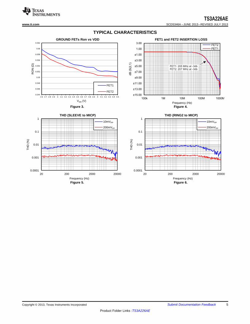
FET1: 205 MHz at -3dbFET2: 207 MHz at -3db
TS3A226AEwww.ti.com SCDS346A –JUNE 2013–REVISED JULY 2013
TYPICAL CHARACTERISTICSGROUND FETs Ron vs VDD FET1 and FET2 INSERTION LOSS
Figure 3. Figure 4.
THD (SLEEVE to MICP) THD (RING2 to MICP)
Figure 5. Figure 6.
Copyright © 2013, Texas Instruments Incorporated Submit Documentation Feedback 5
Product Folder Links :TS3A226AE

TS3A226AESCDS346A –JUNE 2013–REVISED JULY 2013 www.ti.com
REVISION HISTORY
Changes from Original (June 2013) to Revision A Page
• Removed Machine Model ESD specification. ....................................................................................................................... 3• Added EN=L or EN=H (after detection) to IDD TEST CONDITIONS. ................................................................................... 4• Added typical values to RSW1 and RSW2. ............................................................................................................................... 4• Added tdect PARAMETER to KEY ELECTRICAL CHARACTERISTICS table. ..................................................................... 4
6 Submit Documentation Feedback Copyright © 2013, Texas Instruments Incorporated
Product Folder Links :TS3A226AE

PACKAGE OPTION ADDENDUM
www.ti.com 10-Dec-2020
Addendum-Page 1
PACKAGING INFORMATION
Orderable Device Status(1)
Package Type PackageDrawing
Pins PackageQty
Eco Plan(2)
Lead finish/Ball material
(6)
MSL Peak Temp(3)
Op Temp (°C) Device Marking(4/5)
Samples
TS3A226AEYFFR ACTIVE DSBGA YFF 9 3000 RoHS & Green SNAGCU Level-1-260C-UNLIM -40 to 85 YP226AE
(1) The marketing status values are defined as follows:ACTIVE: Product device recommended for new designs.LIFEBUY: TI has announced that the device will be discontinued, and a lifetime-buy period is in effect.NRND: Not recommended for new designs. Device is in production to support existing customers, but TI does not recommend using this part in a new design.PREVIEW: Device has been announced but is not in production. Samples may or may not be available.OBSOLETE: TI has discontinued the production of the device.
(2) RoHS: TI defines "RoHS" to mean semiconductor products that are compliant with the current EU RoHS requirements for all 10 RoHS substances, including the requirement that RoHS substancedo not exceed 0.1% by weight in homogeneous materials. Where designed to be soldered at high temperatures, "RoHS" products are suitable for use in specified lead-free processes. TI mayreference these types of products as "Pb-Free".RoHS Exempt: TI defines "RoHS Exempt" to mean products that contain lead but are compliant with EU RoHS pursuant to a specific EU RoHS exemption.Green: TI defines "Green" to mean the content of Chlorine (Cl) and Bromine (Br) based flame retardants meet JS709B low halogen requirements of <=1000ppm threshold. Antimony trioxide basedflame retardants must also meet the <=1000ppm threshold requirement.
(3) MSL, Peak Temp. - The Moisture Sensitivity Level rating according to the JEDEC industry standard classifications, and peak solder temperature.
(4) There may be additional marking, which relates to the logo, the lot trace code information, or the environmental category on the device.
(5) Multiple Device Markings will be inside parentheses. Only one Device Marking contained in parentheses and separated by a "~" will appear on a device. If a line is indented then it is a continuationof the previous line and the two combined represent the entire Device Marking for that device.
(6) Lead finish/Ball material - Orderable Devices may have multiple material finish options. Finish options are separated by a vertical ruled line. Lead finish/Ball material values may wrap to twolines if the finish value exceeds the maximum column width.
Important Information and Disclaimer:The information provided on this page represents TI's knowledge and belief as of the date that it is provided. TI bases its knowledge and belief on informationprovided by third parties, and makes no representation or warranty as to the accuracy of such information. Efforts are underway to better integrate information from third parties. TI has taken andcontinues to take reasonable steps to provide representative and accurate information but may not have conducted destructive testing or chemical analysis on incoming materials and chemicals.TI and TI suppliers consider certain information to be proprietary, and thus CAS numbers and other limited information may not be available for release.
In no event shall TI's liability arising out of such information exceed the total purchase price of the TI part(s) at issue in this document sold by TI to Customer on an annual basis.

TAPE AND REEL INFORMATION
*All dimensions are nominal
Device PackageType
PackageDrawing
Pins SPQ ReelDiameter
(mm)
ReelWidth
W1 (mm)
A0(mm)
B0(mm)
K0(mm)
P1(mm)
W(mm)
Pin1Quadrant
TS3A226AEYFFR DSBGA YFF 9 3000 180.0 8.4 1.46 1.36 0.7 4.0 8.0 Q1
PACKAGE MATERIALS INFORMATION
www.ti.com 17-Jun-2015
Pack Materials-Page 1

*All dimensions are nominal
Device Package Type Package Drawing Pins SPQ Length (mm) Width (mm) Height (mm)
TS3A226AEYFFR DSBGA YFF 9 3000 182.0 182.0 20.0
PACKAGE MATERIALS INFORMATION
www.ti.com 17-Jun-2015
Pack Materials-Page 2
www.ti.com
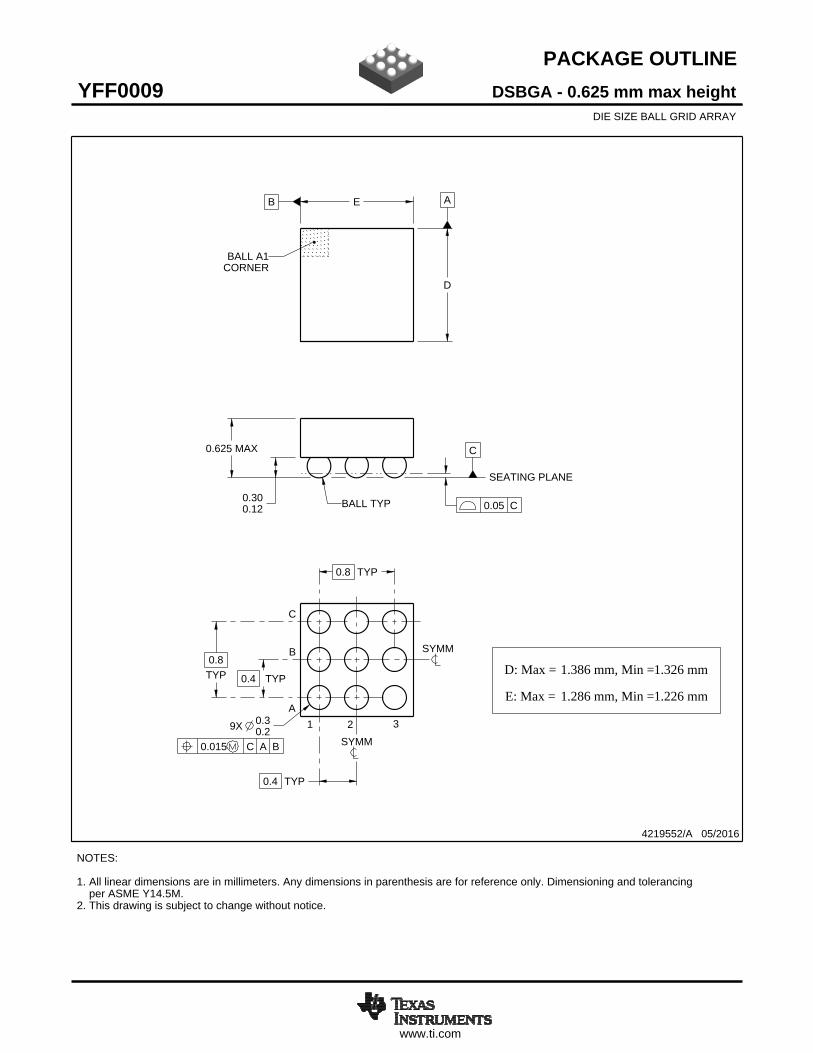
PACKAGE OUTLINE
C0.625 MAX
0.300.12
0.8TYP
0.8 TYP
0.4 TYP
0.4 TYP
9X 0.30.2
B E A
D
DSBGA - 0.625 mm max heightYFF0009DIE SIZE BALL GRID ARRAY
4219552/A 05/2016
NOTES: 1. All linear dimensions are in millimeters. Any dimensions in parenthesis are for reference only. Dimensioning and tolerancing per ASME Y14.5M.2. This drawing is subject to change without notice.
BALL A1CORNER
SEATING PLANE
BALL TYP 0.05 C
B
1 2 3
0.015 C A B
SYMM
SYMM
A
C
SCALE 10.000
D: Max =
E: Max =
1.386 mm, Min =
1.286 mm, Min =
1.326 mm
1.226 mm

www.ti.com
EXAMPLE BOARD LAYOUT
9X ( 0.23)
(0.4) TYP
(0.4) TYP
( 0.23)METAL
0.05 MAX
SOLDER MASKOPENING
METAL UNDERSOLDER MASK
( 0.23)SOLDER MASKOPENING
0.05 MIN
DSBGA - 0.625 mm max heightYFF0009DIE SIZE BALL GRID ARRAY
4219552/A 05/2016
NOTES: (continued) 3. Final dimensions may vary due to manufacturing tolerance considerations and also routing constraints. For more information, see Texas Instruments literature number SNVA009 (www.ti.com/lit/snva009).
SYMM
SYMM
LAND PATTERN EXAMPLESCALE:30X
C
1 2 3A
B
NON-SOLDER MASKDEFINED
(PREFERRED)
SOLDER MASK DETAILSNOT TO SCALE
SOLDER MASKDEFINED

www.ti.com
EXAMPLE STENCIL DESIGN
(0.4) TYP
(0.4) TYP
9X ( 0.25) (R0.05) TYP
METALTYP
DSBGA - 0.625 mm max heightYFF0009DIE SIZE BALL GRID ARRAY
4219552/A 05/2016
NOTES: (continued) 4. Laser cutting apertures with trapezoidal walls and rounded corners may offer better paste release.
SYMM
SYMM
C
1 2 3A
B
SOLDER PASTE EXAMPLEBASED ON 0.1 mm THICK STENCIL
SCALE:30X

IMPORTANT NOTICE AND DISCLAIMER
TI PROVIDES TECHNICAL AND RELIABILITY DATA (INCLUDING DATASHEETS), DESIGN RESOURCES (INCLUDING REFERENCE DESIGNS), APPLICATION OR OTHER DESIGN ADVICE, WEB TOOLS, SAFETY INFORMATION, AND OTHER RESOURCES “AS IS” AND WITH ALL FAULTS, AND DISCLAIMS ALL WARRANTIES, EXPRESS AND IMPLIED, INCLUDING WITHOUT LIMITATION ANY IMPLIED WARRANTIES OF MERCHANTABILITY, FITNESS FOR A PARTICULAR PURPOSE OR NON-INFRINGEMENT OF THIRD PARTY INTELLECTUAL PROPERTY RIGHTS.These resources are intended for skilled developers designing with TI products. You are solely responsible for (1) selecting the appropriate TI products for your application, (2) designing, validating and testing your application, and (3) ensuring your application meets applicable standards, and any other safety, security, or other requirements. These resources are subject to change without notice. TI grants you permission to use these resources only for development of an application that uses the TI products described in the resource. Other reproduction and display of these resources is prohibited. No license is granted to any other TI intellectual property right or to any third party intellectual property right. TI disclaims responsibility for, and you will fully indemnify TI and its representatives against, any claims, damages, costs, losses, and liabilities arising out of your use of these resources.TI’s products are provided subject to TI’s Terms of Sale (www.ti.com/legal/termsofsale.html) or other applicable terms available either on ti.com or provided in conjunction with such TI products. TI’s provision of these resources does not expand or otherwise alter TI’s applicable warranties or warranty disclaimers for TI products.
Mailing Address: Texas Instruments, Post Office Box 655303, Dallas, Texas 75265Copyright © 2020, Texas Instruments Incorporated