(652 kb) - pier
TRANSCRIPT

Progress In Electromagnetics Research, PIER 85, 133–145, 2008
X-BAND TRISECTION SUBSTRATE-INTEGRATEDWAVEGUIDE QUASI-ELLIPTIC FILTER
A. Ismail, M. S. Razalli†, M. A. Mahdi, R. S. A. R. AbdullahN. K. Noordin and M. F. A. Rasid
Department of Computer and Communication Systems EngineeringFaculty of EngineeringUniversiti Putra MalaysiaSerdang, Malaysia
Abstract—A narrowband trisection substrate-integrated waveguideelliptic filter with coplanar waveguide (CPW) input and output portsis proposed and demonstrated for X-band applications. The filter isformed by incorporating metallized vias in a substrate (RT/Duroid) tocreate cross-coupled waveguide resonators. The result is an attenuationpole of finite frequency on the high side of the passband, thereforeexhibiting asymmetric frequency response. The fabricated trisectionfilter with a centre frequency of 10.05 GHz exhibits an insertion loss of3.16 dB for 3% bandwidth and a return loss of −20 dB. The rejectionis larger than 15 dB at 10.37 GHz.
1. INTRODUCTION
There is an increasing demand and interest in a variety of applicationsfor microwave filters. In the millimeter-wave region, distributedelement microwave circuits always demand low loss transmissionlines. Planar forms of transmission line such as coplanar waveguide(CPW) have become one of the most widely used transmission linesin monolithic microwave integrated circuits (MMICs) due to thesimplicity of fabrication and its ability to easily integrate seriesand shunt elements [1–3, 11]. Rectangular waveguides still play animportant role [9, 10, 12–14], especially in very high frequency systems,where the loss in such a waveguide is significantly less than that ina popular planar transmission lines. For distributed element filters,† Also with School of Computer and Communication Engineering, Universiti MalaysiaPerlis, Perlis, Malaysia
134 Ismail et al.
CPW is seldom used in the millimeter-wave range due to its largeinsertion loss. Since CPW and rectangular waveguide together playan important role as microwave devices, effective transitions betweenthe two are required in practical systems. In this paper, we discussa substrate-integrated waveguide introduced in [3, 15] together with atransition from waveguide to CPW. A filter with a single transmissionnull is discussed for RF/microwave applications that require the higherselectivity of deep nulls on either the high side or the low side ofthe passband [4, 16–18]. This type of response can be obtained bya trisection filter.
The low loss rectangular waveguide-like trisection filter maintainsa basically planar structure, and has high selectivity on one side of thepassband.
2. TRISECTION SUBSTRATE-INTEGRATEDWAVEGUIDE CROSS COUPLED FILTER
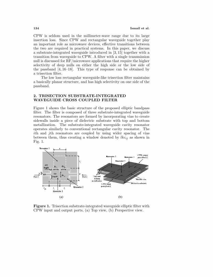
Figure 1 shows the basic structure of the proposed elliptic bandpassfilter. The filter is composed of three substrate-integrated waveguideresonators. The resonators are formed by incorporating vias to createsidewalls inside a piece of dielectric substrate with top and bottommetallization. The substrate-integrated waveguide cavity resonatoroperates similarly to conventional rectangular cavity resonator. Theith and jth resonators are coupled by using wider spacing of viasbetween them, thus creating a window denoted by lkcij as shown inFig. 1.
(a) (b)
Figure 1. Trisection substrate-integrated waveguide elliptic filter withCPW input and output ports, (a) Top view, (b) Perspective view.
Progress In Electromagnetics Research, PIER 85, 2008 135
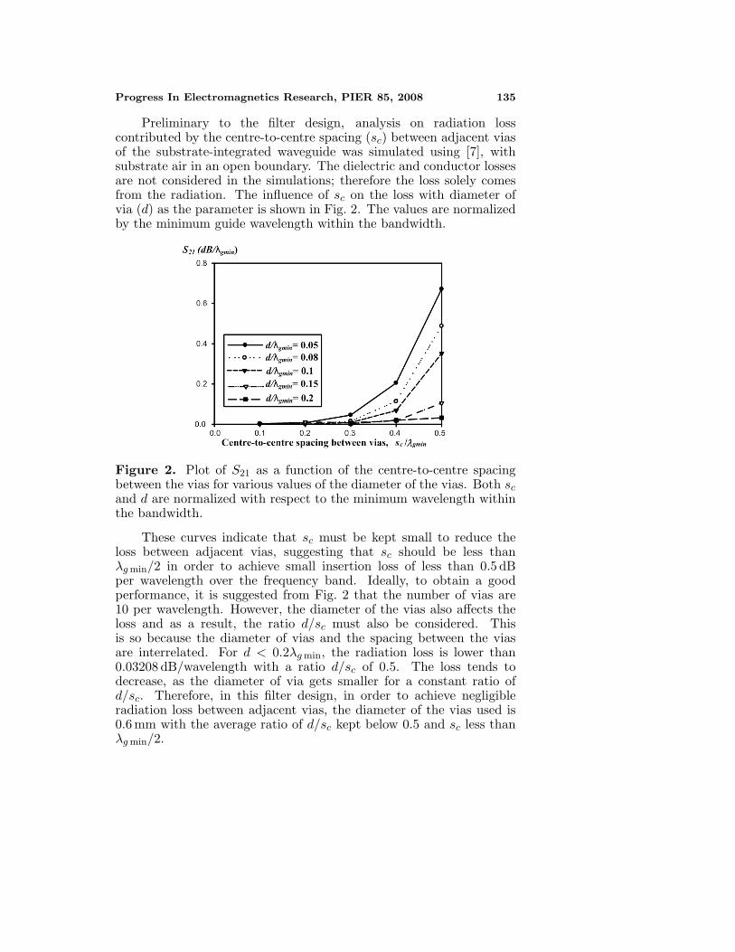
Preliminary to the filter design, analysis on radiation losscontributed by the centre-to-centre spacing (sc) between adjacent viasof the substrate-integrated waveguide was simulated using [7], withsubstrate air in an open boundary. The dielectric and conductor lossesare not considered in the simulations; therefore the loss solely comesfrom the radiation. The influence of sc on the loss with diameter ofvia (d) as the parameter is shown in Fig. 2. The values are normalizedby the minimum guide wavelength within the bandwidth.
Figure 2. Plot of S21 as a function of the centre-to-centre spacingbetween the vias for various values of the diameter of the vias. Both sc
and d are normalized with respect to the minimum wavelength withinthe bandwidth.
These curves indicate that sc must be kept small to reduce theloss between adjacent vias, suggesting that sc should be less thanλg min/2 in order to achieve small insertion loss of less than 0.5 dBper wavelength over the frequency band. Ideally, to obtain a goodperformance, it is suggested from Fig. 2 that the number of vias are10 per wavelength. However, the diameter of the vias also affects theloss and as a result, the ratio d/sc must also be considered. Thisis so because the diameter of vias and the spacing between the viasare interrelated. For d < 0.2λg min, the radiation loss is lower than0.03208 dB/wavelength with a ratio d/sc of 0.5. The loss tends todecrease, as the diameter of via gets smaller for a constant ratio ofd/sc. Therefore, in this filter design, in order to achieve negligibleradiation loss between adjacent vias, the diameter of the vias used is0.6 mm with the average ratio of d/sc kept below 0.5 and sc less thanλg min/2.

136 Ismail et al.
The input and output are coupled through CPW. Due to theirproximity, the cross coupling between resonators 1 and 3 exists. Anarrowband three-pole trisection filter has the equivalent circuit [5]shown in Fig. 3. The mutual inductance or coupling coefficient Mij
refers to the ith and jth resonator.
INPUT OUTPUTQe1 Qe3M12 M23
M13
C1 C2 C3
Port 1 Port 2Resonator
1Resonator
2Resonator
3
21L
21L
22L
22L
23L
23L
Figure 3. Equivalent circuit of a three-pole trisection filter [5].
The cross coupling, M13 will determine the selectivity at a finitefrequency. The external quality factors are denoted by Qe1 and Qe3 atthe input and output ports. A trisection filter will have an attenuationpole at one side of the passband, and it requires the resonators to beasynchronously tuned to give an asymmetric filter frequency response.Thus, the resonating frequency for each resonator may be different andmust be chosen to satisfy the filter requirements.
The angular resonant frequency of resonator i is given by [5]
ω0i =1√LiCi
= 2πf0i for i = 1, 2, 3 (1)
where Li and Ci are the inductance and capacitance values of theequivalent circuit.
To keep the physical configuration of the filter symmetricaleven though the frequency response is asymmetric, the followingassumptions are made [5],
M12 = M23, (2)Qe1 = Qe3 and (3)ω01 = ω03. (4)
Figure 4 shows the low pass prototype filter transformed from theequivalent circuit in Fig. 3. It uses J inverters with [5]
J12 = J23 = 1 (5)
J13 is the bypass inverter which represents the cross coupling. It isalso true that
g0 = g4, (6)

Progress In Electromagnetics Research, PIER 85, 2008 137
g1 = g3 and (7)B1 = B3, (8)
Here gi is the capacitance and Bi is the frequency invariant susceptanceof the lowpass prototype filter, while g0 and g4 denote the resistiveterminations at the input and output ports. This is shown in Fig. 4.
g0 g4jB1g1 g2 g3jB2
jB3
13J
12J = 1 23J = 1
Figure 4. Lowpass prototype filter using admittance (J) inverter forthree-pole trisection filter [2].
The unknown low pass element values may be determined by asynthesis method [6] or through an optimization process. Once theyare determined, the circuit parameters in Fig. 3 can be found by [5]
Qe1=b1g0
=ω0i
ω0g0
(g1
FBW+
B1
2
), (9)
Qen=bn
gn+1=
ω0n
ω0gn+1
(gn
FBW+
Bn
2
)and (10)
Mij |i�=j =Jij√bibj
=ω0
ω0iω0j
FBWJij√(gi + FBW Bi
2
) (gj + FBW
Bj
2
) . (11)
where n is the order of the filter.If the cross coupling is positive, i.e., M13 > 0 or J13 > 0, the
attenuation pole of finite frequency is on the high frequency side of thepassband, whereas if the cross coupling is negative, i.e., M13 < 0 orJ13 < 0, the attenuation pole of finite frequency is on the low side ofthe passband. We demonstrate that the filter configuration in Fig. 1has an attenuation pole of finite frequency above the passband owingto the cross coupling of resonators 1 and 3.

138 Ismail et al.
3. DESIGN OF SUBSTRATE-INTEGRATEDWAVEGUIDE FILTER WITH CPW INPUT ANDOUTPUT PORTS
For our demonstration, the filter is designed to meet the followingspecifications; centre frequency = 10 GHz, bandwidth of passband =0.3 GHz (fractional bandwidth of 3%), return loss in the passband ≤−20 dB and rejection > 20 dB for frequencies ≥ 10.32 GHz. Theelement values of the low pas prototype [8] filter are found to beg1 = g3 = 0.68334, g2 = 1.38933, B1 = B3 = 0.131, B2 = −0.89316,J12 = J23 = 1.0, J13 = −0.51059.
Having obtained the element values [8], the design parameters forthe X-band trisection filter are calculated as follows [8]:
Resonant frequency for resonator 1 and 3;f01 = f03 = 9.971 GHz,Resonant frequency for resonator 2;f02 = 10.0969 GHz,External quality factor;Qe1 = Qe3 = 22.778,Coupling coefficient for resonator 1, 2 and 3;M12 = M23 = 0.030792, M13 = −0.022416.Shown in Fig. 5 is the theoretical frequency response of the filter.
-80
-70
-60
-50
-40
-30
-20
-10
0
8 8.5 9 9.5 10 10.5 11 11.5 12
Frequency (GHz)
Mag
nit
ud
e (d
B)
Insertion loss (S11)
Return loss (S21)
S21
S11
Figure 5. Theoretical response of the substrate-integrated waveguidetrisection filter with an attenuation pole on the high side of thepassband.

Progress In Electromagnetics Research, PIER 85, 2008 139
The dimension of the transition determines the external qualityfactor. The external quality factor Qe for resonator 1 and 3 iscalculated by using a 3-D electromagnetic simulator [7] using the modelshown in Fig. 6.
(a) (b)
Figure 6. Extracting Qe for the X-band via waveguide trisection filter,(a) Top view, (b) Perspective view (a = 15 mm, lcpw = 10 mm).
The Qe is controlled by changing the slot length of the CPW-to-waveguide transition. Qe is obtained from the simulation by [5]
Qe =f0
f−3 dB(12)
where f0 is the resonant frequency of the resonator and f−3 dB is the3 dB bandwidth centre at the resonant frequency.
Figure 7 shows the simulated Qe with a resonant frequency of10 GHz. The Qe gradually decreases as the slot length becomeslarge. According to Fig. 7, as required for the filter specification,Qe1 = Qe3 = 22.78 is obtained at slot length = 1.72 mm. Fig. 8and Fig. 9 show the model to calculate the cross coupling betweenresonator 1 and 3, and the coupling between adjacent resonators 1 and2, respectively.
The length of the window lkcij as depicted in Fig. 8 and Fig. 9controls the degree of coupling between two resonators. The length l1and l3 in Fig. 8 for resonator 1 and 3 are tuned so that it has a resonantfrequency of 9.97 GHz as calculated in (1).
To extract the coupling coefficient between adjacent resonators(M12 = M23) in Fig. 9, resonator 1 and 2 is asynchronously tuned toeach individual resonant frequency. For resonator 2, l2 is optimized togive a resonating frequency of 10.09 GHz.
The coupling coefficient M12 can be calculated using (13) for

140 Ismail et al.
23.5
23.0
22.5
22.0
21.5
21.0
20.5
20.01.65 1.70 1.75 1.80 1.85 1.90 1.95 2.00
Qe
slot length (mm)
Figure 7. Qe with variation of slot length for the narrowband X-bandsubstrate-integrated waveguide trisection filter.
(a) (b)
Figure 8. Plane view of the model to calculate the coupling coefficient,M13 for resonator 1 and 3, (a) Top view, (b) Model used in thesimulator.
asynchronously tuned coupled resonators [5]
kij =12
(f02
f01+
f01
f02
) √√√√f22 − f2
1
f22 + f2
1
−(f202 − f2
01
f202 + f2
01
)(13)
where f01 and f02 is the resonating frequency for the ith and jthresonator respectively with f1 and f2 are the two frequency peaks.Since resonator 1 and 3 is synchronously tuned to have the sameresonant frequency, the cross coupling coefficient between the tworesonators, namely M13 in Fig. 8 can be calculated using (14) [5].
kij =f2
e − f2m
f2e + f2
m
(14)

Progress In Electromagnetics Research, PIER 85, 2008 141
where fe and fm are two resonant frequencies with perfect electric andmagnetic planes at the center.
Figure 10 shows the coupling coefficients Mij with various valuesof lkcij , obtained using an electromagnetic CAD simulator [7]. Thelarger coupling is obtained for the larger spacing lkcij . Accordingto Fig. 10(a), the coupling coefficients M12 = M23 = 0.031 canbe obtained at lkc12 = lkc23 = 5.4 mm, while the cross couplingcoefficients M13 = 0.022 is obtained at lkc13 = 4.09 mm as requiredby the filter specification.
a
a
lj
li
lkcijPORT1
1.0
2.0
1.02.0
RESONATOR1
RECTANGULARWAVEGUIDE INPUT
AND OUTPUTPORTS
PORT 2
RESONATOR2
METALLICVIAS
(a) (b)
Figure 9. Plane view of the model to calculate the coupling coefficientM12 for resonator 1 and 2, (a) Top view, (b) Model used in thesimulator.
(a) (b)
Figure 10. Simulated (a) coupling coefficient for resonator 1 and 2,(b) cross coupling between resonator 1 and 3.

142 Ismail et al.
Using the initial parameters of slot length and lkcij obtainedfrom the calculations above, the filter dimensions are tuned to realizethe required filter response for the substrate-integrated waveguidetrisection filter.
The dimensions of the X-band substrate-integrated waveguidetrisection filter, according to the simulation that will satisfy thespecifications are shown in Table 1. Note that the value of slot lengthand lkcij , are very close to the initial values as expected.
Table 1. Dimensions of an X-band substrate-integrated waveguideelliptic trisection filter.
Parameter Dimension (mm)Width of cavity, a 15Substrate thickness, b 3.175Metal thickness, t 0.035Centre conductor of CPW, S 3.0Slot of CPW, w 0.27Length of CPW, lcpw 10
Length of bent slot, slot length1.4
(Initial value = 1.72)Width of bent slot, slot height 1.2Length of cavity 1 and 3, l1 = l3 13.1Length of cavity 2, l2 13.6Coupling window between adjacent 5.7resonators, lkc12 = lkc23 (Initial value = 5.4)Coupling window for cross coupling, 4.1lkc13 (Initial value = 4.09)
The filter has been fabricated on an RT/Duroid 5880 substratewith a relative dielectric constant, εr of 2.2 and a thickness of 5.68 mm.SMA connectors are attached to the CPW lines at the input and outputports in order to measure the filter using a network analyzer.
The simulated and measured frequency responses of the trisectionfilter are shown in Fig. 11.
The simulation results have included the dielectric and conductorlosses (tan δ = 0.0009 and σ = 5.813×10⁷ S/m). According to Fig. 11,the measured insertion loss of 3.13 dB is obtained for the trisection filter

Progress In Electromagnetics Research, PIER 85, 2008 143
Figure 11. Simulated and measured frequency response for the X-band via waveguide elliptic trisection filter.
at a centre frequency of 10.09 GHz with the return loss better than−13.5 dB for the passband. An attenuation pole at almost exactlyat 10.35 GHz is obtained, fulfilling the specification. Fabricationtolerances (±0.02 mm), conductor loss, the tolerance in the dielectricpermittivity (±0.02) and connector mismatch have contributed to thetotal loss of the measured frequency responses. These are untunedresults, nonetheless prove that the design method are correct andmanifest the total potential in producing good agreement betweensimulated and measured results with proper tuning.
Even though the sidewalls of the resonators are composed of arraysof vias (or metallic posts), which involve spacings between them, theradiation loss due to the spacings are made sure to have very littleeffect on the overall loss performance.
4. CONCLUSIONS
An X-band trisection substrate-integrated waveguide elliptic filter hasbeen designed and fabricated. The simulated frequency responsesagree well with the measured. The potential of having bothplanar and non-planar (waveguide) circuits on a single substrate hasbeen demonstrated with a filter with transition designs to coplanarwaveguide.
Benefits for more complex microwave filters such as trisection

144 Ismail et al.
filters can be achieved with the proposed design of utilizing substrate-integrated waveguide in this paper.
REFERENCES
1. Herrick, K. J., T. A. Schwartz, and L. P. B. Katehi, “Si-micromachined coplanar waveguides for use in high-frequency cir-cuits,” IEEE Transactions on Microwave Theory and Techniques,Vol. 46, No. 6, 762–768, June 1998.
2. Park, J.-H., C.-W. Baek, S. Jung, et al., “Novel microma-chined coplanar waveguide transmission lines for application inmillimetre-wave circuits,” Jpn., J. Apply. Phys., Vol. 39, Part 1,No. 12B, 7120–7124, December 2000.
3. Deslandes, D. and K. Wu, “Integrated transition of coplanar torectangular waveguides,” IEEE MTT-S Digest, 2001.
4. Hong, J.-S. and M. J. Lancaster, “Microstrip cross-coupled trisec-tion bandpass filters with asymmetric frequency characteristics,”IEE-Proc. - Microwave Antennas Propagation, Vol. 146, No. 1,84–90, February 1999.
5. Hong, J.-S. and M. J. Lancaster, Microstrip Filters forRF/Microwave Applications, John Wiley and Sons Inc., 2001.
6. Hershtig, R., R. Levy, and K. Zaki, “Synthesis and design of cas-caded trisection (CT) dielectric resonator filters,” Proceedings ofEuropean Microwave Conference, 784–791, Jerusalem, September1997.
7. CST Microwave Studio Version 5.3.8. Jayyousi, A. B. and M. J. Lancaster, “A gradient-based
optimization technique employing determinants for the synthesisof microwave coupled resonators,” IEEE MTT-S Digest, Vol. 2,1369–1372, June 2004.
9. Zhao, L.-P., X. Zhai, B. Wu, T. Su, W. Xue, and C.-H. Liang,“Novel design of dual-mode bandpass filter using rectangularstructure,” Progress In Electromegnetics Research B, Vol. 3, 131–141, 2008.
10. Ghorbaninejad, H. and M. Khalaj-Amirhosseini, “Compactbandpass filters utilizing dielectric filled waveguides,” Progress InElectromegnetics Research B, Vol. 7, 105–115, 2008.
11. Zhang, J. and T. Y. Hsiang, “Dispersion characteristics ofcoplanar waveguides at subterahertz frequencies,” Journal ofElectromagnetic Waves and Application, Vol. 20, No. 10, 1411–1417, 2006.

Progress In Electromagnetics Research, PIER 85, 2008 145
12. He, Z. N., X. L. Wang, S. H. Han, T. Lin, and Z. Liu, “Thesynthesis and design for new classic dual-band waveguide band-stop filters,” Journal of Electromagnetic Waves and Application,Vol. 22, No. 1, 119–130, 2008.
13. Khalaj-Amirhosseini, M., “Microwave filters using waveguidesfilled by multilayer dielectric,” Progress In ElectromagneticsResearch, PIER 66, 105–110, 2006.
14. Sotoodeh, Z., B. Biglarbegian, F. H. Kashani, and H. Ameri, “Anovel bandpass waveguide filter structure on SIW technology,”Progress In Electromagnetics Research Letters, Vol. 2, 141–148,2008.
15. Che, Q.-Q., C.-X. Li, D.-P. Wang, L. Xu, and Y. L. Chow,“Investigation on the ohmic conductor losses in substrate-integrated waveguide and equivalent rectangular waveguide,”Journal of Electromagnetic Waves and Application, Vol. 21, No. 6,769–780, 2007.
16. Zhang, J., J.-Z. Gu, B. Chiu, and X.-W. Sun, “Compact andharmonic suppression open-loop resonator bandpass filter withtri-section SIR,” Progress In Electromagnetics Research, PIER 69,93–100, 2007.
17. Mohammad Amjadi, S. and M. Soleimani, “Design of band-passwaveguide filter using frequency selective surfaces loaded withsurface mount capacitors based on split-field update fdtd method,”Progress In Electromagnetics Research B, Vol. 3, 271–281, 2008.
18. Zhang, J., B. Cui, S. Lin, and X.-W. Sun, “Sharp-rejection low-pass filter with controllable transmission zero using complemen-tary split ring resonators (CSRRs),” Progress In ElectromagneticsResearch, PIER 69, 219–226, 2007.