dcudoras.dcu.ie/18182/1/jason_roche_20130119110245.pdf · 5.2 nitrogen modification of band...
TRANSCRIPT

Characterisation of Ultra-thin
Oxynitride dielectric layers
Jason Roche (B.Sc.)
School of Physical Sciences
Dublin City University
A thesis submitted to
DCUOllscoil Chathair Bhaile Atha Ciiath
For the degree of
Doctor of Philosophy
Research Supervisor
Dr. Greg Hughes
March 2003

Declaration
I hereby certify that this material, w hich I now subm it for assessm ent on the programme
o f study lead ing to the award o f doctor o f P h ilosop h y is entirely m y ow n work and has
not been taken from the work o f others save and to the extent that such work has been
cited and acknow ledged w ith in the text o f m y ow n work.
Signed: ÜÎVN Id Number: 98970577
Date: \ i ^ _____
i i
I

Contents
Title page iDeclaration iiContents iiiAbstract ixAcknowledgements xTable of Acronyms xi
Chapter I Introduction 1
1.0 Transistor History and the birth of the MOSFET 1
1.1 Si(l 00) A technologically important surface 2
1.2 Oxidation of silicon 3
1.3 SiOx Chemical transition region 4
1.4 Structural transition region 5
1.5 Limitations 7
1.6 Thesis Motivation 8
1.7 Thesis Layout 9
1.8 References for chapter I 11
Chapter n Theory of experimental techniques 13
2.0 Photoemission Introduction 13
2.1 Photoemission Process 15
2.1.1 X-ray production 16
2.1.2 Spin-orbit splitting 17
2.1.3 The chemical shift 19
2.1.4 Koopmans ’ Theorem 21
2.1.5 Surface Sensitivity 22
2.1.6 Final State Effects 23
2.1.7 Peak broadening 23
iii
2.2 XPS experimental setup/Data Acquisition 25
2.3 Data Analysis 31
2.4 Quantification 34
2.4.1 S1O2 Overlayer model 36
2.4.2 Oxide Stoichiometry 37
2.4.3 Quantification standard 39
2.4.4 Hydrocarbon contamination 42
2.4.5 Oxide Charging 43
2.5 Si02 Chemical Depth Profile 44
2.5.1 Inert Ion Bombardment 45
2.5.2 Wet chemical profiling 48
2.5.3 Angular Resolved XPS 49
2.6 Atomic Force Microscopy 52
2.6.1 Contact Mode AFM 54
2.6.2 Non-Contact Mode AFM 56
2.6.3 Tapping Mode AFM 57
2.7 Low Energy Electron Diffraction 61
2.8 Synchrotron Radiation 66
2.8.1 NSLS U4A Beamline Characteristics 68
2.8.2 Synchrotron considerations 70
2.9 References for Chapter II 73
iv

Chapter III Chemical characterisation of thin SiON and S i0 2 76
films using X-ray photoelectron spectroscopy
3.0 Introduction 76
3.1 Si02 As-received 77
3.2 Fitting parameters 79
3.3 Ar Ion Bombardment 84
3.3.4 Discussion of results 93
3.4 S i02 Chemical Depth Profile using weak HF acid 94
3.4.1 Quantification concerns 97
3.4.2 Discussion of results 104
3.5 HF / Ar+ bombardment comparison 105
3.5.1 Discussion of results 108
3.6 Oxynitride Analysis Overview 109
3.7 SiON As-received 118
3.71 Wet Chemical Depth Profile for 5.5nm oxynitride 120
3.7.2 Wet Chemical Depth Profile for 3.3nm oxynitride 128
3.7.3 Discussion of results 132
3.8 Conclusion 135
3.9 References for Chapter IQ 137
v
Chapter IV A Chemical state investigation of the SiON and S i0 2 140
interface using synchrotron soft X-ray photoelectron
spectroscopy
4.0 Introduction 140
4.1 Theoretical interpretation of interface 141
4.2 Re-examination o f SÌ2P chemical shift interpretation 144
4.3 Wet chemical processing 147
4.4 Surface Morphology / Oxidation induced roughness 150
4.5 Atomic Force Microscopy Analysis 156
4.5.1 Discussion of results 169
4.6 SÌO2 Synchrotron Analysis Overview 169
4.6.1 SÌO2 Experimental 175
4.6.2 Interface state distribution 182
4.6.3 Discussion of results 192
4.7 SiON Synchrotron Analysis Overview 193
4.7.1 SiON Experimental 198
4.7.2 Discussion of results 206
4.8 Conclusion 207
4.9 References for Chapter IV 209
v i
Chapter V X-ray Absorption and Emission spectroscopy of 213
ultra-thin oxides
5.0 Soft x-ray Emission Spectroscopy 213
5.1 Soft x-ray Absorption Spectroscopy 216
5.2 Nitrogen Modification of band structure 218
5.3 Experimental results 222
5.4 Discussion of results 226
5.5 Conclusion 227
5.6 References for Chapter V 228
Chapter VI Core-level Photoemission studies of the Sulphur 229
terminated Si(100) and Ge(100) surfaces
6.0 Introduction 229
6.1 Si(100) bulk and surface structure 229
6.2 LEED structure 236
6.3 Photoemission 238
6.4 Group IV semiconductor surface passivation 240
vii
6.5 S i(l00) experimental 242
6.5.1 Electron beam heating 243
6.5.2 Sulphur cell 244
6.5.3 Clean Si(100) 246
6.5.4 Sulphur Deposition 247
6.5.5 Discussion of results 250
6.6 Ge( 100) Overview 253
6.61 Ge(100)-(2xl) Surface Core level Shifts 255
6.62 S passivation of Ge(100) 258
6.63 S/Ge(100) Experimental 260
6.64 Sulphur deposition 261
6.65 Discussion of results 265
6.7 Conclusion 266
6.8 References for Chapter VI 267
Chapter VI Comparisons, Conclusions and Further Work 270
7.0 Overview of thesis 270
7.1 References for Chapter VII 274
viii
A b stract
This thesis is an investigation of thin oxides formed on Si(100) in a device manufacturing environment. Chemical analysis was performed on SiC>2 and SiON films comprising a sample set with thicknesses spanning 5 to 20 nm. Chemical characterisation, using XPS confirmed film quality through the consistency in stoichiometry, thickness, elemental composition and peak parameters for the as- received wafers. ARXPS measurements provided a qualitative interpretation of the interface and suggest suboxides are localised near the interface. In synchrotron studies using soft X- rays, both tunable photon energy and high resolution revealed precise information on the chemical and spatial distribution of interfacial suboxides and nitrides in the S i02 and SiON film respectively. It was possible to identify the presence of hydrides at both interfaces. For the oxynitrides the presence of a nitrogen rich region at the surface and interface is supported by the XPS and synchrotron studies.
X-ray Absorption Spectroscopy XAS and X-ray emission Spectroscopy XES measurements were performed using synchrotron radiation in order to profile the partial density of states of the nitrogen and the oxygen in the valence band and conduction respectively. While the 8.5 eV energy bandgap between the PDOS associated with the oxygen in the valence band and conduction band agrees with the Si0 2 bandgap, the equivalent energy gap for the nitrogen related states is approximately 5.5 eV.
The surface reconstruction of sulphur passivated Si(100) and Ge(100) surfaces were investigated by LEED and synchrotron soft X- ray photoemission spectroscopy. These studies were an attempt to ideally terminate these group IV (100) surfaces by a monolayer of divalent group VI element. Sulphur was deposited onto the atomically clean Si(100) (2x1) from an electrochemical cell. While the resulting surface displayed a ( lx l) LEED pattern indicating ideal termination, the core level photoemission spectra reveled the presence both +1 and +2 oxidation states. Analysis of these spectra concluded that the sulphur coverage approximated to % of a monolayer meaning that the surface termination was non-ideal. LEED results from the study of sulphur deposition on the clean Ge(100) surface again revealed the presence of a ( lx l) surface reconstruction. The photoemission results from the Ge3d displayed the presence of all four Ge oxidation states again indicating the non-ideal termination of the surface.
The samples examined in this thesis were realised in an industrial fabrication process. Precise knowledge of the nature of the sample history is limited to that which is expressed in the thesis.

Acknowledgements
For patience, encouragement, and understanding I’m indebted to Dr. Greg Hughes
who’s enthusiasm for and insight into the field of Surface Science will always be a
source of inspiration.
On the surface, it’s a crazy quantum world out there, but it’s made a little easier thanks
to Dr. Tony Cafolla.
“ To learn is to grow ”. To my parents Ann and Bernard, for more than word can say,
thank you.
Where would I be without the love and support of my brother Bernard, sister Elaine and
nephews Uilliam Caoilfhinn and baby Brannach.
Many thanks also to the lads in the lab both past and present.
“In the beginning there was” Clodagh and me. After four years of scans, coffee, beer,
arguments, laughter, tears and a fire, we, “still haven’t found what we’re looking for”.
Also, from the Lab a big thanks to Darren, Philippe, and Eilish.
Cheers to “little Phil” Ryan for help at the NSLS . He throws ball like a g ir l!.
Finally I would like to acknowledge the financial help and support from Intel Ireland
and Enterprise Ireland under the applied grants scheme.
Famous last words: “Silicon, that’s just like sand?”
x

Table of Acronyms
AES Auger Electron SpectroscopyAFM Atomic Force MicroscopyFWHM Full Width Half Maximum[MFP Inelastic Mean Free PathLEED Low Energy Electron DiffractionMOSFET Metal Oxide Semiconductor Field Effect TransistorNRA Nuclear Reaction AnalysisPDOS Partial Density of StatesRBM Random Bonding ModelRBS Rutherford Back ScatteringSICT Structure Induced Charge TransferSIMS Secondary Ion Mass SpectroscopyUHV Ultra High VacuumXAS X-ray Absorption SpectroscopyXES X-ray Emission SpectroscopyXPS X-ray Photoelectron Spectroscopy
Chapter 1
In trodu ction
1.0 Transistor History and the birth of the MOSFET
The modern semiconductor industry was born in the discovery of the bipolar transistor
at Bell Labs in 1947 by Shockley, Bardeen and Brattain [1], a solid-state switch that
replaced vacuum tubes in the early implementation of binary logic. Continued
improvement in material science, computer architecture and device design lead to the
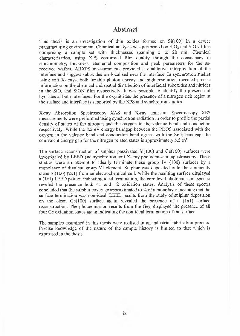
emergence of the MOSFET in the sixties [2], A MOSFET as shown in figure 1.0, it is a
high speed switch which works when a voltage applied to the gate terminal (G) giving a
potential difference across an insulating oxide, results in an induced channel of
accumulated minority charge (n or p type) carrier underneath the oxide facilitating
current flow from the source (S) to drain (D) terminal. The evolution of this device from
then was envisioned by Gordon Moore, “the number of components on integrated chips
Drain
Depletion p1sr
Figure 1.0: A cross section of an enhancement type n-channel MOS transistor [3],
1
would double every 18 months for the next ten years”. MOS technology moved from p
to n and then to CMOS through continuous improvements in areas like lithography and
contamination control [2]. Despite lower performance, high processing complexity and
a tendency to “lock up” in high current mode, lower power dissipation facilitating
higher integration allowed CMOS to surpass bipolar technology and become the key
“building block” of the modem semiconductor industry [4].
1.1 Si(100) A technologically important surface
In today’s global semiconductor device fabrication industry the integrity of silicon’s
oxide plays a critical role. The oxidation of silicon at high temperature in an oxygen
ambient is a remarkable process, resulting in a stoichiometric (O/Si, 2:1) amorphous
film in which Si atoms form a tetrahedral diamond-like lattice similar to crystalline
silicon but now each silicon is connected to four other silicon atoms not directly, but via
linear Si-O-Si bonds. At MOS operating temperatures this protective oxide film is;
mechanically stable, electrically insulating (almost a perfect dielectric) and chemically
protective. Germanium and gallium arsenide, materials whose inherent electrical
properties are superior to silicon’s are at a disadvantage because of the inferior
properties of their oxides: germanium dioxide is water soluble and the oxidation of
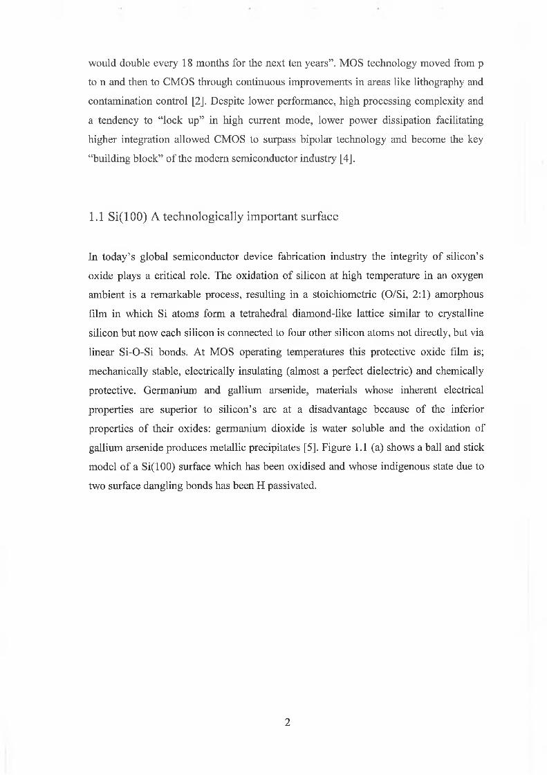
gallium arsenide produces metallic precipitates [5]. Figure 1.1 (a) shows a ball and stick
model of a Si(100) surface which has been oxidised and whose indigenous state due to
two surface dangling bonds has been H passivated.
2
(a) •# m
# 0
» •• •
I• •
# •• •
• •
® Oxygen • :Silicon ® Hydrogen
Figure 1.1: (a) Si(100) Ideal Termination, (b) Actual interface (Lu [6 ])
This represents an ideal interface, as it is atomically abrupt and chemically inert.
Si(100) is the preferred substrate orientation for device fabrication due to it’s lower
defect density and post oxidation suboxide distribution, relative to S i( l l l ) where a
rougher, more distributed interface is obtained owing to the greater number of
indigenous defect states (Si1+ and Si3+).
1.2 Oxidation of silicon
At a clean Si(100) surface, silicon atoms at the lattice boundary have a reduced
coordination number and reconstruct to reduce surface energy. Surface passivation with
hydrogen terminates the silicon dangling bonds and renders the surface chemically inert.
When heated to 1000 °C the silicon lattice, through as many degrees of freedom as
possible, violently dissipates the thermal energy. The surface reconstruction is broken.
If oxygen is present, a complex two-stage reaction takes place, which was first
described by Deal and Grove [7] where an oxide layer is formed as the underlying
silicon is oxidised.
• * •I
• • •
• • •
• • •
(b): Oxygen
G t ’ : SiliconJHf* - ■
a i * l> S* * !' 'Vt,v a , <>, 1; L ■
. .V j ; /- r Yv. f V N-.ys r " " " I I-*-'t '. ■" ( i f f v'' . , ; I I - <' it. . ■ • /! •• i 1
' ' , v' v /♦ AOV i - A I * A I > t * A s
? 1 ’ A \— -
3

Si + O2 <=> Si02
Atomic transport during thermal oxidation occurs via interstitial diffusion of molecular
oxygen across the growing oxide, without reacting with it, and subsequent reaction with
Si at the oxide/Si interface promoting growth [8]. The oxidation kinetics is controlled by
“interface reactions” in the initial stages and by “diffusion of the reacting species” once
a thick film has been grown. The “marriage” between the oxide and underlying film is
not without “strain”. The transition from bulk crystalline silicon to bulk amorphous
silicon dioxide occurs at an interface where the density of silicon atoms in crystalline Si
is twice that in glassy Si0 2 , so the silicon “lattice” must expand during oxidation due to
the insertion of an O atom into the Si-Si bond [9]. This lattice mismatch makes an
epitaxial relationship between the substrate and oxide hard to realise. Both compressive
and tensile stress result in the interfacial region consisting of buffer regions in which
there are both chemical and structural transitions in Si in terms of its bonding state and
geometry.
1.3 SiOx Chemical transition region
In Si(100)/Si02 and Si(l 11)/Si02 interfaces, the detection by photoemission of the non-
indigenous suboxides Si2+ and Si3+ respectively, indicates the existence of non-ideal
interfaces in both systems. By growing the oxides to different thickness and varying the
degree of surface sensitivity, photoemission studies can be used to determined the
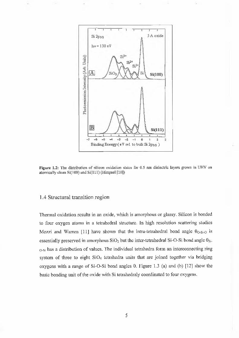
suboxides to be distributed within ~1 nm of the interface. Figure 1.2 (a) and (b) shows
the Si2P core level spectra from oxide layers grown in-situ to a thickness of 0.5 nm on
Si(100) and S i( l l l) substrates respectively [10]. The figure shows the presence of all
possible suboxide states in both systems but as will be described in chapter 4, the
different intensity distributions is related to the surface orientation.
4
Binding Energy ( eV re 1. to bulk Si 2p3/2 )
Figure 1.2: The distribution of silicon oxidation states for 0.5 nm dielectric layers grown in UHV on atomically clean Si(100) and S i ( l l l ) (Himpsel [10])
1.4 Structural transition region
Thermal oxidation results in an oxide, which is amorphous or glassy. Silicon is bonded
to four oxygen atoms in a tetrahedral structure. In high resolution scattering studies
Mozzi and Warren [11] have shown that the intra-tetrahedral bond angle 0o-si-o is
essentially preserved in amorphous SiC>2 but the inter-tetrahedral Si-O-Si bond angle 0si-
o-si has a distribution of values. The individual tetrahedra form an interconnecting ring
system of three to eight SiC>4 tetrahedra units that are joined together via bridging
oxygens with a range of Si-O-Si bond angles 0. Figure 1.3 (a) and (b) [12] show the
basic bonding unit of the oxide with Si tetrahedraly coordinated to four oxygens.
5
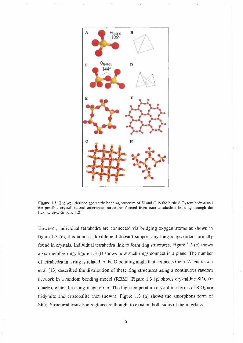
Figure 1.3: The well defined geometric bonding structure of Si and O in the basic S i0 2 tetrahedron and the possible crystalline and amorphous structures formed from inter-tetrahedron bonding through the flexible Si-O-Si bond [12],
However, individual tetrahedra are connected via bridging oxygen atoms as shown in
figure 1.3 (c), this bond is flexible and doesn’t support any long range order normally
found in crystals. Individual tetrahedra link to form ring structures. Figure 1.3 (e) shows
a six-member ring, figure 1.3 (f) shows how such rings connect in a plane. The number
of tetrahedra in a ring is related to the O bonding angle that connects them. Zachariassen
et al [13] described the distribution of these ring structures using a continuous random
network in a random bonding model (RBM). Figure 1.3 (g) shows crystalline SiC>2 (a
quartz), which has long-range order. The high temperature crystalline forms of S i02 are
tridymite and cristobalite (not shown). Figure 1.3 (h) shows the amorphous form of
S i02. Structural transition regions are thought to exist on both sides of the interface.
6

On the substrate side Haight and Feldman [14] in a non-destructive study of the
interface structure and stoichiometry, using ion backscattering channelling methods
NRA and RBS found that in the near interfacial region there is a zone with excess Si.
This Si corresponds to non-epitaxial layers within the single crystalline substrate. They
associated the result with a vertical displacement of two atomic layers of silicon next to
the interface. On the oxide side of the interface a structural transition region is thought
to exist above the suboxide layer. This Si02 layer is stoichiometric but the Si-O-Si bond
angle is reduced due to compressive stress associated with the interface. Grunthaner et
al [15] considered a structure induced charge transfer (SICT) model in which the charge
distribution in the Si-0 bond, as well as the in the ring, would be dependent upon the
inter-tetrahedral bond angle ©si-o-si and the ring size n. Bulk Si02 has a distribution of
Si-O-Si bond angles centred near 144°, similar to a-quartz and indicative of six Si
tetrahedra in a ring structure. In a region within 0.3 nm of the interface, a strained layer
induced by lattice mismatch is observed corresponding to a Si-O-Si bond angle
distribution centred near 120°, similar to the four-member ring structure of the Si02
polymorph coesite. Grunthaner resolved both the Ois and Si2P4+ photoemission peaks
into components corresponding to the bulk and strained regions. Although the SICT
model is well defined and a strained Si02 region above the interfacial region has been
revealed by both TEM studies and by a reduction in oxide etch rate [16]. Due to the
relative insensitivity to the chemical environment beyond the nearest neighbour
coordination shell, photoemission has little to say regarding the local or extended
structure of the oxide.
1.5 Limitations
As further reduction in MOSFET device dimensions require further reduction in oxide
thickness and channel length, the chemical and structural transitions discussed above
will constitute a larger fraction of the oxide. With the effect of these regions on device
performance not yet fully understood, Si02’s ability to sustain Moore’s law into the
future is not certain. Also in optical processing, lithographic improvements have
become diffraction limited and the cost of electron beam alternatives may outweigh the
gains. In addition, further device scaling is already limited by leakage current through
7
the oxide and short-channel effects [2]. Solutions have come forth in the form of device
design revision, as in (i.e. silicon on insulator SOI) and the re-engineering of the oxide
material in the form of high k dielectrics. A material with a higher dielectric constant
than S i02, can have a thicker oxide (thus reducing the tunnelling problem) while
maintaining the same capacitive thickness. Unfortunately many higher k dielectrics
Y2O3, Ce0 2 , Ta2 and Ti0 2 have bandgaps smaller than Si0 2 and so the gains from
increased thickness are undermined by the exponential dependence of leakage current
on the bandgap related barrier height. Also, a number of these materials are not
thermally stable on silicon and suffer from a large number of interface density of states
[2], So far N incorporation in Si0 2 either directly during oxidation (N20 or NO) or in a
post oxidation anneal (N2O, NO or NH3) has improved device operation by: acting as a
barrier to Boron diffusion at the gate/oxide interface, increasing the oxide dielectric
constant in the bulk oxide and reducing interface strain at the oxide/substrate interface.
1.6 Thesis Motivation
The pursuit of a complete understanding of the oxide layer resulting from thermal
oxidation of silicon encompassing both the interface and bulk film properties has been
on going and will continue, for many years. Si0 2 films have been characterised by many
different experimental techniques whose results give information on film thickness
(Elliposimetry [17], TEM [18], ARXPS [19-25], XPS [26-27], NRA), chemical state
(XPS, AES, FTIR), chemical composition (SIMS), micro roughness (AFM, STM) and
interface structure (synchrotron radiation photoemission).
The processes used to realise Si0 2 films on Si are diverse and range from; thermal
oxidation, wet chemical oxidation, electrochemical anodization, chemical deposition
(CVD, PECVD, JVD, ALD), physical deposition (i.e. LEII). Also many oxides are
grown in-situ on atomically clean silicon surfaces in ultra-high vacuum. It is not
surprising therefore to find discrepancies in the literature among researchers trying to
converge on a universal description of the Si/Si02 system, for samples with such
different sample histories.
8
The samples studies in this thesis are thermal oxides grown in an oxygen ambient at
room temperature in a class 100 clean room (i.e. 1 p.m sized contaminant per cubic
meter) on a 200 mm hydrogen passivated Si(100) wafer in a 0.18 p.m (channel length)
fabrication process which is designed to produce high quality oxide films. This provides
the confidence that any 1 x 1 cm sample of such a production wafer analysed is identical
both chemically and electrically to any other. After all, a 0.1 nm thickness variation in
oxide thickness would result in an order of magnitude variation in tunnelling current in
a final MOS structure. Within the capabilities of conventional XPS and synchrotron
radiation sources, this thesis seeks to characterise the dielectric layer chemically using
photoemission.
1.7 Thesis Layout
In chapter 2 both the theory of and implementation details, of the experimental
procedures used in this thesis are outlined and discussed.
The aim of chapter 3 is to investigate the quality of dielectric layers spanning the thin
(<10 nm) to ultra-thin (<5 nm) thickness regimes chemically. To that end chapter 3
undertakes the chemical characterisation using XPS to gauge the chemical composition,
chemical state and thickness of the as received films. Depth profiling using inert ion
bombardment and wet chemical etching using weak HF solutions, in conjunction with
ARXPS is used to “better illuminate” the interface which is otherwise attenuated by the
overlying oxide. Also, from wet chemical profiling of the oxynitrides the spatial
distribution and bonding environment of nitrogen is measured.
The large energy window and large sampling depth of XPS allowed the high binding
energy peaks (N and O) to be sampled and the substrate to be seen through the thick
(6.5 and 5.5 nm) oxide layers allowing values of thickness and stoichiometry to be
calculated. The consistency in these values along with the homogeneity of the elemental
composition has allowed the high quality of the dielectric layer to be ascertained.
9
In chapter 4 the chemical state and distribution of interfacial suboxides in both SiCVSi
and SiON/Si interfacial regions were investigated using the tuneable surface sensitivity
and high resolution capabilities of a synchrotron radiation source. A comparison of the
interfacial regions in the nitrided and non-nitrided layer was made to elucidate possible
interfacial Si-N related bonding. The dielectric layers were thinned wet chemically
using dilute HF acid etching in order to realise an oxide thickness comparable to the
small sampling depth of the photon energies used in the study. AFM measurements
were undertaken in order to gauge the extent of wet chemical etch induced surface
roughness.
Chapter 5 was based on a collaboration with Boston University where XES and XAS
measurements were performed at a synchrotron (NSLS) on the oxide and oxynitride
layers. The layers were etched to thickness comparable to those in chapter 4. The
measurements gave information about the element specific partial density of states.
From comparison of the partial densities of valence and conduction band states for
oxygen and nitrogen in the interfacial region, the role of nitrogen incorporation at the
interface and its effect on the band off-sets was investigated.
In Chapter 6 the potential of sulphur to ideally terminate the surface re-constructions of
the clean Si(100) and Ge(100) surfaces in-situ using an UHY compatible
electrochemical cell was investigated. The surface microstructure and chemical state
were interpreted through the surface core level shifts, which were measured using
synchrotron soft X-ray core level photoemission and LEED.
In Chapter 7 an overall conclusion and discussion of the thesis work undertaken is
presented and possible future work is considered.
10
1.8 References for Chapter I
1 S. M. Sze, Physics of Semiconductor Devices. New York: John Wiely & Sons 1969.
2 D. A. Buchanan, IBM J. RES. DEVELOP.,43 (1999),
3 B.G. Strectman, Solid State Electronic Devices: Prentice/Hall International 1980.
4 R. D. Issac, IBM J. Res. Develop., 44 (2000), 369
5 F. J. Feigl, Physics Today, Oct. (1996), 47
6 Z. H. Lu et al, Appi. Phys. Lett. 63 (1993) 2941
7 B. Deal, A. Grove, J. Appi. Phys. 36 (1965) 3770
8 I. J. R. Baumvol, Surf. Sci. Rpts. 36 (1999) 1
9 Z. Lu, S. Tay, R. Cao, Appi. Phys. Lett. 19 (1995) 2836
10 F. Himpsel, F. McFeely, A. Ibramimi, J. Yarmoff, G. Hollinger, Phys. Rev. B38
(1988)6084
11 L. Mozzi and B. Warren, J. Appi. Crystallogr. 2 (1969) 164
12 West Virginia University Department of Geography and Geology
http : //www. geo. wvu.edu/~langv/Geol284/Min8 IgFels/tsld03 0. htm
13 W. H. Zachariassen, J. Am. Chem. Soc. 54 (1932) 3841
14 R Haight, L Feldman, J. Appi Phys. 53 (1982) 4884
15 F. Grunthaner, P. Grunthaner, R. Vasquez, B. Lewis, J. Maserjian, A Madhukar, Phys
Rev. Lett. 43 (1979) 1683
16 S. Miyazaki, T. Tamura, m. Ogasawara, H. Itokawa, H. Murkami M. Hirose, Appi.
Surf. Sci. 159 (2000) 75
17 E. Irene, Crit. Rev. Solid State Mater. Sci. 14 (1998) 175
18 A. Carim, R. Sinclair, Chemical and Electrochemical Processes 3 (1987) 741
19 S. Spruytte, D. Pantelidis J. Vac. Sci. Technol. A19 (2001) 603
20 L. Chen, R W. Hoffman J. Vac. Sci. Technol. A l l (1993) 2303
21 J. E. Fulghum, Surf. Interface Anal. 20 (1993) 161
11

22 T.D. Bussing, P.M. Holloway J. Vac. Sci. Technol. A3 (1985) 1973
23 W.A.M Aarnink, Appi. Surf. Sci. 45 (1990) 37
24 M.F. Ebel, Spectrochimica Acta, 39B (1984) 637
25 P. J. Cumpson J. Electron Spectrosc. Relat. Phenom. 73 (1995) 25
26 D.F. Mitchell, Surf. Interface Anal 21 (1994) 44
27 Z.H. Lu, S.P. Tay L.c. Feldman B. Brar, Appi. Phys. Lett. 71 (1997) 2764
12

Chapter 2
Theory of Experimental Techniques
2.0 Photoemission Introduction
In the condensed environment of a solid, the overlap and nature of electron bonds, along
with the lattice structure, decide the solid’s electronic properties. In a metal, the
abundance of de-localized “free” electrons “screen” the effect of the lattice, resulting in
a free electron dispersion relation (parabolic E vs. k) for its wavevector. In a
semiconductor the “unscreened” periodic lattice diffracts (forbids) certain wavevector
values resulting in band gaps. Photoemission’s ability to probe electron dispersion by
interrogating the momentum of occupied states, and electron bond interactions from
binding energies arises from both the quantised and wave like nature of electromagnetic
radiation and matter as shown in figure 2.0.
(a)-Vacuum Level
Conduction Band
Fermi Level
Cote Levels <c
(b)
vacuum
k|| (bxOt
‘ J solid
XHi. ùntì
r V ‘
Ak|| (torf) = k)| =
►i h
Figure 2.0: a) Simplified representation o f the band structure o f a semiconductor where adjacent atomic wavefunctions overlap to form bands, b) Absorption o f a high-energy photon by a inner core electron can liberate it from the solid. The photoelectron emitted from the sample is refracted by the surface potential step. The parallel component o f the momentum is conserved during the transition, but the perpendicular component is not conserved due to the loss o f crystal periodicity along the surface normal.
13

When illuminated with light of suitable photon energy, an electron absorbs the
quantised photon energy in an “all or nothing process” in which total energy is
conserved, as borne out by the Einstein relation equation 2.0. Its wave nature is
conveyed via the de-Brogile relationship by its momentum and associated wavelength.
The termination of the solid presents an interface across which the component of the
photoelectron’s momentum tangential to the surface is conserved. The component of the
photoelectrons momentum normal to the surface is not conserved due to the loss of
crystal periodicity. In the photoemission process a solid is illuminated with photons,
which are energetic enough to excite electrons from filled states below the Fermi level
(Ep) to empty states above the vacuum level where they escape the solid [1]. By
measuring the kinetic energy and intensity of the emitted electrons integrated over a
large number of emission directions, the binding energy and joint density of states can
be directly measured. By measuring the momentum of the emitted electron (i.e. it’s
direction of emission), the k-vector of the occupied electronic state can also be
determined. Thus, angle resolved photoemission ARP spectroscopy measures the
dispersion of the bands in the solid. ARP typically uses photons with energies <100 eV.
Using higher energy (X-ray) photons, XPS probes the chemical state of “deep” core
level electrons by measuring their binding energies [2].
A complete appreciation of the photoemission process embodying both the particle and
wave aspects necessitate a rigorous quantum mechanical treatment as undertaken by
models such as, the three-step model [3] and the microscopic scattering theory of the
dynamic approach. This thesis is not concerned with the momentum of photoelectrons
in the S i02 dielectric layers. While it does have a band gap and sits on a semiconductor
silicon substrate, the dielectric layer is amorphous and doesn’t have a band structure.
There is local order in the silicon oxygen bonding tetrahedra, but long range “glassy”
disorder arises from the flexibility of the Si-O-Si bonds which link these tetrahedra. The
pursuit of this thesis is the “Chemical shift” or binding energy change experienced by
the photoelectron due to the silicon oxygen bonding interaction.
14
2.1 Photoemission Process
In the photoelectric effect the absoiption of a photon of suitable energy by an electron in
a solid can result in photoionisation were the electron is liberated from the solid with a
well defined kinetic energy; having “paid o ff’ it’s workfunction and binding energy
“debt” to the solid and host atom respectively as described by the Einstein relation in
equation 2.0.
Ek = hi) — Eb — <|> Equation 2.0
A photoelectron which escapes the solid with out being scattered by other electrons or
the lattice, “remembers” it’s bonding history when it’s kinetic energy is analysed
because each excited atom (except hydrogen) possesses “core electrons” not directly
involved in the bonding. The binding energy of each core electron is characteristic of
the elemental atom to which it is bound. Information on the binding energies of core
electrons within a sample allows qualitative elemental analysis. In photoemission the
number of photoelectrons produced from any given core level for a given photon energy
flux per unit time is characterized by a transition probability called the photoionisation
cross section. The resulting line shapes (N(E) vs. E) are determined by a convolution of
the photon energy (X-ray) distribution, the initial state structure (electron energy
distribution in the ground state ), the final state structure (electron energy distribution in
the photoionised state), lifetime broadening effects, electron energy loss structure
acquired during transfer from the atom to the surface, and the spectrometer resolution
function.
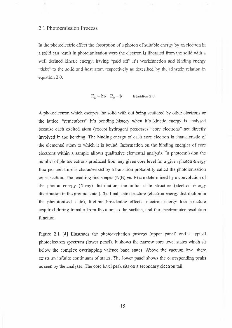
Figure 2.1 [4] illustrates the photoexcitation process (upper panel) and a typical
photoelectron spectrum (lower panel). It shows the narrow core level states which sit
below the complex overlapping valence band states. Above the vacuum level there
exists an infinite continuum of states. The lower panel shows the corresponding peaks
as seen by the analyser. The core level peak sits on a secondary electron tail.
15
When surface sensitivity is being optimised (chapter 4, section 4.6.1, figure 4.25) by
selecting a photon energy which results in a Ek value at the minimum of the Universal
curve [5], (shown in figure 2.6) the peak sits quite high on the background making
background removal (see figure 4.25) a formidable task. The contributions to the
spectrum mentioned above will be discussed next.
Figure 2.1: In the photoemission process sates below the Fermi level are probed. Above the vacuum level a continuum o f states exists. The valence band states are broad and complex; the core level states are narrow and well defined. Analysing the photoelectrons kinetic energy reveals the density o f states in the sample. The spectrum sits on a secondary electron tail [4].
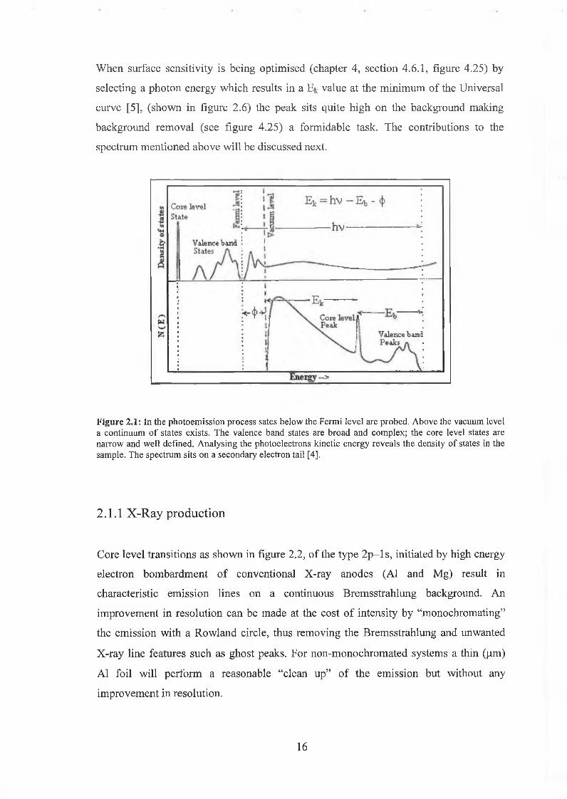
2.1.1 X-Ray production
Core level transitions as shown in figure 2.2, of the type 2p-l s, initiated by high energy
electron bombardment of conventional X-ray anodes (A1 and Mg) result in
characteristic emission lines on a continuous Bremsstrahlung background. An
improvement in resolution can be made at the cost of intensity by “monochromating”
the emission with a Rowland circle, thus removing the Bremsstrahlung and unwanted
X-ray line features such as ghost peaks. For non-monochromated systems a thin (pm)
A1 foil will perform a reasonable “clean up” of the emission but without any
improvement in resolution.
16
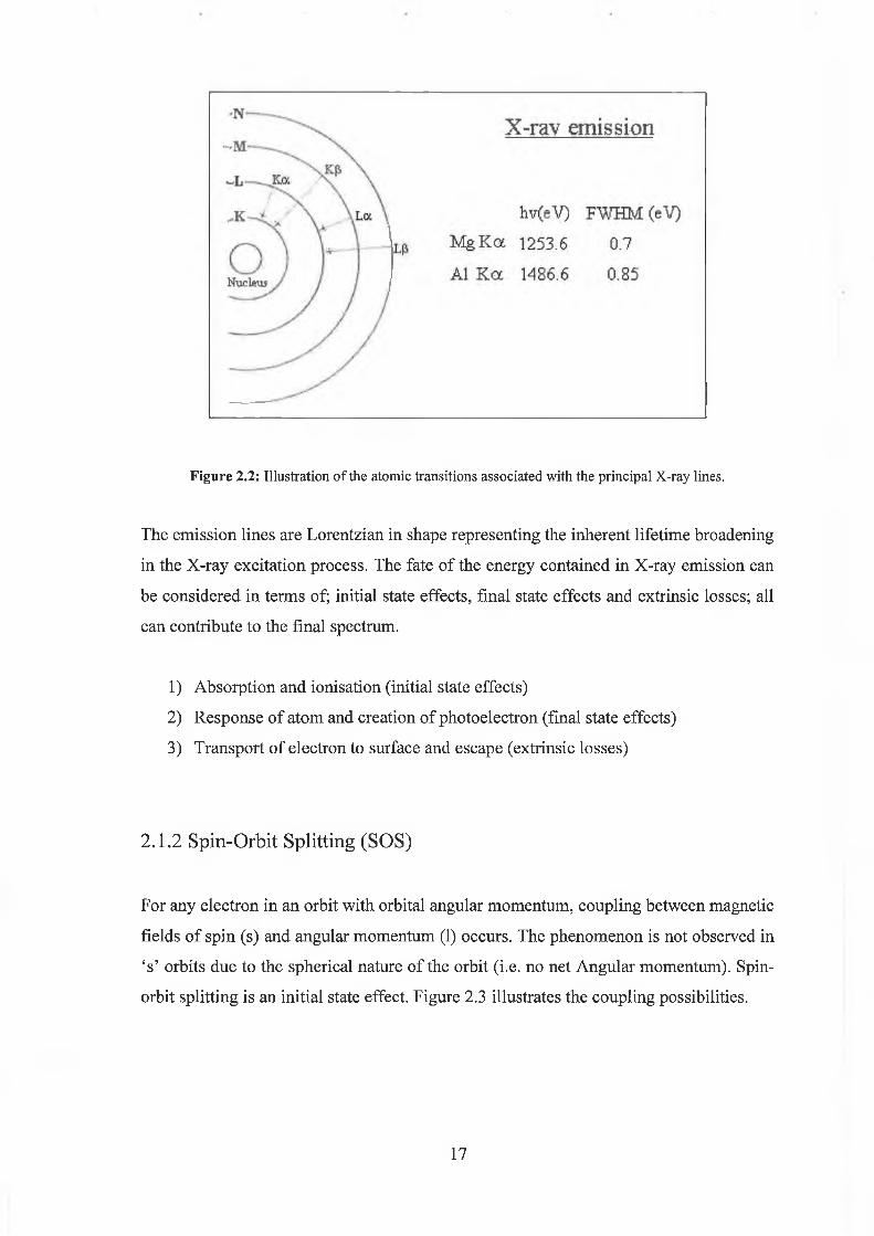
Figure 2.2: Illustration o f the atomic transitions associated with the principal X-ray lines.
The emission lines are Lorentzian in shape representing the inherent lifetime broadening
in the X-ray excitation process. The fate of the energy contained in X-ray emission can
be considered in terms of; initial state effects, final state effects and extrinsic losses; all
can contribute to the final spectrum.
1) Absorption and ionisation (initial state effects)
2) Response of atom and creation of photoelectron (final state effects)
3) Transport of electron to surface and escape (extrinsic losses)
2.1.2 Spin-Orbit Splitting (SOS)
For any electron in an orbit with orbital angular momentum, coupling between magnetic
fields of spin (s) and angular momentum (1) occurs. The phenomenon is not observed in
‘s’ orbits due to the spherical nature of the orbit (i.e. no net Angular momentum). Spin-
orbit splitting is an initial state effect. Figure 2.3 illustrates the coupling possibilities.
17
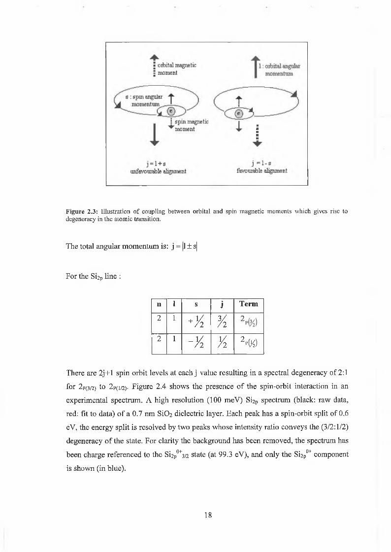
Figure 2.3: Illustration o f coupling between orbital and spin magnetic moments which gives rise to degeneracy in the atomic transition.
The total angular momentum is: j = |l ± s|
For the SÌ2P line :
n 1 s j Term
2 1+ X
3 // 2
2 1 - 1 / / 21 /72 2 -fe)
There are 2j+l spin orbit levels at each j value resulting in a spectral degeneracy of 2:1
for 2p(3/2) to 2p(i/2). Figure 2.4 shows the presence of the spin-orbit interaction in an
experimental spectrum. A high resolution (100 meV) Si2p spectrum (black: raw data,
red: fit to data) of a 0.7 nm Si02 dielectric layer. Each peak has a spin-orbit split of 0.6
eV, the energy split is resolved by two peaks whose intensity ratio conveys the (3/2:1/2)
degeneracy of the state. For clarity the background has been removed, the spectrum has
been charge referenced to the Si2P0+3/2 state (at 99.3 eV), and only the Si2P°' component
is shown (in blue).
18
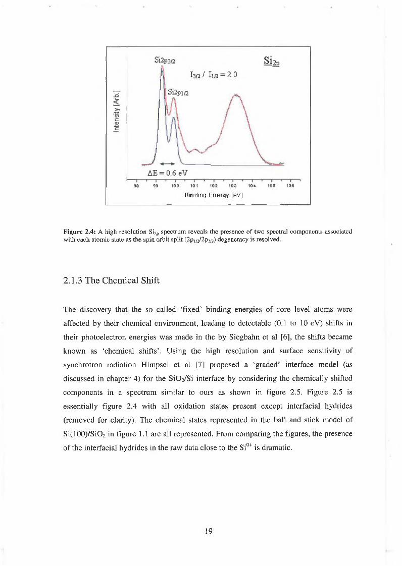
Binding E n er g y [eV]
Figure 2.4: A high resolution Si2p spectrum reveals the presence of two spectral components associated with each atomic state as the spin orbit split (2 p 1/2/2 p3/2) degeneracy is resolved.
2.1.3 The Chemical Shift
The discovery that the so called ‘fixed’ binding energies of core level atoms were
affected by their chemical environment, leading to detectable (0.1 to 10 eV) shifts in
their photoelectron energies was made in the by Siegbahn et al [6], the shifts became
known as ‘chemical shifts’. Using the high resolution and surface sensitivity of
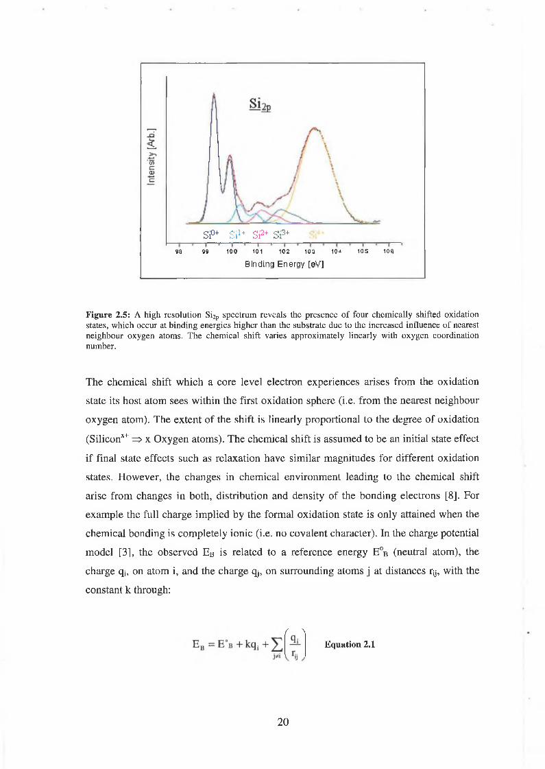
synchrotron radiation Himpsel et al [7] proposed a ‘graded’ interface model (as
discussed in chapter 4) for the S i02/Si interface by considering the chemically shifted
components in a spectrum similar to ours as shown in figure 2.5. Figure 2.5 is
essentially figure 2.4 with all oxidation states present except interfacial hydrides
(removed for clarity). The chemical states represented in the ball and stick model of
Si(100)/Si02 in figure 1.1 are all represented. From comparing the figures, the presence
of the interfacial hydrides in the raw data close to the Si0+ is dramatic.
19
Si0+ Si1+ Si2+ Si3+ga 99 100 101 102 10a 10* 10s ios
Binding Energy [eV]
Figure 2.5: A high resolution Si2p spectrum reveals the presence of four chemically shifted oxidation states, which occur at binding energies higher than the substrate due to the increased influence of nearest neighbour oxygen atoms. The chemical shift varies approximately linearly with oxygen coordination number.
The chemical shift which a core level electron experiences arises from the oxidation
state its host atom sees within the first oxidation sphere (i.e. from the nearest neighbour
oxygen atom). The extent of the shift is linearly proportional to the degree of oxidation
(Siliconx+ => x Oxygen atoms). The chemical shift is assumed to be an initial state effect
if final state effects such as relaxation have similar magnitudes for different oxidation
states. However, the changes in chemical environment leading to the chemical shift
arise from changes in both, distribution and density of the bonding electrons [8]. For
example the full charge implied by the formal oxidation state is only attained when the
chemical bonding is completely ionic (i.e. no covalent character). In the charge potential
model [3], the observed EB is related to a reference energy E°B (neutral atom), the
charge qi, on atom i, and the charge qj, on surrounding atoms j at distances ry, with the
constant k through:
/ \Equation 2.1
2 0
As the positive charge on the reference atom increases by formation of chemical bonds,
the binding energy Eb will increase. The last term in equation 2.1 (the Madelung
potential) represents the fact that the charge qi removed or added by formation of a
chemical bond is not displaced to infinity, but to surrounding atoms. Thus the chemical
shift between states 1 and 2 can be written:
EB = kAqf + AV; Equation 2.2
where AVj represents the potential change in surrounding atoms. However, the chemical
shift assignment based on charge transfer due to oxidation state is acceptable for the
S i02 system due to the well known bond length and structure, also this assignment
scheme has recently been validated by Car’s group [9] after being questioned by
Banaszak et al [10] who argued that the chemical shifts also depend on O-Si bond in the
second coordination sphere.
2.1.4 Koopmans’ Theorem [11]
The photoemission process is extremely rapid (~10‘6 sec) and the assumption that the
other electrons remain “frozen” forms the basis for Koopmans’ theorem, which states:
“The binding energy of an emitted photoelectron is simply the energy difference
between the (n-1) electron final state and the n electron initial state”.
If no relaxation follows photoemission, then the binding energy Eb is equal to the
orbital energy which can be calculated from Hartree-Fock calculations. However, other
electrons do not remain “frozen” during the photoemission process. The electron
response is discussed in section 2.1.7. Despite this, the spectral implications of electron
relaxation processes can be catered for during peak fitting and so Koopmans’ theorem
provides a working basis.
21
2.1.5 Surface Sensitivity
The penetration depth of X-rays in solids is on of order of several microns due to the
low interaction between photons and the material. However, whether or not a
photoelectron excited at a certain depth will pass through a solid without scattering after
absorbing an X-ray depends on it’s kinetic energy and the nature of the material. The
average distance an electron with a given energy travels between inelastic collisions is
known as the Inelastic Mean Free path (IMFP), whose functional relationship for the
elements is described by Seah and Dench [12]:
IMFP = X = 538— j + 0.41^/aEk Equation 2.3E k
A, is in units of monolayers
a monolayer thickness (nm)
Ek electron kinetic energy (eV)
Therefore photoelectrons with kinetic energies in the 10-1000 eV energy range, above
the Fermi energy, must originate very close (<10 nm) to the surface in order to emerge
unscattered and make up the primary photoelectron peak. Inelastically scattered
electrons contribute to the secondary electron background. Herein lies the surface
sensitivity of photoemission. In synchrotron studies the minimum in the ‘universal’
curve shown in figure 2.6 (IMFP vs. Ek) is exploited when an incident photon with a
given energy results in photoelectrons emerging exclusively from the outermost atomic
layers due to the strong interaction of low kinetic energy electrons with the sample.
Also by considering off angle emission (grazing incidence), the longer path to be
travelled by grazing photoelectrons deep in the solid means they are attenuated more,
and so the primary peak arises from surface photoelectrons.
22

Figure 2.6: The universal trend for a minimum in the IMFP o f photoelectrons with a kinetic energy of approximately 50 eV is mapped out by the universal curve [5],
2.1.6 Final state effects
During the photoemission process, other electrons in the sample respond to the creation
of a core hole by rearranging to shield, or minimize, the energy of the ionised atom.
Relaxation of electrons from the atom containing the core hole is known as atomic
relaxation and from electrons on surrounding atoms as extra-atomic relaxation. Most of
the atomic relaxation component is due to the rearrangement of outer shell electrons,
which have a smaller Eb than the photoelectron. The inner shell electrons who’s Eb is
larger than the emitted photoelectron, have a small contribution and are neglected. The
form of extra-atomic relaxation depends on the material being examined. In metals and
highly doped semiconductors, valence band electrons can move from one atom to the
next to screen a core hole.
2.1.7 Peak broadening
Ultimately a core level photoelectron signal presents itself as a Voigt peak on a
secondary electron background. A core level Voigt peak is a convolution of a
Lorentzian and a Gaussian peak. It’s FWHM contains contributions from; the X-ray
source ES0Urce, the electron analyser Eanaiyser, and energy uncertainty due to the core hole
23

lifetime E|,oie. The sum of the square of these factors is the square of the measured
FWHM:
(AEM f = (A E ,„ f + ( a E , .^ , J2 + (AEU, f Equation 2.4
The line shape due to the lifetime of the core hole is Lorentzian. Lifetime broadening
results in symmetric broadening. Lifetime broadening can be gauged from the
Heisenberg uncertainty principle
, h1 = — Equation 2.5
X
r is the intrinsic peak width in eV
h Planck’s constant in eV seconds
x is the core hole lifetime in seconds
A typical value of T is 0.1 eV. The instrumental broadening of the X-ray source and
analyser is Gaussian. For non-metallic samples broadening also arises from charging.
Asymmetric broadening can occur in metals and highly doped semiconductors where
the production of a positive potential site with a final state energy lower than the
original surface scatters conduction electrons across the Fermi level, providing a
continuous range of allowed one-electron excitation energies, resulting in a asymmetric
tailing of the main peak to the high binding energy side, the extent of which depends on
the density of states at the Fermi level.
Plasmon losses'.
A plasmon peak arises from a collective oscillation of a group of charges or Plasma (i.e.
free electrons in a metal or gas). A photoelectron passing through a crystal couples with
its longitudinal electric field and electron density fluctuations to create extrinsic
plasmons. Intrinsic plasmons are produced during core-hole relaxation. Following the
photoelectric excitation of bound electrons, plasmons show up as broad smooth replicas
of the photoelectron peaks shifted to lower kinetic energy by an amount equal to the
24
plasmon energy C0ph/27t. In the free electron approximation, the plasmon energy is
related to the valence electron density as
VWp 271 y V27Iy_1_mît
N v Equation 2.6/
C0ph/27i is the plasmon energy
m is the electron mass
q is the electron charge
Nv is the valence electron density
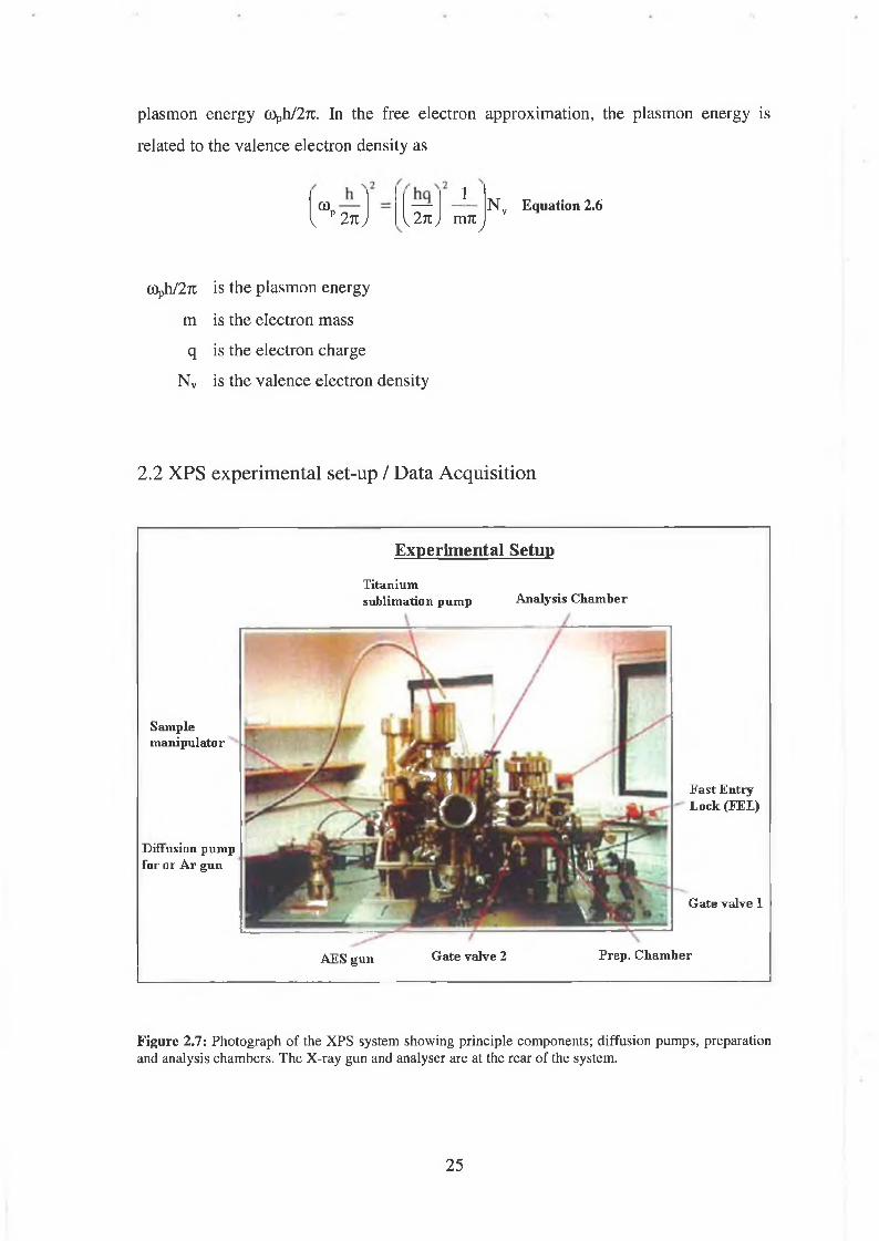
2.2 XPS experimental set-up / Data Acquisition
Experimental Setup
Titaniumsublimation pump Analysis Chamber
Samplemanipulator
Diffusion pump for or Ar gun
AES gun Gate valve 2
Fast Entry Lock (FEL)
Gate valve 1
Prep. Chamber
Figure 2.7: Photograph of the XPS system showing principle components; diffusion pumps, preparation and analysis chambers. The X-ray gun and analyser are at the rear of the system.
25
Figure 2.7 shows a photograph of the XPS system. It is equipped with two rotary
backed diffusion pumps, which maintain UHV pressures in both the analysis and
preparation chambers. An additional fast entry lock (FEL) chamber allows samples to
be introduced from air to UHV quickly. The pressure in the preparation and analysis
chamber are isolated from each other and from the FEL via UHV compatible gate
valves. Samples are transferred using a trolley system and wobble sticks. The analysis
chamber is equipped with a VG clam analyser with electrostatic lens, an Auger electron
spectroscopy gun and a differentially pumped ion sputter gun. The X-ray gun is (Mg/Al)
twin anode. The system is equipped with a titanium sublimation pump.
Pump down
When the vacuum is “broken” to either repair or replace parts on the system it is vented
with nitrogen in order to protect the clean internal walls from excess ambient
contamination. From atmospheric pressure UHV is achieved by “roughening” out the
system using rotary pumps. The diffusion pumps are used in order to achieve high
vacuum (~10‘5 mbar). However, unavoidable contamination on the inside walls due to
loss of vacuum acts as a constant source of pressure and so the system is “baked” at 120
°C for approximately 12 hours allowing the contamination to desorb from the vessel
walls. After degassing cycles and allowing the system to cool to room temperature a
pressure of approximately 4x1 O'10 mbar is achieved in which an atomically clean
surface can be maintained for a reasonable amount of time and a photoelectron signal
can traverse macroscopic distances without interacting with other atoms outside the
sample being examined.
Analyser
Under the control o f a computer the photoelectron flux from the surface is collected
through a focusing electrostatic lens where the kinetic energy is interrogated by a
hemispherical analyser. The tiny photoelectron current (~nA) is then amplified by a
channeltron and undergoes analogue to digital conversion were it is finally presented by
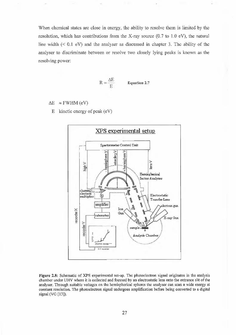
the computer as a digital spectrum as shown in figure 2.8 [13]. In XPS the chemical
bonding states in the sample are revealed through the chemical shifts of core level
peaks.
26
When chemical states are close in energy, the ability to resolve them is limited by the
resolution, which has contributions from the X-ray source (0.7 to 1.0 eV), the natural
line width (< 0.1 eV) and the analyser as discussed in chapter 3. The ability of the
analyser to discriminate between or resolve two closely lying peaks is known as the
resolving power:
T, AEK. = Equation 2.7
AE « FWHM (eV)
E kinetic energy of peak (eV)
channel t -, electron multiplier >
,electron gun
ratemeter
Analysis Chamber
Spectrometer Control Unit
> . > >0) cn <D53«—
c o3"D Jc
% 1£
JDû)
t\ Hemispherical
\ Sector A nalyzer
Electrostatic Transfer Lens
♦lector i w w —
XPS experimental setup
Figure 2.8: Schematic o f XPS experimental set-up. The photoelectron signal originates in the analysis chamber under UHV where it is collected and focused by an electrostatic lens onto the entrance slit o f the analyser. Through suitable voltages on the hemispherical spheres the analyser can scan a wide energy at constant resolution. The photoelectron signal undergoes amplification before being converted to a digital signal (VG [13]).
27

For a large energy window as in figure 2.10, the resolving power changes with kinetic
energy. In order to analyse all kinetic energies with the same resolution the incident
photoelectrons are pre-retarded to a constant pass-energy Ep. Photoelectrons entering
on-axis at the input slit of the hemispherical analyser are deflected by an electric field
between the two hemispheres in such a way that only those electrons travelling at the
pass energy Ep of the analyser follow the path of the mean radius Ro and arrive at the
exit slit for amplification. Figure 2.9 [14] shows a cross-section of the CHA.
Hemispherical Sector Analyser
width width
Figure 2.9: Cross-section o f a CHA analyser. Photoelcctrons entering on-axis at the input slit of the hemispherical analyser are deflected by an electric field between the two hemispheres in such a way that only those electrons travelling at the pass energy Ep o f the analyser follow the path o f the mean radius Ro and arrive at the exit slit for amplification [14].
Two hemispheres of radii Ri (inner) and R2 (outer) have negative potential of Vi and V2
applied to them respectively, where (V2>Vi). The potential along the mean path Vo is
given by:
V RV0 = VjR, + —- —— E quation 2.8
2R0
28
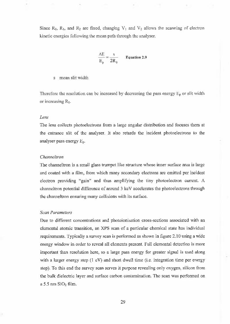
Since Ro, Ri, and R2 are fixed, changing Vi and V2 allows the scanning of electron
kinetic energies following the mean path through the analyser.
AE s ------= -------- Equation 2.9Ep 2R0
s mean slit width
Therefore the resolution can be increased by decreasing the pass energy Ep or slit width
or increasing Ro.
Lens
The lens collects photoelectrons from a large angular distribution and focuses them at
the entrance slit of the analyser. It also retards the incident photoelectrons to the
analyser pass energy Ep.
Channeltron
The channeltron is a small glass trumpet like structure whose inner surface area is large
and coated with a film, from which many secondary electrons are emitted per incident
electron providing “gain” and thus amplifying the tiny photoelectron current. A
channeltron potential difference of around 3 keV accelerates the photoelectrons through
the channeltron ensuring many collisions with its surface.
Scan Parameters
Due to different concentrations and photoionisation cross-sections associated with an
elemental atomic transition, an XPS scan of a particular chemical state has individual
requirements. Typically a survey scan is performed as shown in figure 2.10 using a wide
energy window in order to reveal all elements present. Full elemental detection is more
important than resolution here, so a large pass energy for greater signal is used along
with a larger energy step (1 eV) and short dwell time (i.e. integration time per energy
step). To this end the survey scan serves it purpose revealing only oxygen, silicon from
the bulk dielectric layer and surface carbon contamination. The scan was performed on
a 5.5 nm S i02 film.
29
I

Despite the larger oxygen concentration relative to silicon (0:Si 2:1), the higher
photoionisation cross-section of oxygen results in its substantially larger intensity.
Silicon is represented by two transitions, namely the Si2S and Si2P. The smaller
photoionisation cross-section of the Si2S state and its relatively smaller bonding
interaction makes the Si2P state the preferred transition to investigate for bonding
information. High-resolution scans were performed on the Si2P, Ois, and Cjs peaks. Here
resolution is important in order to elucidate as best as possible chemical shifts on the
primary peaks and so a pass energy of 20 eV, an energy step of 0.1 eV, and a dwell time
of 0.25 sec are typical scan parameters. Figure 2.11 shows a high-resolution scan of the
Si2P peak shown in figure 2.10. The Si0+ substrate peak and chemically shifted (4 eV to
lower kinetic energy) Si4+ oxide peak are clearly resolved. However, the spin orbit
splitting (0.6 eV) on the substrate peak is not resolvable given that the experimental
resolution achievable with the XPS instrument is approximately 1 eV.
Kinetic energy [eV]
Figure 2.10: A wide energy “survey” scan reveals all elements present allowing a suitable energy window to be decided for subsequent higher resolution scans.
From the previous discussion of the operation of the analyser it is tempting to seek
better resolution by decreasing the pass energy Ep of the analyser. However, as is often
the case in optics there is a fundamental trade-off between resolution and intensity.
When the slit width is very small, at small pass energies, the analysed photoelectron
30
flux is small and the signal to noise is dramatically affected. Some improvement can be
found by dwelling for longer at each kinetic energy sampling step in the scan. Because
the spectrum is a digital signal, which has been sampled with a finite resolution, it
would be ambiguous to infer spectral structure beyond that resolution. Although it is
acceptable to sample the signal with an energy step of say 0.1 eV, it is not acceptable to
attempt to resolve with certainty spectral features beyond 1 eV. Despite this restriction
spectra are typically de-convoluted beyond the available resolution based on a prior
knowledge or expectation of the exact chemical state from say high-resolution
synchrotron analysis.
2.3 Data Analysis
Under the control o f a P.C. the analyser interrogates the kinetic energy of the incident
photoelectron flux. The tiny photoelectron current (~nA) is then amplified by a
channeltron and undergoes analogue to digital conversion were it is finally presented by
the P.C. as a digital spectrum. Before peak de-convolution can be performed the
background on which the spectrum sits needs to be identified and removed.
Background type / removal
Photoelectron peaks are found on a “stepped” background, which has contributions
from:
• The Bremsstrahlung of the X-ray source and the tails of neighbouring peaks.
This can be removed with a constant baseline fitted to the high kinetic energy
side of the spectrum.
• Extrinsic losses from inelastic scattering events during electron transport
through the solid. These losses have been study by Tougaard [15] and can
removed by a Tougaard background.
• Intrinsic satellite losses inherent to the photoexcitation process in the atom and
associated with it's nearest neighbours, and includes valence electron excitations
31
(shake-up) and excitation of vibrational motion, plasmon excitations, and
interband transitions [16].
Background removal is complicated as both intrinsic and extrinsic contributions span
similar energies and the peak intensity will depend on the method used to remove the
background. For the samples studied in this thesis, intrinsic losses are of concern for the
Si0+ when the substrate is highly doped and takes on metallic behaviour. The
backgrounds obtained during synchrotron studies show a small stepped character and
are best fitted with a Shirley [17] or Tougaard algorithm. For conventional XPS, a 4th
order polynomial is used to fit the background. The polynomial is defined as:
P(X) = x „ + X, ( x - x p ) + x 2 (x - X p )J + JTj ( x - X p ) + X , ( x - X p )*
E quation 2.10
Xp is an offset on the x-axis
Xi is the ith coefficient of the polynomial
Gausstsn 9D %
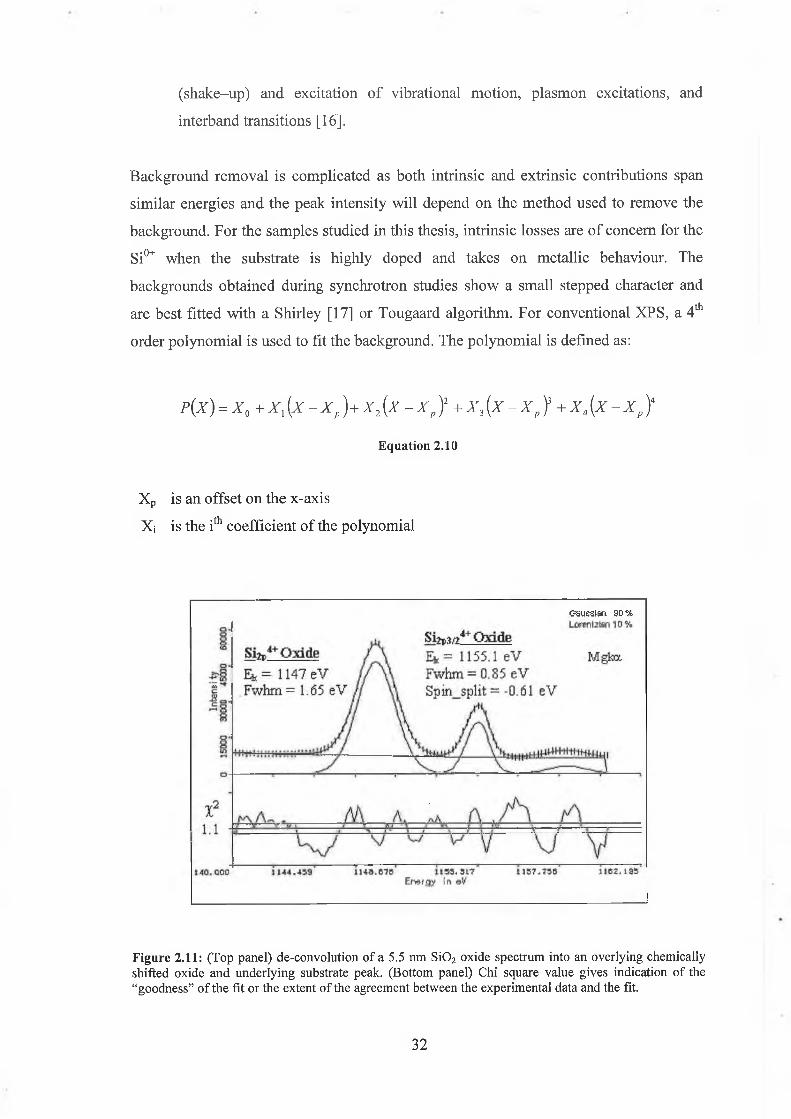
Figure 2.11: (Top panel) de-convolution of a 5.5 nm S i0 2 oxide spectrum into an overlying chemically shifted oxide and underlying substrate peak. (Bottom panel) Chi square value gives indication o f the “goodness” o f the fit or the extent o f the agreement between the experimental data and the fit.
32
Figure 2.11 shows a fit to the SÌ2P spectrum of a 5.5 nm oxide. The spectrumthbackground was fitted using a 4 order polynomial. Here the polynomial background
easily fits what is essentially a linear background, as checked by numerical
differentiation of the fitted background. An initial guess for the background, peak
intensity, kinetic energy, and FWHM were made.
Peak parameters
The spectrum was fitted with two Voigt peaks, as defined by equation 2.11, a linear
combination of a Gaussian G(x), and a Lorentzian L(x) peak in order to express the
influence, respectively, of the instrumental broadening of the energy distribution of the
photoexcited orbital and the core-hole lifetime.
M(x) = aG(x)+ (l - a)L(x) Equation 2.11
Where G(x) (the Gaussian ) and L(x) (the Lorentzian) are curves with the same position
and width. Because the peak is predominantly Gaussian the mixing parameter ‘a’ is 0.9,
(i.e. 90% Gaussian and 10% Lorentzian).
The Gaussian is defined by:
G (x)=h i_ ?4 In 2
x - x 0w
Equation 2.12
h is the peak intensity
xo is the position of the peak
w FWHM
The Lorentzian is defined by:
L(x ) = Equation 2.13
1 + 4 x - x 0w
33

h is the peak intensity
xo is the position of the peak
w FWHM
Values for spin-orbit splitting of -0.6 eV and an intensity ratio of 0.5 are well
established in the literature [7],[22],[49] and confirmed by our own synchrotron studies
of clean silicon. They are held constant during fitting. Once started, the fitting program,
through an iterative least squares fitting cycle seeks to reduce the chi-square x2 value
[18] (sum of the squares of the deviations), which indicates the goodness of fit between
the experimental and guessed peaks. In general, a smaller %2 value represents a better fit;
with values less than 1 indicating that the fit and the data are indistinguishable within
the experimental error. The bottom part of figure 2.11 shows the residues, the difference
between the fitted and experimental data. The inability to detect interfacial suboxides is
apparent by the goodness of fit across the energy window. The interfacial signal is small
and attenuated by the overlying bulk. When a peak is required and has not been
included in the fit the localized disagreement in the residue is a useful warning or
indication of its absence.
2.4 Quantification [19]
In a simplistic view the intensity of a given elemental photoelectron peak can be
interpreted in terms of the concentration of that element in the sample and the outgoing
photoelectron signal suffering a simple Beer Lambert like attenuation with depth as
shown in figure 2.12. It is only through careful spectral analysis involving background
removal, peak de-convolution and taking instrumental factors into consideration that the
percentage of each element detected can be calculated. Figure 2.12 [19] shows a
simplified but useful representation of the attenuation of the photoelectron flux by the
solid and overlayer when “deeply” (|J.m) penetrating X-rays are considered as
stimulating photoemission throughout the bulk of the sample.
34
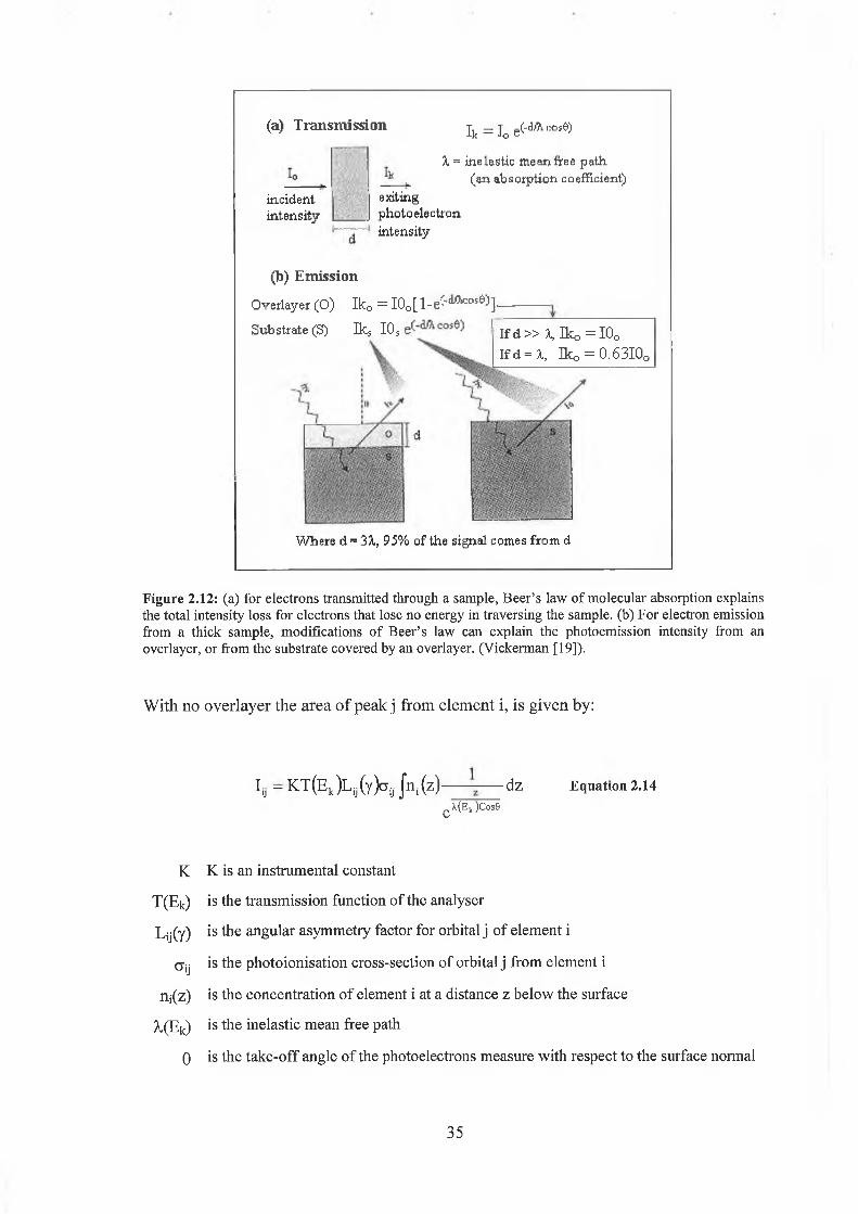
(b) Emission
Overlayer (O) Iko = I0 „ [ 1 - e ^ 05^ ] -
Sub strate (S) Ik* IQS If d » X, Iko = I0o I f d = S., Iko = 0.63I0o
W here d= 3X, 95% of the signal comes from d
(a) Transmission
incidentintensity
X = inelastic mean free path (an absorption coefficient)
Ik = ]0 ei-dA<:os
exitingphoto electron intensity
Figure 2.12: (a) for electrons transmitted through a sample, Beer’s law o f molecular absorption explains the total intensity loss for electrons that lose no energy in traversing the sample, (b) For electron emission from a thick sample, modifications o f Beer’s law can explain the photoemission intensity from an overlayer, or from the substrate covered by an overlayer. (Vickerman [19]).
With no overlayer the area of peak j from element i, is given by:
ly - KT(Ek)Lij(y)aij Jn. (z) - dz Equation 2.14e ^ ( E k )Cos0
K K is an instrumental constant
T(Ek) is the transmission function of the analyser
Lij(y) is the angular asymmetry factor for orbital j of element i
<*ij is the photoionisation cross-section of orbital j from element i
ni(z) is the concentration of element i at a distance z below the surface
MEk) is the inelastic mean free path
0 is the take-off angle of the photoelectrons measure with respect to the surface normal
35
The instrumental constant K expresses the X-ray flux, area of sample irradiated, and
solid angle of photoelectrons accepted by the analyser. The angular asymmetry accounts
for the type of orbital the photoelectron is emitted from and the angle y between the
incident X-rays and emitted photoelectrons. The transmission function of the analyser
includes the efficiency of the collection lens, the electron analyser and detector. The
analyser was operated in fixed analyser transmission mode, by pre-retarding the
incoming electrons to a constant pass energy in order to maintain constant energy
resolution across the scan. The photoelectron ionisation cross-section cry is the
probability that the incident X-ray will create a photoelectron from the j orbital of
element i. The values calculated by Scofield [20] were used and also values were
calculated using quantification (Polymer) samples as discussed later.
2.4.1 Si02 Overlayer Model
A thin (d<3A,) SiCh film on an infinite Si substrate attenuates the photoelectron flux
passing through it (see figure 2.12 (b)). Using equation 2.14 the intensities from the
overlayer and substrate intensities are given by:
Emission from the substrate is attenuated by the overlayer and is thus multiplied by
dz Equation 2.15
I Sj = K T ( E k)L si(Y)tfsi^si 1 --------- — E quation 2.16
3— to give:^Si02 Cos0
V
/ A
I si = K T ( E k)L ij(y ) a ijXSio2 l— E quation 2.17_ A,e;CoS0\

By consider the ratio of the intensities of the oxide to substrate peak the K and analyser
transmission terms are common and cancel. The orbital angular asymmetry terms are
neglected, as their correction is small. A number of assumptions which are reasonable
for amorphous S i02 in the ultra-thin regime (<5 nm) are employed;
• Elastic scattering in the sample is neglected
• Electron diffraction effects are negligible
• The IMFP is independent of depth (the film is stoichiometric S i02)
• Reflection and refraction of X-rays is negligible
• The IMFP of S i02 and Si are approximately equal
• Angular asymmetry is neglected
• Surface roughness is negligible
This allows us to write:
Isi02 _ I oo SiC>2 -1 E quation 2.18
where Iro = nsi02a si0jx,sj0j & I0 = nSla SjXSi are the intensities for an infinitely thick Si02
layer and bare Si substrate, respectively. Values for 1«, / Io and X si02 are taken from
Himpsel et al [7]. Rearranging equation 2.18 allows the thickness of the overlaying
oxide to be calculated:
d = Ln Isio2 Ip
Is. I .+1 '"SiO, E quation 2.19
2.4.2 Oxide Stoichiometry
The relative concentration of atom ‘i’ in an infinitely thick homogeneous sample can be
calculated from the total intensity from:
37
N ¡ = E quation 2.20
F| = C J jL ^ j, pj ^ ¡ T ; Equation 2.21
aj : atomic sensitivity factor based on Scofield’s [20] photoionization cross sections.
471-C o s 2 2V \
: orbital angular asymmetry correction where |3,
is the asymmetry term and cp is the angle between the excitation source and the analyser.
The actual values for the IMFP of photoelectrons in matter are a function of the energy
of the electrons and the nature of the sample through which they travel. For typical XPS
energies the IMFP increases with electron kinetic energy. The Ek dependency of the
inelastic mean free path can be accounted for through an exponential dependence Aj oc
Ea (0.5<a<0.9), 0.7 is typically used [21]. Equations that relate the IMFP to the electron
energy and type of material (elements, organic materials or polymers) through which
the electron travels have been developed by Seah and Dench [12].
Tj: as mentioned above is the transmission function of the analyser which includes the
efficiency of the collection lens, the electron analyser, and detector. In this thesis work
the analyser was operated in FAT mode, by pre-retarding the incoming electrons to a
constant pass energy in order to maintain constant energy resolution across the scan.
Thus the only variation in the transmission function with Ek of the photoelectrons was
due to the retardation of the lens system.
Only the atomic sensitivity factor a, in equation 2.21 is considered in quantitative
analysis. The orbital asymmetry term is small and the sample composition and analyser
transmission function are common to each scan. The applied quantification of equation
2.20 gives relative concentrations thus the results should be normalised. It is usual to
consider either the atomic percentage of element ‘i’ as in:
R. = N.-100
i —ii
I N ,E quation 2.22
, i=0
38

Ni is the relative concentration of element ‘i ’ from equation 2.20
Ri is the normalised relative concentration
Thus the atomic percentage of Si in the dielectric layer can be calculated using the Si2P4+
oxide and Ois peak intensities:
(%Si) = SiO ;/ I I N
XSiQ2 | Q l
SiO, As /
Equation 2.23
similarly for oxygen:
(%o)=l S i0 2 +a SiO 2 Is /
Equation 2.24
Isioa Si2p Oxide photoelectron peak intensity
Io,. Ois Oxygen photoelectron peak intensity
c atomic sensitivity factor based on Scofield’s [20] photoionization cross
sections
2.4.3 Quantification standard
In order to verify our values for O and Si sensitivity factors a standard polymer material
was analysed. A thin film of polydimethysiloxane (PDMS) was allowed to flow over a
thin silver foil. This polymer has a known elemental composition (except hydrogen) of
25% Si, 25% O and 50% C. Because of it’s low surface energy the polymer can be
prepared ex-situ with negligible adsorption of hydrocarbons, water and C 02 that
generally eliminate organic materials as standards [22].
39

Figure 2.13 shows a wide survey scan of the principal peaks; Ois, Cis and Si2P of a thin
PDMS film.
Polydimethysiloxane (PDMSA)
Kinetic Energy [eV]
Figure 2.13: A wide survey scan o f a thin PDMS film showing the principal peaks. The film has a known elemental composition o f oxygen, carbon and silicon in percentages o f 25%, 50% and 25% respectively.
In this scan all peaks are on the same absolute intensity scale and despite having twice
the concentration of oxygen and being distributed uniformly through the film, it is
apparent that the intensity of the carbon peak is not twice that of the oxygen peak, this is
due to it’s different photoionisation cross-section or sensitivity factor. From the known
elemental composition of the PDMS film and using the intensities of the Ois, Cs and Si2P
photoelectron peaks along with equation 2.22; values of sensitivity factors for O and Si
can be calculated. Relative sensitivity factors for O and Si are obtained as there are three
equations with three unknowns and so for a solution the sensitivity factor for carbon is
set equal to 1.
Setting ct cis= l-0 and solving for a si2P and a ois gives:
40
(%Si) = a si,„
!‘2P | 10
’>2p Ol5
In
Is _j HsOr Is /
( % 0) ='o,s
( ISio Siv 51 ip 'Oi, f r '-In
F igure 2.14: Silicon, carbon and oxygen photoelectron signals from a quantification standard (PMDS) for oxidised species.
Figure 2.14 shows high resolution scans of the oxygen carbon and silicon photoelectron
peaks from the film.41
In the wide survey scan of an as-received SiC>2 film in figure 2.10 a small carbon peak is
evident and is associated with hydrocarbon contamination. Hydrocarbon contamination
is unavoidable when analysing a sample, which has been exposed to the laboratory
atmosphere. The SiC>2 dielectric layer is water insoluble, chemically inert and so
adsorption of hydrocarbons, water, CO2 etc., exists in thickness in the order of a couple
of monolayers. This hydrocarbon layer undermines quantitative analysis as it attenuates
the photoelectron from the sample underneath it [23] (as discussed in chapter 3). The
contamination layer is particular problematic in angular resolved experiments at high
take-off angles where an outgoing photoelectron travels through an effectively thicker
contamination layer because of the grazing emission angle. Hofmann et al [24]
proposed a graphical method to remove the contamination effects from the value of
stoichiometry. It assumes that the contamination layer thickness is one monolayer. Also
in the model the contamination thickness can vary to less than an atomic diameter and
the contamination layer is small relative to the escape depth for carbon in a carbon
matrix. Hofmann checked his model with samples, which had undergone in-situ ozone
cleaning, O2 discharge cleaning and different degrees of ambient hydrocarbon
contamination. The algorithm is computationally difficult to implement. Contamination
could also be accounted for by including in equation 2.21 a surface contamination
correction term e"c/x as proposed by Evans et al [25] to give equation 2.25 below:
F; = a jL((pi , (3; )X t \ E quation 2.25
e*-
In this thesis work carbon contamination is a cause for concern primarily for the as-
received samples where it is consistently small, given the precision which the
environment in which the oxides were grown and stored. Assuming that surface
contamination does not evolve with time or sampling processing; inter sample
comparisons where peak intensity ratios (i.e. Ois/Si2P4+) are considered will result in
such effect being cancelled. This approach is motivated by the belief that an objective
and non-ambiguous characterisation procedure for the oxide layer using XPS should
2.4.4 Hydrocarbon Contamination
42
consider the evolution of as-received parameters (thickness, stoichiometry, chemical
shift) in an inter as-received comparison as opposed to the calculation of absolute values
of thickness, stoichiometry or chemical shift.
2.4.5 Oxide Charging
Charging effects arise from the inability of an insulator to respond to the depletion of
photoelectrons due to X-ray illumination. In the S i02/Si system a core hole created in
the silicon substrate can be quickly filled due to the moderate doping and good electrical
contact with the spectrometer. In the oxide a core hole exists for a longer time due to the
deficiency of mobile charge. The positive charging of the oxide layer causes the entire
photoelectron spectrum to “charge” or shift to higher binding (lower kinetic) energy.
Illuminating the sample with a flux of low energy electrons (< 5 eV) replaces the
depleted photoelectrons. Because all peaks are shifted to the same extent, charge
correction can be performed by referencing to the known substrate or surface
contamination binding energy. The substrate is doped and is in electrical contact with
the spectrometer, which is grounded and so cannot be depleted. For thick dielectric
layers where the substrate peak signal cannot be “seen” through the oxide overlayer
charge referencing was performed using the binding energy of adventitious hydrocarbon
adsorption at 285.6 eV.
Charge referencing using the silicon substrate peak (Si0+) [26,27] or Fermi edge is
undermined by their variation with dopant type and concentration. The use of C-C peaks
[28] is hindered by differential charging. In a round robin experiment by Hashimoto et
al [29], charge correction in oxides using the hydrocarbon Cis binding energy resulted in
errors as large of 11 eV. The Cis line for adventitious contamination is between 283.8
and 285.6 eV. The study concluded the best results would be obtained by referencing
using the energy difference between the Ois and Si2p4+ oxide peak (i.e.: E b o i s -
E b s i 0 2 = 4 2 9 . 3 eV) having chosen a value of for the oxide binding energy (E b s i 02= 103.0
eV). In this approach a chemical shift would result in a change in the oxygen to oxide
energy difference but a charging shift would result in a constant separation. Because of
the consistency and precision with which the dielectric layers studied in this thesis were
43
prepared (i.e. doping), charge correction was performed by referencing to the Si2P0+
substrate peak binding energy at 99.3 eV and for infinitely thick oxides using the Cis
binding energy at 285.6 eV. As with stoichiometry it is potentially more useful to be
concerned about the consistency in peak positions as opposed to elucidating absolute
binding energies.
Image charge
In very thin (d<2 nm) dielectric layers a thickness dependent chemical shift is evident
where electrons ejected from the Si atoms in the SiC>2 layer have a reduced binding
energy due to the coulomb interaction with the core hole (positive ion) because they
also feel the screening (repulsion) of its image charge in the substrate.
2.5 S i02 Chemical Depth profiling
XPS is effectively a chemical “flash torch” where high energy photons penetrate
micrometers into the sample, however due to the strong interaction of electrons with
matter, chemical state information is only “illuminated” within the sampling depth (3 A,),
giving rise to XPSs surface sensitivity. XPSs wide energy window (1486 eV) and large
sampling depth (3A.si02~l 0 nm) allows the quality of the overlying oxide in a SiCVSi
layer to be ascertained from the consistency of the oxide elemental composition,
bonding and thickness. Limited resolution, surface sensitivity and a desire to illuminate
the Si/Si02 interface have motivated researchers to depth profile the film for better
interfacial sensitivity. Profiling through the oxide layer has been performed using Ar+
ion bombardment. It offers a reasonable removal rate across large areas, but is believed
to preferentially remove oxygen in Si02 leaving a reduced and damaged outer surface, it
also introduces lattice damage by re-ordering the inter-tetrahedral Si-O-Si bond angle
resulting in an increase in Si2P4+ oxide peak FWHM. The introduction of surface
suboxides by ion bombardment, which cannot be distinguished from interfacial
suboxides, would seriously undermine any attempt to probe the interface. Increased
surface sensitivity has been achieved in angular resolved studies, where the chemical
depth profile is reconstructed from the individual spectra considered at different take-off
angles. The reconstruction is performed through an iterative optimisation algorithm
44
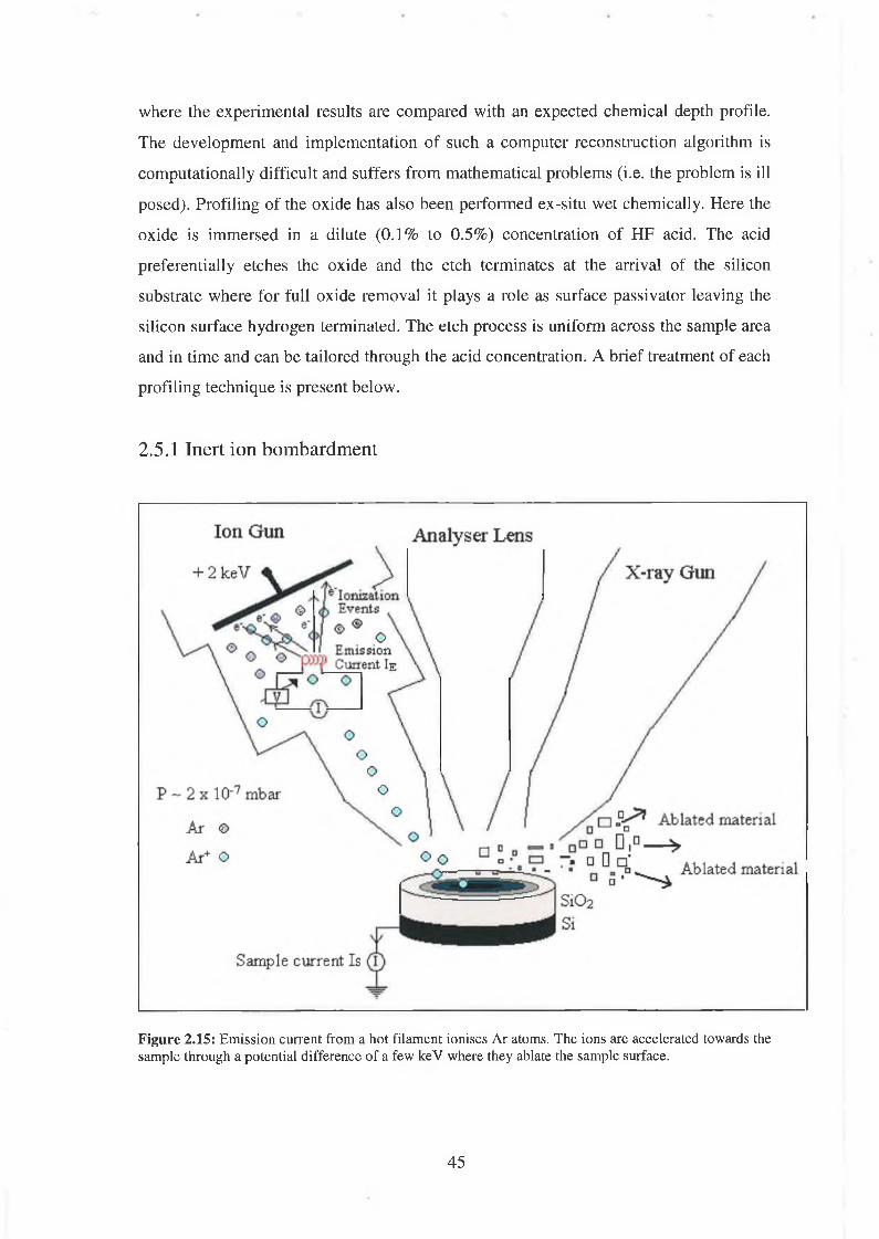
where the experimental results are compared with an expected chemical depth profile.
The development and implementation of such a computer reconstruction algorithm is
computationally difficult and suffers from mathematical problems (i.e. the problem is ill
posed). Profiling of the oxide has also been performed ex-situ wet chemically. Here the
oxide is immersed in a dilute (0.1% to 0.5%) concentration of HF acid. The acid
preferentially etches the oxide and the etch terminates at the arrival of the silicon
substrate where for full oxide removal it plays a role as surface passivator leaving the
silicon surface hydrogen terminated. The etch process is uniform across the sample area
and in time and can be tailored through the acid concentration. A brief treatment of each
profiling technique is present below.
2.5.1 Inert ion bombardment
F igure 2.15: Emission current from a hot filament ionises Ar atoms. The ions are accelerated towards the sample through a potential difference of a few keV where they ablate the sample surface.
45

Figure 2.15 shows a typical XPS experimental set-up where due to the need to collect as
much signal as possible the sample is usually in close proximity to the X-ray source,
analyser lens and ion gun. In order to bombard the sample the chamber is back filled
with argon to a pressure of approximately 2-5 x 10'7 mbar. The argon line is
differentially pumped to maintain a constant flux of argon. A hot filament in the gun
acts as a source of energetic thermionic electrons which discharges through a positive
plate to give an emission current. This emission current can ionise the Ar atoms, which
make up the background pressure. Once ionised, the Ar+ ion can be accelerated towards
the sample under the influence of the potential difference between the positive plate and
the sample, which is grounded. The ions crash into the sample where their momentum
and thermal energy is used to remove or ablate the outer surface of the sample. The rate
of sample removal can be regulated through the accelerating potential difference, the
background pressure of argon and the focusing of the ion beam. In profiling the oxide
the gun was operated with the beam defocused in order to achieve uniform ablation. Ion
bombardment is realised through a plasma discharge of ions which is inherently
unstable and typically the removal rate is not uniform in time or spatially with a crater
being formed in the centre of the sample which can lead to “shadowing” effects in off-
angle analysis where the oxide signal is enhanced at the detriment of the substrate signal
due to the crater realised during bombardment.
Figure 2.16 is a simplified illustration of the process. The ability to profile the sample
in-situ thus avoiding re-exposure to the laboratory ambient using Ar ion bombardment
is advantageous. Reproducibility and consistency in rate of oxide removal coupled with
shadowing effects and ultimately the reduction of the outer surface region during
bombardment (surface reduction is discussed at length in chapter 3, section 3.3) makes
the technique unsuitable. When complete oxide removal was necessary and surface
damage could be repaired through annealing as with germanium samples (chapter 6),
where Ar ion bombardment proved very useful.
46

Shadowing Effects
Analyser x _ray Gun Analyser x . ray Gun
Photoelectron Signal
Si^ normal
Si
Si^ 60° off-normal
AA_99.3 103.4
Binding Energy (eV)
F igure 2.16: Due to instabilities in the bombardment process the removal o f material can be non-uniform in time and across the sample as evidenced by the formation of a crater in the surface. This crater can lead to shadowing effects in off-angle analysis where the surface oxide is illuminated in a region out side of the target area undermining the true thickness value.
47

2.5.2 Wet chemical profiling
The thickness of a dielectric layer can be depth profiled wet chemically using dilute
concentrations of hydrofluoric acid which were made by adding appropriate amounts of
ultra-pure deionised water to concentrated (49%) HF acid. The as-received oxides were
immersed in dilute HF acid in teflon beakers for given lengths of time after which the
etch was terminated by the addition of a large amount of ultra pure deionised water. The
oxides were then blown dry using nitrogen and immediately transferred into the vacuum
system through a FEL. Introduction into UHV was achieved within 10 minutes. Unlike
argon ion bombardment, HF etching was found to uniformly remove the oxide across
the sample area thus avoiding shadowing effects and also was found to be both accurate
and reproducible in realising different thickness. Etching was performed ex-situ and
despite a fresh sample being used for each etch, surface carbon contamination was
detected.
Chemical Etchl Ar+ B o mb atdmentl
Substrate
-Qi—
rfciCOczCD
Binding Energy [eV] Binding Energy [eV]
Figure 2.17: The damaging effect of Ar+ bombardment is apparent by comparing the Si2p spectra for various thicknesses realised by both bombardment and wet chemical HF etching. For the bombarded samples (right) a larger peak FWHM is evident and an increase of suboxide signal relative to the corresponding wet chemical thickness.
48

When profiling using ion bombardment such contamination was removed by the
bombarding process. Figure 2.17 compares the Si2P spectra of a 5.5 nm SiC>2 oxide
etched to similar thickness using both Ar ion bombardment and dilute wet chemical
etching. The damage induced in the oxide due to the collision cascade initiated by the
incident ions is evidenced as a FWHM increase in the oxide peak. The reduction of the
outer oxide region is evidenced by the earlier (relative to the wet chemical thickness)
need to fit an intermediary oxidation peak in the fit. On the basis of initial
measurements, Ar ion bombardment was found to be unsuitable as a means to depth
profile the dielectric layers. Wet chemical etching using dilute HF acid was found to be
suitable. In chapter 3 both techniques are discussed in more detail in terms of the
implication of their processing effects on oxide characterisation using photoemission.
2.5.3 Angular Resolved XPS
By decreasing the acceptance angle 9 of the analyser, figure 2.18, relative to the sample
surface, the signal arising from deeper layers is attenuated more because the effective
path of a grazing photoelectron at depth d is increased to d/Sin(0), producing an
enrichment of surface information in the spectrum.
A R X P SAnalyser
X -ray fluK Surface N ormai
W À m d / sin(0)jB
Figure 2.18: On increasing the take-off angle o f the photoelectron analysed by the analyser either by rotating the analyser or sample, the photoelectron signal from the outer most surface can be probed.
For a layered structure like the Si02/Si system the overlying oxide signal can be
enhanced at the detriment of the underlying substrate signal. Figure 2.19 illustrates the
effect of such a rotation of the sample on the Si2P spectrum.
49
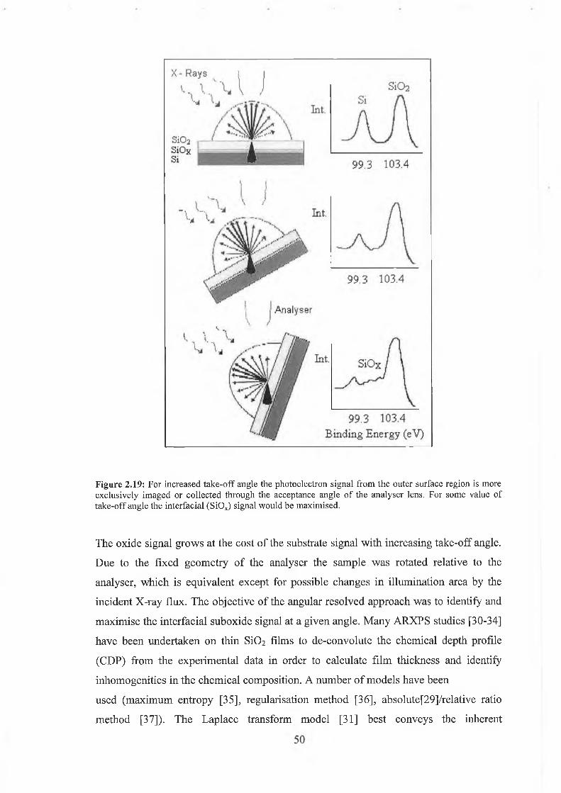
Figure 2.19: For increased take-off angle the photoelectron signal from the outer surface region is more exclusively imaged or collected through the acceptance angle o f the analyser lens. For some value of take-off angle the interfacial (SiOx) signal would be maximised.
The oxide signal grows at the cost of the substrate signal with increasing take-off angle.
Due to the fixed geometry of the analyser the sample was rotated relative to the
analyser, which is equivalent except for possible changes in illumination area by the
incident X-ray flux. The objective of the angular resolved approach was to identify and
maximise the interfacial suboxide signal at a given angle. Many ARXPS studies [30-34]
have been undertaken on thin SiC>2 films to de-convolute the chemical depth profile
(CDP) from the experimental data in order to calculate film thickness and identify
inhomogenities in the chemical composition. A number of models have been
used (maximum entropy [35], régularisation method [36], absolute[29]/relative ratio
method [37]). The Laplace transform model [31] best conveys the inherent
mathematical difficulties associated with de-convoluting a CDP. Recalling the equation
for peak intensity (equation 2.14) and considering for a dielectric layer the peak
intensity ratios (Si2P/Ois) rather than considering absolute peak intensities, then the
terms K, T(E|<), Ly(y), and cry cancel.
1 (0 ,4 j = K T (E k ) L ij ( y K j n j (z ) \ d z Equation 2.14e ^(Ek)Cose
This removes the complication arising out of angle dependent area of illumination and
analyser response. Using the change of variables p(0)=(X,cos0)’’ gives, equation 2.26,
where L denotes the Laplace transform.
l ( p ) = Jn(z)^-dz = L[n(z,p)] Equation 2.26
ez
Equation 2.26 is concerned with the intensities observed for a known CDP. Ours is the
inverse problem of finding the CDP from measured peak intensities as given by:
c(z) = L“1 [l(p ), z] Equation 2.27
The inversion of the Laplace transform is not straightforward. An analytical expression
for I(p) is not available, instead there is a set of numerical measurements. The inversion
problem is “ill posed” in that there isn’t a single suitable CDP, but a set of equivalent
profiles which satisfy the transformation. The inverse transform is very sensitive to
noise in the input data and so there is a trade-off between uncertainty in composition
with depth resolution. Cumpson et al [38] have reviewed ARXPS to date and
highlighted the importance of the precision (which must be a few percent) of intensity
measurements at the chosen emission angles rather than accuracy, if a successful de-
convoluton is to be performed. ARXPS analysis was deemed to be prohibitively
expensive in terms of complexity, time, cost of implementation of a working computer
model.
51
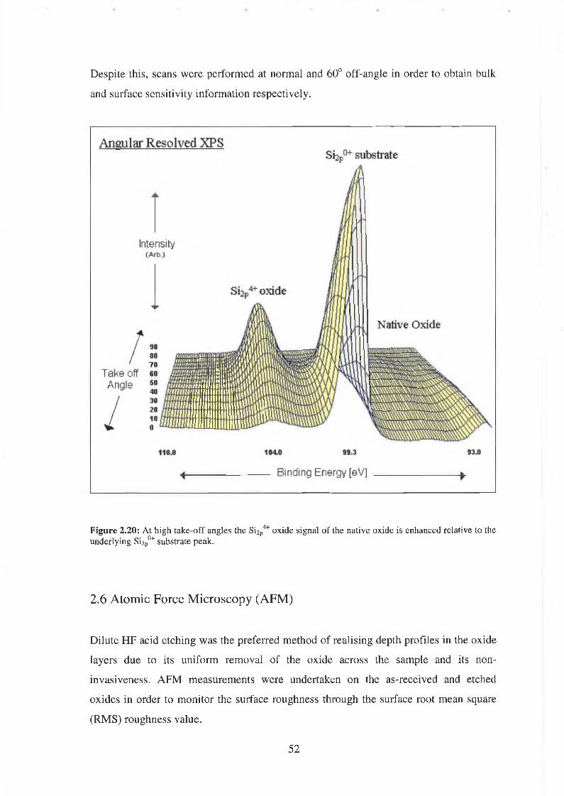
Despite this, scans were performed at normal and 60° off-angle in order to obtain bulk
and surface sensitivity information respectively.
Figure 2.20: At high take-off angles the Si2p4+ oxide signal of the native oxide is enhanced relative to the underlying Si2p0+ substrate peak.
2.6 Atomic Force Microscopy (AFM)
Dilute HF acid etching was the preferred method of realising depth profiles in the oxide
layers due to its uniform removal of the oxide across the sample and its non-
invasiveness. AFM measurements were undertaken on the as-received and etched
oxides in order to monitor the surface roughness through the surface root mean square
(RMS) roughness value.
52

The instmment used was a multimode Digital Instruments nanoscope III which can
operate in both contact and non-contact modes. In AFM a sharp tip is brought into
contact or into close contact with a surface. As the tip approaches the sample it
experiences an interaction with the surface, the extent of which in terms of magnitude
and whether the interaction is attractive or repulsive is governed by the shape of the van
der Waals force curve as shown in Figure 2.21 [39].
F igure 2.21: The sign and magnitude of the van der Waals force between tip an sample is dependent on the tip sample separation (Thermo micro [39]).
In contact mode the deformation of the cantilever to which the tip is attached is
monitored via DC signal representing the voltage required to maintain a constant value
of tip sample force. For vibrating modes of operation (i.e. non-contact and tapping) the
resonant frequency of the oscillating cantilever varies as the square root of its spring
constant. The spring constant of the cantilever varies with the force gradient
experienced by the cantilever. The force gradient, which is the derivative of the curve
shown in Figure 2.21 changes with tip-to-sample separation. In this way changes in the
resonant frequency of the cantilever can be used as a measure of changes in the force
gradient, which reflects changes in tip-to-sample spacing, or sample topography [39].
53

2.6.1 Contact Mode AFM
Figure 2 .2 2 [40] illustrates the contact m ode AFM process. A sharp tip with a radius o f
curvature o f approxim ately 30 nm is attached to a relatively soft cantilever. The bending
o f the cantilever is actuated in a precise w ay by application o f a suitable voltage to the
piezo to w hich either the sam ple or cantilever is attached. In contact m ode the tip
sam ple d istance is such that the lip sam ple interaction is predom inately repulsive with a
mean value o f 10 9 N [42],
Figure 2.22: In contact mode AFM a sharp tip in contact with a surface is rastered across the sample. The initial contact is established by application o f a suitable voltage to the piezo tube. The resultant bending of the cantilever is interpreted precisely by the photo diode through the extent o f the deflection o f the laser light reflected from the cantilever (Mauritz [40]).
T his force is ach ieved by pushing the cantilever against the sam ple surface by
application o f a suitable voltage to the p iezo tube. The deflection o f the cantilever is
sensed by the deflection o f the reflected laser light on the quadrant d iode detector and
com pared in a D C feedback am plifier to som e desired value o f deflection . If the
measured d eflection is different from the desired values the feedback am plifier applies a
suitable voltage to the p iezo to raise or low er the sam ple relative to the cantilever to
54
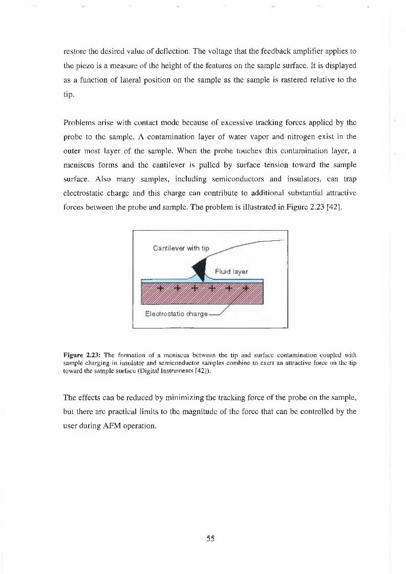
restore the desired value of deflection. The voltage that the feedback amplifier applies to
the piezo is a measure of the height of the features on the sample surface. It is displayed
as a function of lateral position on the sample as the sample is rastered relative to the
Problems arise with contact mode because of excessive tracking forces applied by the
probe to the sample. A contamination layer of water vapor and nitrogen exist in the
outer most layer of the sample. When the probe touches this contamination layer, a
meniscus forms and the cantilever is pulled by surface tension toward the sample
surface. Also many samples, including semiconductors and insulators, can trap
electrostatic charge and this charge can contribute to additional substantial attractive
forces between the probe and sample. The problem is illustrated in Figure 2.23 [42],
F igure 2.23: The formation of a meniscus between the tip and surface contamination coupled with sample charging in insulator and semiconductor samples combine to exert an attractive force on the tip toward the sample surface (Digital Instruments [42]).
The effects can be reduced by minimizing the tracking force of the probe on the sample,
but there are practical limits to the magnitude of the force that can be controlled by the
user during AFM operation.
55
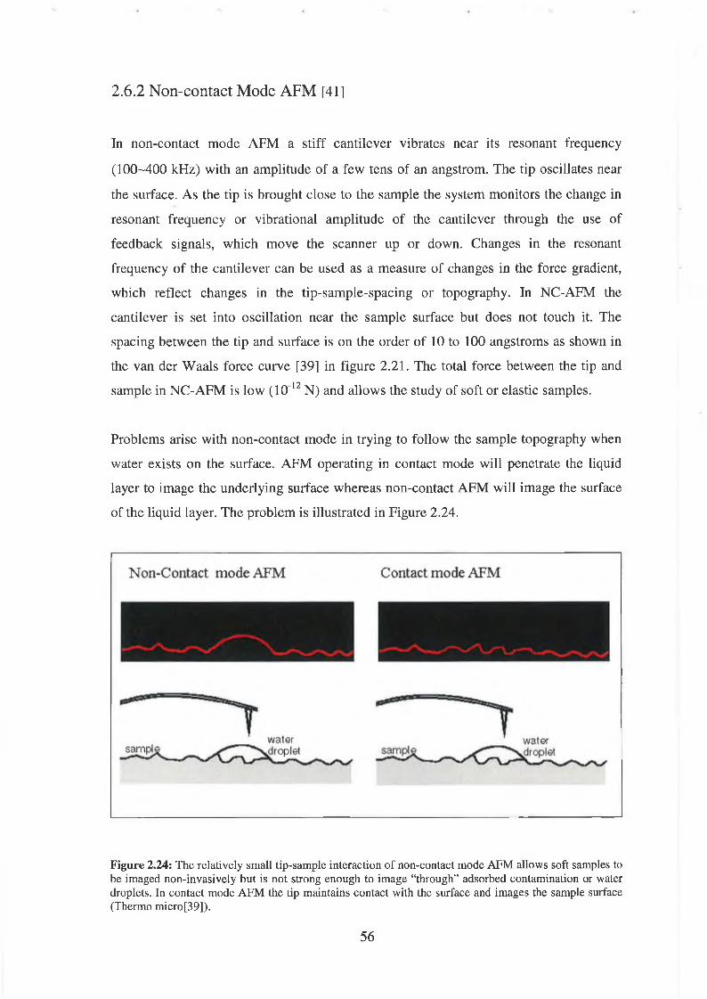
2.6.2 Non-contact Mode AFM [41]
In non-contact m ode A F M a stiff cantilever vibrates near its resonant frequency
(1 0 0 -4 0 0 kH z) w ith an am plitude o f a few tens o f an angstrom. T he tip oscilla tes near
the surface. A s the tip is brought c lo se to the sam ple the system m onitors the change in
resonant frequency or vibrational am plitude o f the cantilever through the use o f
feedback signals, w hich m ove the scanner up or down. C hanges in the resonant
frequency o f the cantilever can be used as a m easure o f changes in the force gradient,
which reflect changes in the tip -sam ple-spacing or topography. In N C -A FM the
cantilever is set into oscilla tion near the sam ple surface but does not touch it. The
spacing b etw een the tip and surface is on the order o f 1 0 to 1 0 0 angstrom s as show n in
the van der W aals force curve [39] in figure 2 .21 . The total force betw een the tip and
sam ple in N C -A F M is lo w (10 12 N ) and a llow s the study o f soft or elastic sam ples.
Problem s arise w ith non-contact m ode in trying to fo llo w the sam ple topography when
water ex ists on the surface. A F M operating in contact m ode w ill penetrate the liquid
layer to im age the underlying surface w hereas non-contact A FM w ill im age the surface
o f the liquid layer. The problem is illustrated in Figure 2 .24.
Figure 2.24: The relatively small tip-sample interaction of non-contact mode AFM allows soft samples to be imaged non-invasively but is not strong enough to image “through” adsorbed contamination or water droplets. In contact mode AFM the tip maintains contact with the surface and images the sample surface (Thermo micro[39]).
56

In order to ach ieve h igh resolution (vertical) in non-contact m ode A FM , it is necessary
to m easure force gradients from van der W aals forces, w hich m ay extend only a
nanom eter from the sam ple surface. G enerally the flu id contam ination layer is
substantially thicker than the range o f the van der W aals force gradient and therefore,
attempts to im age the true surface fa ils as the oscilla ting probe becom es trapped in the
flu id layer or hovers beyond the effec tiv e range o f the forces it attempts to measure.
2.6.3 Tapping Mode AFM [40]
For the ox id e layers considered in this thesis the A F M w as operated in non-contact
tapping m ode. T he operation process is illustrated in Figure 2 .25 [40].
Tapping Mode Atomic Force Microscopy
(3) Amplitude Data Laser
(1) Height Dataz-axis position m onitored by input voltage to piezo tube scanner
Piezo driver
w(2) Phase Data (i)P hase o f drive signal com pared to phase ofoutput signal from photo diode detector
Sample Sirface
Figure 2.25: A sharp tip oscillates at the natural frequency of the cantilever to which it is attached. When the tip is brought close to the sample surface it’s oscillation phase and amplitude are modified through Van der Walls interaction. The distance between the tip and sample is regulated through the voltage applied to the piezo, the extent of which is decidcd by the feedback signal from the detector to the piezo driver (Mauritz [40]).
57

In tapping m ode, the silicon probe tip oscilla tes at the resonant frequency o f the
cantilever to which it is attached. T he oscillating tip is rastered across the sample
surface line by line. W hen it approaches the surface the tip interacts with the surface
through Van der W alls forces w hich m odify its am plitude and phase o f oscillation.
T hese m odifications are m easured at a four quadrant (a llow in g both vertical and lateral
force m icroscopy) d iode detector through the change in position and phase o f laser light
reflected from the oscilla ting tip.
, lOM-mCalibration Suriace
»1 0 |_im
Figure 2.26: (Top) CCD image ( - 20 |xm x 180 |im) from auxiliary magnification stage of calibration standard sample. Vert. Defl is almost zero as light reflected from tip on quadrant detector is almost in the centre. The RMS amplitude is that o f free vibration. Sum is an indication of the extent of the reflection from tip. (Below) a simplified 3D schematic of the known surface topography.
58

T he capabilities and lim itation o f tapping m ode A F M are best expressed by considering
its ability to map out a know n topography. Figure 2 .2 6 show s a calibration surface with
know n dim ensions. T he surface is m ade up o f a periodic square array o f w ells o f length
10 (j,m and depth 0 .2 |j,m and separated by 10 [am. Figure 2 .27 show s a high resolution
tapping m ode A FM im age o f a sing le w e ll structure in the calibration standard. H eight
is interpreted in terms o f colour. The fu ll z height is 0 .4 |im and so a feature this high or
higher w ill be seen as w hite w here as sm aller features as seen as darker red.
Figure 2.27: Tapping mode image o f a single well structure from the calibration standard in (a) height mode and (b) amplitude mode.
T he data is presented in tw o m odes, height and am plitude. There are three formats in
w hich data can be presented.
Height Data: The vertical position o f the probe tip is m onitored by noting changes in
the length o f the z-a x is on the xyz scanning p iezo tube. Input voltage to the scanning
p iezo tube is proportional to the length o f the tube. The change in the z-ax is is plotted as
a topographical map o f the sam ple surface. H eight data is a good m easure o f the height
o f surface features but does not show distinct ed ges o f these features.
59
Amplitude D ata : T he am plitude o f the cantilever is m onitored by the photo diode
detector. T he R M S value o f the laser signal on the y -ax is o f the detector is recorded for
each o f the 5 12 segm ents on a g iven raster o f the probe tip. T hese values are plotted as
an am plitude m ap o f the sam ple surface. A m plitude im ages tend to sh ow edges o f
surface features w ell.
Phase Data: T his type o f im aging m onitors the change in phase offset, or phase angle,
o f the input drive signal to the drive p iezo w ith respect to the phase o ffset o f the
oscillating cantilever. The phase o f the drive signal (i) is com pared to the phase o f the
cantilever response signal (ii) on the photo d iode detector. S ee (2) in the above figure
2.25 . The p hase o ffse t betw een the tw o signals is defined as zero for the cantilever
oscilla ting freely in air. A s the probe tip engages the sam ple surface, the phase o ffset o f
the oscilla ting cantilever changes by som e angle w ith respect to the phase o ffset o f the
input drive signal. A s regions o f d iffering elasticity are encountered on the sample
surface, the p hase angle b etw een the tw o signals changes. T hese changes in phase offset
are due to d iffering am ounts o f dam ping experienced by the probe tip as it rasters across
the sam ple surface. T hese d ifferences are plotted as the so -ca lled “phase im age”.
In addition to the m onochrom e intensity inteipretation o f the surface topography, the
current “lin e” b eing scanned or rastered can be v iew ed in scop e m ode w here the trace
and retrace o f the lin e scan can be superim posed to gauge the stability o f the scan and
also to op tim ise the feedback controls o f proportion and integral gain.
The sen sitiv ity o f am plitude m ode to sharp features is ev ident in figure 2 .28 from the
relatively large signal associated w ith the local trace/re-trace disagreem ent at the
“sharp” w e ll ed ges in am plitude m ode com pared to h eight m ode.
U nlike the above calibration standard the surface o f an industrial ox ide is not know n
exactly but is exp ected to be flat on a sub nanom eter sca le w ith a surface roughness
characterised by it ’s R M S value o f peak heights about the m ean height on the surface.
A FM is d iscu ssed in this context in chapter 4.
60
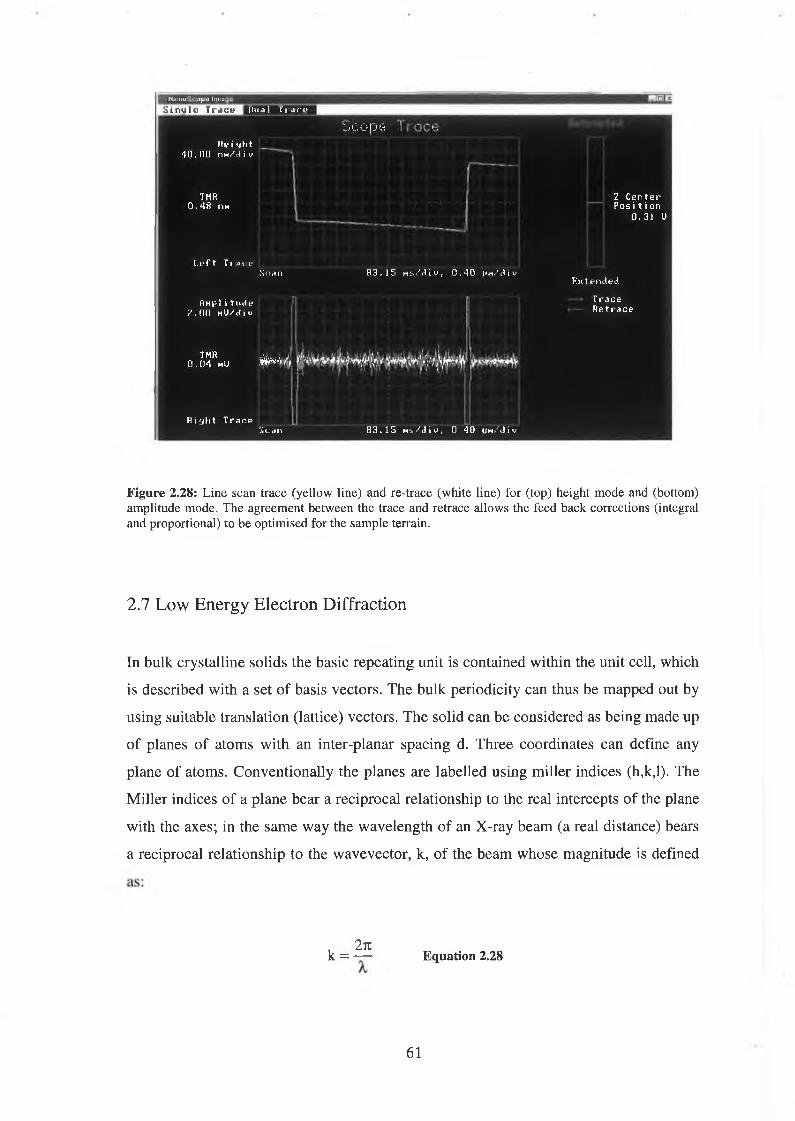
N f i i m .I [_ I.: In » iv
Sinule ïrdcw Dun)Traoc
II« ¡»lit ■111. I)II MM/.iiu
TMR 0, 48 rm
Left TraceScan
flhpIi tuJe 2 . 0 0 hU/<Jìu
I MB Uow,0 . 04 hU Jr**1-'
:-.'COpe
R3.I5 Hs/dîv» O.^O UM^diw
R i g h t T r a c e
2 Center Pos i t i on
0.31 U
Extended
Trace Re t r ace
Scan 8 3 . 1 5 H s ^ d i y , 0 . 4 0 uH^div
Figure 2.28: Line scan trace (yellow line) and re-trace (white line) for (top) height mode and (bottom) amplitude mode. The agreement between the trace and retrace allows the feed back corrections (integral and proportional) to be optimised for the sample terrain.
2.7 Low Energy Electron Diffraction
In bulk crystalline so lid s the basic repeating unit is contained w ithin the unit ce ll, which
is described w ith a set o f basis vectors. The bulk periodicity can thus be mapped out by
u sing suitable translation (lattice) vectors. T he so lid can be considered as being made up
o f planes o f atom s w ith an inter-planar spacing d. Three coordinates can define any
plane o f atom s. C onventionally the planes are labelled using m iller ind ices (h,k,l). The
M iller ind ices o f a p lane bear a reciprocal relationship to the real intercepts o f the plane
w ith the axes; in the sam e w ay the w avelength o f an X-ray beam (a real distance) bears
a reciprocal relationship to the w avevector, k, o f the beam w hose m agnitude is defined
2 kk = —— Equation 2.28
61
The w ave vector is a m easure o f the m om entum o f the incident and diffracted beam s.
The change in w avevector o f a beam on scattering from a p lane o f atom s w ill determine
the direction o f any em ergent diffracted beam s. In Figure 2 .2 9 [43] the diffraction
condition is readily evaluated using the principle o f conservation o f m om entum .
Figure 2.29: The Ewald sphere construction for a cubic lattice, (h,k,l) are the miller indices of the point on the Ewald sphere (Prutton [43]).
The w avevector o f the incident X -ray is represented b y ko and is elastically scattered
(i.e. no change in energy) through an angle 2 0 to k resulting in a m om entum change.
The B ragg d iffraction cond ition requires:
nA, = 2 d S in (0 ) Equation 2.29
T h e c o n d i t io n is s a t is f ie d w h e n th e c h a n g e in m o m e n tu m (A k = k ’-k o ) is e q u a l to a
r e c ip ro c a l la tt ic e v e c to r . T h e la tt ic e s h o w n is th e r e c ip ro c a l la t t ic e , w h e re th e d is ta n c e
b e tw e e n a d ja c e n t p o in ts is 27i/d, w h e re d is th e d is ta n c e b e tw e e n p o in ts in r e a l sp ace .
62
A circle w ith radius ko is drawn and is the E w ald sphere. The p osition o f the diffracted
beam s offers inform ation about the crystal lattice size and sym m etry. A n alysis o f the
intensity g ives inform ation about the arrangement o f atom s w ith in the lattice (the crystal
basis). The pattern produced by the crystal as a w h o le depends on the number o f atoms
in each unit ce ll and on their p osition s relative to one another.
A surface ex ists in tw o d im ensions w here the p eriod icity o f the underlying crystal in the
direction norm al to the surface is lost. On a surface there is period icity w here the basic
repeating unit is contained w ith in a surface unit m esh, w h ich can be m apped out w ith
translation vectors. H ow ever, X -rays are lim ited in their use to probe the periodicity o f
the surface b ecau se o f the sm all scattering interaction b etw een X -rays and the charge
distribution on atom s, w h ich results predom inately in bulk inform ation, w h ich w ould
dom inate the sm aller surface signal. L ow energy electrons, how ever, have a very strong
interaction w ith m atter and have a short m ean free path (for E < 150 eV ). T he w avelength
o f such electrons is sligh tly sm aller (a few angstrom s) than the typ ical inter-atom ic
spacing and therefore suitable for diffraction experim ents. F igure 2 .3 0 [44] show s an
incident w av e v ec to r sc a tte re d w av e v ec to r d istance b e tw e e n sca tters
4)= angle o f incidence V = exit angle 9 = diffraction angle ko= incident w av e vec to r k ’= sc a tte re d w av e v ec to r g = ko - k’
k<,= k ’ = d =
Surface
Figure 2.30: A schematic diagram o f a diffraction process occurring at a surface in real space (a), with the corresponding Ewald sphere construction in reciprocal space (b) (Vickerman [44]).
63

electron characterised by a w avevector ko incident on a clean surface, the electron is
scattered b y the outer atom s w h o se separation is d. B ecau se the surface is tw o
dim ensional the repeat d istance norm al to the surface is infinite and so the reciprocal
lattice “poin ts” a long the surface normal are in fin ite ly c lo se form ing rods. The
diffraction condition is satisfied for every beam that em erges in a direction along w hich
the sphere intersects a reciprocal rod. L ike in X -ray diffraction, the position o f the spots
in a LEED pattern can be used to determ ine the s ize and sym m etry o f the surface unit
m esh.
In three d im ensions there are 14 different B ravis lattices. In tw o dim ensions there are
f iv e different surface nets. In any net every lattice poin t can be reached from the origin
by translation vectors
T = m as + nbs E quation 2.30
Figure 2.31: (a) square surface net, (b) (Top) real space ( lx l ) surface reconstruction, (Bottom) it’s corresponding reciprocal space LEED pattern, (c) (Top) real space (2x1) surface reconstruction, (Bottom) its corresponding reciprocal space LEED pattern [45].
64

W here m and n are integers, and the vectors as and bs define the unit m esh. Figure 2.31
[45] (a) sh ow s the square system . Figure 2.31 (b) sh ow s an unreconstructed surface and
it’s corresponding LEED pattern. W hen the surface reconstructs, the surface can be
m apped u sing m ultip les o f the translation vectors o f the unreconstructed surface. In
Figure 2.31 (c) (Top) the atom ic spacing o f the outerm ost atom s in the x direction is
tw ice the value that w ou ld ex ist in an unreconstructed surface. The spacing in the y
direction is the sam e and so the m ultiples on the x and y translation vectors are 2 and 1
denoting a 2x1 reconstruction. In reciprocal space (bottom ) the scaling o f the x and y
lattice points has been inverted.
Figure 2 .3 2 sh ow s a LEE D system , w hich a llow s the period icity o f a surface to be
investigated. A n electron beam o f variable energy is produced by an electron gun and is
incident on the sam ple.
Figure 2.32: In a LEED experiment a beam of monochromatic low energy electrons is incident on the clean surface. The electrons are backscattered from the sample surface onto a system o f grids. Only the elastically scattered electrons form the LEED pattern and are accelerated towards a fluorescent screen where a pattern o f bright spots is seen. The inelastically scattered electrons are rejected by the negative potential o f the other two grids.
65
B oth elastic and inelastic electrons are backscattered onto a system o f grids surrounding
the gun. A fter reaching the first grid G i (w hich is earthed) e lastica lly scattered electrons
are accelerated tow ards a fluorescent screen w here a pattern o f bright LEED spots is
seen. The grids G 2 and G 3 are held at an adjustable n egative potential in order to reject
m ost o f the inelastica lly scattered electrons, w h ich contribute to the d iffuse background.
2.8 Synchrotron Radiation
W hen a charged particle (electron or positron) is m ade to traverse a curved (circular)
path by say a m agnetic fie ld as show n in figure 2 .33 [46] the charged particle em its
electrom agnetic radiation in a direction tangential to its centripetal acceleration.
Figure 2.33: Radiation pattern for an orbiting charge in a magnetic field (Hecht [46]).
In a synchrotron radiation source a beam o f electrons is injected into a storage ring,
w h ich is under U H V . T he electrons are accelerated to energies o f the order o f G eV by a
radio frequency (R F ) accelerating cavity operated in phase w ith the arrival o f the
electron bunches. T he electrons travel in bunches c lo se to the speed o f light and are
66
confined to a circular path by bending and focusin g m agnets. B ecau se the electrons are
travelling at relativistic speeds the S R is em itted in a narrow cone in a tangential
direction from the bending curve at the tim e o f em ission . The em itted radiation is
broadband (i.e. the high tem poral localisation is realised through the addition o f many
frequencies), extrem ely intense, co llim ated and h igh ly p lane polarized (w hich facilitates
w avelength selection). In a synchrotron facility the radiation is collected through
beam lines, w hich are tangential to the ring. Figure 2 .3 4 [48] show s a schem atic o f a
typical synchrotron light source facility with experim ental beam lines attached.
Injector(LINAC)
Scheme o f a Synchrotron Light Facility I
Injection Line
CirculatingElectrons
Storage BendingRing (UHV) Magnet
iBeamline
Experimental R.F.Chamber Cavity
ExperimentalChamber
Figure 2.34: A schematic representation of a synchrotron radiation facility [48],
T he advantages o f synchrotron light for photoem ission are in its intensity, its resolution,
the ability to tune the energy (frequency) o f the light. T hese properties allow the energy
dependence o f surface sen sitiv ity to be exp lo ited and thus depth profile a sam ple in the
sub-nanom eter regim e or to reso lve c lo se ly in g chem ical states. In angle resolved
photoem ission (U P S) the w a v e nature o f synchrotron (polarisation o f the E field) light is
exp lo ited in order to probe (“m ap”) the electronic structure o f m aterials [2 ],
67
Insertion devices [48]:
Electrons are injected into a storage ring in bunches, but on each pass each bunch
illum inates any g iv en beam line on ly once. B y forcing electrons to fo llo w a zigzag path
a beam line located at the end o f such a path can co llec t ligh t several tim es per turn
instead o f once. T he change in the electron trajectory is ach ieved u sing insertion devices
such as a w igg ler or undulator. In a w igg ler or undulator electrons travel through a
periodic m agnetic structure.
Wiggler
A w igg ler w orks as fo llow s; it con sists o f a periodic series o f m agnets, p laced in a ring
section w here the electron path w ou ld otherw ise be straight; because o f it ’s action, the
electrons are forced to “w ig g le ” around the straight path resulting in a very high flux o f
X -rays along the w igg ler beam line.
Undulator
A n undulator is sim ilar to a w igg ler excep t it forces the electrons into a m uch weaker
zigzag , so that during the entire z ig za g m otion synchrotron light continues to illum inate
the undulator beam line. W ithout short pulses, there is no w id e band o f w avelengths,
thus the undulator em ission is not spread in a w id e band but concentrated, producing
high lev e ls o f flu x and brightness.
2.8.1 NSLS U4A Beamline Characteristics
Soft X -ray p h otoem ission experim ents w ere perform ed on beam line U 4 A at the
N ational Synchrotron L ight Source (N S L S ) at B rookhaven N ational Laboratory, N e w
York. T his fac ility is a second-generation light source w ith an X -ray and vacuum ultra
v io le t (V U V ) ring. T he function o f the beam line is to gather and m onochrom ate the
light em itted from the ring and finally focus the light into as a sm all spot onto the
sam ple in the analysis chamber. Figure 2 .35 sh ow s the optical layout o f the beam line.
68

Figure 2.35: A schematic representation o f the optical layout o f beamline U4A. Light enters the line and is bent and focused onto the entrance slit to the monochromator by the front-end mirror. The monochromator selects the desired wavelength through dispersion. The exit slit focuses the light onto the sample in the analysis chamber.
The line is on bending m agnets on the (0.8 G eV ) U V ring, and can deliver light from 8
to 2 5 0 eV u sing three interchangeable gratings. The front-end mirror co llects light
directly from the bending m agnet and focu ses the light on to the m onochrom ator
gratings. The m onochrom ator is a 6 m /1600 toroidal grating instrument, w ith three
gratings w ith 2 8 8 , 822, and 2 4 0 0 lines per m m . The diffracted light passes through the
ex it s lit w h ich is m ounted on a linear drive for beam optim isation. Finally the beam
illum inates the sam ple in the analysis chamber.
The analysis cham ber is equipped w ith a V S W analyser w ith co llection lens. The
sam ple m anipulator a llow s x y z linear m otion and rotation; a lso a sam ple can be heated
by electron beam heating. T he analysis chamber is equipped w ith a LEED system and
an inert ion sputter gun for sam ple cleaning. U H V is ach ieved using suitably arranged
rotary, turbo m olecular and io n pum ps. A FEL cham ber is connected to a preparation
cham ber w h ich is its e lf connected to the analysis chamber. This allow ed the
introduction o f a sam ple from air into U H V w ith in 10 m inutes v ia a sam ple transfer
m echanism . The analysis cham ber is presented in m ore detail in chapter 6 .
69

2.8.2 Synchrotron considerations
W ith excellen t resolution and tuneable surface sen sitiv ity synchrotron radiation allow s
the sam pling depth to be varied and also c lo se ly in g chem ical states to be resolved.
There m ay be som e evolu tion in a spectrum w ith different photon energy due to a
change in the shape o f the background or the photoion isation cross-section or in
resolution due to the response cure o f the m onochrom ator grating.
Background removal
The surface sen sitiv ity o f a photoelectron is m axim ized for a kinetic energy o f ~ 40 eV ,
and so for S i2 P (Eb 99 .3 eV ), surface sen sitiv ity is m axim ized u sing a photon energy o f
130 eV . Figure 2 .3 6 sh ow s a S i2 P spectrum taken by H ollin ger et al [49] at photon
energy o f 1 2 0 eV .
Processing of Sijp Core Level Spectra
K
i i t i i r i i :
Sit11W 7x7H 0O 0L<^ a
's 's. I
h v = 120 eV
rv /\ V /
X ,
\ f 1 B ackground
\ Afl I \ hv = 112 eVD if f e r e n c e '^ / f
Spin-Orbit Decom posed y C /
« i i i t i i10 11 12 13 H 15 16 17 IS 1« 20
KINETIC ENERGY (s V )
Figure 2.36: The background on which the Si2p spectral envelope sits can be sampled in isolation of the Si2p peak by considering the same energy window at a different photon energy. After subtracting the estimated background the redundant Sipi/2 component o f the spin orbit degeneracy is numerically removed in a spin stripping process (Hollinger [49]).
70
D ifficu lties arise w hen look ing “deeper” into the surface w ith a m ore bulk sensitive
photon energy o f 120 eV . A t 120 eV the peak sits quite h igh on the secondary electron
background (see figure 4 .25 , chapter 4), w h ich com plicates background rem oval. B y
taking spectra in the sam e kinetic energy w in d ow but at different photon energies ( 1 1 2
and 120 eV ) the background on w h ich the peak sits can be seen in iso lation o f the peak
thus a llow ing background subtraction. H ow ever as d iscussed earlier, there are extrinsic
processes, and intrinsic p rocesses inherent in the p h otoem ission process which
contribute to the peak intensity w h ich could be unfairly subtracted in the approach
above. T herefore w h en dealing w ith sam ples o f a h igh doping or at bulk sensitive
photon energies the background w as sam pled at a reduced photon energy and the
rem aining intrinsic lo ss process w as approxim ated w ith a Shirley background.
Spin orbit stripping
W hile synchrotron light offers excellen t resolution com pared to conventional XPS
sources, its resolution is fin ite and not alw ays able to clearly reso lve overlapping peaks.
For S i2 P the constant branching ratio and spin-orbit sp litting b etw een the Si2 P3 /2 and
Si2 Pi / 2 com ponent a llow s num erical subtraction o f the sm aller 2 p i / 2 com ponent starting
on the h igh kinetic energy side o f the peak and im plem enting the fo llo w in g algorithm:
Intensity[E k] = Intensity[Ek]+ (0.5Intensity[E k + spin orbit sp lit]) Equation 2.31
w here Intensity [Ek] is the intensity at k inetic energy E^.
Figure 2 .3 7 sh ow s a SiC>2 spectrum , after background rem oval. The red line show s the
raw data and the black the spectrum after spin stripping. T he background m ust first be
rem oved before starting the spin-stripping algorithm .
Care m ust be taken not to introduce “artefacts” into the spectrum , as typically the
spectrum is interpolated before stripping. The danger is that a “sp ike” or “artefact”
m ade up o f on ly tw o points in the raw data w ou ld span fiv e points in the interpolated
data and looks m ore like a legitim ate peak. The point is illustrated in the inset in figure
2.30 w here a local sp ike ex ists in the raw data.
71

H ow ever w ith careful exam ination o f the raw data and rem oval o f spikes, spin-orbit
stripping is u sefu l in elucidating the structure in the S i2 P3 / 2 spectral envelope.
Kinetic energy [eV]
Figure 2.37: A high resolution Sii,, photoelectron spectrum (red) has the Si2pi/2 component o f the spin- orbit degeneracy removed numerically in order to better elucidate structure in the spectral envelope through the Si2p3/2 component (black). The inset illustrates how a localised spike (single point) in the raw data can be propagated into a more legitimate peak (three points) through interpolation before stripping.
72
2.9 References for Chapter II
1 M. Cardona. L. L ey (Eds.). P h otoem ission in Solids. Parts 1 and 2. Springer.
Berlin. 1978
2 K .E. Sm ith, P hysics Dept. B oston U niversity, Subm itted for publication
3 S. H ufner, Photoelectron Spectroscopy. Solid State S cien ces, ed. Springer. 1995
4 Private C om m unication, Prof. I. T. M cG overn, P hysics D ept. Trinity C ollege
D ublin
5 X -ray data booklet, Law rence B erk eley N ational Laboratory
6 K. Siegbahn, C. N ordling, A . Fahlm an, N o v a A cta S ocietatis Scientiarum U p salien sis, Ser. IV , 2 0 (1967) 5
7 F. H im p sel, F. M cF eely , A . Taleb-Ibrahim i, J. Y arm off, G. H ollinger, Phys. Rev.
B 3 8 (1 9 9 8 ) 6 0 8 4
8 B . D . Ratner chpt 3, p 52 , Surface A n alysis the Princip le T echniques, J. Vickerman,
W iely & Sons (1997) p52
A . Pasquarello, M .S . H ybertsen, R. Car, Phys. R ev. Lett. 74 (1 9 9 5 ) 1024
1 0 M . B anaszak H oll, S. L ee, F.R. M cF eely , Appl. Phys. Lett 72 (1 9 9 3 ) 2441 also M.
B anaszak H oll, S. L ee, F.R. M cF eely , A ppl. Phys. Lett 65 (1 9 9 4 ) 1097
11 B. Ratner, Surface analysis - the principal techniques, J. V ickerm an, W iely &
Sons (1 9 9 7 ) p .49
1 2 M .P . Seah and W .A . D ench , Surf. Interface A nal. 1 (1 9 7 9 ) 2
13 V acuum S cien tific (V G ) instrum ent m anual for C lam analyser
1 4 B riggs and Seah, Practical Surface S cien ce, 2 nd Edt. W iely & S on s(1994) p 76
15 S. Tougaard, Surf. Interface A nal., 11 (1 9 8 8 ) 453
1 6 A .M . Salvia , J.E. Castle, J. E lectron Spectrosc. Relat. Phenom . 95 (1998) 45
1 7 D .A . Shirley, Phys. R ev. B 5 (1 9 7 2 ) 4709
18 P. B ev in ton , D ata R eduction and Error A n alysis for the Physical Sciences;
M cG raw -H ill B o o k C om pany : N e w Y ork 1992
1 9 B . Ratner, Surface A n alysis - the Principal T echniques, J. V ickerm an, W iely &
S o n s (1 9 9 7 ) p .60
73
2 0 J.H. S co fie ld , H. Slater, J. E lectron Spectrosc. Relat. Phenom ., 8 , (1976) 129
21 C. P ow ell, J. E lectron Spectrosc. Relat. Phenom . 4 7 (1 9 8 8 ) 197
2 2 J. Shallenberger, J. V ac. Sci. T echnol. A 1 4 (1 9 9 6 ) 693
2 3 J. Shallenberger, D . C ole, S. N ovak , A 1 7 (1 9 9 9 ) 1086
2 4 J.H. T hom as III, S. H ofm ann, J. V ac. Sci. T echnol. A3 (1985)1921
2 5 S. E vans, R. G. Pritchard, J. M . Thom as J. E lectron Spectrosc. Relat. Phenom . 14
(1 9 7 8 ) 341.
2 6 R .I.H egde, M aiti, R .S.R ai, K. G. R eid, and P.J. Tobin, J. E lectrochem . Soc. 145
(1 9 9 8 ) L13
2 7 H. C. Lu, E. P. G usev, T. G ustafsson, E. Garfunkel, M . L. G reen, D . Brasen, and
L. Feldm an, A ppi. Phys. Lett. 69 (1 9 9 6 ) 2713
2 8 S. R. K aluri, and D . W. H ess, Appi. Phys. Lett. 69 (1 9 9 6 ) 1053
2 9 S. H ashim oto, K. Hirokawa, Y . Fukuda, N . U su k i, N . G ennai, S. Yoshida, H.
H orie, A . Tanaka, and T. Ohtsubo, Surf. Interface A nal. 18 (1 9 9 2 ) 799
3 0 J.E. Fulghum , Surf. Interface A nal., 20 (1 9 9 3 ) 161
3 1 T .D . B u ssin g and P.H. H o llow ay , J. V ac. Sci. T echnol. A 3 (1 9 8 5 ) 1973
3 2 W . A am ink , A . W eishaupt, A . S ilfhout, A ppi. Surf. Sci. 45 (1 9 9 0 ) 37
3 3 M . E bel, Surf. Interf. A naly. 3 (1 9 8 1 ) 149
3 4 A . Ishizaka, S. Iwata, A ppi. Phys. Lett. 36 (1 9 8 0 ) 71
3 5 G. Sm ith, A . L iv esey , Surf. Interface Anal. 19 (1 9 9 2 ) 175
3 6 B. T yler, D . Castner, B . Ratner, Surf. Interface Anal. 14 (1 9 8 9 ) 443
3 7 J. H ill, D . R o y ce , C. Fadley, F. W agner, F. J. Grunthaner, Chem . Phys. Lett. 44
(1 9 7 6 ) 225
3 8 P.J. C um pson J. E lectron Spectrosc. Relat. P henom ., 73 (1 9 9 5 ) 25
3 9 Therm o M icro W eb page http ://therm om icro .com /spm guide/l-2-0 .h tm
4 0 Prof. K enneth A . M auritz Departm ent o f P olym er S cien ce U niversity o f
M ississip p i, http://w w w .psrc.usm .edu/m auritz/afm .htm l
74
'1 1 Departm ent o f C hem istry and B iochem istry, U niversity o f G uelph
http ://w w w .chem bio.uoguelph.ca/educm at/chm 729/aim /details.h tm
4 2 D igital Instrum ents W eb page
h ttp ://w w w .d i.eom /A p p N otes/S ein i/S em iM ain .h lm l#S R C l
4 3 M . Prutton, Surface P hysics, Clarendon Press, O xford (1983)
4 4 W . F lavell, Surface A n alysis - T he Principal T echn iques, J. V ickerm an, W iely &
Sons (1 9 9 7 ) p .323
4 5 S ilico n Surfaces and Form ation o f Interfaces, Jarek D abrow ski, Hans M ussig,
W orld S cien tific , Page 89
4 6 H echt, O ptics, A d d ison -W esley publishing 2 ,ul Edt. Page 50
4 8 T rieste synchrotron W eb page : w w w .elettra .trieste.it/v isitors/
4 9 G. H ollinger, F. H im psel, Phys. R ev. B 28 (1 9 9 3 ) 3651
75
Chapter 3
Chemical characterisation of thin SiON and SiC>2 films using X-rayphotoelectron spectroscopy
3.0 Introduction
This chapter is concerned w ith the chem ical characterisation o f s ilico n d ioxide and
oxynitride d ielectric layers using X PS. The primary objective w as to determ ine whether
X PS had the n ecessary resolution and surface sen sitiv ity to analyse the changes in the
dielectric sto ich iom etry in the near surface region. The as-received sam ples were
evaluated u sin g X P S in term s o f chem ical com position , th ickness and oxidation states
present in the layers. N o interfacial s ilicon suboxides w ere detected in the as-received
sam ples w h ich con sisted o f a range o f d ielectric layers 20 , 13.4, 7 .2 , 6.5 and 5.5 nm
thick as w as determ ined by ellipsom etric m easurem ents m ade fo llo w in g dielectric
growth in com m ercial furnaces. The 20 nm film w as effec tiv e ly in fin ite ly thick as the
substrate s ilico n signal could not be detected and therefore y ie ld ed good fitting
parameters for the o x id ised silicon signal. T w o different experim ental approaches w ere
used to thin the d ielectric layer w ith the sp ec ific ob jective o f analysing changes in
chem ical com p osition and oxidation states present in the near surface region. Argon
bom bardm ent w a s u sed to acquire a chem ical depth profile o f the dielectric layer, but as
w ill be show n in the results section, the bom barding process itse lf affected the FW HM
o f the core lev e l peaks and introduces suboxide core lev e l features in to the spectrum.
A s one o f the ob jectives o f the study w as to m onitor the presence o f suboxide states in
the interfacial region , the generation o f broadened peaks and suboxide sp ecies by the
bom barding p rocess ultim ately m ade th is approach untenable. The second approach
involved the th inning o f the dielectric layers using very dilute H F etching solutions. The
experim ental results for SiC>2 film s thinned in th is w ay illustrated that the peak FW H M
w as unaffected by thinning p rocesses and suboxides w ere on ly detected in the
im m ediate v ic in ity o f the d ie lectric-silicon interface.
The nitrogen signal in the as-received d ielectric layers (5 .5 and 3.3 nm ) consisted o f a
single N is ch em ical com ponent. Studies o f the evo lu tion o f th is peak w ith dilute w et
chem ical etch in g revealed the presence o f a ch em ica lly sh ifted interfacial nitrogen peak.
76
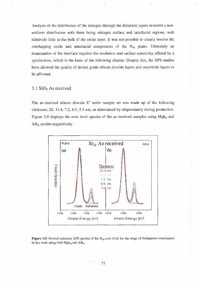
A n alysis o f the distribution o f the nitrogen through the d ielectric layers revealed a non-
uniform distribution w ith there being nitrogen surface and interfacial regions, with
relatively little in the bulk o f the ox id e layer. It w as not p ossib le to clearly resolve the
overlapping ox ide and interfacial com ponents o f the N u peaks. U ltim ately an
exam ination o f the interface requires the resolution and surface sensitiv ity offered by a
synchrotron, w hich is the basis o f the fo llo w in g chapter. D esp ite this, the X P S studies
have a llow ed the quality o f d ev ice grade silicon d iox id e layers and oxynitride layers to
be affirmed.
3.1 S i0 2 As received
The as-received silicon d ioxide 8 ” w afer sam ple set was m ade up o f the fo llow in g
thickness; 20 , 13.4, 7 .2 , 6 .5 , 5 .5 nm , as determ ined by elliposim etry during production.
Figure 3 .0 d isp lays the core level spectra o f the as received sam ples using M gka and
A lk a anodes respectively .
Kine t i c E n e r g y [eV] K ine t i c E n e r g y [eV]
F igure 3.0: Normal emission XPS spectra of the Si2p core level for the range of thicknesses investigated in this work using both M gka and Alka
77
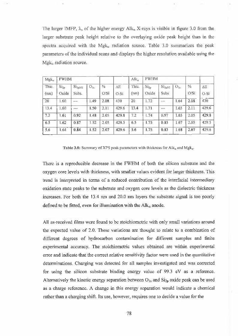
The larger IM FP, X, o f the higher energy A lk a X -rays is v is ib le in figure 3.0 from the
larger substrate peak height relative to the overlaying ox id e peak height than in the
spectra acquired w ith the M gka radiation source. T able 3 .0 sum m arizes the peak
parameters o f the individual scans and disp lays the higher resolution available using the
M gka radiation source.
Mgka FWHM Alk0 FWHM
Thic.
(nm)
Si2p
Oxide
S l2 p 3 /2
Subs.
o ls %
O/Si
AE
O-Si
Thic.
(nm)
Si2p
Oxide
S l2 p 3 /2
Subs
o ls %
O/Si
AE
O-Si
2 0 1.60 . . . 1.49 2.08 430 2 0 1.72 — 1.64 2.08 430
13.4 1.60 — 1.50 2 .1 1 429.6 13.4 1.71 — 1.65 2 .11 429.6
7.2 1.61 0.92 1.48 2.05 429.8 7.2 1.74 0.97 1.65 2.05 429.8
6.5 1.62 0.87 1.52 2.05 429.5 6.5 1.75 0.85 1.67 2.05 429.5
5.6 1.64 0.84 1.52 2.07 429.6 5.6 1.75 0.83 1.68 2.07 429.6
T able 3.0: Summary o f XPS peak parameters with thickness for Alka and Mgka.
There is a reproducible decrease in the FW H M o f both the silicon substrate and the
o xygen core lev e ls w ith th ickness, w ith sm aller va lues ev ident for larger thickness. This
trend is interpreted in term s o f a reduced contribution o f the interfacial intermediary
oxidation state peaks to the substrate and o xygen core lev e ls as the d ielectric thickness
increases. For both the 13.4 nm and 20 .0 nm layers the substrate signal is too poorly
defined to be fitted, even for illum ination w ith the A lk a anode.
A ll as-received film s w ere found to be stoichiom etric w ith on ly sm all variations around
the exp ected va lu e o f 2 .0 . T hese variations are thought to relate to a com bination o f
different degrees o f hydrocarbon contam ination for different sam ples and finite
experim ental accuracy. The stoichiom etric values obtained are w ith in experim ental
error and indicate that the correct relative sensitiv ity factor w ere used in the quantitative
determ inations. C harging w as detected for all sam ples investigated and w as corrected
for u sing the s ilico n substrate binding energy value o f 99.3 eY as a reference.
A lternatively the k inetic energy separation betw een O is and S i2 P ox id e peak can be used
as a charge reference. A change in this energy separation w ou ld indicate a chem ical
rather than a charging shift. Its use, how ever, requires one to d ecide a value for the
78
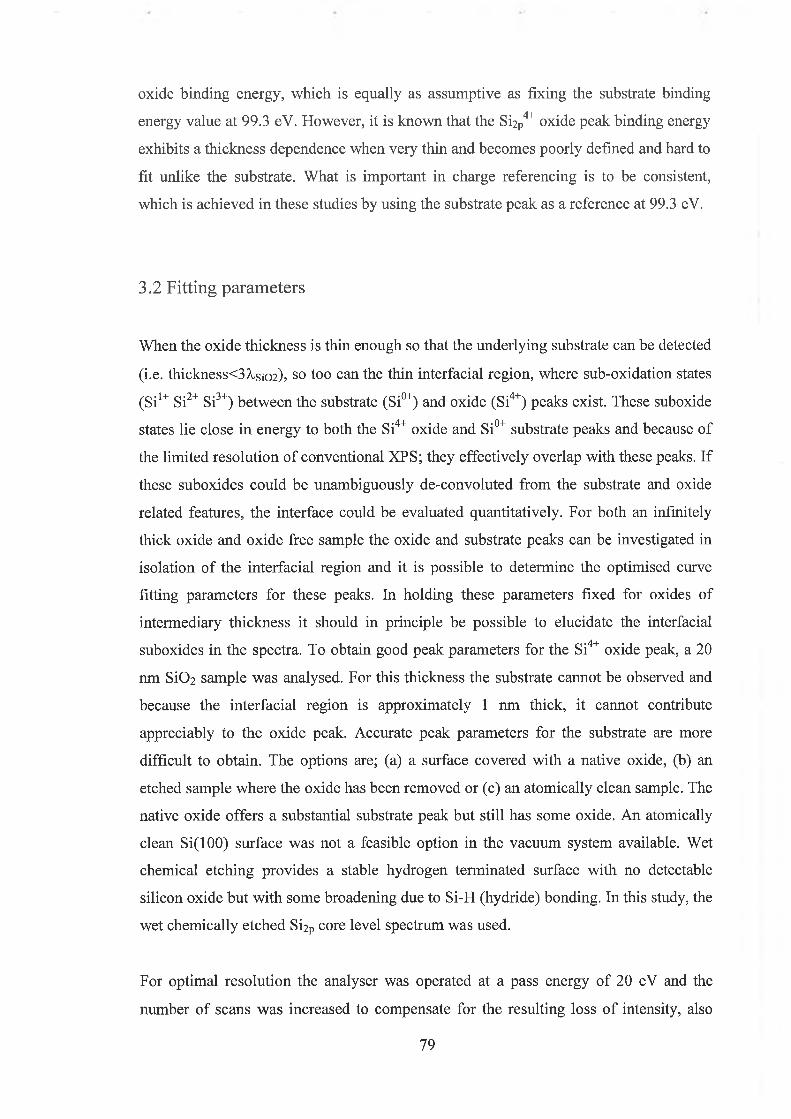
oxide b inding energy, w h ich is equally as assum ptive as fix in g the substrate binding
energy value at 99 .3 eV . H ow ever, it is know n that the S i2 P4+ ox id e peak binding energy
exhibits a th ickness dependence w hen very thin and b ecom es poorly defined and hard to
fit unlike the substrate. W hat is im portant in charge referencing is to be consistent,
w hich is ach ieved in th ese studies by u sing the substrate peak as a reference at 99.3 eV.
3.2 Fitting parameters
W hen the o x id e th ick ness is thin enough so that the underlying substrate can be detected
(i.e. th ick ness< 3 A-si0 2 ), so too can the thin interfacial region , w here sub-oxidation states
(S i1+ S i2+ S i3+) b etw een the substrate (S i0+) and ox id e (S i4+) peaks exist. T hese suboxide
states lie c lo se in energy to both the S i4+ ox id e and S i0+ substrate peaks and because o f
the lim ited reso lu tion o f conventional X PS; they e ffec tiv e ly overlap w ith these peaks. I f
these su boxid es cou ld be unam biguously de-convolu ted from the substrate and oxide
related features, the interface could be evaluated quantitatively. For both an infinitely
thick ox id e and o x id e free sam ple the ox id e and substrate peaks can be investigated in
iso lation o f the interfacial region and it is p ossib le to determ ine the optim ised curve
fitting parameters for th ese peaks. In hold ing th ese parameters fixed for oxides o f
interm ediary th ick ness it should in principle be p ossib le to elucidate the interfacial
suboxides in the spectra. To obtain good peak parameters for the S i4+ oxide peak, a 20
nm S i0 2 sam ple w a s analysed. For this th ickness the substrate cannot be observed and
because the interfacial region is approxim ately 1 nm thick, it cannot contribute
appreciably to the o x id e peak. A ccurate peak parameters for the substrate are more
d ifficu lt to obtain. T he options are; (a) a surface covered w ith a native oxide, (b) an
etched sam ple w here the ox id e has been rem oved or (c ) an atom ically clean sam ple. The
native ox id e offers a substantial substrate peak but still has som e oxide. A n atom ically
clean S i(1 0 0 ) surface w as not a feasib le option in the vacuum system available. W et
chem ical etch ing provides a stable hydrogen term inated surface w ith no detectable
silicon ox id e but w ith som e broadening due to S i-H (hydride) bonding. In this study, the
w et ch em ica lly etched S i2 P core lev e l spectrum w as used.
For optim al reso lu tion the analyser w as operated at a pass energy o f 20 eV and the
number o f scans w a s increased to com pensate for the resulting lo ss o f intensity, also
79
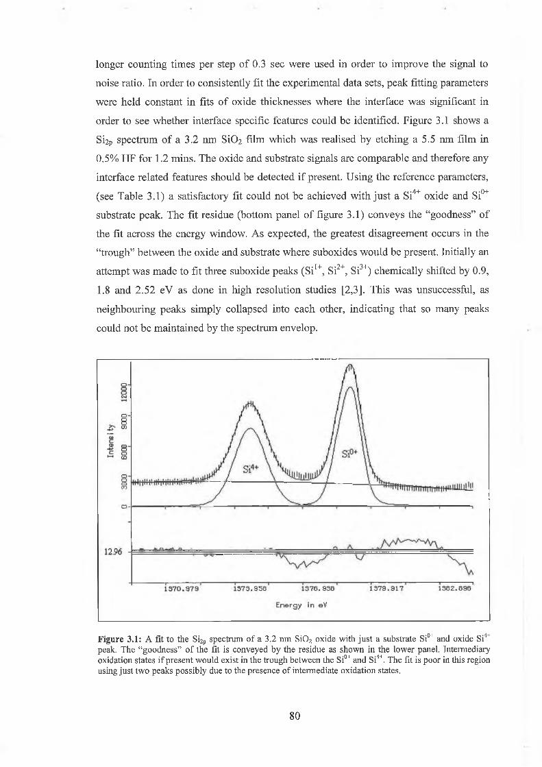
longer counting tim es per step o f 0.3 sec w ere used in order to im prove the signal to
n o ise ratio. In order to consistently fit the experim ental data sets, peak fitting parameters
w ere held constant in fits o f ox ide th icknesses w here the interface w as significant in
order to see w hether interface sp ecific features could be identified . Figure 3.1 show s a
SÍ2 P spectrum o f a 3 .2 nm SÍO 2 film w h ich w as realised by etch ing a 5.5 nm film in
0.5% H F for 1.2 m ins. T he oxide and substrate signals are com parable and therefore any
interface related features should be detected i f present. U sin g the reference parameters,
(see Table 3 .1 ) a satisfactory fit cou ld not be ach ieved w ith ju st a S i4+ oxide and S i0+
substrate peak. T he fit residue (bottom panel o f figure 3 .1) co n v ey s the “goodness” o f
the fit across the energy w indow . A s expected , the greatest d isagreem ent occurs in the
“trough” b etw een the ox id e and substrate w here suboxides w ou ld be present. Initially an
attempt w as m ade to fit three suboxide peaks (S iI+, Si2+, S i3+) ch em ica lly shifted by 0.9,
1.8 and 2 .5 2 eY as done in high resolution studies [2 ,3]. T his w as unsuccessfu l, as
neighbouring peaks sim p ly co llapsed into each other, indicating that so m any peaks
could not b e m aintained by the spectrum envelop .
Figure 3.1: A fit to the Si2p spectrum o f a 3.2 nm S i0 2 oxide with just a substrate Si0+ and oxide Si4+ peak. The “goodness” o f the fit is conveyed by the residue as shown in the lower panel. Intermediary oxidation states if present would exist in the trough between the Si0+ and Si4+. The fit is poor in this region using just two peaks possibly due to the presence of intermediate oxidation states.
80

Si4+ Sixl+ Si Siu+
Ek-E k[Siu+]eV 3.2 — - 0
FWHM 1.5 — — 0.89
Table 3.1: Si2p fit parameters for figure 3.1
N ex t the spectrum w as fitted u sing tw o suboxide peaks w ith one adjacent to the
substrate and on e to the ox ide, the expectation being that these peaks cou ld fo llo w the
em ergence o f the suboxide peaks adjacent to the m ain peaks, g iven that the m ain peak
parameters w ere held to the reference values. W hen fitted w ith ju st tw o suboxide peaks
as w e ll as a S i4+ ox id e and a S i0+ substrate peak an ex ce llen t fit w as obtained as seen in
figure 3.2 . T he fit parameters are sum m arized in table 3.2.
F igure 3.2: A fit to the Si2p spectrum o f a 3.2 nm S i0 2 oxide with two suboxide peaks. The agreement between data and fit is good across entire spectrum.
81
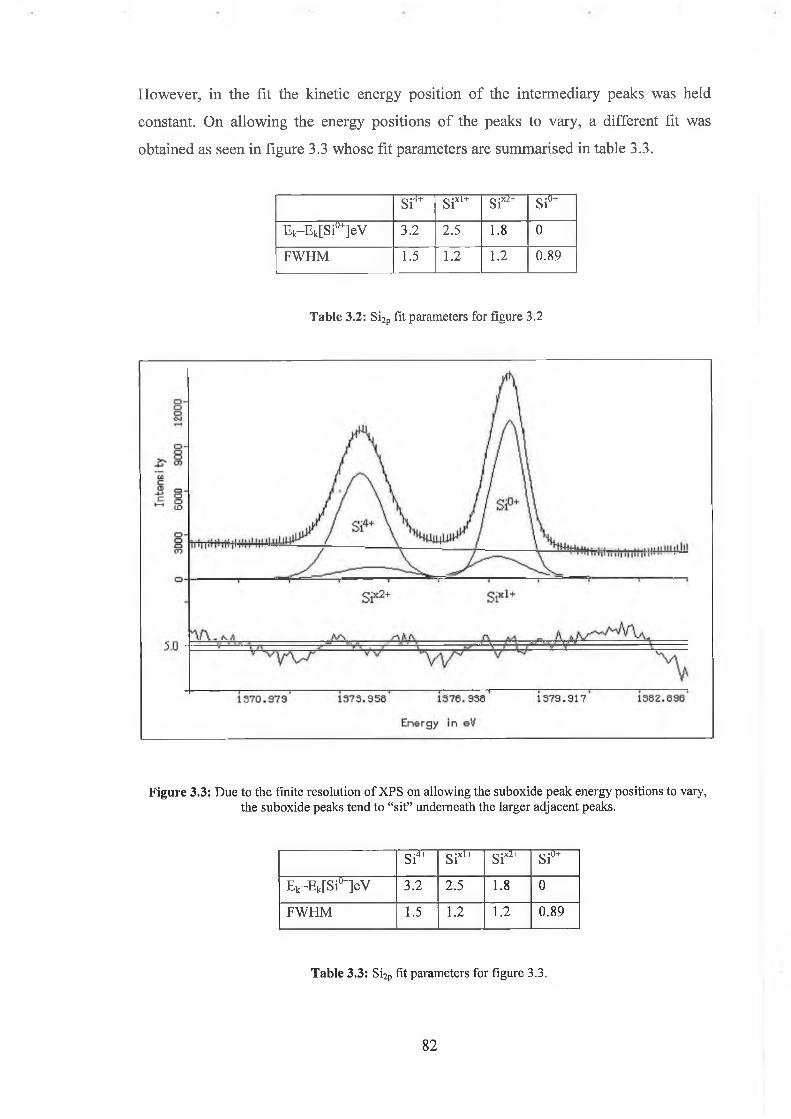
H ow ever, in the fit the kinetic energy p osition o f the interm ediary peaks w as held
constant. O n a llow in g the energy p osition s o f the peaks to vary, a different fit w as
obtained as seen in figure 3.3 w h ose fit parameters are sum m arised in table 3.3.
Si4+ Sixl+ Sixi+ Siu+
E k- E k[Si0+]eV 3.2 2.5 1 . 8 0
FW H M 1.5 1 . 2 1 . 2 0.89
Table 3.2: Si2p fit parameters for figure 3.2
F igure 3.3: Due to the finite resolution o f XPS on allowing the suboxide peak energy positions to vary, the suboxide peaks tend to “sit” underneath the larger adjacent peaks.
Si4+ Sixl+ s r 21 Siu+
Ek-E k[Siu+]eV 3.2 2.5 1 . 8 0
FWHM 1.5 1 . 2 1 . 2 0.89
Table 3.3: Si2p fit parameters for figure 3.3.
82
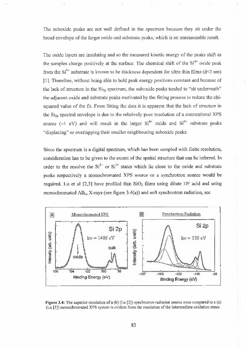
The suboxide peaks are not w ell defined in the spectrum because they sit under the
broad en velop e o f the larger ox id e and substrate peaks, w h ich is an unreasonable result.
The ox id e layers are insulating and so the m easured k inetic energy o f the peaks shift as
the sam ples charge p ositive ly at the surface. T he chem ical sh ift o f the S i4+ oxide peak
from the S i0+ substrate is know n to be th ickness dependent for ultra thin film s (d<3 nm)
[1]. Therefore, w ithout being able to hold peak energy p osition s constant and because o f
the lack o f structure in the Si^p spectrum , the suboxide peaks tended to “sit underneath”
the adjacent o x id e and substrate peaks m otivated by the fitting p rocess to reduce the chi-
squared va lu e o f the fit. From fitting the data it is apparent that the lack o f structure in
the S i2 P spectral en velop e is due to the relatively poor resolution o f a conventional X PS
source (~1 eV ) and w ill result in the larger S i4+ ox id e and S i0+ substrate peaks
“disp lacing” or overlapping their sm aller neighbouring suboxide peaks.
S ince the spectrum is a digital spectrum, w h ich has been sam pled w ith fin ite resolution,
consideration has to be g iven to the extent o f the spatial structure that can be inferred. In
order to the reso lv e the Si3+ or S i1+ states w h ich lie c lo se to the oxide and substrate
peaks resp ectively a m onochrom ated X P S source or a synchrotron source w ould be
required. L u et al [2 ,3] have profiled thin SiC>2 film s u sing dilute HF acid and using
m onochrom ated A lk a X -rays (see figure 3 .4 (a )) and soft synchrotron radiation, see
|A] M onochr ornate d XPS
Binding Energy [eV)
Synchrotron Radiation
-95
Binding Energy (eV)
F igure 3.4: The superior resolution o f a (b) (Lu [2]) synchrotron radiation source even compared to a (a) (Lu [3]) monochromated XPS system is evident from the resolution o f the intermediate oxidation states.
83
figure 3 .4(b) and have succeeded in d e-con volv in g the S i2 P spectra into the constituent
oxidation states. In figure 3 .4(a), the ox id e th ickness is 6 .4 nm thick. The oxide
th ickness is not reported for the spectrum in figure 3 .4 (b ) but considering the photon
energy is 130 eV the th ickness is estim ated to be b etw een 0 .9 and 0 .14 nm. The
d ifficu lties o f de-convolu ting the interfacial signal from the ox id e has m eant that in
m ost X P S studies no attempt has been m ade to d e-convolu te the interfacial signal from
the ox ide. Rather, the em phasis has been on film th ickness [2 ],[4 ], stoichiom etry [5,6]
and elem ental com position .
The u ltim ate goal o f quantitatively assessin g the interface it seem s is a “ bridge too far ”
w h ich cannot be spanned w ith the degree o f surface sen sitiv ity and resolution
capabilities o f a conventional X P S source. H ow ever, m otivated by the h igh quality o f
the dielectric, a qualitative interpretation o f the interface w as pursued in this thesis by
a llow ing the FW H M o f the ox id e and substrate to vary freely and fitting a single
suboxide peak w ith a fixed FW H M o f 1.7 eV , w h ich w as a llow ed to vary in position.
The ob jective o f the study w as to g iv e indication o f the em ergence o f the interface states
by co n v ey in g approxim ately the energy p osition o f the su boxid es and any changes in
the F W H M o f the s ilico n in the substrate or in the bulk ox id e layer.
N o su boxid e peak cou ld be fitted in the as-received spectra. E v en for the thinnest oxide
(5 .5 nm ), no interfacial suboxide peak could be detected w h ich w as attributed to the fact
that the sm all interfacial signal w as being attenuated by the overly ing oxide. It w as
necessary therefore to thin the oxide in order to determ ine w hether interfacial sub
o x id es cou ld be detected. A s m entioned previously , tw o approaches w ere used to
rem ove the bulk o f the overlying ox id e layer, argon bom bardm ent and w eak HF acid
etching.
3.3 Ar ion Bombardment
D ue to their fu ll outer sh ells and large atom ic num ber argon atom s are inert and
relatively h eavy (Z =18). W hen ion ised in an electron discharge they can be accelerated
under the in fluence o f an applied electric fie ld and crashed into a sam ple surface thus
rem oving som e o f the outer surface atom s. For sam ple c lean in g purposes this is usefu l
84
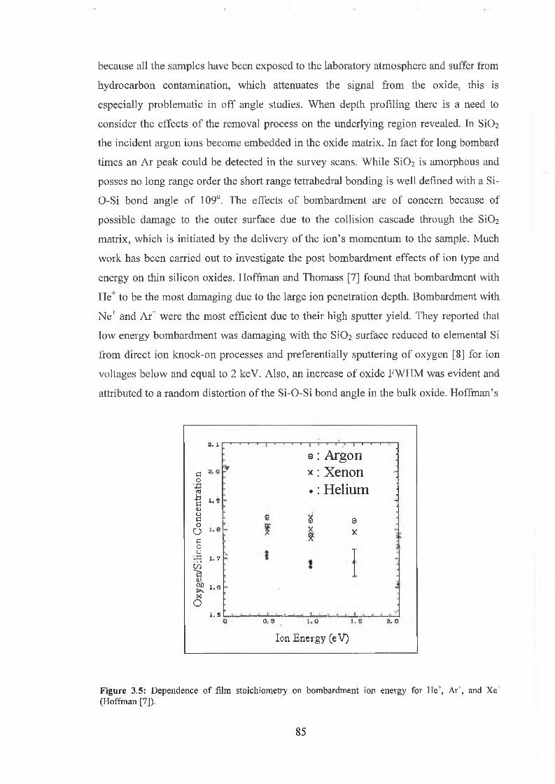
because all the sam ples have been exp osed to the laboratory atm osphere and suffer from
hydrocarbon contam ination, w h ich attenuates the signal from the oxide, this is
esp ecia lly problem atic in o f f angle studies. W hen depth p rofiling there is a need to
consider the effects o f the rem oval process on the underlying region revealed. In SiC>2
the incident argon ions b ecom e em bedded in the ox id e matrix. In fact for long bombard
tim es an A r peak cou ld be detected in the survey scans. W h ile SiC>2 is amorphous and
p osses no long range order the short range tetrahedral bonding is w e ll defined w ith a Si-
O -Si bond angle o f 109°. The effects o f bom bardm ent are o f concern because o f
p ossib le dam age to the outer surface due to the co llis io n cascade through the SiC>2
matrix, w h ich is initiated by the delivery o f the io n ’s m om entum to the sam ple. M uch
w ork has been carried out to investigate the p ost bom bardm ent effec ts o f ion type and
energy on thin s ilico n oxides. H offm an and T hom ass [7] found that bombardment with
H e+ to be the m ost dam aging due to the large ion penetration depth. Bom bardm ent w ith
N e + and A r+ w ere the m ost efficien t due to their h igh sputter y ield . They reported that
lo w energy bom bardm ent w as dam aging w ith the S i0 2 surface reduced to elem ental Si
from direct ion k nock-on processes and preferentially sputtering o f oxy g en [8 ] for ion
voltages b e lo w and equal to 2 keV . A lso , an increase o f ox id e FW H M w as evident and
attributed to a random distortion o f the S i-O -S i bond angle in the bulk oxide. H offm an’s
3. 1 I ' ‘—i-
£Ocd£5=1QJOS=!OOS=JoCJ
• 1—f 0 0
<DGOh-K>No
1 . 9
1, 7
I. a
J . . S
0: Argon x : Xenon ♦: Helium
0 , 3
sX
Ion Energy (eV )
Figure 3.5: Dependence o f film stoichiometry on bombardment ion energy for He+, Ar+, and Xe+ (Hoffman [7]).
85

th ickness estim ate o f the reduced s ilico n region w as 0 .4 nm and so he reasoned that he
cou ldn ’t detect elem ental Si associated w ith it g iven the large sam pling depth o f X PS.
Instead, he carefu lly m onitored the film stoichiom etry (see figure 3 .5 ) having corrected
for carbon contam ination and attributed the sub-stoich iom etric va lues to an outer layer
w here o x y g en had b een preferentially sputtered leav in g a s ilico n rich elem ental region.
Other w orkers have also reported that the surface o f a bom barded S i0 2 film contained
reduced s ilico n o x id es [9 ],[11]. H ow ever, there is d isagreem ent about the effects o f
bom bardm ent, w ith a recent study b y Benkherourou and D e v ille [11] using both H e and
Ar ions sh ow ing no indication o f surface reduction as ev id en ced by a constant S i:0
stoichiom etry and O is to S i2 P energy difference. Surprisingly they found that the O is and
Si2 P peak F W H M s w ere also unchanged, indicating that no dam age to the S i-O -Si bond
angle w as introduced. Paparazzo [12-13] et al have undertaken exten sive studies o f the
effects o f ion bom bardm ent on S i0 2 . H ow ever, before considering their findings it is
usefu l to consider the results o f a round robin study lead by H ashim oto et al [14] who
classified o x id es by the change in chem ical state caused by sputtering using tw o
parameters: the change in free form ation enthalpy (arising from thermal reduction o f
oxides) and the ion icity .
Enthalpy:
Is a state function in therm odynam ics and is defined as the heat absorbed by a system at
constant pressure. T he oxidation o f silicon , w h ich is perform ed at constant pressure and
temperature, is exotherm ic (the system surrenders heat to it ’s surroundings) and thus
results in a n egative enthalpy change. T he enthalpy change o f form ation is a measure o f
the stability o f a com pound form ed from its reactants. For exam ple a p iece o f w ood
w hen burned g iv es o f f heat, the final state, carbon is m uch m ore stable than the original
w ood state, the enthalpy change is negative.
I f the ox idation p rocess is v iew ed as on e w here the S i0 2 system is h igh ly perturbed and
the enthalpy o f reactants (S i and O) is com pared to that o f the product (S i0 2 ). W hich is
m ore stable? W hat w ill the system do? From a p h ysics p erceptive one expects the
system to tend to a m in im um energy, but from a therm odynam ics perspective
consideration m u st b e g iven to entropy (a m easure o f the disorder o f the system ).
86

Energy:
A ball rolls dow n a h ill until it’s potential energy reaches a m in im um at the bottom. For
reactions at constant pressure (i.e. w here the system does no w ork) the change in energy
(internal energy) equals the change in enthalpy. So ju st like the ball, in exotherm ic
reactions the system lo sses heat until the total enthalpy reaches a m in im um.
Entropy:
The spontaneous m ix in g o f tw o different separated gases at the sam e pressure can occur
w ithout a change in energy but results in a m ore random dispersal o f the total energy, or
an increase the disorder. In an endotherm ic reaction the system can gain energy and still
proceed spontaneously , here the entropy dom inates.
B oth enthalpy and entropy terms are balanced in the G ibbs equation:
A G = A H — T A S Equation 3.0
AG Is the free energy change o f a reaction system
AH Is the enthalpy change
AS Is the change in entropy
T Is temperature
H ashim oto’s perceptive is unconventional, as ordinarily the stability o f form ation o f a
com pound from it constituents is considered. W ater form ation for exam ple results in a
n egative enthalpy as the final state is m ore stable than the initial.
2 H 2 (g a s)+ 0 2 (gas) —> 2 H 2 0 (liq u id )
I f considered in reverse then the enthalpy change w ou ld be p ositive in order to convey
the sam e result. H ashim oto is not considering oxidation but rather reduction. A lso , the
u se o f therm al reduction is m islead ing as he is referring to the “therm al vibration “ or
perturbation arising from the bombardment process. This exp lains the signs o f the
enthalpy ch an ges su ggested by him b e lo w in c lassify in g ox id es in term s o f whether or
not they w ill be reduced w hen bom barded in term s o f their ion ic ity and enthalpy
change.
87
Ion icity>0.5 and AHa> 0 The ox id e d oesn ’t change.
Ion icity<0.5 and AHa> 0 The ox id e is dam aged but not reduced.
AHa<0 The ox id e w as reduced and n ew com ponents appear.
S in ce temperature is a lw ays p ositive on the absolute scale, w hen a reaction occurs at
constant temperature and pressure the free energy o f the system decreases. H ashim oto is
effec tiv e ly saying that SiC>2 is u n likely to d isassociate into suboxides w hen high ly
excited as that w ou ld correspond to an increase in G ibbs energy (equation 3.0). Other
o x id es like TaOs or T i0 2 for exam ple w h ose free form ation enthalpy change is negative
are reduced during bom bardm ent as the constituent parts state is m ore stable than the
final oxide.
T he role o f ion ic ity is seen g iven that the effects o f bom bardm ent for lo w energy (E<3
k eV ) ions is to disrupt the so lid to a depth o f around 10 nm b e lo w the surface [15]. The
local vibration o f atom s can d isp lace them from their m ean position s. For oxides w ith a
large ion icity the disturbed atom s can recover their original position s due to the long-
range cou lom b interaction o f the recoiled atom s, w here as for ox id es w ith lo w ionicity
the atom s m ay stab ilize at p osition s different from their original ones and such oxides
are dam aged.
S i0 2 has a p o sitiv e enthalpy change and an ion icity b e lo w 0 .5 and so from H ashim oto’s
p erspective a reduction o f the surface is not expected , but lattice dam age v ia S i-O -Si
bond angle random isations resulting in a peak FW H M increase is reasonable.
H ash im oto’s approach is sim ple and usefu l but fa ils to anticipate an outer reduced oxide
region in S i0 2 . Specu latively , the reason m ay ex ist in the deliverance o f the ion energy
to the outer surface. In laser ablations experim ents w here intense energy is delivered in
short p u lses to the outer region w here the energy absorbed cannot be conducted away
quickly enough and so the outer surface ex ists in a h igh ly excited state and is ablated.
A n alogou sly it is p ossib le that the outer region o f the o x id e absorbs the im pact o f the
incident ions, the im pulse imparted is felt loca lly to the extent that a surface localised
“dam age region ” ex ist w here o x y g en is preferentially sputtered. T he “shock” o f the
incident ion flu x is transm itted b elo w this region and it is here that H ashim oto’s
8 8
form alism is va lid w ith a disp laced oxy g en being recovered and the co llis ion cascade
initiated at the surface effecting on ly the peak FW H M . It is interesting to consider, h ow
th ick the dam age zon e is. Is it on the order o f the ion penetration depth? D oes it depend
on the ion energy? Can it be detect w ith X PS?
A t h igh accelerating vo ltages (~5 k eV ) Paparazzo et al [12] have considered the
evo lu tion o f the s ilico n and oxy g en A uger parameters a* w h ich are defined as:
a ‘Si = E k (S iK L L )+ E b (S i2p )
a * 0 = E k (O K V V ) + E b (O ls)
w here Ek(Si K LL) and E k (0 K V V ) are the kinetic energies o f the silicon and oxygen
induced A uger transitions respectively , Eb(Si 2p) and E b (0 Is) are the silicon 2p and
o xygen Is b inding energies respectively . (Note: C onventionally the d ifference betw een
Ek and Eb is considered but here the sum is used in order to a lw ays obtain positive
values [16]). Investigating the effec t o f ion energy on the chem ical state o f the S i0 2
film s Paparazzo et al [12] found that for energies above 5 k eV the surface is reduced
w ith the introduction n ew surface SiO x com ponents in the A uger parameters. T hese
w ere due to the lo ss o f surface o x y g en and the subsequent S i-S i recom bination o f
truncated S i- 0 bonds. T he m erits o f the S iL V V spectra in detecting these n ew artefacts
arises from it ’s ab ility to fo llo w differences b etw een S i-S i and S i- 0 bonding states as
th is auger peak in v o lv es transitions (to both continuum and discrete states) o f valence
electrons.
For ion energies in the range 1 to 2 .5 keV Paparazzo found virtually no evidence o f
dam age u sing the X P S S i2 P and SiKLL peaks. B ut for the sam e bombardment
conditions, dam age w as detected in surface sen sitive synchrotron radiation studies [16],
lead ing Paparazzo to the conclude that SiO x dam age is detectable on ly w hen the
attenuation length o f the probing photoelectron is com parable to the dam age depth
w h ich in turn is related to the io n energy and m ass. T his is a reasonable result w hen one
considers that a 0.4 to 0.8 nm dam age region (for 2 k eV ions) is n eg lig ib le in thickness
com pared to the 7-10 nm sam pling depth typ ically found in X P S (Ek>1380 eV ), but
com parable to the 1 nm sam pling depth o f 130 eV synchrotron radiation (Ek~30 eV ).
89

Paparazzo further concluded that the FW H M increase arises from a random re-ordering
o f the S i-O -S i bond angle and bom bardm ent induced surface roughening.
The effect o f bom bardm ent tim e (for 2 k eV ions) on peak FW H M observed by
Paparazzo is sh ow n in figure 3 .6 . H e reported that both O ls and O K V V peak FW H M
behaved in the sam e w ay as the Si4+ ox id e and SiK L 2 3 L 2 3 .
Figure 3.6: FW HM values o f Si2p and X-ray induced Si KL23L23 signals o f the oxidised components o f silicon in the S i0 2/Si system as a function o f the 2 keV Ar+ etch time. (Paparazzo [12])
Figure 3 .7 sh ow s the evo lu tion o f both the Si2 P and O is spectra o f a 13.4 nm S i0 2 oxide
after su ccessiv e bom bardm ents at 2 keV . Show n are the fitted peaks w ithout the raw
data or experim ental fit, w ith background rem oved and charge referenced to the Si2 P0+
substrate peak at 99 .3 eV .
N ote: The o m issio n o f raw and fitted data in figure 3 .7 is unconventional. The presence
o f both ordinarily a llo w s one to assess the “good n ess” o f the fit. H ow ever, the aim was
to sh ow the evo lu tion o f peak position and FW H M w ith th ickness, w hich is best done
w ith all spectra p lotted in the sam e w indow . W ith the k inetic energy o f the suboxide
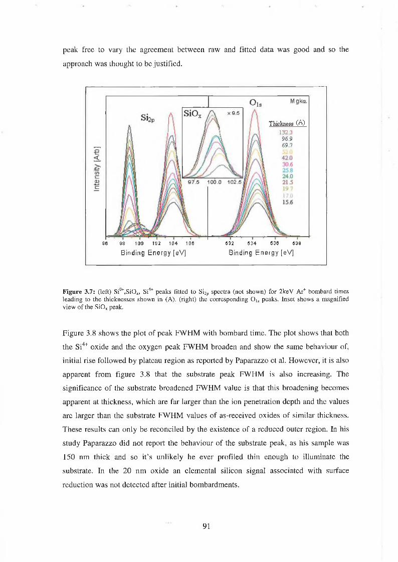
peak free to vary the agreem ent betw een raw and fitted data w as good and so the
approach w as thought to be justified .
96 98 100 102 104 106
B in d i n g E n e r g y [eV]
532 5 3 4 536 538
B ind in g E n e r g y [eV]
Thickness (f~0132.396.969.7
F igure 3.7: (left) Si0+,SiOx, Si4+ peaks fitted to Si2p spectra (not shown) for 2keV Ar+ bombard times leading to the thicknesses shown in (A), (right) the corresponding Ois peaks. Inset shows a magnified view of the SiOx peak.
Figure 3.8 sh ow s the p lot o f peak FW H M with bombard tim e. T he plot show s that both
the S i4+ ox id e and the oxygen peak F W H M broaden and show the sam e behaviour of,
initial rise fo llo w ed by plateau region as reported by Paparazzo et al. H ow ever, it is also
apparent from figure 3 .8 that the substrate peak FW H M is also increasing. The
sign ifican ce o f the substrate broadened FW H M value is that this broadening becom es
apparent at th ickness, w hich are far larger than the ion penetration depth and the values
are larger than the substrate FW H M values o f as-received ox ides o f similar thickness.
T hese results can on ly be reconciled by the ex istence o f a reduced outer region. In his
study Paparazzo did not report the behaviour o f the substrate peak, as his sam ple was
150 nm thick and so it’s u n likely he ever profiled thin enough to illum inate the
substrate. In the 20 nm ox id e an elem ental silicon signal associated with surface
reduction w as not detected after initial bombardments.
91

Figure 3.8: Plot of Si2p0+,Si2p4+ and Ois peak FWHM with bombard time. The FWHM behaviour is similar to that o f figure 3.6. The increase in the Si0+ FWHM is unexpected however, and may arise for surface species.
If P aparazzo’s argum ent in relation to the extent o f the dam age region being much
sm aller than the sam pling depth is accepted then this finding is not unreasonable. Its
interesting to consider i f the substrate FW H M when detected after the overlying oxide
has been bom barded to a th ickness com parable to the sam pling depth, can reveal the
presence o f the thin reduced dam age region through the increased contribution to the
substrate peak FW H M from the reduced region. T able 3 .4 sum m arizes the peak
parameters obtained in bom barding the 13.4 nm oxide.
92
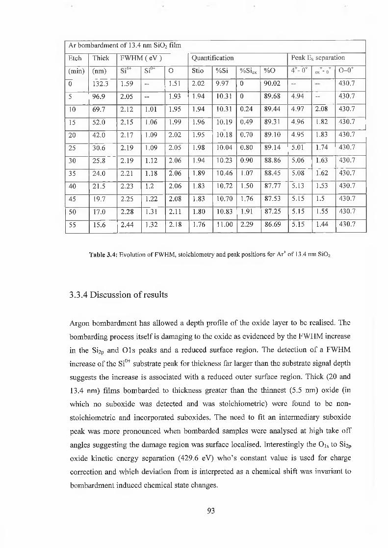
A r bom bardm en t o f 13.4 nm S i0 2 film
E tch T hick F W H M ( eV ) Q uan tification P eak Ek separation
(m in) (nm )
+
S i0+ O Stio % Si % S i0X %o+o1+ + +
ox - 0 o-o+0 132.3 1.59 — 1.51 2.02 9.97 0 90.02 - 430.7
5 96.9 2.05 - - 1.93 1.94 10.31 0 89.68 4.94 — 430.7
10 69.7 2.12 1.01 1.95 1.94 10.31 0.24 89.44 4.97 2.08 430.7
15 52.0 2.15 1.06 1.99 1.96 10.19 0.49 89.31 4.96 1.82 430.7
20 42.0 2.17 1.09 2.02 1.95 10.18 0.70 89.10 4.95 1.83 430.7
25 30.6 2 .19 1.09 2.05 1.98 10.04 0.80 89.14 5.01 1.74 430.7
30 25.8 2.19 1.12 2.06 1.94 10.23 0.90 88.86 5.06 1.63 430.7
35 24.0 2.21 1.18 2.06 1.89 10.46 1.07 88.45 5.08 1.62 430.7
40 21.5 2.23 1.2 2.06 1.83 10.72 1.50 87.77 5.13 1.53 430.7
45 19.7 2.25 1.22 2.08 1.83 10.70 1.76 87.53 5.15 1.5 430.7
50 17.0 2.28 1.31 2.11 1.80 10.83 1.91 87.25 5.15 1.55 430.7
55 15.6 2.44 1.32 2.18 1.76 1 1 . 0 0 2.29 86.69 5.15 1.44 430.7
Table 3.4: Evolution of FWHM, stoichiometry and peak positions for Ar+ o f 13.4 nm S i0 2
3.3.4 Discussion o f results
A rgon bom bardm ent has a llow ed a depth profile o f the ox id e layer to be realised. The
bom barding p rocess its e lf is dam aging to the ox id e as ev id en ced by the FW H M increase
in the S i2 P and O ls peaks and a reduced surface region. The detection o f a FW H M
increase o f the S i0+ substrate peak for th ickness far larger than the substrate signal depth
suggests the increase is associated w ith a reduced outer surface region. Thick (20 and
13.4 nm ) film s bom barded to th ickness greater than the th innest (5 .5 nm ) oxide (in
w h ich no su boxid e w as detected and w as stoich iom etric) w ere found to be non-
stoich iom etric and incorporated suboxides. The need to fit an interm ediary suboxide
peak w as m ore pronounced w hen bom barded sam ples w ere analysed at h igh take o f f
angles su ggestin g th e dam age region w as surface localised . Interestingly the O is to Siap
oxid e k inetic energy separation (429 .6 eV ) w h o ’s constant va lu e is u sed for charge
correction and w h ich deviation from is interpreted as a ch em ical shift w as invariant to
bom bardm ent induced chem ical state changes.
93
W e obtained a larger value o f (430 .7 eV ), and the ox id e Si4+ peak to substrate S i0+ peak
energy separation increased w ith bom bardm ent tim e. In attem pting to lim it the peak
parameters it w as acknow ledged that the peak parameters w ere ev o lv in g legitim ately. In
other w ords after each bom bardm ent a different film w as b eing “illum inated”, in the
sense that it has b een dam aged to a different extent and to a n ew depth. There w as no
prior k n ow led ge o f h o w it should behave “exactly” and so it w as a llow ed to “speak
freely” by leav in g it’s parameters unconstrained.
The suboxide peak chem ical shift (relative to the silicon substrate S i0+) and intensity
behaviour w a s the sam e for sam ples w here the substrate cou ld and could not be
detected. It d isp layed an initial shift o f approxim ately 2.1 eV from the S i0+ peak and
m oved p rogressive ly closer to the substrate as the ox id e w as thinned.
A s a m eans to better illum inate the interface by rem oving the bulk o f the overlying
oxide, argon io n bom bardm ent appears to have to o m any drawbacks. H aving to “look
through” a dam aged ox id e and surface suboxides, it is very d ifficu lt to distinguish
betw een interfacial and surface suboxides in an unam biguous w ay. In this thesis, the
detection and inferrel o f a reduced surface reg ion is uncertain, and questioned by the
m ore ex ten siv e w ork o f Paparazzo et al. N on eth eless ours w as not the pursuit o f ion
bom bardm ent induced effects on SiC>2 but rather the su itability o f bom bardm ent as a
profile m echanism , to this end it’s unfeasibility has b een ascertained because the
introduction o f suboxides by the bom bardm ent process m akes it im possib le to
determ ine w h ich signal originates from suboxide sp ecies present prior to bombardment.
3.4 S i02 Chemical depth profile using weak HF etching
D epth profiles o f the 5.5 nm S i0 2 ox id e w ere realised by im m ersion for su ccessive ly
longer tim es in d ilute (0.5% ) HF acid. A t this HF concentration an average etch rate o f
1.9 nm per m inute w as obtained. N o surface pre-treatm ent w as perform ed; the sam ples
w ere im m ersed as-received . The etch w as term inated by the addition o f a large quantity
o f deion ised w ater to the etching solution. Prior to the sam ple introduction into the X PS
instrument, the sam ple w as b low n dry w ith nitrogen and inserted into the vacuum
system load lo ck as qu ick ly as possib le.
94

In this w ay the etched surface w as exp osed to the laboratory atm osphere on ly for the
tim e taken to dry and insert it, w hich is less than 10 min. E very effort w as made to
achieve reproducibility and con sisten cy in the etch ing procedure so as to m inim ise
sam ple d ifferences arising from d ifferences in etch tim e, rinse tim e or involuntary
contam ination. Figure 3 .9 sh ow s the S i2 P spectrum o f 5.5 nm SiC>2 film s etched for 2 .0
tnins in 0.5% H F solution.
Kine t i c e n e r g y [eV ]
Figure 3.9: An unknown contribution to the Si2p spectrum of an etched oxide due to surface contamination, shown in red. An identical sample without contamination is shown in black.
O ne sam ple w as contam inated by fa llin g onto its face and is represented by the red
spectrum. Show n in b lack is the spectrum o f an un-contam inated ox id e etched for the
sam e time. In figure 3 .9 the reproducibility o f the ox id e and substrate peak intensities is
extrem ely good. H ow ever, an additional feature is evident on the high kinetic energy
side o f the substrate peak, w hich cannot be identified and indicates the precautions,
w hich must be fo llo w ed in sam ple handling.
95
3.4.1 Quantification concerns
A k ey parameter in a S i0 2 film depth profile is the ratio o f the S i4+ oxide to oxygen
peak intensity as it reflects the stoichiom etric com position o f the layer. W hile this ratio
d o esn ’t sh ow the ox ide stoich iom etry directly, because there is the need to correct for
sensitiv ity factors. B ut th ese factors are constant values. T he poin t is that the absolute
stoichiom etry value is not important but rather its evo lu tion w ith depth; this evolution is
enshrined in the o x y g en to ox id e ratio. For sam ple th ickness less than 5.5 nm, the f ilm
stoichiom etry w as consisten tly seen to increase above a va lue o f 2 . 0 as the layer w as
thinned. The extent o f the increase w as less pronounced for the Ar bombarded sam ples.
It is m ost lik e ly that the film s are in fact stoichiom etric (0 /S i= 2 .0 ) and tend to a sub-
stoichiom etric (0 /S i< 2 .0 ) value as expected at lo w ox id e th ickness but the com bined
effec ts of; “freedom ” o f peak FW H M , increased in fluence o f surface contam ination and
interfacial su boxid e regions “conspire” to underm ine the reliability o f the quantification
analysis at sm all ox id e thickness.
Q uantitative analysis is concerned w ith the concentration o f different elem ents in the
sam ple. The sam ple is assum ed to be h om ogen eou s w ith each elem ent uniform ly
distributed w ith depth. Shallenberger et al [20] as d iscussed b e lo w addresses the special
quantification d ifficu lties in ox id es arising from a non-uniform nitrogen distribution
w ith its surface signal exaggerated and interfacial signal underestim ated. H e points out
the role o f surface hydrocarbon in attenuating the underlying ox id e and substrate signal.
For both s ilico n d iox id e and oxynitride film s, surface contam ination, although thin,
form s a larger fraction o f the overall film th ickness as the film is thinned. So does the
interfacial suboxide region w h o ’s signal is m ore pronounced as the attenuating
overlying o x id e is thinned. A lso in the context o f Grunthaner’s [21] w ork w e are
m indful o f the p ossib ility o f a strained stoichiom etric SiC>2 region sandw iched betw een
the su boxid e reg ion and the bulk oxide, its presence w ou ld b ecom e m ore significant
w ith thinning.
97
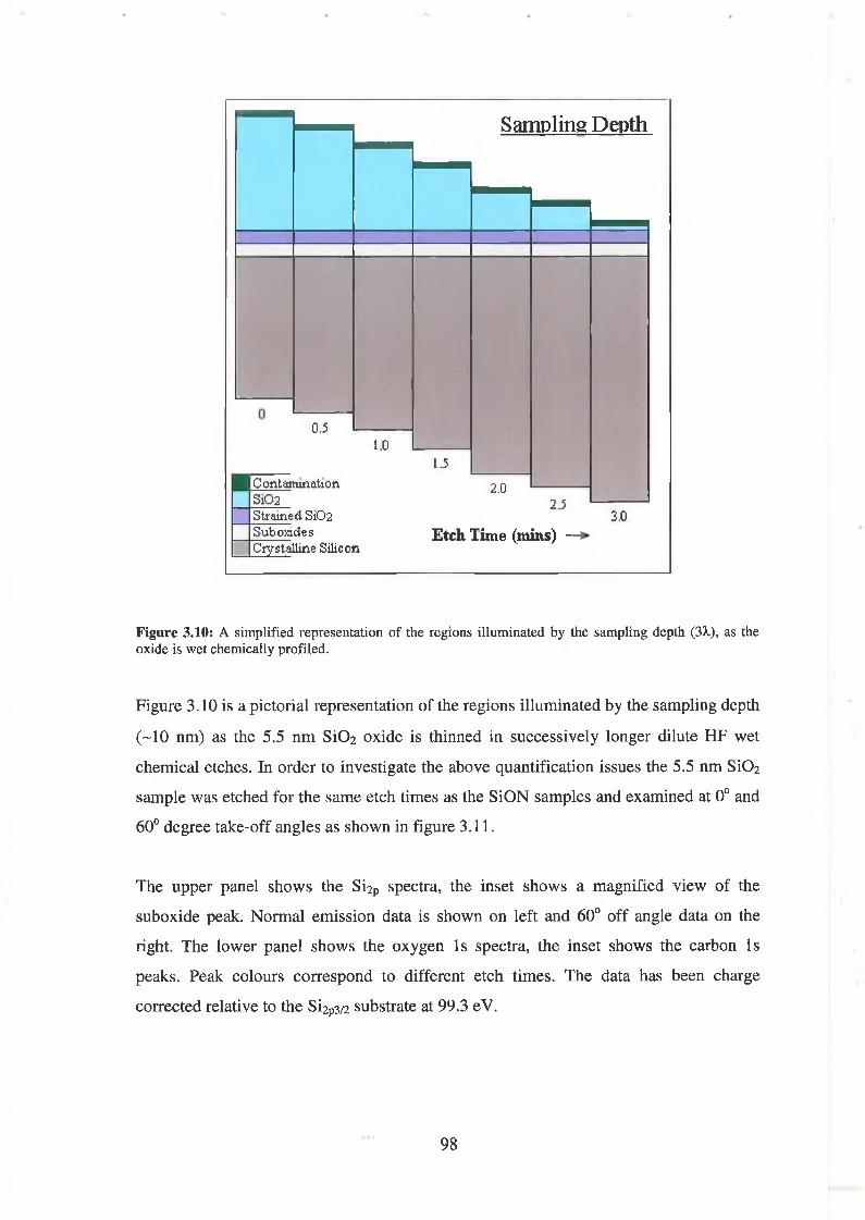
Sampling Depth
0.5
I ContaminationS1O2Strained S1O2Suboxides
1.0
Crystalline Silicon
1.5
2.075
Etch Time (mins) -3.0
Figure 3.10: A simplified representation of the regions illuminated by the sampling depth (3A,), as the oxide is wet chemically profiled.
Figure 3 .1 0 is a pictorial representation o f the regions illum inated by the sam pling depth
( - 1 0 nm ) as the 5 .5 nm SiC>2 ox id e is thinned in su ccessiv e ly longer dilute H F w et
chem ical etches. In order to investigate the above quantification issues the 5.5 nm S i0 2
sam ple w as etched for the sam e etch tim es as the S iO N sam ples and exam ined at 0° and
60° degree tak e-off angles as show n in figure 3 .11.
T he upper panel sh ow s the S i2 P spectra, the inset sh ow s a m agnified v iew o f the
suboxide peak. N orm al em ission data is show n on left and 60° o f f angle data on the
right. The low er panel sh ow s the o xygen Is spectra, the inset sh ow s the carbon Is
peaks. Peak colours correspond to different etch tim es. T he data has been charge
corrected relative to the S i2 P3 / 2 substrate at 99.3 eV .
98

Binding Energy [eV] Binding Energy [eV]
Figure 3.11: Evolution of Sip, 0 , s and C ,s peaks of a 5.5nm S i0 2 film with dilute wet chemical HF etch time at 0° and 60° take-off angle. The fitted peaks only are shown for clarity.
The 0° and 60° degree take o ff data are plotted on the sam e intensity scales and obtained
from the sam e sam ple for each etch. Table 3.5 sum m arizes the peak parameters for the
data at 0° take o f f angle. There are a number o f key observations from figure 3.11 and
table 3.5. A reduced absolute intensity is evident at a higher tak e-off angle in all spectra
excep t for the carbon peak, w hich is enhanced. This is reasonable as the carbon signal
originates from the outerm ost region (the contam ination layer) whereas the other signals
originate from underneath the contam ination and so at grazing incidence the O is and
S i2P signals travel through a thicker effec tive contam ination layer and are thus
attenuated m ore w h ile C js signal is enhanced.
99
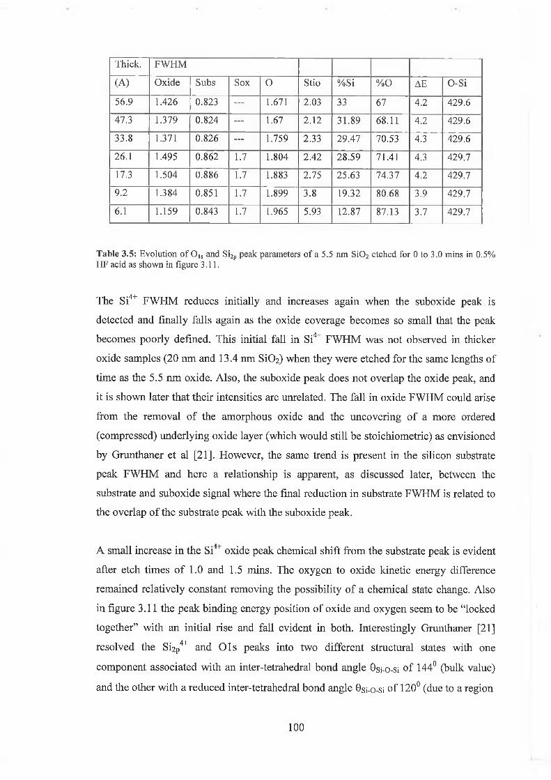
Thick. F W H M
(A) O xide Subs Sox O Stio % Si % 0 AE O -Si
56.9 1.426 0.823 — 1.671 2.03 33 67 4.2 429.6
47.3 1.379 0.824 — 1.67 2.12 31.89 68.11 4.2 429.6
33.8 1.371 0.826 — 1.759 2.33 29.47 70.53 4.3 429.6
26.1 1.495 0.862 1.7 1.804 2.42 28.59 71.41 4.3 429.7
17.3 1.504 0.886 1.7 1.883 2.75 25.63 74.37 4.2 429.7
9.2 1.384 0.851 1.7 1.899 3.8 19.32 80.68 3.9 429.7
6.1 1.159 0.843 1.7 1.965 5.93 12.87 87.13 3.7 429.7
Table 3.5: Evolution o f O l8 and Si2p peak parameters o f a 5.5 nm S i0 2 etched for 0 to 3.0 mins in 0.5% HF acid as shown in figure 3.11.
The S i4+ F W H M reduces in itia lly and increases again w h en the suboxide peak is
detected and fin a lly fa lls again as the oxide coverage b ecom es so sm all that the peak
b ecom es poorly defined . T his initial fall in S i4+ F W H M w as not observed in thicker
oxide sam ples ( 2 0 nm and 13.4 nm SiCh) w hen they w ere etched for the sam e lengths o f
tim e as the 5.5 nm oxide. A lso , the suboxide peak does not overlap the oxide peak, and
it is sh ow n later that their intensities are unrelated. The fa ll in ox id e FW H M could arise
from the rem oval o f the am orphous oxide and the uncovering o f a m ore ordered
(com pressed) underlying ox id e layer (w hich w ou ld still be stoichiom etric) as envisioned
by Grunthaner et al [21]. H ow ever, the sam e trend is present in the silicon substrate
peak FW H M and here a relationship is apparent, as d iscussed later, betw een the
substrate and su boxid e signal w here the final reduction in substrate FW H M is related to
the overlap o f the substrate peak w ith the suboxide peak.
A sm all increase in the S i4+ oxide peak chem ical sh ift from the substrate peak is evident
after etch tim es o f 1.0 and 1.5 m ins. The o xygen to ox id e k inetic energy difference
rem ained rela tively constant rem oving the p ossib ility o f a chem ical state change. A lso
in figure 3.11 the peak b inding energy position o f ox id e and o xygen seem to be “locked
together” w ith an in itial rise and fall evident in both. Interestingly Grunthaner [21]
resolved the Si2 P4+ and O ls peaks into tw o d ifferent structural states w ith one
com ponent associated w ith an inter-tetrahedral bond angle 0si-o-si o f 144° (bulk value)
and the other w ith a reduced inter-tetrahedral bond angle 0 si-o-si o f 1 2 0 ° (due to a region
100
o f com pressed SÍO 2 above the S iO x region). A n assum ption in th is de-convolution is
that the energy p osition s o f these peaks in the Si4+ ox id e and O is peak be mirror im ages
o f each other as the ch em ical shift is due to structural changes SICT not chem ical.
T he s ilico n -o x y g en stoichiom etry increases as the film is thinned; this is unexpected as
the film is expected to be stoichiom etric (S i:0 1:2) until the suboxide (S iO x) region. The
film stoichiom etry is calculated using the ox id e and o x y g en peak areas. After all the
Si4+ ox id e peak is ex c lu siv e ly associated w ith silicon bonded to four oxygen s, how ever,
the o x y g en peak has contributions from the contam ination and suboxide layers w hich
both constitute a larger fraction o f the oxygen intensity w ith reduced oxide thickness.
The problem is com pounded as the ox id e peak shifts closer to the substrate due to im age
charge effects from the substrate and becom es poorly defined as the ox id e is thinned.
A n increase in carbon and o xygen peak intensity is ev ident in figure 3.11 after the
sam ple has been etched for 0.5 m in (green peak) in the 60° ta k e-o ff angle spectra, yet
the corresponding ox id e and oxy g en spectra in the norm al angle spectra sh ow the
expected decrease w ith th ickness. It is reasonable that m any o f the carbon bonds in the
contam ination layer are o x y g en related and so a related o x y g en peak intensity increase
(w h ich cou ld not be de-convolu ted during analysis) w ou ld adversely affect
stoichiom etry calcu lations. H ow ever, the corresponding 60° o f f angle oxide intensity is
also enhanced w h ich m akes the p ossib le effect hard to calculate and sh ow s ultim ately
that absolute peak in ten sities are not com parable.
For each sam ple every effort w as m ade to reproduce the sam e sam ple size and position
for each etch. D ifferen ces in position and size can sh adow the incident X-ray flux
resulting in a d ifferent area being illum inated. H ow ever, i f the ratio o f each peak
intensity to that o f the ox id e is considered, the analysis is im m une to these effects, and
such ratios are com parable. T he interpretation o f such a ratio w ith etch tim e is
straightforward; (e sp ec ia lly w h en both peaks in the ratio reduce w ith th ickness) i f the
oxid e peak reduces b y the sam e am ount as the o x y g en after each etch the ratio remains
constant, an increase in ratio su ggests an oxy g en rich region , a decrease an oxygen
depleted region. B ut as outlined earlier the stoichiom etry value, w h ich is based on such
a ratio, b ecom es less reliable as the ox id e is thinned b ecause o f the large fixed sam pling
depth and increased in fluence o f the suboxide and contam ination regions on the peaks.
101
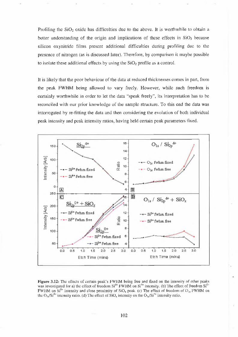
Profiling the SiC>2 ox ide has d ifficu lties due to the above. It is w orthw hile to obtain a
better understanding o f the origin and im plications o f these effects in SiC>2 because
silicon oxynitride film s present additional d ifficu lties during profiling due to the
presence o f nitrogen (as is d iscussed later). Therefore, by com parison it m aybe possib le
to iso late these additional e ffec ts by u sing the SiC>2 profile as a control.
It is lik e ly that the poor behaviour o f the data at reduced th icknesses com es in part, from
the peak FW H M being a llow ed to vary freely. H ow ever, w h ile such freedom is
certainly w orthw hile in order to let the data “speak freely”, its interpretation has to be
reconciled with our prior know ledge o f the sam ple structure. T o this end the data was
interrogated by re-fitting the data and then considering the evolu tion o f both individual
peak intensity and peak intensity ratios, having held certain peak parameters fixed .
Etch T ime (mins) Etch Time (mins)
Figure 3.12: The effects of certain peak’s FWHM being free and fixed on the intensity of other peaks was investigated for a) the effect of freedom Si0+ FWHM on Si4+ intensity, (b) The effect of freedom Si0+ FWHM on Si0+ intensity and close proximity of SiOx peak, (c) The effect of freedom of 0 ]s FWHM on the 0 | s/Si4+ intensity ratio, (d) The effect of SiOx intensity on the 0 | S/Si4+ intensity ratio.
102
In order to investigate the effect o f the substrate peak FW H M b eing free on the oxide
peak intensity during w et chem ical profiling, the S i2 P spectra o f figure 3.11 (for normal
incidence) w ere refitted w ith the substrate peak FW H M free and fixed . Figure 3 .12 (A )
sh ow s the S i4+ ox id e intensity versus etch tim e w ith the s ilico n S i0+ substrate peak
FW H M fixed (sh ow n in black) and free (sh ow n in red); both data sets lie on the same
curve. The tw o data sets are very sim ilar, suggesting the S i4+ ox id e peak FW H M is not
affected by the substrate, w h ich is reasonable g iven the distance b etw een the oxide and
substrate peaks.
In order to investigate the change ( i f any) o f the substrate S i0+ peak FW H M and the
effect o f the adjacent SiO x suboxide peak on the substrate intensity figure 3 .12 (C)
sh ow s the s ilico n S i0+ substrate intensity versus etch tim e w ith its FW H M free to vary
(sh ow n in B lue) and fixed (sh ow n in pink). In itially both in tensities are similar, but, for
longer etch tim es the substrate intensity o f the free FW H M data (B lue) grow s relative to
the intensity o f the fix ed FW H M data (show n in Pink). T he tendency o f the substrate
peak FW H M to grow for long etch tim es m ay be arise from broadening o f the substrate
peak due to interfacial hydride bonds. To see h o w the substrate intensity is affected by
the c lo se proxim ity o f the suboxide S iO x peak intensity, the substrate intensity plus the
su boxid e intensity w h en the substrate FW H M is free (red) and fixed (black) respectively
are a lso sh ow n in figure 3 .12 (c). T he d ivergence b etw een the b lue and pink for long
etches and the relatively constant agreem ent b etw een the red and b lack suggests that the
SiO x suboxide peak intensity grow s w h en the substrate F W H M is fixed , only at the loss
o f the neighbouring S i0+ substrate intensity.
In order to investigate the im pact o f p ossib le hydrocarbon contam ination and suboxide
signal contribution to the o x y g en peak intensity figure 3 .12 (B ) sh ow s the ratio o f the
O is o x y g en peak intensity to S i4+ ox id e peak intensity w ith the o x y g en FW H M free
(red) and fix ed (b lack) respectively . In the black graph the o x y g en FW H M to w as held
to its as-received value to try to lim it the p ossib le e ffec t o f any hydrocarbon
contam ination contribution to the peak at sm all ox id e th ickness. A fter all, the oxygen
peak intensity has contributions from the contam ination and suboxide layers w hich
cannot be d e-convolu te from it. T hese contributions sustain the oxygen intensity w hile
the ox ide intensity d ies. I f the o x y g en FW H M value is held to its as-received values
103
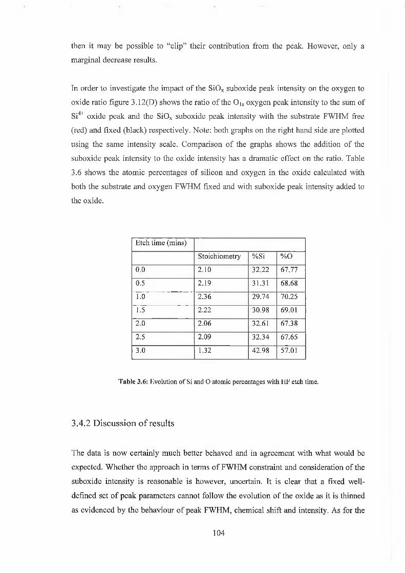
then it m ay be p ossib le to “clip ” their contribution from the peak. H ow ever, on ly a
m arginal decrease results.
In order to investigate the im pact o f the SiO x suboxide peak intensity on the oxygen to
oxide ratio figure 3 .1 2 (D ) sh ow s the ratio o f the O is o x y g en peak intensity to the sum o f
Si4+ o x id e peak and the SiO x suboxide peak intensity w ith the substrate FW H M free
(red) and fix ed (black) respectively. N ote: both graphs on the right hand side are plotted
using the sam e intensity scale. C om parison o f the graphs sh ow s the addition o f the
suboxide peak intensity to the ox id e intensity has a dramatic e ffec t on the ratio. Table
3.6 sh ow s the atom ic percentages o f silicon and o x y g en in the ox id e calculated w ith
both the substrate and oxy g en FW H M fixed and w ith su boxid e peak intensity added to
the oxide.
Etch time (mins)
Stoichiometry %Si % o
0.0 2.10 32.22 67.77
0.5 2.19 31.31 68.68
1.0 2.36 29.74 70.25
1.5 2.22 30.98 69.01
2.0 2.06 32.61 67.38
2.5 2.09 32.34 67.65
3.0 1.32 42.98 57.01
T able 3.6: Evolution o f Si and O atomic percentages with HF etch time.
3.4.2 Discussion of results
The data is n o w certainly m uch better behaved and in agreem ent w ith what w ould be
expected . W hether the approach in terms o f FW H M constraint and consideration o f the
suboxide intensity is reasonable is how ever, uncertain. It is clear that a fixed w ell-
defined set o f peak parameters cannot fo llo w the evo lu tion o f the ox id e as it is thinned
as ev id en ced b y the behaviour o f peak FW H M , chem ical sh ift and intensity. A s for the
104

intim ate relationship betw een suboxide and substrate intensity, it is reasonable to hold
the FW H M o f the substrate constant. The tendency o f the substrate peak to displace the
suboxide peak at the detrim ent o f it ’s intensity is driven by the fitting program ’s desire
for a good fit. W e proceed on the bases that w e are consisten t in our quantification
m ethod for each sam ple and so the data constraints for the SiC>2 system are applied
identically to the S iO N system . Incidentally such restraints cou ld not be applied to the
bom barded SiC>2 system because here the silicon netw ork is progressively damaged
m ore and m ore for each bombard cy c le and the FW H M is legitim ately larger (and
incalculably so) reflectin g this dam age as the S i-O -S i bond angle has been randomised
resulting in peak broadening.
3.5 HF / Ar+ bombard comparison
The above approach to quantification, form ulated after analysis and re-analysis o f
experim ental data is n o w m ore consisten t and a llow s for m ore reasonable inter sample
com parisons. In perform ing w et chem ical depth profiles o f the ox id e layers it was
p ossib le to m ake direct com parison w ith the results from the argon bombarded sam ples
in order to h igh ligh t d ifferences in suboxide signal and to lend w eigh t to our
interpretation o f the bombarded induced suboxide signal as been surface localised.
T hese d ifferences w ere further investigated by su ccessiv e ly argon bom barding a 5.5 nm
S i0 2 ox id e to realise the sam e th ickness as obtained by w et ch em ical etching. Figure
3.13 sh ow s the w e t chem ical HF and argon bom bardm ent profiles o f a SiC>2 film . An
ion current o f 0 .7 p A and an ion voltage o f 2 keV realised an etch rate o f 0 .7 nm per
m inute. The average etch rate for 0.5% HF w as 1.9 nm per m inute. In each case a fresh
sam ple w as used. T ables 3 .7 and 3.8 sum m arise the peak parameters.
105

A rgon ion B om b ard m en t
A lk a R ela tive In tensity A lk a F W H M
Thic,
(nm )
SÌ2p3/2
I4+
S l2p3/2
jOX+Sl2p3/2
I°+%
O /Si
AE0X+0+
E tch
(m in)
Si2p
Oxide
Si2p
Subx
Sl2p3/2
Subs
o ls AE
O-Si
5.8 75 — 25 2.10 — 0 1.44 — 0.83 1.60 430
4.5 64 3 33 2.0 2.1 0.5 1.97 1.7 0.95 1.72 429.6
3.0 52 6 42 1.97 1.9 1.2 2.12 1.7 0.93 1.75 429.8
2.4 40 8 52 1.9 1.8 1.6 2.25 1.7 0.96 1.78 429.5
1.5 26 8 65 1.91 1.7 2.1 2.31 1.7 1.1 1.8 429.6
Table 3.7: Evolution o f O and Si XPS peak parameters for different thickness realised by Ar+ ion bombardment.
D ilu te H f etch [0.5% ]
A lk a R ela tive in tensity A lk a F W H M
Thic.
(nm )
Sl2p3/2
I4+
SÌ2p3/2
JOX+Sl2p3/2
I ° +%
O /Si
AEox+ 0+
E tch
(m in)
SÌ2p
Oxide
Si2p
Subx
S l 2p3/2
Subs
Ols AE
O -Si
5.7 74 — 26 2.08 ------ 0 1.41 — 0.82 1.63 429.6
4.7 67 — 33 2.11 -- 2.0 1.40 — 0.82 1.67 429.5
3.4 53 — 47 2.0 -- 4.0 1.50 — 0.85 1.75 429.7
2.6 39 3 57 2.0 1.5 4.8 1.37 1.7 0.83 1.80 429.5
1.7 22 5 72 1.97 0.6 6.1 1.35 1.7 0.89 1.88 429.6
Table 3.8: Evolution o f O and Si XPS peak parameters for different thickness realised by dilute HF acidetching.
106

Chemical Etch | Ai* Bombardment ¡
Substrate
-Qi_
>±=iCOCZu
Binding Energy [eV] Binding Energy [eV]
Figure 3.13: The damaging effects of Ar+ bombardment are apparent by comparing the Si2p spectra for various thicknesses realised by both bombardment and wet chemical HF etching. For the bombarded samples (right) a larger peak FWHM is evident and an increase of suboxide signal relative to the wet chemical thickness.
The key result in figure 3 .13 is the need for a suboxide peak im m ediately after
bom bardm ent w here as in the w et ch em ically etched spectra a suboxide peak does not
em erge until a th ickness o f approxim ately 2 . 6 nm has been realised.
The S iO x peak, reflecting the qualitatively presence o f suboxides, lies closer to the
substrate peak than to the S i4+ peak. The substrate FW H M show s a gradual but small
increase as the substrate is approached. The expectation o f the intermediary peak is that
it is “fo llo w in g ” this evolu tion o f the substrate. H ow ever, w hen alm ost all ox ide is
rem oved, the peak tends to sit directly underneath the substrate peak and thus becom es
im possib le to fit w ith a high degree o f confidence. A lso , in the thickness range where
the interm ediary peak establishes itself, the ox id e peak has becom es broad, sm all,
poorly defined and also d ifficu lt to fit consistently .
107

The detection o f suboxides during w et chem ical treatment as prim arily interfacial in
origin is based on the fo llow in g observations:
W hen 2 0 nm and 13.4 nm thick ox id es w ere bom barded to a th ickness w here the
substrate cou ld be detected and fitted, the substrate FW H M value w as larger than in the
as received sam ples (5 .5 , 6 .5 , 7 .2 nm ) and continued to increase w ith bombardment.
The substrate FW H M increase w as associated w ith the reduced outer dam age region.
There w a sn ’t any need to fit an interm ediary peak in the as received thickness (5 .5 , 6.5
or 7 .2 nm w here the substrate could be fitted). Therefore, the detected suboxides signal
cannot originate from the interface.
A suboxide peak is necessary in bom barded sam ples in the ultra-thin regim e w h ile
unnecessary in w et ch em ica lly etched ox ides o f the sam e th ickness. Suboxides can be
detected in w et ch em ica lly thinned ox id es on ly at certain th ickness near the interface.
W hile the literature could attribute the ox ide FW H M increase to random bond angle
rearrangem ent, an increase in substrate FW H M , w h ich lies w e ll b e lo w the expected
dam age zon e for 2 k eV ions is m ore lik e ly to arise from surface loca lised lo w oxidation
states (i.e . S i1+ or S i2+) w h o ’s line shapes w ou ld overlap w ith the substrate.
T he above observations supported the con clu sion that suboxide sp ecies detected after
bom bardm ent w ere surface localized . The absence o f any su boxid e for oxides o f the
sam e th ick ness prepared w et chem ically a long w ith o ff-an g le behaviour supports the
dam age as b ein g surface localised .
3.5.1 Discussion o f results
W et chem ical etch ing appears to be non invasive structurally, in that surface roughing
induced by the etch ing is sm all (as show n by A F M analysis in chapter 4) com pared to
the overall film th ickness. H ow ever, the chem ical effect o f hydrogen in the acid and its
p ossib le incorporation into the ox id e or bonding at the interface in the form o f hydrides
is unknow n. T he film s under investigation are d ev ice grade d ielectric layers w hich have
108

undergone a final h igh temperature anneal in hydrogen atm osphere to reduce the
interfacial d efect density. It is p ossib le that hydrogen incorporation in the interfacial
region is responsib le for the increase in substrate FW H M as the interface is approached.
H ow ever, the use o f dilute HF for gradual thinning o f ox id e is com m on and hydrogen
induced changes have not been reported by other workers [2 2 ].
3.6 Oxynitride Analysis Overview
Incorporation o f nitrogen into ultra-thin SiC>2 film s has advantages in reducing boron
m igration from the (M O SFE T ) transistor gate, in increasing the ox id e dielectric constant
and in reducing interfacial suboxide density. H igher d ielectric constant material allow s a
thicker ox id e to be used to alleviate the transistor gate-tunnelling problem . A s nitrogen
is bonded to three silicon atom s at the interface com pared to doubly coordinated
oxygen . T his N bonding is e ffec tiv e ly m ore “com pact” than o x y g en and is more
“resistant” to form ing p ositive defects than oxygen .
A num ber o f d ifferent procedures have b een develop ed to incorporate nitrogen into SiC>2
film s either during oxidation or by post oxidation, by rapid therm al annealing RTA, the
oxid e in a nitrogen am bient. T he ch o ice o f precursor (N2 O, N O and NH3 ) and process
used, affects the nitrogen spatial distribution and it’s bonding environm ent. For
exam ple, R T A [23] results in a narrow spatial concentration o f n itrogen at the interface
w h ile nitrogen incorporation during furnace oxidation sh ow s a m ore uniform
distribution o f n itrogen through out the oxide. N itrogen incorporation using N O results
in interfacial n itrogen ex istin g m ostly on the substrate side o f the S i0 2 /S i interface and a
sm all am ount incorporated into the bulk ox id e [24]. Incorporation u sing N 2 O results in
interfacial n itrogen ex istin g m ostly on the oxide side o f the S i0 2 /S i interface and a
larger am ount incorporated uniform ly in the oxide. N itridation using NH3 results in
nitrogen rich reg ion s at both the interface and surface w ith a sm all amount incorporated
into the ox id e [25].
A ll incorporation m ethods result in a nitrogen “p ile up” at the interface. E xcess N at the
interface has the detrim ental effec t in M O SFE Ts o f reduced carrier m obility in the
channel and enhanced electron trapping’ [26-27]. L ucovsky et al [28] have sought to
109
engineer the ideal nitrogen distribution through a tw o step p lasm a process giving a
nitrogen rich surface and g iv ing a sm all n itrogen concentration in the oxide and
interface.
W hile the se lec tiv e incorporation o f nitrogen into stacked O N dielectrics using PEC VD
m ay realise the optim al nitrogen distribution. Such p rocesses have not yet been
optim ised for current sub m icron C M O S production tech nolog ies.
Figure 3 .19 sh ow s the nitrogen SIM S profiles associated w ith the traditional nitridation
p rocesses d iscussed above. N ovak [29] et al in a recent ex ten siv e rev iew concluded that
u sing grazing incidence and lo w energy beam s, SIM S can g iv e both the distribution and
concentration o f nitrogen in ultra-thin silicon oxynitrides w ith acceptable accuracy. This
inform ation is com plem entary to X P S studies w here the chem ical bonding o f the
incorporated nitrogen can be profiled u sin g either A R X P S or w et chem ical treatment.
Shallenberger et al [20] have outlined h o w X P S also offers quantitative information,
from h om ogen ou s sam ples using integrated peak areas and applying relative sensitivity
factors. H ow ever, nitrided sam ples are problem atic because the sam ples have an
inh om ogeneous distribution o f nitrogen w ith in the sam pling depth. The signal is
detected from the S iO N layer (w h ich m ay have a non-uniform N distribution) as w ell as
from the substrate and an adsorbed surface organic layer. G iven these d ifficu lties m uch
o f the quantification has been undertaken in SIM M S [29-30], M IES [31] and N R A [32]
studies w h ile X P S has concentrated on the nitrogen chem ical state.
In order to depth p rofile the nitrogen distribution, the ox id e layers w ere w et chem ically
etched u sin g dilute HF acid solutions as for S i0 2 . T he fact that the nitrogen
concentration in the sam ples under investigation is lo w (« 0 .7 -3 % ) and the
photoion isation cross-section o f the N i s is sm all m eans that the detected signal is small.
N itrogen ’s bonding environm ent is related to it ’s spatial loca tion in the film [20]. It is
b eliev ed that n itrogen at the interface w hich bonds to the silico n substrate exists in a
chem ical state sim ilar to bulk S i3N 4 w ith an interfacial s ilico n bonded to three nitrogen
atom s, and has an associated b inding energy o f 397 .8 eV .
110
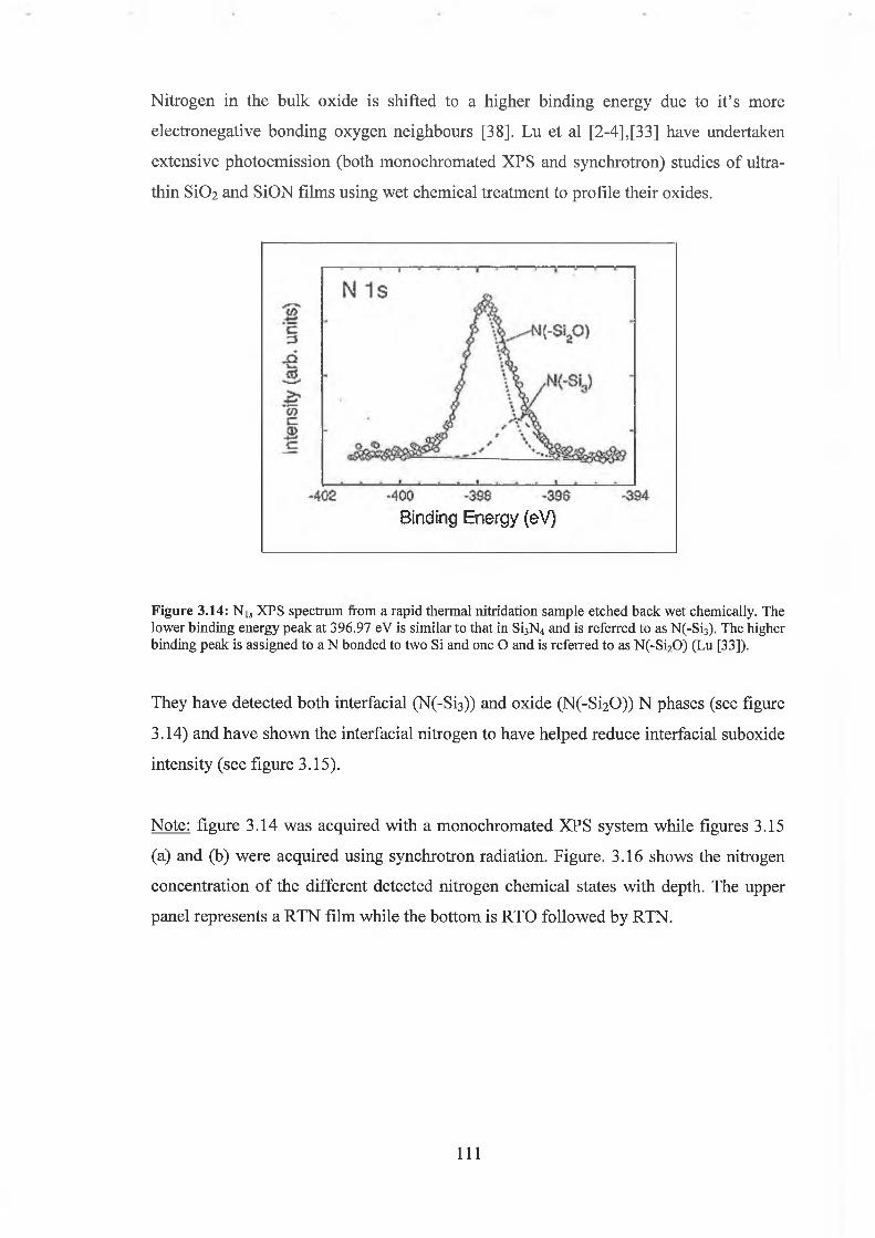
N itrogen in the bulk ox id e is sh ifted to a higher b inding energy due to it’s more
electronegative bonding oxy g en neighbours [38]. Lu et al [2 -4 ],[3 3 ] have undertaken
exten sive p h otoem ission (both m onochrom ated X P S and synchrotron) studies o f ultra-
thin S i0 2 and S iO N film s using w et chem ical treatm ent to p rofile their oxides.
Binding Energy (eV)
Figure 3.14: N ls XPS spectrum from a rapid thermal nitridation sample etched back wet chemically. The lower binding energy peak at 396.97 eV is similar to that in Si3N 4 and is referred to as N(-Si3). The higher binding peak is assigned to a N bonded to two Si and one O and is referred to as N(-Si20 ) (Lu [33]).
T hey have detected both interfacial (N (-S i3 )) and ox id e (N (-S i2 0 )) N phases (see figure
3 .14 ) and have sh ow n the interfacial n itrogen to have helped reduce interfacial suboxide
in tensity (see figure 3 .15).
N ote: figure 3 .1 4 w as acquired w ith a m onochrom ated X P S system w h ile figures 3.15
(a) and (b) w ere acquired using synchrotron radiation. Figure. 3 .16 show s the nitrogen
concentration o f the different detected nitrogen chem ical states w ith depth. The upper
panel represents a R T N film w h ile the bottom is RTO fo llo w ed b y R TN .
I l l
-10B -105 -t04 -103 -102 *101 -100 -9S -98
Binding Energy (eV)
Figure 3.15: Synchrotron photoemission Si2p spectra taken from (a) a RTO sample and (b) a RTN sample. The Si2pi/2, the background and Si4+ peak have been subtracted in order to show the reduction in suboxide state (S i1+,Si2+,Si3+) intensity due to nitrogen incorporation. (Lu[33])
L u’s b inding energy o f 396 .9 7 eV for interfacial n itrogen N (-S i 3 ) w as in excellent
agreem ent w ith that obtained for a bulk S i3N 4 film o f 3 9 7 .0 eV . H e de-convoluted the N
spectrum into an interfacial peak N (-S i3 ) and an ox id e peak ch em ica lly shifted by +0.85
eV w h ich w as attributed to N bonded to tw o s ilico n s N (-S i2 0 ) and an oxygen. H e
explains the loca lisa tion o f the nitrogen region near the interface as arising from the fact
that it’s Si atom density value (g S i3N 4 : 4 x l0 2 2 atom s/cm '3) is interm ediary betw een
that in S i0 2 (g SiC>2 : 2 .2 x l0 2 2 atom s/cm '3) and that in the s ilico n substrate (g S i : 5 x l0 2 2
atom s/cm '3). Therefore, the inclusion o f S i3N 4 near the o x id e /S i interface creates a
buffer layer w h ich reduces the Si atom ic density m ism atch induced strain at the
o x id e /S i(1 0 0 ) interface. This is reasonable and is supported by the reduction o f
interfacial su boxid e signal in the nitrided sam ples as illustrated in figure 3 .15.
112

0 to 20 30 40 50Film T h ic k n e s s (A)
Figure 3.16: N concentration profiles as a function of oxynitride film thickness for (a) a RTN sample and b) a RTO/RTN sample. The data show that the N(-Si3) is distributed mainly within the first 1 nm region o f the interface while the N(-SizO) is distributed mainly about 2 nm away from the interface (Lu [33]).
W hat appears unreasonable about L u ’s findings in th is w ork is h is assignm ent o f the
oxid e nitrogen phase to N bonded to tw o silicon atom s and an oxygen . A lso , no
evolu tion o f the N peak parameters w ith th ickness is m entioned suggesting the tw o N
chem ical states identified rem ain unchanged w ith th ickness.
It is arguable that there m ay be another interpretation o f L u ’s results in w hich there is no
nitrogen /oxygen bonding at any depth and w here N ex ists on ly in a S i3N 4 like phase.
This interpretation is based on the broader findings reported in the literature w hich
provide an alternative for the second observed N phase and it ’s behaviour w ith
thickness. Lu has not considered h is findings in the con text o f the disagreem ent about N
peak assignm ent / d e-con volu tion in oxynitrides w h ich ex ists in the literature. W hile
N O , N 2 O and N H 3 nitridation p rocesses result in N incorporation in both the oxide and
interface, yet there is considerable evidence to su ggest that the nitrogen bonds directly
w ith s ilico n atom s only. O xygen-n itrogen related bonds have been reported using other
nitridation process.
113

The chem ical sh ifts are in the range 1 .6-3 .0 eV [17],[34] and attributed to N -S iO iO
bonding. Chang et al [35] found peaks shifted by 3.8 and 6.1 eV , w h ich they assigned to
N -SiC hO and N -O 3 configurations respectively . T hese ch em ical shifts relating to N - 0
bond form ation are sign ificantly larger than those reported by Lu et al. A s w ill be
outlined b e lo w no ev id en ce o f direct n itrogen o xygen bond ing w as evident in the
studies present in th is thesis, although a variation in the N peak binding energy,
intensity and FW H M w ith th ickness w as found. In order to interpret our ow n results in
the context o f th is d isagreem ent a b rief outline it’s origins and im plications is given.
For interfacial nitrogen, there is general agreem ent about it ’s bonding environm ent
b eing that o f N (-S i 3 ) but a spread in it’s binding energy o f 0 .9 eV has been found with
con flictin g interpretations [2 3 ],[3 3 ],[3 8 ].
For oxynitrides prepared u sing N 2 O (E n i s 398 .4 eV ), N O (E Ni s 3 9 8 .2 eV ) andN F b (E n is
3 97 .9 eV ) a sin g le asym m etric N (-S i3 ) peak has been detected [20]. The binding energy
o f this interfacial peak w as found to sh ow a th ickness dependence, tending to low er
binding energies (A E = 0 .4 eV ) for thinner ox ides [36]. For ultra-thin oxides consistent
peak shifts for all ox id e elem ents can be attributed to charging o f the ox ide or to im age
charge effects arising from the c lo se proxim ity o f the conducting substrate. H ow ever,
Carr and Buhrm an [23] considered the energy separation o f the N i s and O is peaks from
the S i4+ ox id e peak w ith th ickness and they found a constant value for O is-S i4+
separation but a decreasing value for the N is-S i4+ separation. They d ism issed the
p ossib ility o f structural changes associated w ith interfacial strain (as proposed by
Grunthaner [21]) as an explanation for these differences. D irect N - 0 bonding w ould
result in a chem ical sh ift o f 2 .0 -2 .5 eV per N - 0 bond (far larger than L u’s 0.85 eV
shift). H edge et al [24] a lso found a single asym m etric interfacial N peak show ing the
sam e th ickness behaviour as Carr and Buhrm ans [23]. Their SIM S profiles show ed
nitrogen to be both in the o x id e and at the interface. So h o w can it on ly ex ist in one
phase? M iura et al [37] considered the effec t o f re-oxidation on interfacial nitrogen,
exp ecting o x y g en atom s to contribute to the nitrogen b ond ing configurations as the
interfacial reg ion is “d isp laced” out into the ox id e (during re-oxidation) by the new
interface b elow . T he interfacial n itrogen w as incorporated into the ox id e but the binding
energy shift w as the sam e as found above (A E =0.4 eV ) ruling out the possib ility o f N - 0
bonding.
114
The nitrogen d ilem m a has been addressed in an ex ten sive study by Shallenberger [20]
and N ovak and independently by N o v a k [29]. T hey prepared fiv e oxynitride sam ples
through d ifferent recipes w h ich w here exam ined under identical conditions, elim inating
differences in analysis conditions as a cause o f uncertainty. T he nitridation processes
consisted of; (a) N 2 O, (b) N O ,(c) N H 3 , (d) RTP treatm ent (I) and (e) H RP treatment (II).
Figure 3 .17 sh ow s the N is peaks obtained w ith peak b inding energies and a real N
concentration. T he on ly N - 0 related peak detected w as the peak at 4 02 .8 eV produced
by the (H R P) treatm ent and assigned (O -^ N -S i. A s for the interfacial peak, Car and
Burhm an [23] had attributed the increased N i s b inding energy w ith th ickness to N
N 2 Plasma II
No Plasma I
N = 3 . S E 14 399
N = 1.0 E 15 398.1 eV
■t() 5 41)0 3 «
frMirig En«rg.>' (®V)
N= 1.3 E 15 .5 eV
1--- 1--- 1—7 1--- r* 0 0 395
B iodiog Energy (eV)
Figure 3.17: High-resolution N is spectra from oxynitrides grown in a) N 20 , b) N 0 /0 2 mixture, c) NH3 d) N2RTP plasma treatment type I and e) N 2 remote plasma treatment type II. The peaks at 397.5-398.4 eV in a) to e) are due to N(-Si3). The peak at 399.7 eV d) and e) are due to 0-N (Si) 2 The peak at 402.8 eV e) is due to (0 -)2N-Si. The areal density o f the different nitrogen species is listed for the individual nitrogen coordinations ( Shallenberger [20]).
115

bonded to tw o silicon s and a dangling bond N (-S i ) 2 or a hydrogen related bond N -SÎ 2 H.
H ow ever, the absence o f a corresponding number o f associated defects in capacitance-
voltage (C V ) analysis seriously questions Car’s theory. B ou vet et al [38] proposed that
the increase in chem ical shift o f the nitrogen com ponent in the ox id e w ith thickness was
due to the increased effects o f second nearest neighbour o xygen s in the oxide.
Shallenberger [20] tested B o u v et’s [38] second nearest neighbouring oxygen theory by
calculating the areal density o f N in the fiv e sam ples. H e found a correlation (show n
figure 3 .1 8 ) b etw een nitrogen concentration and binding energy, w here there w as a shift
to higher b inding energy at low er nitrogen concentration (i.e. higher oxygen
concentration). T his trend in b inding energy w as attributed to the increasing
concentration o f o x y g en as the next nearest neighbour to the S iN 3 bonding environment.
O xygen concentration
ÎE 1 4 1 E I5 IF,}«
N areal density by X PS (atom s/cm 2)
Figure 3.18: Plot o f the N(-Si)3 nitrogen l s binding energy as a function o f N areal density measured by XPS. The shift to higher binding energy at lower N concentration (i.e. higher O concentration) is due to the presence o f the more electronegative next nearest neighbour oxygen atoms (Shallenberger [20]).
H ow ever, w h en Shallenberger [20] com pared the X P S N areal concentrations w ith those
calculated u sin g N R A he found poor agreem ent for som e sam ples and good agreem ent
for others. T he reason for the departure o f X P S from the N R A results for som e sam ples
w as found in their SIM S profiles as show n in figure 3.19. N early all the N is p iled up in
the interface reg ion 3 .5nm b e lo w the surface in the N 2 O # 2 sam ple. S ince on average
116

the nitrogen photoelectrons are originating from deeper in the oxide than the Si4+
photoelectrons, the nitrogen signal is d isproportionately attenuated resulting in an
underestim ate o f the true nitrogen concentration by X P S .
Figure 3.19: SIMS depth profiles showing nitrogen in-depth distribution for different nitridation process (Shallenberger [20]).
The N O /O 2 sam ple exhibited a m ore uniform n itrogen distribution w ith in the oxide
layer y ie ld in g a better agreem ent w ith the N R A result.
The N 2 O #1 oxynitride had nitrogen located near the outer surface o f the layer, w hich
resulted in an overestim ate o f the nitrogen concentration, by X P S because o f the
disproportionate attenuation o f the Si4+ photoelectrons relative to the nitrogen
photoelectrons.
117

Rignanese and Pasquarello [39] having calculated core level shifts for N in various
environments support the view that the variation in the N binding energy with thickness
is related to the increased influence of next nearest neighbour oxygens. This analysis
would suggest that nitrogen exist only in a Si3N4 environment, throughout the oxide
layer.
However, in the oxide the increased influence of oxygen atoms in the second
coordination sphere results in a nitrogen chemically shifted peak at a different binding
energy to the nitrogen in the interfacial region which is less oxygen rich. The extent of
the shift is related to the extent of the nitrogen concentration. The overlap of these two
peaks results in a an asymmetric N is envelope whose intensity and position are decided
by how much of each phase that can be “seen” which is complicated by the presence of
a nitrogen rich region both at the surface and at the interface, as the surface phase is
exaggerated and the interface phase underestimated.
3.7 SiON As received
18000 -
16000 -
14000 -
12000 -
X3L_<
10000 -
£ 8000 -in£=(1) 6000 -C
4000 -
2000 -
0 -
- 2 0 0 0
Ols SiON 5.5nm
Cis
A lk ct
SÍ2 s SÍ2 p
- u _
goo goo iooo 1100 1200
K ine t ic E n e rg y [eV ]
—i-----■---- 1—1300 1400 1500
Figure 3.20: The elemental composition o f a 5.5 nm SiON film is revealed in a survey scan. The low nitrogen concentration is apparent from its relative intensity. The Cis signal arises from surface hydrocarbon contamination.
118
The oxynitride sample set investigated consisted of two thickness 5.5 nm and 3.3 nm as
determined by elliposimetry. The samples were realised by RTA of 5.5 and 3.3 nm SiC>2
wafers in a NH3 ambient in an industrial processing environment. Figure 3.11 shows an
XPS survey scan of the 5.5 nm SiON film. As with the SiC>2 samples investigated in this
study the oxide integrity was evident from the presence of only silicon, oxygen,
nitrogen and surface carbon. Each peak was scanned using a pass energy of 20 eV, a
step size of 0.15 eV and an integration time of 0.3 sec. Lu et al [33] using a
monochromated source reported scan times of several hours just to acquire the N peak
because of its small concentration and photoionisation cross section.
Kinetic Energy [eV]
Figure 3.21: Comparison o f principal photoelectron peaks (Si2p, O is and N ls) from (Top) 5.5 nm SiON and (Bottom) 3.3 nm SiON.
In order to attain reasonable intensities in this study the N window was scanned 60
times, the silicon 20 and oxygen 10 times. Figure 3.21 shows the spectra of Si2 P, Ois and
Nis in the 5.5 nm (upper panel) and 3.3 nm (lower panel) SiON samples respectively.
As shown in his SIMS profiles in figure 3.19 and explained by Shallenberger [20], NH3
annealed SiC>2 layers are particular problematic given the presence of both a surface and
interfacial nitrogen region in the oxide.
119

It is therefore interesting to speculate as to how a quantitative interpretation of the film
composition is affected as the oxide is thinned. Also, as was apparent from the
behaviour of the stoichiometry results from etched Si0 2 films already investigated; it
was necessary to establish a consistent methodology to curve fit the data sets.
Thickness
In order to accurately calculate the thickness of the SiON films using equation 2.19,
there is a need to know the value of IMFP XsioN for the oxynitrides.
d = Ln *sio2 IcIsi 1 «
+ 1 SiO,
However, as the nitrogen concentration through the film is non-uniform, the IMFP
would vary through the film. In order to proceed many researchers have simply ignored
the nitrogen concentration and calculated the thickness using the IMFP for SiC>2 . After
all, the nitrogen concentrations involved are extremely small ( < 1 at.%) and an absolute
value of thickness is not ultimately of concern. Using equation 2.19 and the Si0 2
parameters, the calculated thickness values of 5.7 nm and 2.8 nm were obtained for the
5.5 nm and 3.3 nm samples respectively.
3.71 Wet Chemical Depth Profile for 5.5 nm oxynitride
Figure 3.22 shows the evolution of the Si2 P spectrum following successively longer (0.5
min per etch) wet chemical etches for the 5.5 nm thick SiON layer in dilute (0.5%) HF
acid. A fresh sample was used in each etch cycle which consisted of etching, rinsing in
ultra pure deionised water followed by blow drying in N and insertion into UHV within
lOmins. For 0.5% HF a reduced etch rate of was observed in the SiON samples
compared to the Si0 2 layers. Other workers have also observed a reduced etch rate for
their SiON samples [42,43], The SiON samples were etched for up to 3.5 mins in steps
of 0.5 mins. The spectra on the left in figure 3.22 were acquired at 0° degree take-off
angle and those on the right at 60° degrees off angle. The Si4+ oxide and substrate peak
FWHM were both larger than in Si0 2 . Also, there was a need to fit an additional
1 2 0
suboxide related peak even before etching and, from the angular behaviour of this peak,
it appears to be interface localised.
Figure 3.22: Evolution of Si2p spectrum of 5.5 nm SiON oxide layer with wet chemical etch for (left) normal emission and (right) 60° take-off angle.
This was deduced from the fact that the suboxide peak was significantly less
pronounced in the 60° off spectra, which are more surface sensitive than the normal
emission spectra. Table 3.9 compares the spectral parameters for a 5.5 nm SiC>2 , SiON
and 3.3 nm SiON sample. The larger FWHM of the SiON samples can be attributed to
the presence of both oxides and nitrides in the film. Also, the post oxidation NH3 anneal
has most likely led to the formation of a more distributed interface resulting in the
earlier detection of suboxides. As with the Si0 2 samples, the oxide tends to a lower
binding energy and becomes poorly defined below a thickness of 2 nm.
1 2 1

A lk a FWHM SiON 5.5 nm FWHM SiON 3.3 nm
E tch
(min)
SÌ2p
Oxide
SÌ2p3/2
Subs
Sl2p3/2
Subx
Ols AE
O -Si
Si2p
Oxide
SÌ2p3/2
Subs
SÌ2p3/2
Subx
Ols AE
O-Si
0 1.62 0.87 1.7 1.72 429.6 1.73 0.92 1.7 1.81 429.7
0.5 1.54 0.85 1.7 1.67 429.8 1.65 0.94 1.7 1.79 429.5
1.0 1.56 0.86 1.7 1.71 429.7 1.61 0.93 1.7 1.81 428.6
1.5 1.63 0.87 1.7 1.75 429.7 1.56 0 .94 1.7 1.87 430.0
2.0 1.58 0.88 1.7 1.73 429.7 1.47 0.94 1.7 1.91 430.0
2.5 1.60 0.90 1.7 1.82 430.0 1.32 0.96 1.7 1.95 429.9
3.0 1.63 0.95 1.7 1.85 430.0 — 1.02 — 2.05 —
3.5 — 0.97 — 1.82 429.9 — 1.11 — — —
A lk a FWHM Si02 5.5 nm
E tch
(min)
SÌ2p
Oxide
SÌ2p3/2
Subs
AE
O-Si
Ols AE
O-Si
0 1.42 0.82 429.6 1.67 429.6
0.5 1.38 0.82 429.6 1.67 429.6
1.0 1.37 0.82 429.6 1.76 429.6
1.5 1.49 0.86 429.7 1.8 429.7
2.0 1.51 0.87 429.7 1.88 429.7
2.5 1.35 0.86 429.7 1.89 429.7
3.0 1.23 0.88 429.6 1.96 429.6
3.5 — 0.92 — — —
Table 3.9: Summary o f XPS peak parameters for oxide and oxynitride samples after dilute 0.5% HF acid etching.
Figure 3.23 (a) and (b) shows the corresponding N ls spectra also obtained at 0° take-off
and 60° degree take-off respectively. The spectra were charge corrected using the SÌ2 P
substrate at 99.3 eV as a reference. The as-received (0 min etch) N is peak was slightly
asymmetric and could be fitted well with a FWHM of 1.8 eV at a binding energy of
398.8 eV. However, as the film was thinned, this peak broadened to 2.0 eV and shifted
to 398.3 eV and finally as the interface was approached, it’s FWHM was 1.3 eV and
binding energy 397.9 eV. Given the change of the N peak envelope with thickness and
take-off angle the spectrum was fitted with two peaks instead of just one. The first peak
was an interfacial peak corresponding to SÌ3N 4 with a fixed binding energy of 397.9 and
1 2 2
a FWHM of 1.3 eV and a second peak with a FWHM of 1.6 eV who’s binding energy
was allowed to freely vary in energy position.
SiON 5.5nm Ni«
0° take-off 60° take-offSijN4 /■ \ 5 . 2 nm
— 0(Si3N4W 7 \ f \/ / Vk..
4.0 nm A/ / \ v
3.0 nm
/ \ l , m " 7 \
1.2 nmA . .
........___________________
\ 0.3 nm............ .
A
_Q !•_<
CO£ZCD-i—iC
393 396 399 402 405 408 393 396 399 402 405 408
Figure 3.23: Evolution of N ls spectrum with wet chemical etch for (left) normal emission and (right) 60° take-off angle. The peak is de-convoluted into two components an interfacial Si3N4 like peak and an oxide related phase which is tentatively assigned 0 (S i3N4).
When the charge corrected N spectra were fitted with two peaks, with only the FWHM
fixed, the binding energies of the peaks agreed with the literature values for interfacial
and surface localised nitrogen [20],[33],[36], Figure 3.24 shows the envelope of the fit
to the N spectra, the intensities are uncorrected. Normally to cater for changes in the
intensity due to difference in sample sizes, positions or off-angle shadowing effects all
peak intensities are normalised to that of the Si oxide peak. Thus, the raw intensities
cannot be compared here but the graph does convey the consistency of the peak
positions after charge correction in both the normal and off angle spectra. The vertical
hatched lines give a visual indication of the nitrogen peak positions.
S iO N S J n m N is
Binding E nergy [eY ] Binding Energy [eV]
Figure 3.24: The binding energy shift of the centre of the N )s peak with etch time and with take-off angle gives an indication of the evolution of the interface and oxide nitrogen components which make up the peak. The hatched vertical lines guide the eye to the expected binding energy positions for the interface and bulk components.
E tch T im e T h ickness (A) % O xygen % N itrogen % Silicon (O /Si)
0 52 .4 63 .44 0.35 36.20 1.75
0.5 40. L 66.76 0.14 33.09 2.01
1.0 30.1 64.89 0.14 34.96 1.85
1.5 19.3 66.42 0.21 33.36 1.99
2.0 11.7 69.50 0 .32 30.17 2.30
2.5 6.03 63.85 0.55 35.58 1.79
3.0 3.04 61.94 0.65 37.40 1.65
Table 3.10: Variation of oxygen, silicon and nitrogen elemental concentrations with dilute 0.5% HF acid etching for 5.5 nm oxynitride.
124

Table 3.10 shows the atomic percentages of each element calculated from the peak
intensities after correction for the atomic sensitivity factor. A more commonly used
measure of the nitrogen concentration in wet chemical profiles is the ratio of nitrogen
intensity to nitrogen plus oxygen [23], [40-42], This ratio identifies the difference in
normalised nitrogen signal between samples, which have been etched to different
thickness in order to determine the amount of nitrogen contained in the etched
thickness. Thus, the ratio allows a quasi depth profile of the nitrogen distribution
throughout the film to be determined, rather than the exponentially weighted average
over the complete sampling depth.
Bersani et al [43] (figure 3.25) found a higher nitrogen concentration at the interface
using NO during oxidation compared to N2 O.
V.co
Mm-O
* Wr—
0.20
0.15
•
■ •
• sam ple #4 N O
■ ssm pte #5 N gO
r*_JZ
0.1«
•
•
0.05
—t
■fa
*
•
*
■ » %« * ■ •
9 1 * 3 4 5 6 7
r e s i d u a ! t h i c k n e s s ( n i n )
Figure 3.25: Nitrogen concentration depth profiles for NO an d N 20 processes. NO results in an increased N incorporation at the interface (Bersani [43]).
Car and Buhrman [23] (figure 3.26) found a uniform N distribution using N2 O in
furnace oxidation compared to a high interface N concentration with little oxide
incorporation using N 2 O in a RTA process.
125
0.08o
2 0.06o^ 0 .0 4oS 0.02
0 . 0 0
0.10
A
© R T A
F u rn a c e
A
0.0 15.0 30.0Distance from Si Interface (A)
£
' : 1
45.0
Figure 3.26: XPS intensity ratio as a function o f distance from the S i-S i02 interface. The RTA and furnace oxides were initially 9.3 and lOnm (Car and Buhrman [23]).
Vasquez and Grunthaner et al [44-47] have under taken extensive investigations of the
nitridation process of SiC>2 films using NH3 . From modelling of the nitridation kinetics
and XPS measurements they have concluded the following:
• A surface and interface rich nitrogen region exists in the oxide.
• For a nitridation temperature of 800 °C the peak of the interfacial nitrogen
distribution remains at the interface. For temperatures above 1000 °C it moves
away from the interface due to a reduction in the diffusion of nitrogen species
and local oxidation at the substrate.
Figure 3.27 shows the XPS results of a N chemical depth profile performed by
Grunthaner et al [44]. Grunthaner’s interfacial N distribution is displaced approximately
2 nm from the interface due to the nitridation temperature (>800 °C). He found a
correlation between the nitrogen and oxygen concentrations and Si2 P chemical shift
(Eb:Si2 P4 +-Eb: Si2 P0+), where the shift was reduced in the interfacial nitrogen region and
then increased again as the substrate was approached.
126
To explain this he proposed the existence of a non-homogeneous SiC>2 region in the
oxide in which the inter-tctrahedral Si-O-Si bond angle is reduced due to compressive
interfacial stress arising from the lattice mismatch between the silicon substrate and it’s
oxide. This strained Si0 2 region is more reactive to NH3 than the bulk oxide and it is
here, within 3 nm of the interface that the nitrogen rich region is formed. He also
observed an oxygen rich region within 1.5 nm of the interface.
Figure 3.27: (a) INis/Isl2P ,where ISi2p is the corrected intensity o f the chemically shifted Si4+ oxide peak, b) W ( I Ni, + Iqis), where INis and I0 is are the N ls and Ois peak intensities corrected for photoionisation cross sections, (c) D°ox / (DN0X + D °ox), where DN0X and D °ox are the atomic densities of nitrogen and oxygen in the oxynitride, respectively (Vasquez [44]).
He attributed this region to the formation of a nitride barrier negating further nitride
diffusion in the anneal process and leaving an oxygen rich region. Alternatively, he
suggested that the oxygen rich region arises from the reaction of by products from the
Si0 2 NH3 reaction (such as hydroxyl species) with the substrate. Figure 3.28 shows the
nitrogen profiles determined in this study by the ratio method for the 5.5 nm SiON
oxide. The results suggest that a narrow nitrogen region exists at the outer surface and a
larger broader nitrogen distribution at the interface.
127
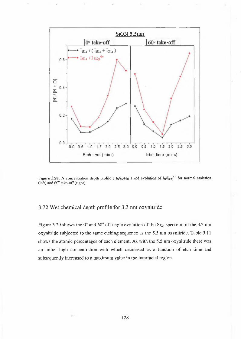
SiON 5.5nm
Etch t im e (m ins ) Etch t im e (rn ins)
Figure 3.28: N concentration depth profile ( IN/IN+I0 ) and evolution of W Isi2p4+ for normal emission (left) and 60° take-off (right).
3.72 Wet chemical depth profile for 3.3 nm oxynitride
Figure 3.29 shows the 0° and 60° off angle evolution of the Si2 P spectrum of the 3.3 nm
oxynitride subjected to the same etching sequence as the 5.5 nm oxynitride. Table 3.11
shows the atomic percentages of each element. As with the 5.5 nm oxynitride there was
an initial high concentration with which decreased as a function of etch time and
subsequently increased to a maximum value in the interfacial region.
128

Etch Time Thickness (A) % Oxygen % Nitrogen % Silicon (O/Si)
0 35.3 60.86 0.46 38.66 1.57
0.5 25.1 62.68 0.26 37.04 1.69
1.0 15.5 63.94 0.32 35.72 1.78
1.5 7.5 60.47 0.56 38.96 1.55
2 .0 4 62.73 0.83 36.42 1.72
2.5 1.7 58.60 0.79 40.59 1.44
3.0 0 99.03 0.96 0 --
Table 3.11: Variation of Oxygen, Silicon and Nitrogen elemental concentrations with dilute 0.5% HF acid etching for 3.3 nm oxynitride.
SiON 3.3 nm Si?p
0° take-off 60° take-off
A A 3 5
----------------------------------------------------------------------------------------------
- si(l+ - si4+ A
A ao 2.3nm— f c J / X —
A 1.5 nm -A A -A 0.7 nm
0.4 nm—
0.2 nm
j \ _______________“
-Q
<S'cn C QJ
96 99 102 105 108 11 1
Binding Energy [eV]96 99 102 105 108 111
Binding Energy [eV]
Figure 3.29: Evolution of Si^p spectrum of 3.3 nm SiON oxide layer with wet chemical etch for (left) normal emission and (right) 60° take-off angle.
For the 3.3 nm oxynitride a 2.5 min etch almost results in complete removal of the oxide
compared to the 5.5 nm layer. After 3 mins etching, the 3.3 nm SiON oxide peak at
normal emission was too poorly defined to fit, but in the corresponding 60° take-off
129

scan an appreciable intensity could be detected. Figure 3.30 shows the normal and 60°
off-angle behaviour of the Nis peak with thickness for the 3.3 nm oxide.
Figure 3.30: Evolution of N u spectrum with wet chemical etch for (left) normal emission and (right) 60° take-off angle. The peak is de-convoluted into two components an interfacial Si3N4 like peak and an oxide related phase which is tentatively assigned 0 (S i3N4).
Similar to the 5.5 nm SiON Nis spectra, the 3.3 nm Nis spectra were initially fitted with
a single peak to see how it’s as received value of FWHM and kinetic energy evolved.
An initial FWHM of 1.8 eV grew during the fit and finally reduced to a value of 1.3 eY.
This final value was used for the FWHM of the interfacial Si3 N4 like phase and the
FWHM for the oxide phase (1. 6 eV) was retained from the 5.5 nm fit.
130
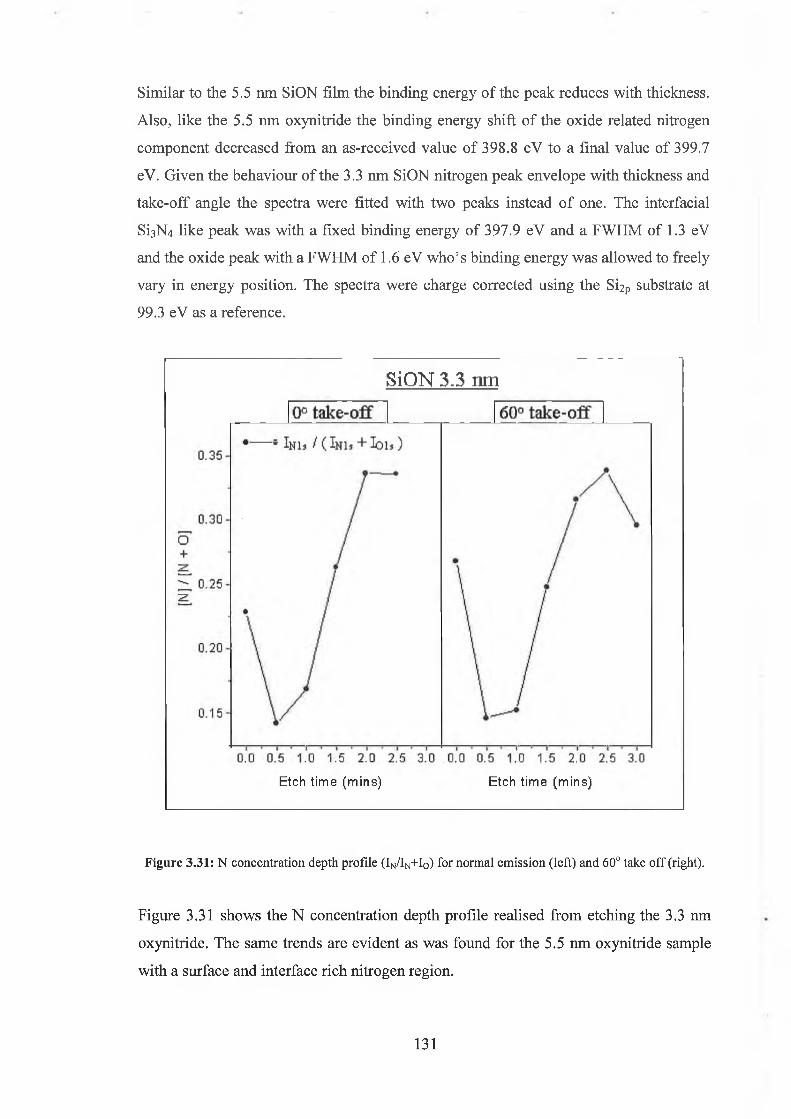
Similar to the 5.5 nm SiON film the binding energy of the peak reduces with thickness.
Also, like the 5.5 nm oxynitride the binding energy shift of the oxide related nitrogen
component decreased from an as-received value of 398.8 eV to a final value of 399.7
eV. Given the behaviour of the 3.3 nm SiON nitrogen peak envelope with thickness and
take-off angle the spectra were fitted with two peaks instead of one. The interfacial
SiaN4 like peak was with a fixed binding energy of 397.9 eV and a FWHM of 1.3 eY
and the oxide peak with a FWHM of 1. 6 eV who’s binding energy was allowed to freely
vary in energy position. The spectra were charge corrected using the Si2 P substrate at
99.3 eV as a reference.
SiON 3.3 nm
Etch t im e (m in s ) E tch t im e (m in s )
Figure 3.31: N concentration depth profile (IN/IN+I0) for normal emission (left) and 60° take off (right).
Figure 3.31 shows the N concentration depth profile realised from etching the 3.3 nm
oxynitride. The same trends are evident as was found for the 5.5 nm oxynitride sample
with a surface and interface rich nitrogen region.
131
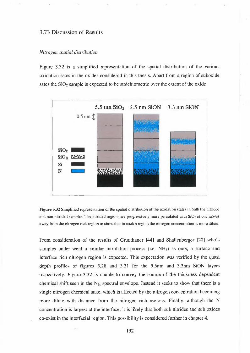
3.73 Discussion of Results
Nitrogen spatial distribution
Figure 3.32 is a simplified representation of the spatial distribution of the various
oxidation sates in the oxides considered in this thesis. Apart from a region of suboxide
sates the SiC>2 sample is expected to be stoichiometric over the extent of the oxide
5.5 nm SiC>2 5.5 nm SiON 3.3 nm SiON
F igure 3.32 Simplified representation o f the spatial distribution of the oxidation states in both the nitrided
and non-nitrided samples. The nitrided regions are progressively more percolated with S i0 2 as one moves
away from the nitrogen rich region to show that in such a region the nitrogen concentration is more dilute.
From consideration of the results of Grunthaner [44] and Shallenberger [20] who’s
samples under went a similar nitridation process (i.e. NH3 ) as ours, a surface and
interface rich nitrogen region is expected. This expectation was verified by the quasi
depth profiles of figures 3.28 and 3.31 for the 5.5nm and 3.3nm SiON layers
respectively. Figure 3.32 is unable to convey the source of the thickness dependent
chemical shift seen in the Nis spectral envelope. Instead it seeks to show that there is a
single nitrogen chemical state, which is affected by the nitrogen concentration becoming
more dilute with distance from the nitrogen rich regions. Finally, although the N
concentration is largest at the interface, it is likely that both sub nitrides and sub oxides
co-exist in the interfacial region. This possibility is considered further in chapter 4.
132

Thickness dependent chemical shift
From the behaviour of the shape and binding energy position of the Nis peak with
thickness and with take-off angle it was de-convoluted into two peaks. An interfacial
component who’s FHWM and binding energy value was chosen from the spectrum after
the longest etch (thinnest sample) where it is best seen in isolation of the oxide phase.
By holding the binding energy and FWHM of the interfacial N phase fixed the intensity
and energy position of the N oxide phase of figure 3.23 (5.5 nm SiON) and figure 3.30
(3.3 nm SiON) resulted.
The binding energy shift of the N oxide phase was found to decrease with thickness for
both samples from an initial shift of approximately 0.81 eV to a final value of
approximately 0.38 eV. These values are approximate and the change in the shift with
thickness only qualitative for the following reasons:
• For both samples a dramatic evolution of N is peak shape is evident for etch
times of 0, 0.5, 1.0 mins and with take-off angle. These etch times represent the
removal of the N rich surface region in both samples. For longer etches the
contribution of the oxide related phase is diminished as the oxide is
progressively removed. The implications of this for peak fitting are that after the
initial evolution in the N is spectral envelope it tends towards a single phase with
a resulting lack of peak structure in it’s spectral envelope making it difficult to
sustain the N oxide phase in the fitting software unassisted. In other words, it
collapses into the adjacent interfacial peak. This is essentially the same
limitation, which existed in relation to fitting interfacial sub-oxidation states in
the Si2p spectra unassisted due to the finite resolution of an XPS source.
• Also as proposed by Shallenberger [20] and discussed earlier the implications of
a surface and interface rich N region are an initial under estimation of the
interfacial phase and over estimation of the oxide related phase and due to the
attenuation and lack of attenuation of the outgoing N is signals from these
respective regions. This effect can be seen in figure 3.24 where the increase in
Nis intensity above a previous lower value from a thicker oxide thickness is
evident, over the extent of the etch profile.
133
Also the effects of shadowing, size and position for the same sample can be seen by
comparing the 0 and 60 degree of scans of the Njs intensities whereas the increase in Nis
intensity above a previous lower value which was associated with a thicker oxide
thickness is evident over the extent of the etch profile.
Stoichiometry
The interpretation of the shifted oxide related N phase has been mixed [23,24],[33]. Lu
et al [33] de-convoluted the Nis peak into an interfacial component (Si3N4 like) and
attributed a second component shifted by 0.8 eV to N -0 related bonds. However, this
shift is smaller than that expected for a N -0 related bond and there aren’t any results
from Lu about the thickness dependence of the value of the shifted component. Others
[23],[48] interpreted the large N is line width as evidence for the presence of a twofold
coordinated N atom carrying a dangling bond as in -N-Si2 or a N-Si2 H configuration.
Our results agree best with those of Bouvet et al [38] where the dispersions in the Nis
chemical shift results from N atoms in a N-Si3 configuration but with a differing number
of oxygen atoms in their next-nearest-neighbour shell. Replacing the second nearest
neighbour silicon atoms by oxygen affects the charge transfer between Si and N [39]. In
addition, there can be a variation in Eb due to core hole screening, which depends
linearly on the thickness of the dielectric layer [39],[49].
It is reasonable to expect that the variations in oxygen concentrations, which affect the
Si-N related chemical shift, should be detectable or be mirrored in a corresponding
variation in stoichiometry.
In Figure 3.12 the effects for quantification of the freedom of peak parameters (FWHM
and Ek) and the increased contributions of SiOx and hydrocarbon contamination signals
were investigated to try to recover a value of stoichiometry from the above mentioned
effects. For the same recovery prescription, the stoichiometries of the 5.5 nm and 3.3
nm SiON layers shown in Tables 3.10 and 3.11 respectively were not recovered. Unlike
the S i0 2 sample, a quantification standard for the oxynitride samples was not available.
Also, a thick oxynitride film with a surface rich nitrogen region and a thin oxynitride
film with an interfacial nitrogen rich region would allow peak parameters (IMFP, Eb and
FWHM) for both regions to be established in isolation of each other.
134
The same behaviour as found for SiC>2 might be expected with local deviations initially
and finally arising from the surface and interface N rich regions. Finally the poor
behaviour of the oxynitride stoichiometry was attributed to a convolution of the
thickness dependent effects outlined by Shallenberger et al [20] and the increased
influence of contamination and suboxide signal with reduced thickness.
3.8 Conclusion
In investigating device grade ultra-thin oxide layers using XPS, the high quality of the
oxides was affirmed by the consistency of the values of thickness, elemental
composition and stoichiometry in the as-received films. The inability to detect and
resolve the interfacial suboxide signal results from the large value of IMFP and finite
resolution of the XPS source resulting in a lack of sensitivity. In undertaking a depth
profile of the oxide, argon ion bombardment was found to be unsuitable due to the
progressive modification of the photoelectron peak FWHM and the possible
introduction of surface suboxide species making the detection of interfacial suboxide
species more difficult. The possibility of bombardment-induced suboxides would be
better-tested using synchrotron radiation and XPS measurement together. Dilute HF
acid etching was found to be uniform and consistent in removing the oxide and realising
a non-invasive depth profile. However, there are experimental quantification limitations
arising from the increased contributions of surface contamination and interfacial
suboxide species for small values of oxide thickness.
Quantification is further hindered by the inability to fit a consistent set of peak
parameters over the extent of the depth profile and the tendency of the Si2 P0+ substrate
FWHM to grow and the Si2 P4+ oxide peak to become poorly defined. Nitrogen was
detected in dilute concentrations in the oxynitride films. Dilute HF etching revealed a
surface and interface rich nitrogen region in the oxynitride films. The Nis signal was de
composed into an interfacial SisNt like signal and a chemically shifted oxide phase,
which was consistent with findings in the literature. Having applied the same peak
constrictions as were applied to SiO^ a reasonable behaviour in the oxynitride
stoichiometry was not obtained. Potentially, SIMS or NRA analysis could help here in
yielding a spatial distribution of N in the oxide. Ideally measurements at a synchrotron
135

radiation source where the N, Si and O windows could be seen at a reasonable
resolution and in which the surface sensitivity could be tuned in order to see the as-
received surface and interfacial N regions more exclusively.
136
I F. J. Grunthaner, P.J. Grunthaner, Mater. Sei. Rep. 1 (1986) 65
Z. Lu, M. Graham, J. McCaffrey, B. Brar, L. Feldman, S. Tay, Appl. Phys. Lett. 71
(1997)2764
3 Z. Lu, M. Graham, S. Tay, D. Jiang, J. Vac. Sei. Technol. B13 (1995) 1626
4 D. Mitchell, K. Clark, J. Bardwell, W. Lennard, G. Massoumi, Surf. Interface Anal.
21 (1994) 44
5 J. Shallenberger, J. Vac. Sei. Technol. A14 (1996) 693
6 R. Alfonsetti, G. Simone, L. Lozzi, S. Santucci, Surf. Interface. Anal. 22 (1994) 89
7 S. Hofmann, J. Thomass III, J. Vac. Sei. Technol. A3 (1985) 1921
8 J. W. Coburn, Thin solid films, 64 (1979) 371
9 R. Holm, S. Storp, Phys. Scr. 16 (1977) 442
1 0 G. McGuire, Surf. Sei. 76 (1978) 130
I I O Benkherourou, J P Deville, Vacuum 49 (1998) 121
1 2 E. Paparazzo, M. Fanfoni, and E. Severini, Appl. Surf. Sei. 56-58 (1992) 8 6 6
13 E. Paparazzo, M. Fanfoni, and C. Quaresima, J. Vac. Sei. Technol. A8 (1990)
2231
1 4 S. Hashimoto et al, Surf. Interface Anal., 18 (1992) 799
1 5 R. Behrisch, Sputtering by Particle Bombardment I. Springer Verlag, Berlin (1981)
1 6 R. Alfonsetti, L. Lozzi, M. Passacantando, P. Picozzi, App. Surf. Sei. 70-71 (1993)
222
1 7 M. Ebel, H. Ebel, A. Hofmann, R. Svagera, Surf. Intface Anal., 22 (1994) 51
1 8 R. Flitsch, S. Raider, J. Vac. Sei. Technol., 12 (1975) 305
1 9 M. Hecht, F. Grunthaner, P. Pianetta, L. Johansson, I. Lindau, J. Vac. Sei.
Technol., A2 (1984) 584
2 0 J. Shallenberger, S. Novak, D. Cole, J. Vac. Sei. Technol. A17 (1999) 1086
2 1 F. J. Grunthaner, P.J. Grunthaner, R. Vasquez, B. Lewis , J. Maserjian, A
3.9 References for Chapter III
137

Madhukar, Phy. Rev. Lett. 43 (1979) 1683
Z. Lu, S. Tay, T. Miller, T. Chiang, J. Appi. Phys. 77 (1995) 4110
E.C. Carr, and R.A. Buhrman Appi. Phys. Lett. 63 (1993) 54
R. I. Hegde , P. J. Tobin, K. G. Reid, Appi. Phys. Lett. 6 6 (1995) 2882
Y. Yoriume, J. Vac. Sci. Technol. B1 (1983) 67
G. Lucovsky, Y. Wu, Microelectronics Reliability 39 (1999) 365
C Mian, I Flora, Solid-State Electronics 43 (1999) 1997
G. Lucovsky, J. Non Cryst Solids 254 (1999) 26
S. Novak, Appi. Surf. Sci 175 (2001) 678
H. Hwang, W. Ting, B. Maiti, D. Kwong, J. Lee, Appi. Phys. Lett. 57 (1990) 1010
H. Lu, E. Gusev, T. Gustafsson, E. Garfunkel, M. Green, d. Brasen, L. Feldman,
Appi. Phys. Lett 69 (1996) 2713
H. Tang, W. Lennard, M. Zinke, I. Mitchell, L. Fridman, M. Green, D. Brasen,
Appi. Phys. Lett. 64 (1994) 3473
Z. Lu, S. Tay, R. Cao, P. Pianetta, Appi. Phys. Lett, 67 (1995) 2836
M. Bhat et al, Appi. Phys. Lett. 64 (1994) 1168
J. Chang et al, J. Appi. Phys. Letts. 87, (2000) 4449
R. Browning, M Sobolewski, C. Helms, Phys. Rev. B 38 (1998) 13407
Y. Miura, H, Ono, K Ando, Appi. Phys. Lett. 77 (2000) 220
D. Bouvet et al, J. Appi Phys. 79 7114 (1996) 7114
G. Rignanese, A. Pasquarello, Phys. Rev. B63 (2001) 075307
G. Tallarida, F. Cazzaniga, B. Crivelli, R. Zonca, M. Alessandri, J. Non Cryst
Solids 245 (1999)210
S. Miyazaki, T. Tamura, m. Ogasawara, H. Itokawa, H. Murakami, M. Hirose,
Appi. Surf. Sci. 159 (2000) 75
A. Kamath, D. Kwong, Y. Sun, P. Blass, S. Whaley, J. White, Appi. Phys. Lett. 70
(1997) 63

4 3 M. Bersani, L. Vanzetti, M. Sbetti, M. Anderle, Appi. Surf. Sci. 144 (1999) 301
4 4 R. Vasquez, M. Hechl, F. Grunthaner, Appi. Phys. Lett. 44 (1984) 969
4 5 R. Vasquez, A. Madhukar, F. Grunthaner, M. Naiman, Appi. Phys. Lett. 46 (1985)
361
4 6 R. Vasquez, A. Madhukar, J Appi. Phys. 60 (1986) 234
4 7 R. Vasquez, A. Madhukar, F. Grunthaner, M. Naiman, J. Appi. Phys. 60 (1986)
226
4 8 S. Kaluri, D. Hess, Appi. Phys. Lett. 69 (1996) 1053
4 9 G. Cerofolini, A. Caricato, L. Meda, N. Re, A. Sgamellotti, Phys. Rev. B61 (2000)
14157
139

Chapter 4
A chemical state investigation of the SiON and S i0 2 interface using synchrotron soft X-ray photoelectron spectroscopy
4.0 Introduction
The final oxide realised from thermal oxidation of silicon is dependent in a complex
manner on the initial surface chemical and physical state (morphology and cleanliness),
the growth conditions (substrate temperature / pressure of oxidising species) and post
oxidation treatment (high temperature anneal). Oxidation is an interfacial phenomenon,
the interface formed is distributed spatially and is comprised of structural transition
regions on both sides of the interface, which sandwich a chemical transition region.
Initially the theoretical models of the Si0 2 /Si interface in the literature are considered in
the context of their predictions and limitations and in order to form an expectation of the
interfaces examined in this thesis. The mechanism of uniform oxide removal is outlined
and surface passivation using HF acid and it’s role in the preparation of a suitable
surface for oxidation. The evolution of the interface during oxidation at various stages
of oxidation is considered in terms of initial surface morphology and the role of high
temperature post oxidation treatment. The roughness of the oxide surface during wet
chemical treatment is measured using AFM.
The results of soft X-ray (synchrotron) photoemission analysis of the Si0 2 interface are
presented and discussed. In order to realise suitable thickness (d<0.17 nm) dilute (0.5%
HF) acid etching was used to gradually profile the oxide. With the tuneable surface
sensitivity and high resolution of synchrotron radiation, the distribution and relative
intensity of sub-oxidation states in the interfacial region were resolved and measured.
From comparison with the established Si0 2 results, an attempt was made to elucidate
the interfacial Si-N bonding relationship in the Si2 P spectra of the nitrated samples.
140

4.1 Theoretical interpretation of interface
The investigation of the Si/SiC>2 interface experimentally is difficult because the
interface is buried beneath an amorphous overlayer; also its spatial extent is small and is
comprised of both chemical and structural transition regions. This is primarily because
of the inability of the oxide and substrate to form an epitaxial relationship. Most
theoretical models work by “fusing” into a slab, crystalline silicon (diamond structure)
and a crystalline form of S i0 2 (e.g. tridymite or cristobalite). In order to emulate the
amorphous nature of the oxide a randomising process of bond switching (where one of
the second neighbours of a randomly chosen atom is switched to become it’s first
neighbour, and that of the first neighbour becomes the second) and bond conversion
(where a randomly chosen Si-Si or Si-O-Si bond is swapped with a neighbour bond of
opposite type) is applied to the crystalline SiC>2 [1]. After each move, the structure is
then relaxed and the difference between initial and final energies is used to decide
whether the move is acceptable.
Theoretical models have sought to model the interface between silicon and SiC>2 in
order to examine the abruptness of the interface (i.e. is it abrupt or is it graded?) and the
distribution of the bonding states random bonding model (RBM) or random mixture
model (RMM). It is useful before considering ours and other’s experimental results to
summarises the findings of theoretical models.
Vanderbilt et al [1] in a Monte Carlo approach generated an interface, which was
contained within 2 nm of the substrate with the Si1+, Si2+ states lying closest to the^ I
substrate and the Si lying further out. This is a relatively wide interface and as
discussed later in the chapter, the experimental observation of Si protrusions as far as 3
nm into the oxide can explain the distribution of the Si3+ state and the results are in
qualitative agreement with XPS and PES studies. The model suggests a very large
density of sub-oxide states, 4.7 monolayers compared to the 1 and 2 monolayer values
found experimentally. The model doesn’t give an indication of a structural transition in
the near interfacial region as the distribution of Si-O-Si bond angles is centred at 140°,
which is the bulk oxide value. The convergence of the values on 140° is testament to the
usefulness of the approach in modelling the oxide. In other theoretical studies,
Pasquarello et al [2,3] attached tridymite (a crystalline form of Si02) to Si(100) and
141

observed a range of suboxide states for the interface formed. The model was believed to
be artificial and introduced significant stress across the interface. Subsequently using a
molecular dynamics approach they observed an abrupt interface (0.5 nm) with a
relatively small concentration of suboxides (1.5 monolayers).
Demkov et al [4] has recently pointed out the limitations of the traditional theoretical
approaches of interfacial structure modelling considered above, suggesting that some of
the results are inherent or “built into” in the construction process. For example, the
generation of a continuous random network of structures free of dangling bonds is an
inherent consequence of the Monte Carlo process used by Vanderbilt [1]. Also, the
abruptness of the interface observed by Pasquarello in his approach.
Hirose et al [5] calculated the electronic structure of the C>2 s and valence band using a
first principle molecular orbit calculation for a silicon/oxygen cluster (SiaOyllg). In
experimental valence band studies using monochromated XPS he subtracted the SiOx
and substrate valence band signal from a 0.8 nm oxide. In the resulting spectrum the
energy separation between the C>2 s and the top of the valence band was consistently
found to be 0.2 eV less than the separation in the bulk oxide. He attributed this
reduction to the extent of a shift associated with a inter tetrahedron Si-O-Si bridging
bond angle change of 140° to 130° in Si0 2 - This result is an experimental verification of
Grunthaner’s [6 ] structural transition region above the suboxide region, where
compressive stress results in the formation of smaller tetrahedral rings and the resulting
reduction in bridging bond angle gives rise to a second component in the Si4+ and Ois
peaks as described by the structure induced charge transfer model (SICT). This was a
remarkable result because of the agreement of the theoretical and experimental values
and because it affirms the existence of a structural transition region in the near
interfacial region.
There is a diversity in the results of theoretical models of the interface which likely
arises from the difficulty in modelling such a complex interface which in reality is
realised at high temperature underneath a growing oxide. However, the models
demonstrate the non-existence of an epitaxial relationship between silicon and it’s oxide
and the resulting suboxide and structural transition regions.
142
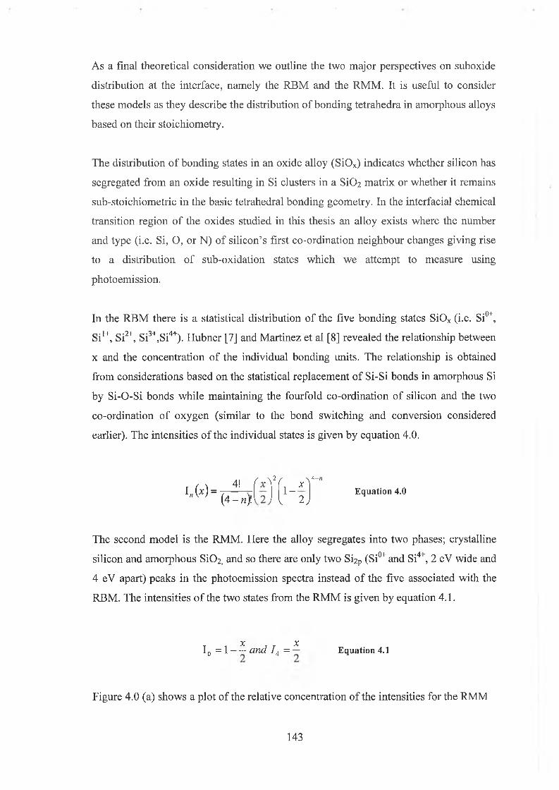
As a final theoretical consideration we outline the two major perspectives on suboxide
distribution at the interface, namely the RBM and the RMM. It is useful to consider
these models as they describe the distribution of bonding tetrahedra in amorphous alloys
based on their stoichiometry.
The distribution of bonding states in an oxide alloy (SiOx) indicates whether silicon has
segregated from an oxide resulting in Si clusters in a SiC>2 matrix or whether it remains
sub-stoichiometric in the basic tetrahedral bonding geometry. In the interfacial chemical
transition region of the oxides studied in this thesis an alloy exists where the number
and type (i.e. Si, O, or N) of silicon’s first co-ordination neighbour changes giving rise
to a distribution of sub-oxidation states which we attempt to measure using
photoemission.
In the RBM there is a statistical distribution of the five bonding states SiOx (i.e. Si0+,
Si1+, Si2+, Si3+,Si4+). Hubner [7] and Martinez et al [8 ] revealed the relationship between
x and the concentration of the individual bonding units. The relationship is obtained
from considerations based on the statistical replacement of Si-Si bonds in amorphous Si
by Si-O-Si bonds while maintaining the fourfold co-ordination of silicon and the two
co-ordination of oxygen (similar to the bond switching and conversion considered
earlier). The intensities of the individual states is given by equation 4.0.
I„W =41 i , . \ 2 i „ '\4_"
(4 - n)\1 - *
V 2 yE quation 4.0
The second model is the RMM. Here the alloy segregates into two phases; crystalline
silicon and amorphous S i02, and so there are only two Si2 P (Si0+ and Si4+, 2 eV wide and
4 eY apart) peaks in the photoemission spectra instead of the five associated with the
RBM. The intensities of the two states from the RMM is given by equation 4.1.
X XI 0 = 1 — — a n d / 4 = — Equation 4.1
Figure 4.0 (a) shows a plot of the relative concentration of the intensities for the RMM
143
(dashed lines) and the RBM (solid line). Figure 4.0 (b) shows the relative concentration
of intensities from experimental fits of SiOx layers prepared in-situ by Bell and Ley [9]
and examined by photoemission. The inability to fit core level spectra with just the two
peaks of the RMM and the good agreement between theoretical and experimental
distribution of suboxide intensities confirms the RBM distribution of oxidation states.
Figure 4.0: (a) Relative concentration of the basic bonding units (tetrahedra) shown by solid lines for the random-bonding model (RBM) and by dashed lines for the random mixture model (RMM). b) Experimental relative concentrations o f the basic bonding units vs oxygen concentration (Bell [9]).
4.2 Re-examination of Si2P chemical shift interpretation
From the above theoretical considerations the expectation of the distribution of the
oxidation states in the interfacial region is that of the RBM where there is a statistical
distribution of the five stoichiometries SiOx (X=o,i,2 ,3 ,4 )- The experimental measurement of
the relative intensities of the interfacial oxidation states is an optimal process in that
there is the need to be able to resolve the overlapping states and to exclusively
illuminate the interfacial region. In the XPS analysis presented in chapter 3, it was not
possible to resolve the individual oxidation states and after wet chemical profiling to the
144
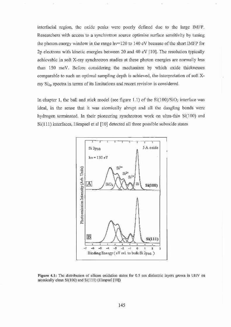
interfacial region, the oxide peaks were poorly defined due to the large IMFP.
Researchers with access to a synchrotron source optimise surface sensitivity by tuning
the photon energy window in the range hv=120 to 140 eV because of the short IMFP for
2p electrons with kinetic energies between 20 and 40 eV [10]. The resolution typically
achievable in soft X-ray synchrotron studies at these photon energies are normally less
than 150 meV. Before considering the mechanism by which oxide thicknesses
comparable to such an optimal sampling depth is achieved, the interpretation of soft X-
ray Si2 P spectra in terms of its limitations and recent revision is considered.
In chapter 1, the ball and stick model (see figure 1.1) of the Si(1 0 0 )/Si0 2 interface was
ideal, in the sense that it was atomically abrupt and all the dangling bonds were
hydrogen terminated. In their pioneering synchrotron work on ultra-thin Si(100) and
Si(l 11) interfaces, Himpsel et al [10] detected all three possible suboxide states
Binding Energy ( e V rel. to bulk Si 2p3^ )
Figure 4.1: The distribution o f silicon oxidation states for 0.5 nm dielectric layers grown in UHV on atomically clean Si(100) and Si(l 11) (Himpsel [10])
145
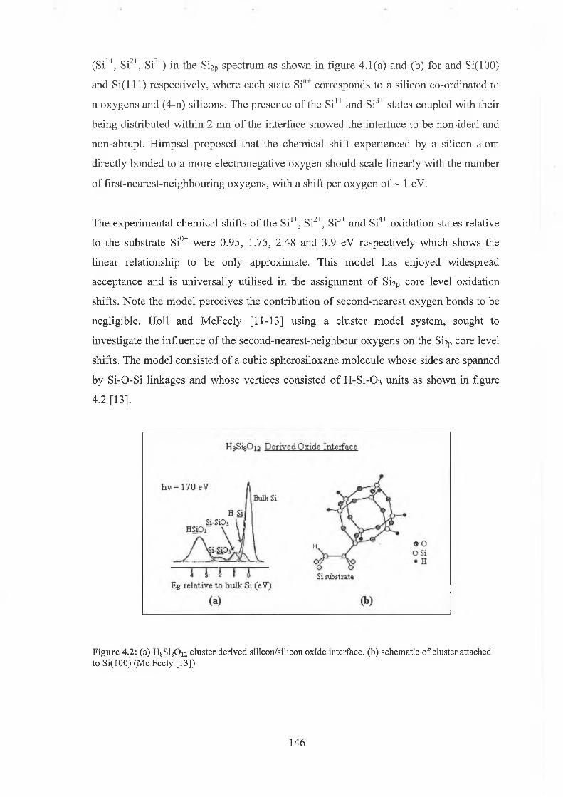
♦ 1+ -2 + ’S-!- • • *(Si , Si , Si ) in the Si2 P spectrum as shown in figure 4.1(a) and (b) for and Si(100)
and S i( l l l) respectively, where each state Si11"1" corresponds to a silicon co-ordinated to
n oxygens and (4-n) silicons. The presence of the Si1+ and Si3+ states coupled with their
being distributed within 2 nm of the interface showed the interface to be non-ideal and
non-abrupt. Himpsel proposed that the chemical shift experienced by a silicon atom
directly bonded to a more electronegative oxygen should scale linearly with the number
of first-nearest-neighbouring oxygens, with a shift per oxygen of ~ 1 eV.
The experimental chemical shifts of the Si1+, Si2+, Si3+ and Si4+ oxidation states relative
to the substrate Si0+ were 0.95, 1.75, 2.48 and 3.9 eV respectively which shows the
linear relationship to be only approximate. This model has enjoyed widespread
acceptance and is universally utilised in the assignment of Si2 P core level oxidation
shifts. Note the model perceives the contribution of second-nearest oxygen bonds to be
negligible. Holl and McFeely [11-13] using a cluster model system, sought to
investigate the influence of the second-nearest-neighbour oxygens on the Si2 P core level
shifts. The model consisted of a cubic spherosiloxane molecule whose sides are spanned
by Si-O-Si linkages and whose vertices consisted of H-Si-Ch units as shown in figure
4.2 [13].
Figure 4.2: (a) H 8Si80 i 2 cluster derived silicon/silicon oxide interface, (b) schematic o f cluster attached to Si(100) (Me Feely [13])
146
They argued that exposure of the molecule to a clean Si(100) surface would result in
attachment of the intact cube (single vertex attachment) (see figure 4.2 (b)) to one side
of a Si dimer on the (2x1) reconstructed surface along with the formation of a Si-H bond
on the other end of the dimer.
For such a structural model, the linear oxidation model predicts a single significant
Si2 P + 3 oxidation state shifted by 3.5 eV, given that the eight silicons in the cube are all
directly co-ordinated to three oxygens. Also present in the spectrum were two additional
features shifted by 1.0 and 2.2 eV. The latter was attributed to the silicon of the cube
attached to the surface. The former was attributed to the surface silicon under the
influence of the second-nearest-neighbour oxygen atom of the cube. These findings
called into question the Si2 P peak assignments of previous high-resolution oxidation
studies in the literature.
However, Raghavachari et al [14] through surface infrared measurements and quantum
cluster calculations revealed that although the single vertex attachment is
thermodynamically favoured, cube decomposition resulting in surface species via Si-0
bond scission is motivated by kinetic factors. They found excellent agreement between
XPS data and core level calculations of the chemical shifts associated with these surface
species. Pasquarello et al [15] contributed to the defence of the linear oxidation model
by showing through ab-into slab calculations that second-nearest-neighbour effects on
the core level spectrum of silicon are negligible. From the above discussion of peak
assignment the interpretation of Si2 P core level shifts adopted in this thesis are based on
the linear oxidation model with a shift of 0.9 eV per oxidation state.
4.3 Wet chemical processing
Here briefly, the mechanism by which hydrofluoric acid removes the oxide to uncover
the underlying substrate and the role it plays as a surface passivator is considered.
Himpsel’s [10] oxides were grown on atomically clean, reconstructed silicon surfaces in
UHV. At atmospheric pressure a clean Si surface quickly forms a native oxide due to
the chemically reactive un-terminated dangling bonds. The high quality oxides of
modern sub micron fabrication processes (which operate in clean environments at
147
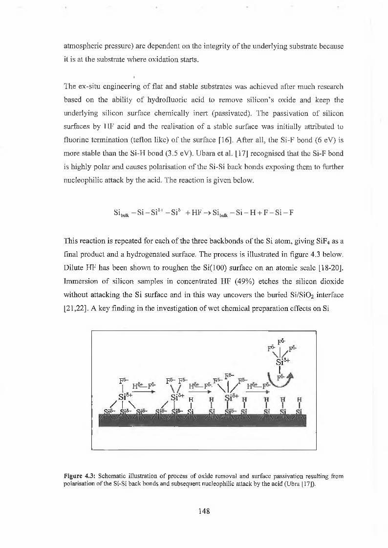
atmospheric pressure) are dependent on the integrity of the underlying substrate because
it is at the substrate where oxidation starts.
IThe ex-situ engineering of flat and stable substrates was achieved after much research
based on the ability of hydrofluoric acid to remove silicon’s oxide and keep the
underlying silicon surface chemically inert (passivated). The passivation of silicon
surfaces by HF acid and the realisation of a stable surface was initially attributed to
fluorine termination (teflon like) of the surface [16]. After all, the Si-F bond ( 6 eV) is
more stable than the Si-H bond (3.5 eV). Ubara et al. [17] recognised that the Si-F bond
is highly polar and causes polarisation of the Si-Si back bonds exposing them to further
nucleophilic attack by the acid. The reaction is given below.
Sibulk - Si - Si8+ - Si5“ + HF -> Sibulk - S i - H + F - S i - F
This reaction is repeated for each of the three backbonds of the Si atom, giving SiF4 as a
final product and a hydrogenated surface. The process is illustrated in figure 4.3 below.
Dilute HF has been shown to roughen the Si(100) surface on an atomic scale [18-20].
Immersion of silicon samples in concentrated HF (49%) etches the silicon dioxide
without attacking the Si surface and in this way uncovers the buried Si/SiC>2 interface
[21,22]. A key finding in the investigation of wet chemical preparation effects on Si
F5-
Si*+/ I \
CJ5- Oift-. C46-
J?5— J?5- F5-u— mi/— y 5— . "qH — F^- \ | / H —
. F6"
S i^I
S i * H/ I I
RfS- Si
F igure 4.3: Schematic illustration o f process of oxide removal and surface passivation resulting from polarisation o f the Si-Si back bonds and subsequent nucleophilic attack by the acid (Ubra [17]).
148

surface morphology prior to oxidation, was based on the modification of the etch pH
and the addition of impurities [23,24], Much smoother surfaces could be realised
through such modifications. For example an atomically flat hydrogen terminated silicon
H -S i(lll) surface could be realised after immersion in a buffered ammonium fluoride
HF solution with a pH of 7.8. Hagishi and Chabel [23] in an STM and infrared
absorption study obtained large (100 nm wide) unreconstructed S i( l l l) terraces with
ideal monohydride termination and separated by atomically sharp steps as shown in
figure 4.4. Hattori [24] exploited the polarisation dependent interaction of the electric
field wave vector of infrared light in selectively exciting H bond vibrational modes in
the surface region.
Figure 4.4: STM images o f Si(100) after an etch in (a) concentrated HF, (inset) FTIR spectrum showing the presence o f mono,di and tri hydrides, (b) Buffered ammonium fluoride HF solution, (inset) FTIR spectrum showing the presence o f monohydrides only which is characteristic o f a smooth surface (Chabel [23]).
Basically the absorption of p-polarised (E vector parallel to the plane of incidence)
infrared light and lack of absorption of s-polarisation (E vector normal to the plane of
incidence) infrared light indicates that the electric dipole of the Si-H bond has only a
component normal to the S i( l l l) surface characteristic of monohydride coverage, see
figure 4.5 (a). Where as on the surface etched in concentrated HF, mono, di and tri
hydrides were detected (as found by Chabel et al [23], see figure 4.4 (a) inset). Wet
chemical optimisation of the Si(100) surface cannot achieve an atomically flat surface
as indicated by the presence of mono, di and tri hydrides in both polarisations in figure
4.5 (b).149
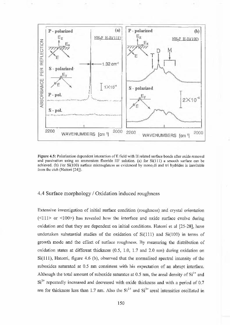
Figure 4.5: Polarisation dependent interaction o f E field with H related surface bonds after oxide removal and passivation using an ammonium fluoride HF solution, (a) for S i ( l l l ) a smooth surface can be achieved, (b) For Si(100) surface microughness as evidenced by mono,di and tri hydrides is inevitable from the etch (Hattori [24]).
4.4 Surface morphology / Oxidation induced roughness
Extensive investigation of initial surface condition (roughness) and crystal orientation
(<1 1 1 > or < 1 0 0 >) has revealed how the interface and oxide surface evolve during
oxidation and that they are dependent on initial conditions. Hatorri et al [25-28], have
undertaken substantial studies of the oxidation of S i( l l l) and Si(100) in terms of
growth mode and the effect of surface roughness. By measuring the distribution of
oxidation states at different thickness (0.5, 1.0, 1.7 and 2.0 nm) during oxidation on
S i(lll) , Hatorri, figure 4.6 (b), observed that the normalised spectral intensity of the
suboxides saturated at 0.5 nm consistent with his expectation of an abrupt interface.
Although the total amount of suboxide saturates at 0.5 nm, the areal density of Si1+ and•3+Si repeatedly increased and decreased with oxide thickness and with a period of 0.7
nm for thickness less than 1.7 nm. Also the Si1+ and Si3+ areal intensities oscillated in
150
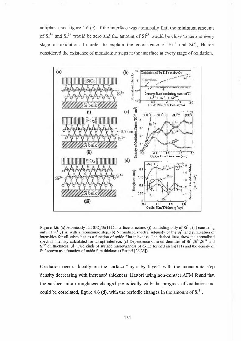
antiphase, see figure 4.6 (c). If the interface was atomically flat, the minimum amounts
of Si1+ and Si3+ would be zero and the amount of Si2+ would be close to zero at every
stage of oxidation. In order to explain the coexistence of Si1+ and Si3+, Hattori
considered the existence of monatomic steps at the interface at every stage of oxidation.
Oxidation o f Si( 111) indry02
Calculated~si*+
y4 f'Intermediate oxidation states o f Si
( Si1 + + Si2 + + Si3+ )O A 1j0 1.5
Oxide FilmTHdtness (iur£|
800 c p are
0.6 1.0 1.5 2.0Oxide FilmTlnckiiess (urn)
n -S iT lll)
1.0 i.S 2,0 Oxide Film Thickness (nir )
Figure 4.6: (a) Atomically flat S i0 2/S i(l 11) interface structure: (i) consisting only o f Si3+; (ii) consisting only o f Si1+; (iii) with a monatomic step, (b) Normalised spectral intensity o f the Si4+ and summation of intensities for all suboxides as a function o f oxide film thickness. The dashed lines show the normalised spectral intensity calculated for abrupt interface, (c) Dependence o f areal densities o f Si1+,Si2+,Si3+ and Si4+ on thickness, (d) Two kinds o f surface microughness o f oxide formed on S i ( l l l ) and the density of Si1+ shown as a function o f oxide film thickness (Hattori [26,25]).
Oxidation occurs locally on the surface “layer by layer” with the monatomic step
density decreasing with increased thickness. Hattori using non-contact AFM found that
the surface micro-roughness changed periodically with the progress of oxidation and
could be correlated, figure 4.6 (d), with the periodic changes in the amount of Si1+.
151

He explained this result in terms of the oxidation mechanism. In forming the Si1+ state
(by the insertion of an oxygen atom between two Si atoms consisting of a Si-Si bond
orientated along the < 1 1 1 > direction) the interface expands the oxide network only
along the <111> direction, while in the case of Si3+ formation the insertion of an oxygen
atom between two Si atoms consisting of a Si-Si bond at the interface expands the oxide
network mostly along the direction perpendicular to <111>. The formation of Si1+ at the
interface results in an increase in surface micro-roughness caused by the formation of
protrusions on the oxide surface.
soox: /ocrc ®oo''ci soo-c «* >--<----
Si3+ atom Si1+ atom 0.04
! e = 30
! \ s i 1++ si2++ si3+)
0 1.0 1.5 a .0 2,5 3.0 3,5 O xide Film T h ickness (nm)
Q : Silicon 11001 + : Oxygen
Si2+ Interface
1
[100]
Figure 4.7: Atomically flat S i0 2/Si(100) interface structure consisting o f (a) Si2+ only and (b) with a monatomic step, (c) (Top) Thickness dependence o f normalised spectral intensity o f Si4+ and suboxides normalised by the Si0+ intensity. The dashed line is calculated for an abrupt compositional transition. (Bottom) thickness dependence o f areal densities o f Si1+, Si2+ and Si3+. (d) changes in rms surface roughness with respect progression o f oxidation (Hattori [28]).
152
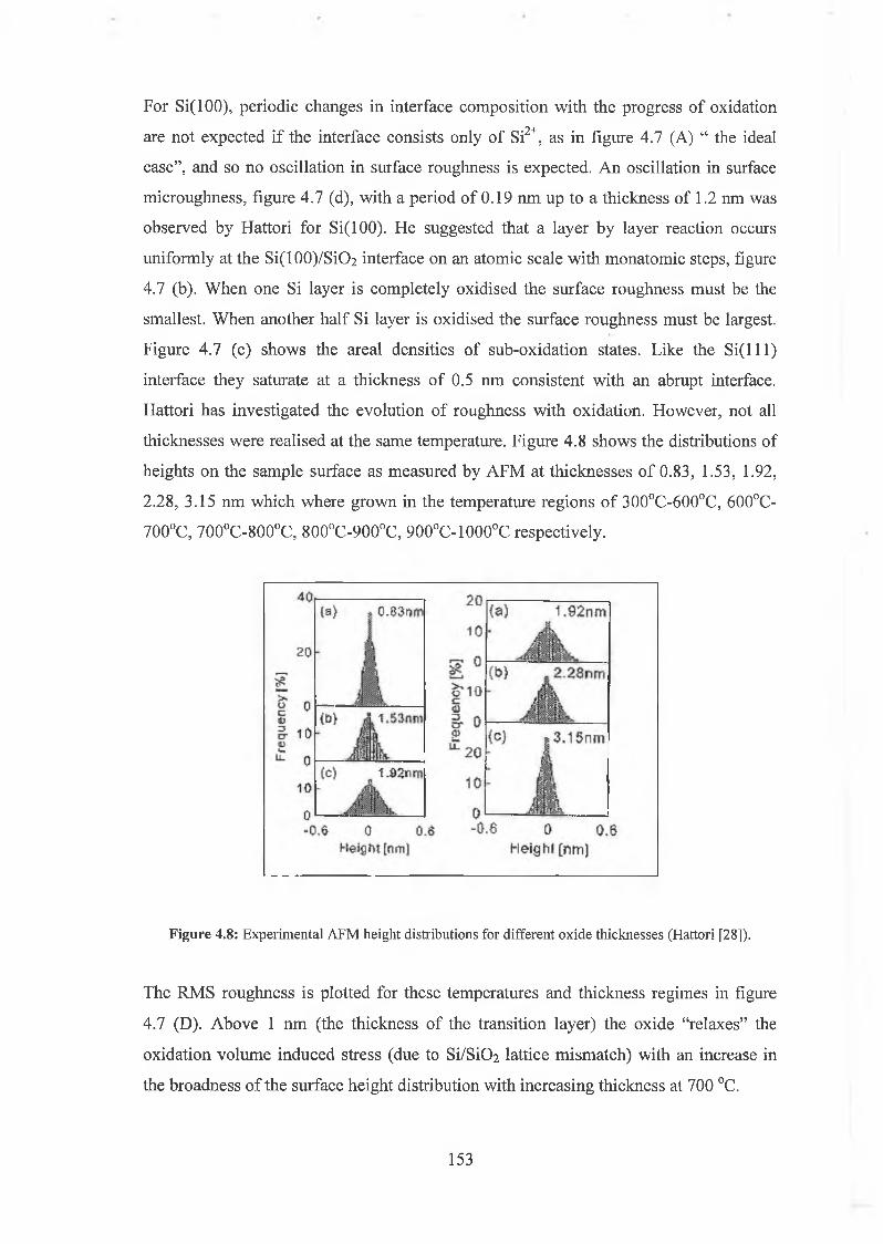
For Si(100), periodic changes in interface composition with the progress of oxidation
are not expected if the interface consists only of Si2+, as in figure 4.7 (A) “ the ideal
case”, and so no oscillation in surface roughness is expected. An oscillation in surface
microughness, figure 4.7 (d), with a period of 0.19 nm up to a thickness of 1.2 nm was
observed by Hattori for Si(100). He suggested that a layer by layer reaction occurs
uniformly at the Si(1 0 0 )/Si0 2 interface on an atomic scale with monatomic steps, figure
4.7 (b). When one Si layer is completely oxidised the surface roughness must be the
smallest. When another half Si layer is oxidised the surface roughness must be largest.
Figure 4.7 (c) shows the areal densities of sub-oxidation states. Like the S i( lll)
interface they saturate at a thickness of 0.5 nm consistent with an abrupt interface.
Hattori has investigated the evolution of roughness with oxidation. However, not all
thicknesses were realised at the same temperature. Figure 4.8 shows the distributions of
heights on the sample surface as measured by AFM at thicknesses of 0.83, 1.53, 1.92,
2.28, 3.15 nm which where grown in the temperature regions of 300°C-600°C, 600°C-
700°C, 700°C-800°C, 800°C-900°C, 900°C-1000°C respectively.
F igure 4.8: Experimental AFM height distributions for different oxide thicknesses (Hattori [28]).
The RMS roughness is plotted for these temperatures and thickness regimes in figure
4.7 (D). Above 1 nm (the thickness of the transition layer) the oxide “relaxes” the
oxidation volume induced stress (due to Si/SiCh lattice mismatch) with an increase in
the broadness of the surface height distribution with increasing thickness at 700 °C.
153
The FWHM of the height distribution decreases and saturates at 800° C. After
subsequent oxidation at 900 °C the FWHM further decreases until the roughness is on
the order of the single atomic-step height on the Si(100).
The surface roughness was found to oscillate with constant amplitude and with a period
of 0.19 nm up to a thickness of 3.15 nm, which is produced by the layer-by-layer
oxidation reaction at the interface (which occurs on an area of 5 nm2) at 700 °C and
increases with temperature.
An attempt to wet chemically profile through an oxide gives rise to a number of
questions based on the above considerations, which are. Will the etching process
roughen the surface? Using concentrated HF can the original oxide morphology be
uncovered? Will the original surface morphology be that of the final surface? The
possibility of etch induced roughness is of concern because in soft X-ray photoemission
analysis the outer atomic layers are probed due to the short IMFP of low kinetic energy
electrons. Surface roughness will lead to an increase in peak FWHM and severe
roughening would undermined thickness calculations due to local variations in oxide
thickness. Whether or not the growing oxide conserves the original interface
morphology or as predicted by the Sune et al [29] model it finishes with a flat surface
irrespective of the initial surface roughness resulting in local oxide thickness variations,
see figure 4.9(c), has huge implications for final device operation given the (exponential
dependence) sensitivity of tunnelling current to thickness variations. This issue has been
resolved to some extent by the results of Hattori above. Also, the observation of
modulations in the Fowler Nordheim tunnelling current through oxides which were
grown on purposefully roughened Si surfaces prior to oxidation by Irene et al [30]
showed no dependence of oscillation amplitude on roughness. According to the Sune
model the distribution of oxide thickness would “de-phase” tunnelling electrons and
thus rougher samples should exhibit a larger dampening in the tunnelling current
oscillation amplitude.
Before considering our oxide roughness results in the context of the above, it is useful to
examine the effect of temperature on roughness given that the oxides studied in this
thesis were grown at high temperature and have undergone a high temperature post
oxidation anneal. Hattori [28] above, figure 4.7(d), observed a decrease in surface
154

microughness for oxidation at high temperatures. Carim and Sinclair [31] proposed an
explanation from their observation of roughness behaviour with oxidation temperature
using transmission electron microscopy (TEM). Figure 4.9(a) shows a high-resolution
micrograph of the interface in which the silicon protrusions from the substrate are
clearly visible. Carim suggests the degree of interface roughness is decided by two
competing processes. Those which contribute to interfacial aspirates (initial surface
irregularities, local fluctuation in interface reaction rate) and those which alleviate
roughness (the transition to diffusion limited growth during oxidation, stress relaxation
at high temperatures or long times by viscous flow and de-localisation of strain during
growth). During oxidation, expansion occurs and creates stress, see figure 4.9(b) in the
oxide with lateral compressive strain in the oxide and tensile strain in the near interface
silicon. From consideration of the increase in free volume associated with protrusions,
Carim suggested that the interface oxidation reaction rate was accelerated in flat regions
between protrusions making the protrusions more pronounced as oxidation progressed.
Figure 4.9: (a) High-resolution transmission electron micrograph indicating non-uniform oxidation resulting in roughness o f the substrate/oxide interface, (b) Changes in the substrate and oxide strains resulting from differences in accessible volume at protrusions, (c) Growth models for the oxide, (d) Reduction o f interfacial protrusions during continued oxidation requires accelerated oxidation at the asperities with respect to the flat surface (Carim [31]).
155

The interface reaction rate variations lose their significance as the supply of oxygen to
the interface becomes rate diffusion limited leading to a greater oxidation rate under the
thinner oxide at protrusions, figure 4.9(d). The final consideration in the interplay
between roughening and smoothing is the relaxation of stress at high temperatures with
the onset of the viscose flow region in the oxide where the reduction of planar interface
stress and localised stress concentrations assist in the redistribution of silicon atoms
away from protrusions by interfacial diffusion. Thus, ultimately the effect of a long
anneal at high temperature is to reduce interface roughness.
4.5 Atomic Force Microscopy Analysis
The following is an account of our AFM analysis of oxide morphology and it’s
evolution during wet chemical etching. An AFM image is rendered through the electro
mechanical interaction of a sharp (radius of curvature of tip ~ 30 nm) vibrating (at a
resonance frequency) SiN tip with the topography of the underlying surface. By
optimising the feedback loop gains (which seek to maintain a constant tip sample
interaction) and imparting a relatively small amount of energy into the surface (i.e. by
“lightly” tapping) we can gauge the surface roughness through the root mean square
(RMS) roughness value. The surface roughness of the SiC>2 and SiON samples were
measured both as received and after each etch. All measurements were performed in
tapping mode as opposed to contact mode to avail of better sensitivity and reduced
interaction with surface contamination. Figure 4.10 shows a screen shot of the software
window as seen on the machine during analysis. Here a lpxn x lpni area of an as
received 5.5 nm SiC> 2 sample was examined in both height (LHS) and amplitude (RHS)
mode. The “granular nature“ nature of the oxide is visible in the images.
156
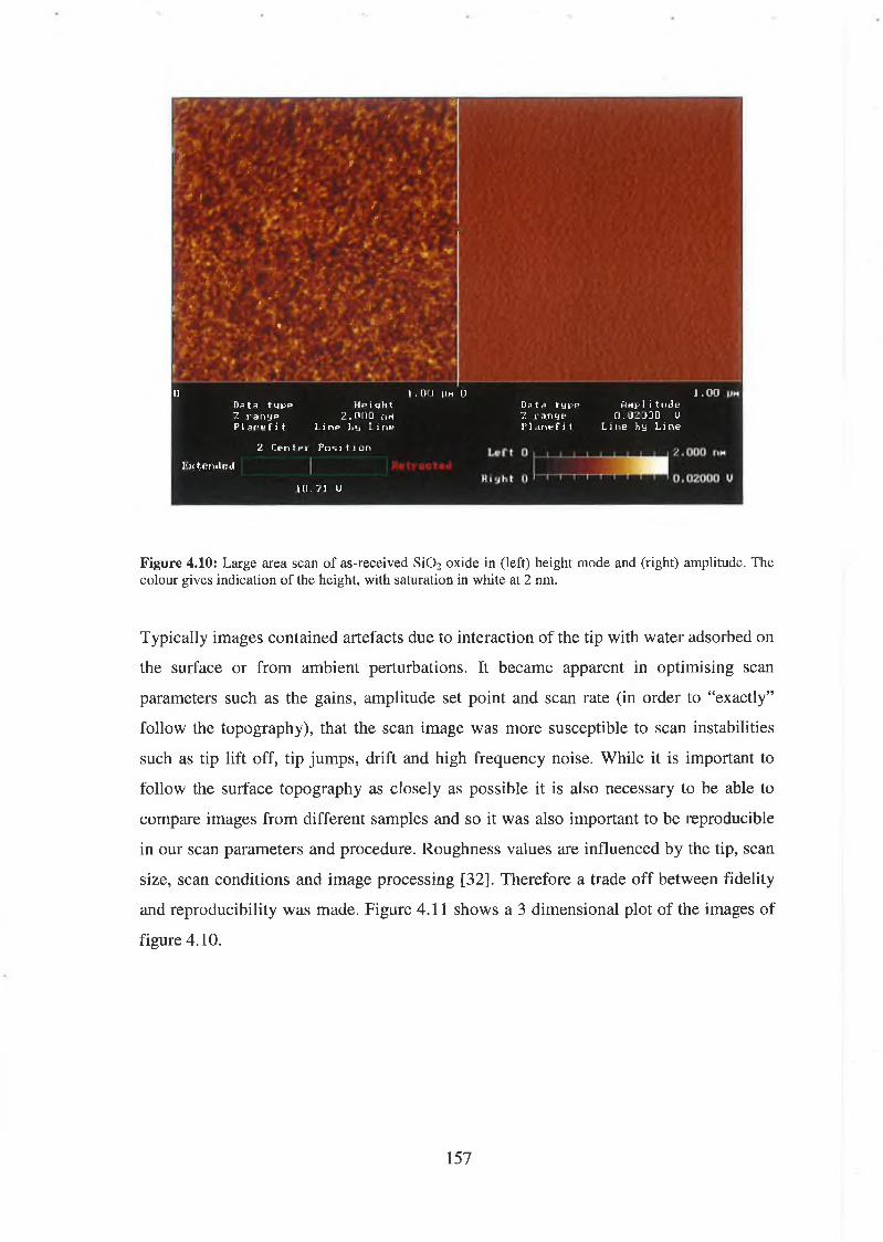
1 . 0 0Data type Amplitude2 range 0.020'DQ UPlanefit Line by Line
2 Center Position
I'xtQridtia10.71 U
Figure 4.10: Large area scan of as-received S i0 2 oxide in (left) height mode and (right) amplitude. The colour gives indication of the height, with saturation in white at 2 nm.
Typically images contained artefacts due to interaction of the tip with water adsorbed on
the surface or from ambient perturbations. It became apparent in optimising scan
parameters such as the gains, amplitude set point and scan rate (in order to “exactly”
follow the topography), that the scan image was more susceptible to scan instabilities
such as tip lift off, tip jumps, drift and high frequency noise. While it is important to
follow the surface topography as closely as possible it is also necessary to be able to
compare images from different samples and so it was also important to be reproducible
in our scan parameters and procedure. Roughness values are influenced by the tip, scan
size, scan conditions and image processing [32]. Therefore a trade off between fidelity
and reproducibility was made. Figure 4.11 shows a 3 dimensional plot of the images of
figure 4.10.
„ , , ' * .v -
Yf ' =* • • *7 w I 'I . ■: ■ ' ■ .
/ tV .. / ■ V "■ ^ , / < / ; f '
I
« *■ « ' # » i . . r*W K nim 'f ^ ' 5/ ^ ' V J, ^ r . %t '' * »*
i • * .i- . - 1 4 ', j » . .
L■;
0 i . 0-0 [IH UData type HeightZ range 2.000 runPlanefit Line by Line
157

Figure 4.11: 3 dimensional plot of the surface topography in (left) height and (right) amplitude mode.
S e c t i o n A n a l y s i s
C u rso r: fi><*d 3 Zoo«: 2 :1 c#n iin*: orr orr«t.: orr
LRMSIcR a C lc iRnaxRzRz Cnt
I R a d iu s I Si 9 Ha
966.80 oh 0.204 nH DC0 .1 6 2 nn 1 .0 9 9 rtM 0 .8 35 nn v a l i d 16 .4 6 5 uh 2 . 1 1 ? nn
S u r fa c e d i s t a n c e H o riz d is t a n c e iJert d is t a n c e flnsr I eS u r fa c e d is t a n c e H o riz d is t a n c e U e rt d is t a n c e f in a le
2 3 7 .4 6 oh 2 8 7 .1 1 nH 0 .90 3 nn 0 .1 8 1 deg 968.48 nn 966.8 0 nn1.0 4 6 nM 0 .0 62 deg DC0 Hz0.00001 nnj
o ■ ,
T O 0 .2 5 0 .5 0 0 .7 5MH
1 .2 5
c l 0 255*.0 0 6
S p e c tru H
Figure 4.12: The uniformity of surface topography across the sample is considered by considering the agreement between roughness sampled along the coloured lines shown. The spectrum gives information of possible periodicity in surface features.
In figure 4.12, cross-sections of the image show the topography in the directions of the
red, green and white lines. The uniformity of the sample topography across the extent of
the sample is affirmed by the agreement in each section. The frequency spectrum of the
158
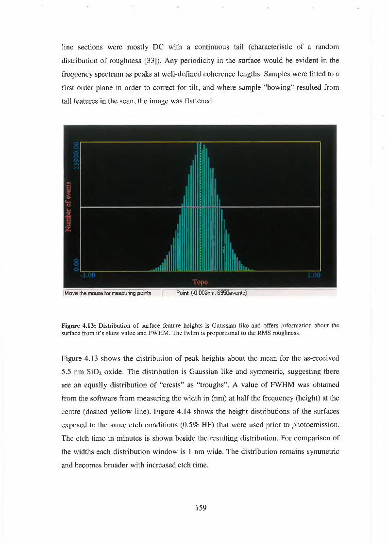
line sections were mostly DC with a continuous tail (characteristic of a random
distribution of roughness [33]). Any periodicity in the surface would be evident in the
frequency spectrum as peaks at well-defined coherence lengths. Samples were fitted to a
first order plane in order to correct for tilt, and where sample “bowing” resulted from
tall features in the scan, the image was flattened.
|Move the mouse for measuring points Point: (-0.002nm, G950events)
Figure 4.13: Distribution of surface feature heights is Gaussian like and offers information about the surface from it’s skew value and FWHM. The fwhm is proportional to the RMS roughness.
Figure 4.13 shows the distribution of peak heights about the mean for the as-received
5.5 nm Si0 2 oxide. The distribution is Gaussian like and symmetric, suggesting there
are an equally distribution of “crests” as “troughs”. A value of FWHM was obtained
from the software from measuring the width in (nm) at half the frequency (height) at the
centre (dashed yellow line). Figure 4.14 shows the height distributions of the surfaces
exposed to the same etch conditions (0.5% HF) that were used prior to photoemission.
The etch time in minutes is shown beside the resulting distribution. For comparison of
the widths each distribution window is 1 nm wide. The distribution remains symmetric
and becomes broader with increased etch time.
159
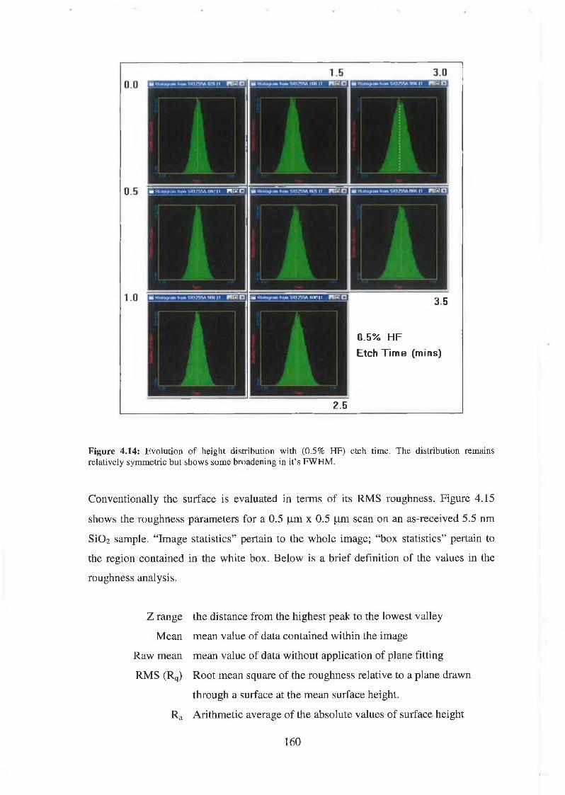
ft WH II 3.5
0.5% HF Etch Time (mins)
2.5
Figure 4.14: Evolution of height distribution with (0.5% HF) etch time. The distribution remains relatively symmetric but shows some broadening in it’s FWHM.
Conventionally the surface is evaluated in terms of its RMS roughness. Figure 4.15
shows the roughness parameters for a 0.5 |im x 0.5 |im scan on an as-received 5.5 nm
Si0 2 sample. “Image statistics” pertain to the whole image; “box statistics” pertain to
the region contained in the white box. Below is a brief definition of the values in the
roughness analysis.
Z range the distance from the highest peak to the lowest valley
Mean mean value of data contained within the image
Raw mean mean value of data without application of plane fitting
RMS (Rq) Root mean square of the roughness relative to a plane drawn
through a surface at the mean surface height.
Ra Arithmetic average of the absolute values of surface height
160
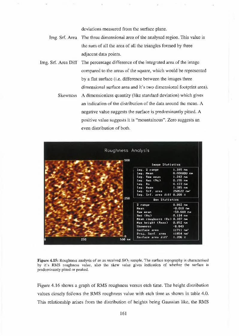
deviations measured from the surface plane.
Img. Srf. Area The three dimensional area of the analysed region. This value is
the sum of all the area of all the triangles formed by three
adjacent data points.
Img. Srf. Area Diff The percentage difference of the integrated area of the image
compared to the areas of the square, which would be represented
by a flat surface (i.e. difference between the images three
dimensional surface area and it’s two dimensional footprint area).
Skewness A dimensionless quantity (like standard deviation) which gives
an indication of the distribution of the data around the mean. A
negative value suggests the surface is predominantly pitted. A
positive value suggests it is “mountainous”. Zero suggests an
even distribution of both.
Roughness Analysis
» V * si f - * _ £ . * - ' 4 *
* ■ - » ’ A0 ” • • C*
m l? ' * ' y : - ' U
Vt - > - > » > « # ' ‘ . - V
' ■ • v a - * - ' • A ^ — Mo1 2 5 0 5 0 0 n M
I S t a t i s t i c s
j I M y . Z r a n g e 1 . 3 8 S n M
1 I M 3 . M e a n 0 . 0 0 0 0 0 0 n M
I M g . R a « M e a n 1 . 2 4 2 n M
1 M y . R m s i R q J 0 . 1 5 5 n M
! H 9 . R a 0 . 1 2 3 n M
I M g . R m s m 1 . 3 8 5 n M
1 H U . S r f . a r e a 2 5 0 S 2 2 n n *
I k * . S r l \ a r e a d i f f 0 . 2 0 9 ■/.
B o x S t a t i s t i c s
2 r a n s e 0 . 8 6 2 n M
M e a n - 0 . 0 1 8 r» M
H a w M e a n - 5 9 . 6 9 9 n M
H h s i R q J 0 . 1 3 4 n M
M e a n r o u g h n e s s i R a ) 0 . 1 0 7 n M
M a M h e i g h t ( R m a m ) 0 . 8 5 2 h m
S k e w n e s s - 0 . 0 4 3
S u r f a c e a r e a 1 1 7 1 1 n M *
P r o J . S u r f , a r e a 1 1 8 5 4 n w '
S u r f a c e a r e a d i f f 1 . 2 0 6 ’A
F igure 4.15: Roughness analysis o f an as received S i0 2 sample. The surface topography is characterised by it’s RMS roughness value, also the skew value gives indication of whether the surface is predominately pitted or peaked.
Figure 4.16 shows a graph of RMS roughness versus etch time. The height distribution
values closely follows the RMS roughness value with etch time as shown in table 4.0.
This relationship arises from the distribution of heights being Gaussian like, the RMS
161
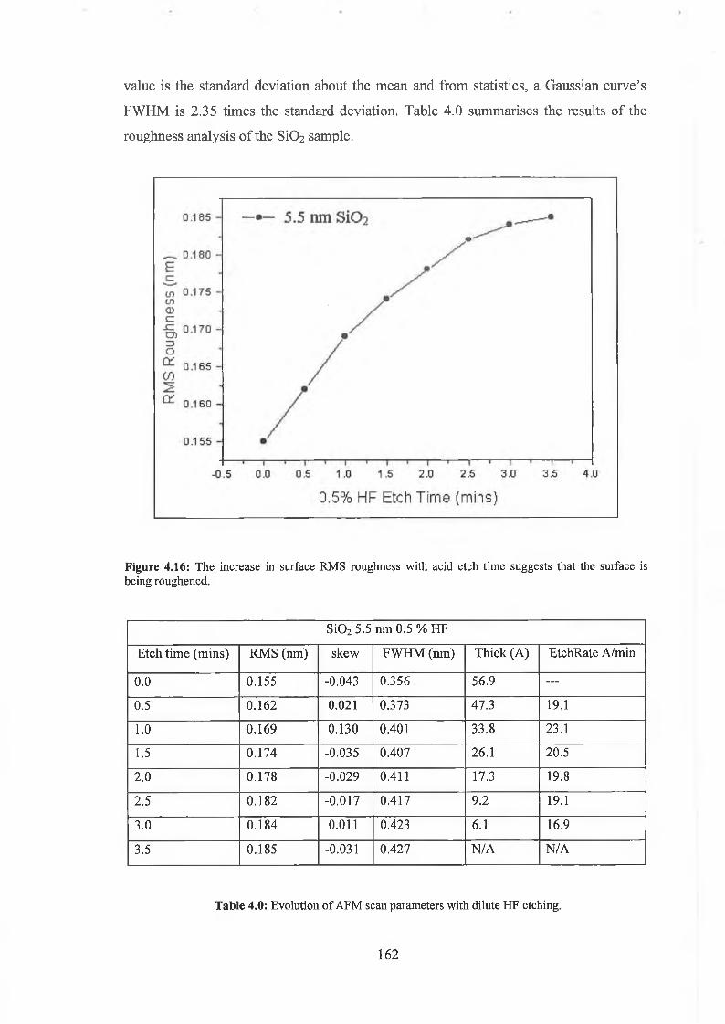
value is the standard deviation about the mean and from statistics, a Gaussian curve’s
FWHM is 2.35 times the standard deviation. Table 4.0 summarises the results of the
roughness analysis of the Si0 2 sample.
Figure 4.16: The increase in surface RMS roughness with acid etch time suggests that the surface is being roughened.
Si02 5.5 nm 0.5 % HF
Etch time (mins) RMS (nm) skew FWHM (nm) Thick (A) EtchRate A/min
0 . 0 0.155 -0.043 0.356 56.9 —
0.5 0.162 0 . 0 2 1 0.373 47.3 19.1
1 . 0 0.169 0.130 0.401 33.8 23.1
1.5 0.174 -0.035 0.407 26.1 20.5
2 . 0 0.178 -0.029 0.411 17.3 19.8
2.5 0.182 -0.017 0.417 9.2 19.1
3.0 0.184 0 . 0 1 1 0.423 6 . 1 16.9
3.5 0.185 -0.031 0.427 N/A N/A
T able 4.0: Evolution o f AFM scan parameters with dilute HF etching.
162
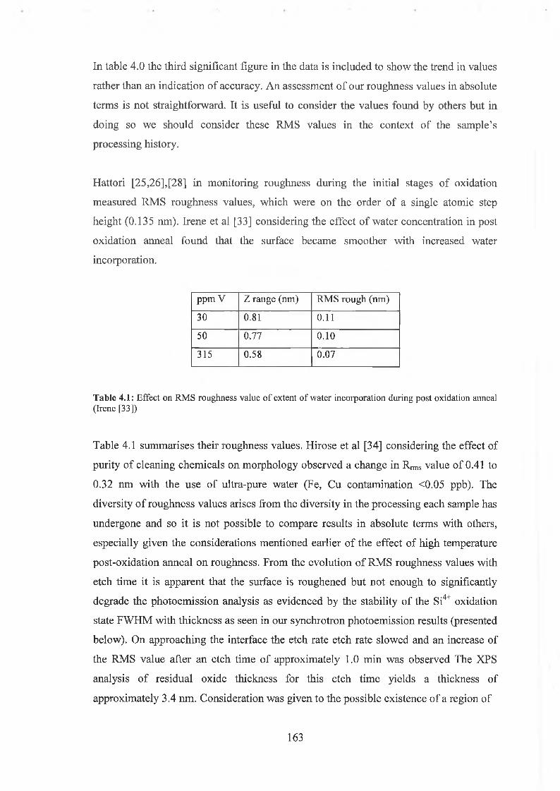
In table 4.0 the third significant figure in the data is included to show the trend in values
rather than an indication of accuracy. An assessment of our roughness values in absolute
terms is not straightforward. It is useful to consider the values found by others but in
doing so we should consider these RMS values in the context of the sample’s
processing history.
Hattori [25,26],[28] in monitoring roughness during the initial stages of oxidation
measured RMS roughness values, which were on the order of a single atomic step
height (0.135 nm). Irene et al [33] considering the effect of water concentration in post
oxidation anneal found that the surface became smoother with increased water
incorporation.
ppm V Z range (nm ) R M S rough (nm )
30 0.81 0.11
50 0.77 0.10
315 0.58 0.07
T able 4.1: Effect on RMS roughness value o f extent of water incorporation during post oxidation anneal (Irene [33])
Table 4.1 summarises their roughness values. Hirose et al [34] considering the effect of
purity of cleaning chemicals on morphology observed a change in Rnns value of 0.41 to
0.32 nm with the use of ultra-pure water (Fe, Cu contamination <0.05 ppb). The
diversity of roughness values arises from the diversity in the processing each sample has
undergone and so it is not possible to compare results in absolute terms with others,
especially given the considerations mentioned earlier of the effect of high temperature
post-oxidation anneal on roughness. From the evolution of RMS roughness values with
etch time it is apparent that the surface is roughened but not enough to significantly
degrade the photoemission analysis as evidenced by the stability of the Si4+ oxidation
state FWHM with thickness as seen in our synchrotron photoemission results (presented
below). On approaching the interface the etch rate etch rate slowed and an increase of
the RMS value after an etch time of approximately 1.0 min was observed The XPS
analysis of residual oxide thickness for this etch time yields a thickness of
approximately 3.4 nm. Consideration was given to the possible existence of a region of
163
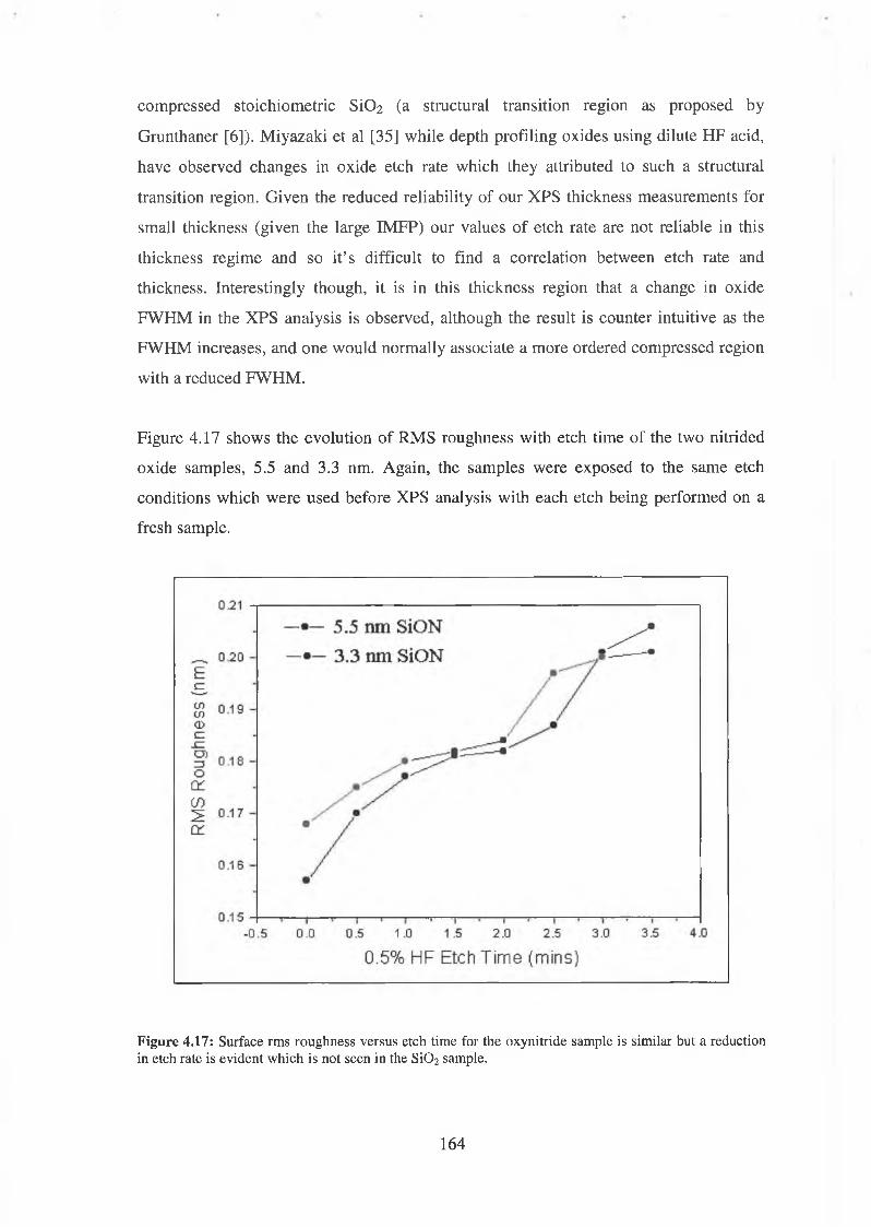
compressed stoichiometric S i0 2 (a structural transition region as proposed by
Grunthaner [6 ]). Miyazaki et al [35] while depth profiling oxides using dilute HF acid,
have observed changes in oxide etch rate which they attributed to such a structural
transition region. Given the reduced reliability of our XPS thickness measurements for
small thickness (given the large IMFP) our values of etch rate are not reliable in this
thickness regime and so it’s difficult to find a correlation between etch rate and
thickness. Interestingly though, it is in this thickness region that a change in oxide
FWHM in the XPS analysis is observed, although the result is counter intuitive as the
FWHM increases, and one would normally associate a more ordered compressed region
with a reduced FWHM.
Figure 4.17 shows the evolution of RMS roughness with etch time of the two nitrided
oxide samples, 5.5 and 3.3 nm. Again, the samples were exposed to the same etch
conditions which were used before XPS analysis with each etch being performed on a
fresh sample.
Figure 4.17: Surface rms roughness versus etch time for the oxynitride sample is similar but a reduction in etch rate is evident which is not seen in the SiC>2 sample.
164
Table 4.2 summarises the roughness parameters.
S iO N 5.5 nm 0.5 % H F SiO N 3.3 nm 0.5 % HF
E tch
tim e
(m ins)
R m s
(nm )
skew F W H
M
(nm )
T hick
(A )
E tchR
ate
A /m in
R m s
(nm )
skew F W H
M
(nm )
T hick
(A)
E tch
R ate
A /m in
0.0 0.157 0.018 0.357 52.4 — 0.168 0.046 0.388 35.3 —
0.5 0.170 -0.023 0.382 40.1 24.6 0.175 -0.023 0.404 25.1 20.4
1.0 0.177 -0 .056 0.399 30.1 22.3 0.180 0.056 0.416 15.5 19.8
1.5 0.181 -0.027 0.416 19.3 22.1 0.182 0.011 0.418 7.5 18.5
2.0 0.182 0.065 0.414 11.7 20.0 0.184 0.032 0.426 4.0 10.4
2.5 0.187 -0.043 0.423 6.0 18.5 0.197 -0.053 0.457 1.7 13.4
3.0 0.201 0.025 0.437 3.0 16.4 0.200 -0.038 0.471 N /A —
3.5 0.206 0.047 0.451 N /A — 0.201 -0.031 0.475 N /A —
Table 4.2: Comparison o f evolution o f AFM scan parameters with HF etching between nitrided and non- nitrided samples.
For both nitrided samples the initial RMS values are larger than the Si0 2 value. The 3.3
nm SiON sample is initially rougher than the 5.5 nm SiON sample. The SiON samples
show an initial rise in roughness followed by a plateau region which is followed by a
final rise which is different from the SiC>2 roughness behaviour. Tallarida et al [36]
investigated the effect on morphology of nitrogen incorporation. He used NO and N20
during post oxidation anneal. He profiled wet chemically through the oxide using dilute
HF and considered the roughness at three stages; no etch (El), a short etch (E2) (which
brought the thickness to within 4 nm of the substrate), and a long etch (E3). Table 4.3
summarises his results. He proposed that in the long etch, the etch process is terminated
when the nitrogen rich interfacial region is reached. He suggested that the change in
etch rate after this time indicated the arrival of the nitrogen rich region in the oxide.
165
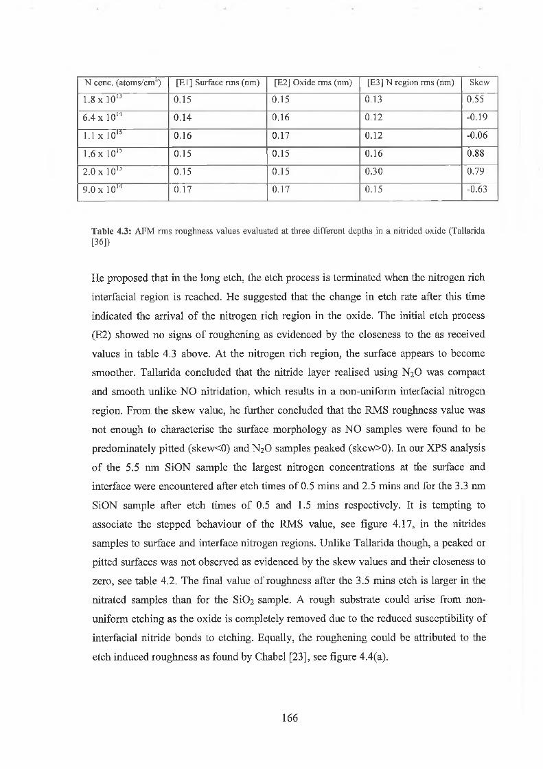
■ 11 —--------------------------------------- m------N conc. (atoms/cm ) [E l] Surface rms (nm) [E2] Oxide rms (nm) [E3] N region rms (nm) Skew
1.8 x 1 0 13 0 .15 0.15 0 .13 0.55
6 .4 x 1 0 14 0 .1 4 0 .16 0 .1 2 -0 .1 9
1.1 x 1 0 15 0 .1 6 0 .17 0 .1 2 -0 .06
1.6 x 1 0 15 0 .15 0 .15 0 .1 6 0.88
2 .0 x 1 0 13 0 .15 0 .15 0 .3 0 0 .79
9 .0 x 1 0 14 0 .1 7 0 .17 0 .15 -0 .63
Table 4.3: AFM rms roughness values evaluated at three different depths in a nitrided oxide (Tallarida [36])
He proposed that in the long etch, the etch process is terminated when the nitrogen rich
interfacial region is reached. He suggested that the change in etch rate after this time
indicated the arrival of the nitrogen rich region in the oxide. The initial etch process
(E2) showed no signs of roughening as evidenced by the closeness to the as received
values in table 4.3 above. At the nitrogen rich region, the surface appears to become
smoother. Tallarida concluded that the nitride layer realised using N20 was compact
and smooth unlike NO nitridation, which results in a non-uniform interfacial nitrogen
region. From the skew value, he further concluded that the RMS roughness value was
not enough to characterise the surface morphology as NO samples were found to be
predominately pitted (skew<0) and N20 samples peaked (skew>0). In our XPS analysis
of the 5.5 nm SiON sample the largest nitrogen concentrations at the surface and
interface were encountered after etch times of 0.5 mins and 2.5 mins and for the 3.3 nm
SiON sample after etch times of 0.5 and 1.5 mins respectively. It is tempting to
associate the stepped behaviour of the RMS value, see figure 4.17, in the nitrides
samples to surface and interface nitrogen regions. Unlike Tallarida though, a peaked or
pitted surfaces was not observed as evidenced by the skew values and their closeness to
zero, see table 4.2. The final value of roughness after the 3.5 mins etch is larger in the
nitrated samples than for the Si0 2 sample. A rough substrate could arise from non-
uniform etching as the oxide is completely removed due to the reduced susceptibility of
interfacial nitride bonds to etching. Equally, the roughening could be attributed to the
etch induced roughness as found by Chabel [23], see figure 4.4(a).
166
Our analysis so far has been obtained from samples etched in dilute HF in order to
gradually and uniformly profile the oxide. In an attempted to gauge the initial surface
morphology, an etch in concentrated HF 49% was performed.
Figure 4.18 (a) and (c) show the height distributions realised by etching a 5.5 nm Si0 2
sample for 15 mins and 0.5 mins in 0.5% HF and 49% HF respectively. Table 4.4
summarises the results. It was found that for a prolonged exposure to dilute acid the
surface became roughened and from the asymmetry in the height distribution was pitted,
as seen in figure 4.18 (A) and the skew value in table 4.2.
E tch T im e (m ins) R M S (nm ) Skew
0.0 [As received] 0.155 0.012
3.3 [0.5% ] 0.18 0.160
15.0 [0.5% ] 0.22 -0.183
0.5 [49% ] 0.16 0.016
T able 4.4: Effect of etch concentration on AFM rms and skew values.
In the XPS analysis an oxide peak could not be detected after a 0.5% HF etch of ~ 3.5
mins and so it was concluded that the acid on removing the oxide begins to roughen the
underlying substrate. After 0.5 min etch in concentrated HF a smooth surface was
uncovered which incidently was rougher than the as-received oxide surface. The RMS
roughness results from the nitrided samples were not consistent. Working with
concentrated HF is difficult because of the handling precautions required.
167
JSIE3.001 (2.0|iin x 2 0|im) :Co.
2.0 urn
SIE1.001 (2.0|im x 2.0iun) :Co... H I h IEJ
SiO? 5.0 mins 0.5% HF
S i O i 0.5 mins 49% HF
Figure 4.18: (a) Height distribution of surface features for dilute 0.5% HF etch for S i0 2 film, (b) Corresponding height mode AFM scan, (c) Height distribution of surface features for concentrated 49%HF etch for S i0 2 film, (d) Corresponding height mode AFM scan.
The data set was not as large for concentrated etches as for dilute etching and because
the attainment of good quality images typically requires several etching attempts the
results were not conclusive. It is interesting to consider to what extent the interface
morphology had evolved from that of the surface in the samples given that they
underwent high temperature anneals and that for the oxynitride samples nitrogen was
incorporated near the interface.168
4.5.1 Discussion o f results
There have been many studies probing the extent of surface and interface roughness and
its relationship to initial surface morphology, chemical treatment, surface orientation,
oxidation temperature and post-oxidation anneal. Given the diversity of the
experimental procedures employed and the fact that some surfaces have been purposely
roughened and some samples partially processed in these studies it is difficult to
compare our results with them. The oxides studied in this thesis have been realised
through a highly optimised industrial process dedicated to oxide uniformity both in
thickness and composition. The quality of the interface is evidenced by the size of the
RMS roughness value of the interface uncovered in the concentrated etch. The
agreement between the interface and surface roughness is encouraging. At 0.5 %
concentration the acid progressively roughens the surface but the extent of the
roughening is not significant enough to undermine our photoemission analysis. When
profiling using ion bombardment we were interested in it only to know if it could realise
controllable depth profiles uniformly. It was found to damage the oxide progressively
but the damage was non-uniform (spatially) and was significant. Analogously, here we
have found wet chemical etching to be progressively damaging but the damage is
uniform spatially (from the skew value) and is not significant enough to undermine the
XPS analysis.
4.6 S i02 Synchrotron Analysis Overview
When the thickness of an oxide is comparable to the sampling depth it is possible to see
the underlying substrate through the oxide and interface. With tuneable photon energy
and high-resolution monochromators, researchers can resolve the overlapping oxidation
states, which greatly aids in the elucidation of interface chemistry. As mentioned
previously, there has been disagreement about the interfacial width and sub-oxide
density with some finding an atomically abrupt chemical transition region consisting of
1.4 ML of suboxides. Others have found a graded interface consisting of 2 ML of
suboxides. In measuring the distribution of oxidation states at the interface there are two
conventional approaches:
169
Firstly for a fixed photon energy, changing the take off angle of the outgoing
photoelectron changes the “effective thickness” being probed as described by equation
d eff = sT ° |a | E quation 4.3
deff is the reduced oxide thickness being probed
dox is the actually oxide thickness
a is the angle between the analyser and the surface plane (i.e. a = 90’ is normal;
small angles are glancing)
The extent of surface sensitivity can be regulated for the same photon energy and the
spatial distribution of the individual oxidation states can be inferred.
In the second approach, for a fixed take off angle the photon energy and hence the
kinetic energy and surface sensitivity of the resulting photoelectrons can be regulated.
The IMFP has a minimum at the photon energy 130 eV [11] for silicon.
Both approaches have limitations. In changing the photoelectron take off angle
consideration needs to be given to photoelectron diffraction effects. In ordered materials
photoemission is anisotropic with large modulations in intensity for photoemission
along crystal axes that correspond to nearest neighbour directions (Bardwell [37]).
Figure 4.19 [37] shows the crystal structure of silicon. At a take-off polar angle of 35°,
the photoelectron trajectory is exactly in line for maximum interaction with a nearest
neighbour, in the [111] direction, a similar maximum interaction at 45° take-off is
expected for the [1 0 1 ] direction.
170
F igure 4.19: The crystal structure for Si, showing the explanation for the relationship between the effects o f photoelectron diffraction at 35° and 45° take-off angles. (Bardwell [37])
Due to the amorphous nature of the Si0 2 oxide, diffraction effects are expected to
average out, and are usually not considered significant. Given the presence of structural
transition regions, the possibility of local crystalline order and the convention of
normalising the oxidation state intensities using the substrate intensity, angular resolved
result should be considered with care. Hattori et al [38] studying photoelectron
diffraction effects in the Si2p photoelectron spectra found that diffraction effects were
not fully smeared out at low oxide thickness. Figure 4.20 (a) shows the azimuthal angle
dependence of the Si2p photoelectrons emitted from a H-Si(l 11) at two take off angles.
The diffraction effect is dependent on both the azimuthal angle and photoelectron take
off angle. Figure 4.20 (b) show the experimental and simulated curves for non-scattered
and elastically scattered Si2p photoelectron signal arising from the substrate.
171
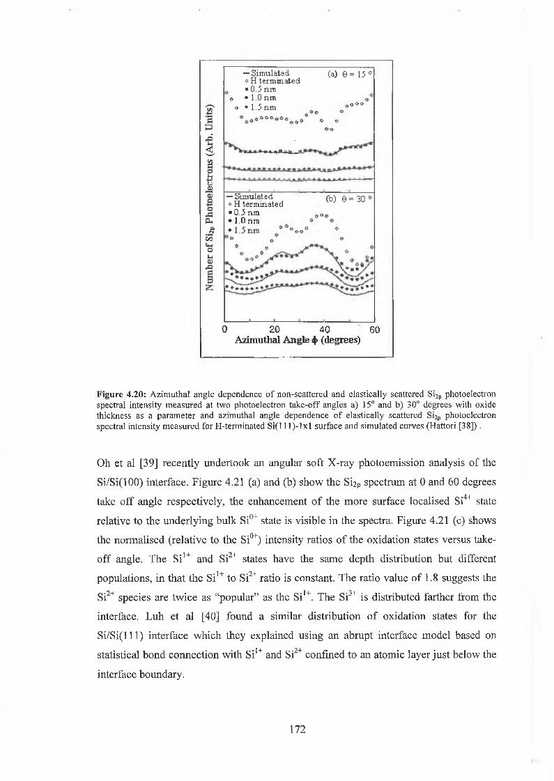
I
Is5tsU£
JhO h
JMi!mO¡HQJpO
— Simulated o H terminated■ O . J 11m
t> *1.011111o *1.5 nm
(a) 6 = 15 0
joao
♦»««»*<
— Simulated o H terminated ■ 0.3 nm • 1.0 nm
(b) 0 = 30 0
0 20 40 60Azimuthal Angle <|> (degrees)
Figure 4.20: Azimuthal angle dependence o f non-scattered and elastically scattered Si2p photoelectron spectral intensity measured at two photoelectron take-off angles a) 15° and b) 30° degrees with oxide thickness as a parameter and azimuthal angle dependence o f elastically scattered Si2p photoelectron spectral intensity measured for H-terminated Si(l 1 l) - lx l surface and simulated curves (Hattori [38]).
Oh et al [39] recently undertook an angular soft X-ray photoemission analysis of the
Si/Si(l 00) interface. Figure 4.21 (a) and (b) show the Si2 P spectrum at 0 and 60 degrees
take off angle respectively, the enhancement of the more surface localised Si4+ state
relative to the underlying bulk Si0+ state is visible in the spectra. Figure 4.21 (c) shows
the normalised (relative to the Si0+) intensity ratios of the oxidation states versus take
off angle. The Si1+ and Si2+ states have the same depth distribution but different
populations, in that the Si1+ to Si2+ ratio is constant. The ratio value of 1.8 suggests the
Si2+ species are twice as “popular” as the Si1+. The Si3+ is distributed farther from the
interface. Luh et al [40] found a similar distribution of oxidation states for the
Si/Si(l 11) interface which they explained using an abrupt interface model based on
statistical bond connection with Si1+ and Si2+ confined to an atomic layer just below the
interface boundary.
172

hv = 130 eV 0 =0° (Normal)
(Grazing)
Emission Angle ( 8 )
K i n e t i c E n e r g y ( f V )
Si4+:(64-x)% Si3:(36+ x)% |g
Figure 4.21: (a) (top) normal emission and (bottom) 60° o ff angle Si2p core-level spectra taken from ultra-thin S i0 2/Si(100) interface oxide, (b) Intensity ratios o f the Si2p oxidation states to the total intensity o f the Si substrate-related components as a function of the polar emission angle (0) (Oh [39]).
Oh [39] however could not explain the existence of the Si3+ state nor the strong take-off• I —angle dependence of the Si state. Instead he proposed a non-abrupt graded interface
model. At least three transition layers are required to explain Oh’s results, see figure
4.21 (c). Si1+ and Si2+ exist only in the first and second layers with a population of (36%
and 64% respectively). Si31 exists in the second and third layers. Using a simple
electron damping model scheme which relates the intensity of each oxidation state to
it’s population in each transition region the solid lines of figure 4.21 (b) were obtained
which agree well with the experimental data (dots) in figure 4.21 (b). Figure 4.21 (d)
173

shows the optimised statistical distribution of each oxidation state in each of the three
transition regions. Other graded interface models have been put forward by Ohdmoari et
[41] al who sought to resolve the density mismatch between Si and Si0 2 through two
transition layers. The difference between Oh’s and Ohdmoari’s results is the distribution• • • • of the Si state. Oh’s results are in disagreement with recent theoretical papers [42,43]
which suggest an abrupt interface model. Unlike Hattori earlier, Oh does not give
consideration to the effects of protrusions or photoelectron diffraction on the
interpretation of his results.
An interesting result in Oh’s Si2p analysis is his inability to obtain a good fit without the
introduction of high and low binding energy peaks (labelled a and P respectively see
figure 4.21(a)) at energies of -0.25 and 0.28 eV relative to the bulk Si0+ peak. He
associated these states with strained Si bonds (not bonded to oxygen) at the termination
of the crystalline substrate. In chapter 3 in the context of Grunthaner’s structural
transition region above the SiOx region, it was mentioned that a structural transition
region is also thought to exist below the interface. Haight and Feldman [44] in a non
destructive study of the interface structure and stoichiometry using ion backscattering
channelling methods (NRA, RBS) found that in the near interfacial region there is a
zone with excess Si, corresponding to non-epitaxial layers within the single crystalline
substrate. They associated the result with a vertical displacement of two atomic layers of
silicon next to the interface.
(a)IDEAL CASE - Si(lOO)
Bulk Si(100) SiOn
1-------------- < *— <
------------------------r . - * —
Ü1] litIli
H - HÍ ! 1
i ---------------» —
S i02* -i ►-
(b)
X X « 'Isf joV X
< X ;o* *
X >
NON-IDEAL CASE - Si(100)
Bulk Si(100)-»4
Dis. SiSiO Si02
» 4 M ►
.a QI X V
¿ . 4 - . « a > > • &T * \ S. A A
— f 1 — v æ 3r > " s \ : < ) ♦ ♦ \ :
Figure 4.22: Illustration o f the theoretical model o f the S i/S i02 interface for an (a) ideal case and (b) realistic case (Atluri [45]).
174

Figure 4.22 shows the Si/Si(100) interface for the “ideal” and the actual case as found
by Atluri et al [45] who examined the disorder of silicon surfaces for various cleaning
conditions (i.e. optimised RAC chemistry) using NRA, ion channelling and AFM. Their
results suggested the existence of unregistered Si atoms below the interface in a
disordered layer, which helps to relieve interfacial strain. These findings are interesting
because many researchers (including ourselves) report FWHM of bulk silicon peaks,
which are larger than Himpsel’s values of 0.28 eV or values typically found for clean Si
surfaces. Next, an account of our soft X-ray photoemission results is given. Suitably
thin oxide thickness were realised from the as-received samples by dilute wet chemical
etching. Angular resolved photoemission measurements were not performed, but instead
have used variable photon energy and etch time to investigate the spatial distribution of
oxidation states at the interface.
4.6.1 Si02 Experimental
Soft X-ray photoemission analysis was performed on beamline U4A at the NSLS. The
beamline includes a 6 m toroidal grating monochromator (TGM), which produces a
photon beam width <0.1 eV resolution at a photon energies of 100-200 eV. The
photoelectron kinetic energy was measured with a VSW 100 mm hemispherical
analyser fixed at 45° to the photon axis. Other details about the beamline are given in
chapter 2. The oxide sample set (as used in XPS analysis chapter 3) consisted of a 5.5
nm Si02, a 5.5 nm and a 3.3 nm SiON oxide. Monochromator number 1 offered the best
resolution for photons in the surface sensitive 120 to 140 eV photon range, which is
ideal for probing the Si2p peak, however the monochromator’s capability spans an
energy window of 10 to 170 eV. It was not possible to access the Cis, Ois or Nis in order
to monitor contamination or examine stoichiometry or chemical shifts. Using a
combined resolution of 150 meV, scans of the Si2p were performed at a pass energy of
10 eY, a step size of 0.05 eY and an integration time of 0.3 sec. These parameters
afforded good signal to noise within a reasonable acquisition time.
All Si2p states were fitted with Voigt functions with 0.1 eV Lorentzian FWHM and
different Gaussian FWHM (taken from Himpsel et al [10]) for each Si2p state, which
were kept fixed during fitting. In all spectra the total width of the Voigt profiles used
175
was dominated by the Gaussian component (typically 90% Gaussian, 10% Lorentzian),
which represent a quadrature sum of the instrumental width (<0.15 eV), the phonon
broadening, and any inhomogeneous disorder broadening. The Lorentzian component
represents the lifetime broadening of the core hole. Fitting was performed using a non
linear least square fit procedure after fitting a fourth order polynomial background. A
branching ratio of 0.5 and spin-orbit splitting of 0.602 eV were used. Samples were
thinned by dilute HF (0.5%) etching followed by rinsing in ultra pure de-ionised water,
and immediate transfer via FEL to UHV (i.e. P< 9xlO" 10 mbar) within 10 minutes,
minimising exposure to surface contamination. Figure 4.23 shows the Si2 P spectrum of a
0.14 nm oxide grown on Si(100) by Himpsel et al [10]. The lower spectrum is the Si2 P3 / 2
component after the subtraction of the smaller Si2Pi/ 2 component from the original
through a numerical spin stripping process after background removal.
Initial-State Energy (eV relative to Ef)
Figure 4.23: Intermcdiate-oxidation states at the S i0 2/Si(100) interface, identified by their Si2p core-level shifts. Top curve is Si2p raw spectra. Bottom curve shows Si2p3/2 component after subtraction of background. All three intermediate oxidation states are seen. For an ideal truncated bulk structure only Si2+ would be present since the Si(100) surface has two broken bonds per atom (Himpsel [10]).
176

Figure 4.24 shows the spectrum of our 5.5 nm Si0 2 sample thinned to 0.13 nm after
etching for 2.5 mins in 0.5% HF. The black line is the experimental data, the red line is
the experimental fit, the background is represented by the dashed line. The individual
Si2P3 / 2 states were fitted to the spin stripped spectrum and are shown in blue.
97 98 99 100 101 102 103 104 105 100
Binding Energy [eV]
Figure 4.24: De-convolution of Si2p spectrum of a 1.3 nm S i0 2 film after background removal and numerically removing the Si2pi/2 component. The spectrum was fitted with four oxidation states as well as two interfacial hydrides. Inset shows a magnified view of intermediate oxidation states.
The peaks SiHi and SiH2 represent interfacia] monohydrides and dihydrides
respectively arising from post oxidation treatment in a H ambient. The inset shows a
magnified (x6 ) view of the hydrides and suboxides with Si0+ and Si4+ states omitted for
clarity. In order to measure the change in surface sensitivity with photon energy, a 5.5
nm Si0 2 oxide was etched to a thickness 0.5 nm, where both the Si0+ and Si4* intensities
were appreciable.
177
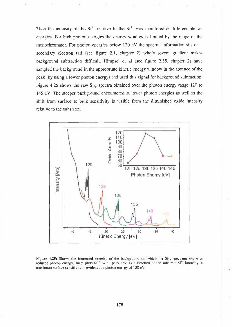
Then the intensity of the Si0+ relative to the Si4+ was monitored at different photon
energies. For high photon energies the energy window is limited by the range of the
monochromator. For photon energies below 120 eV the spectral information sits on a
secondary electron tail (see figure 2 . 1 , chapter 2 ) who’s severe gradient makes
background subtraction difficult. Himpsel et al (see figure 2.35, chapter 2) have
sampled the background in the appropriate kinetic energy window in the absence of the
peak (by using a lower photon energy) and used this signal for background subtraction.
Figure 4.25 shows the raw Si2p spectra obtained over the photon energy range 120 to
145 eV. The steeper background encountered at lower photon energies as well as the
shift from surface to bulk sensitivity is visible from the diminished oxide intensity
relative to the substrate.
Kinetic Energy [eV]
Figure 4.25: Shows the increased severity of the background on which the Si2p spectrum sits with reduced photon energy. Inset plots Si4+ oxide peak area as a function of the substrate Si0+ intensity, a maximum surface sensitivity is evident at a photon energy of 130 eV.
178
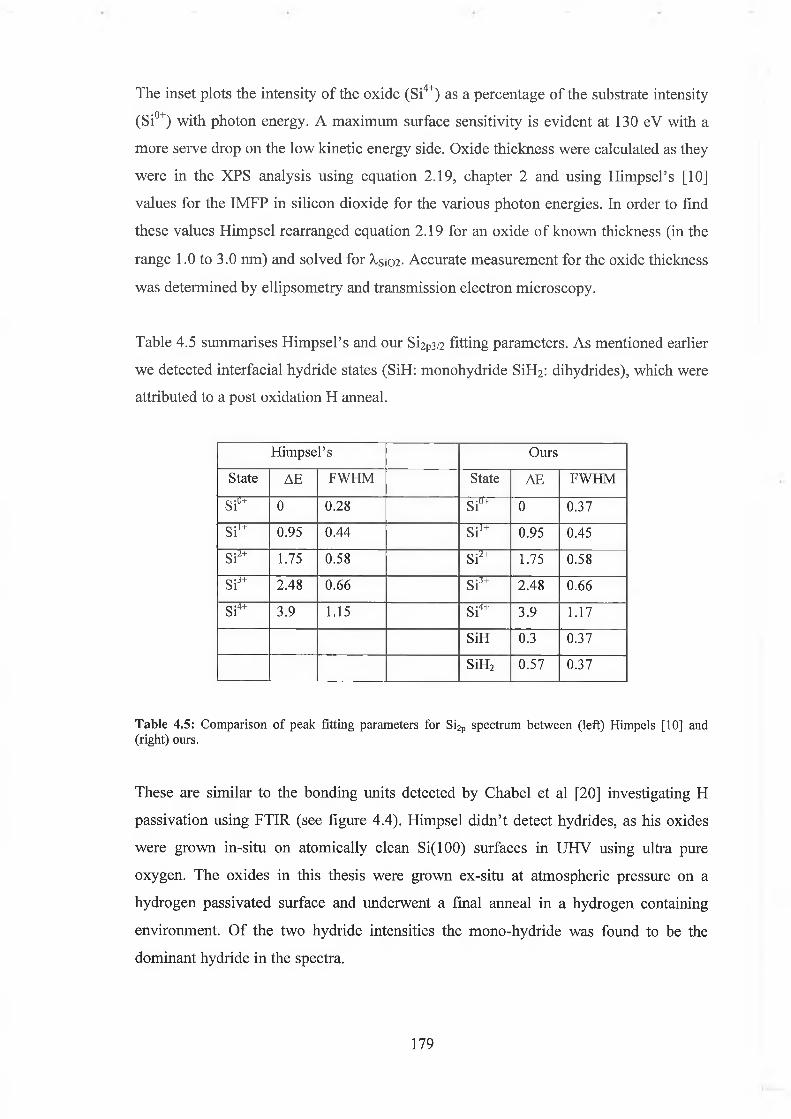
The inset plots the intensity of the oxide (Si4+) as a percentage of the substrate intensity
(Si0+) with photon energy. A maximum surface sensitivity is evident at 130 eV with a
more serve drop on the low kinetic energy side. Oxide thickness were calculated as they
were in the XPS analysis using equation 2.19, chapter 2 and using Himpsel’s [10]
values for the IMFP in silicon dioxide for the various photon energies. In order to find
these values Himpsel rearranged equation 2.19 for an oxide of known thickness (in the
range 1.0 to 3.0 nm) and solved for A,s>02- Accurate measurement for the oxide thickness
was determined by ellipsometry and transmission electron microscopy.
Table 4.5 summarises Himpsel’s and our Si2P3/2 fitting parameters. As mentioned earlier
we detected interfacial hydride states (SiH: monohydride SiH2: dihydrides), which were
attributed to a post oxidation H anneal.
Himpsel’s Ours
State AE FWIIM State AE FWHM
Siu+ 0 0.28 Siu+ 0 0.37
Si1+ 0.95 0.44 SiI+ 0.95 0.45
Si2+ 1.75 0.58 Si2+ 1.75 0.58
SiJ+ 2.48 0.66 Si3+ 2.48 0.66
Si4+ 3.9 1.15 Si4+ 3.9 1.17
SiH 0.3 0.37
SiH2 0.57 0.37
Table 4.5: Comparison o f peak fitting parameters for Si2p spectrum between (left) Himpels [10] and (right) ours.
These are similar to the bonding units detected by Chabel et al [20] investigating H
passivation using FTIR (see figure 4.4). Himpsel didn’t detect hydrides, as his oxides
were grown in-situ on atomically clean Si(100) surfaces in UHV using ultra pure
oxygen. The oxides in this thesis were grown ex-situ at atmospheric pressure on a
hydrogen passivated surface and underwent a final anneal in a hydrogen containing
environment. Of the two hydride intensities the mono-hydride was found to be the
dominant hydride in the spectra.
179
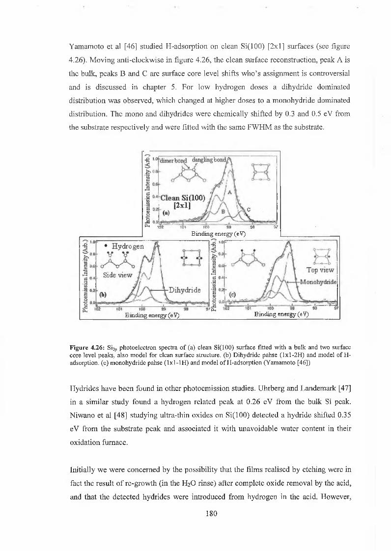
Yamamoto et al [46] studied H-adsorption on clean Si(100) [2x1] surfaces (see figure
4.26). Moving anti-clockwise in figure 4.26, the clean surface reconstruction, peak A is
the bulk, peaks B and C are surface core level shifts who’s assignment is controversial
and is discussed in chapter 5. For low hydrogen doses a dihydride dominated
distribution was observed, which changed at higher doses to a monohydride dominated
distribution. The mono and dihydrides were chemically shifted by 0.3 and 0.5 eV from
the substrate respectively and were fitted with the same FWHM as the substrate.
Figure 4.26: Si2p photoelectron spectra o f (a) clean Si(100) surface fitted with a bulk and two surface core level peaks, also model for clean surface structure, (b) Dihydride pahse (lx l-2 H ) and model of H- adsorption. (c) monohydride pahse ( lx l- lH ) and model of H-adsorption (Yamamoto [46])
Hydrides have been found in other photoemission studies. Uhrberg and Landemark [47]
in a similar study found a hydrogen related peak at 0.26 eV from the bulk Si peak.
Niwano et al [48] studying ultra-thin oxides on Si(100) detected a hydride shifted 0.35
eV from the substrate peak and associated it with unavoidable water content in their
oxidation furnace.
Initially we were concerned by the possibility that the films realised by etching were in
fact the result of re-growth (in the H2O rinse) after complete oxide removal by the acid,
and that the detected hydrides were introduced from hydrogen in the acid. However,
Jm 0 0-.V ( ' —— ~-P-1 102 " lOi IM ~ 90 97
B in d in g e n e rg y (eV)
Binding energy (eV)_________________________ Binding energy (eV)
180

Yamamoto’s [46] studies of oxide re-growth on hydrogen passivated Si(100) show
films whose structure is poor and are so thin that peak assignment is unrealistic. The
oxides studied in this thesis however, are well defined and are of a comparable quality
to those grown to similar thickness in UHV environments. Great care was taken to
ensure as constant a time as possible elapsed between chemical treatment and analysis.
Therefore the ability to realise precisely thinner films, with precisely longer etch times
would have been seriously undermined by re-growth during chemical treatment which if
responsible would have lead to a random distribution of oxide thickness. Figure 4.27
shows a SÍO2 sample etched for 10 mins followed by 10 min immersion in deionised
water.
Binding Energy [eV]
Figure 4.27: Si02 Si2p spectrum showing interfacial hydrides in green and orange.
The mono and dihydride peaks are highlighted in green and orange respectively.
Effectively no oxide re-growth is evident here eliminating the possibility of the other
etched oxides (which were etched for shorter times!) arising from growth during
preparation. Also Tay et al [49-52] (see figure 3.4, chapter 3) have successfully
performed numerous photoemission studies (both monochromated and synchrotron) of
181
ultra-thin oxides realised by dilute HF etch back and have not reported the presence of
hydrides.
Table 4.5 shows good agreement between our fitting parameters and Himpsel’s [10],
except for the value of FWHM of the Si substrate peak (Si0+). Other researchers [39]
[53] in soft X-ray studies (at the photon energy 130 eV) have mentioned the need to
introduce extra peaks near the substrate peak in order to achieve a good fit or the need
for a larger FWHM. Keister et al [53] used a value of 0.36 eV, which agrees well with
our value of 0.37 eV. Lu et al [40] used a value as large as 0.41 eV. As mentioned
earlier, these larger values of FWHM have been associated with strained interfacial
silicon below the interface who’s spectral contribution cannot be easily resolved from
the Si0+ peak due to finite resolution and in our case the added presence of overlapping
hydrides.
4.6.2 Interface state distribution
In calculating the oxide thickness, the sample was treated (using the overlayer model) as
a thin oxide sitting on an infinite substrate and equation 2.19.
d = Ln 1 S iO 2 Ip ^
1« I .Xsio Equation 2.19
dsi02 is the oxide thickness
Isi02 and Isj are the photoelectron signals from the oxide and substrate respectively
X sio2 is the IEMFP in the oxide
Io is the signal from a clean silicon substrate
1«, is the signal from an infinitely thick oxide
In order to calculate the density of suboxide species the suboxide region was treated as a
thin film of thickness dox sitting on an infinite substrate. Equation 2.19 was re-arranged
to get equation 4.4:
182
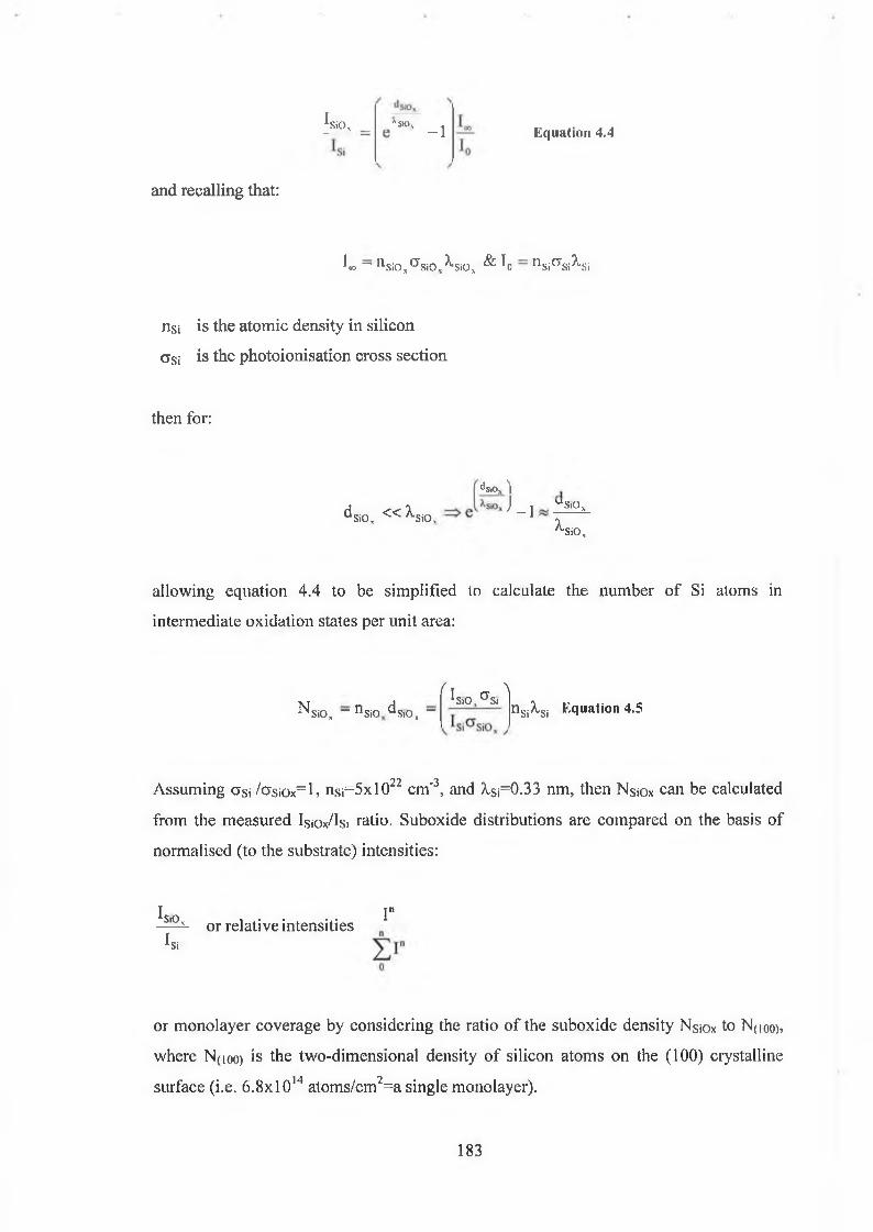
SiO' ■Vi I«., -1 Equation 4.4
and recalling that:
1=0 ~ n S i0x i7 S i0 5^ 'S i0 x &Ifl n S i° rSi^'Si
nsi is the atomic density in silicon
CTsi is the photoionisation cross section
then for:
SiO, <<: ^SiO.
dSiO, ]J _ J u -SiC\
SiO,
allowing equation 4.4 to be simplified to calculate the number of Si atoms in
intermediate oxidation states per unit area:
Nsio, - nsio ^sio, —f r A
*SiO, CTSi n sjA,Sj Equation 4.5
Assuming asi /cysiOx= l, nsp 5 x l0 22 cm'3, and ^¡=0.33 nm, then NsiOx can be calculated
from the measured Isiox/Isi ratio- Suboxide distributions are compared on the basis of
normalised (to the substrate) intensities:
I I"Sl°* or relative intensities ——I*
or monolayer coverage by considering the ratio of the suboxide density NsiOx to N(ioo),
where N(ioo> is the two-dimensional density of silicon atoms on the ( 100) crystalline
surface (i.e. 6 .8x l0 H atoms/em2=a single monolayer).
1 8 3
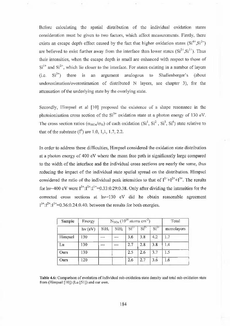
Before calculating the spatial distribution of the individual oxidation states
consideration must be given to two factors, which affect measurements. Firstly, there
exists an escape depth effect caused by the fact that higher oxidation states (Si4+,Si3+)• 2+ • 1“Fare believed to exist further away from the interface than lower states (Si ,Si ). Thus
their intensities, when the escape depth is small are enhanced with respect to those of
SiI+ and Si2+, which lie closer to the interface. For states existing in a number of layers
(i.e. Si3+) there is an argument analogous to Shallenberger’s (about
underestimation/overestimation of distributed N layers, see chapter 3), for the
attenuation of the underlying state by the overlying state.
Secondly, Himpsel et al [10] proposed the existence of a shape resonance in the
photoionisation cross section of the Si3+ oxidation state at a photon energy of 130 eV.
The cross section ratios (crsiOx/tfsi) ° f each oxidation (Si1, Si2 , Si3, Si4) state relative to
that of the substrate (1°) are 1.0, 1,1, 1.7, 2.2.
In order to address these difficulties, Himpsel considered the oxidation state distribution
at a photon energy of 400 eV where the mean free path is significantly large compared
to the width of the interface and the individual cross sections are nearly the same, thus
reducing the impact of the individual state spatial spread on the distribution. Himpsel
considered the ratio of the individual peak intensities to that of I1++I2++I3+. The results
for hv=400 eV were I3+:I2+:I1+=0.33:0.29:0.38. Only after dividing the intensities for the
corrected cross sections at hv=130 eV did he obtain reasonable agreement
I3+:I2+:I1+=0.36:0.24:0.40. between the results for both energies.
Sample Energy Nsiox (1014 atoms cm'2) Total
hv (eV) SiH] SiH2 Si Si2+ Si monolayers
Himpsel 130 — — 3.6 3.8 4.2 1.7
Lu 130 — — 2.7 2.8 3.8 1.4
Ours 130 2.5 2.6 3.7 1.5
Ours 120 2.6 2.7 3.6 1.6
Table 4.6: Comparison o f evolution o f individual sub-oxidation state density and total sub-oxidation state from (Himpsel [10]) (Lu [51]) and our own.
184

However, there has been some disagreement about the correction values. Rochet et al
[55] observed an enhancement of the Si4+and Si3+ states relative to the Si,+ state of
+45%, +20% respectively compared to Himpsel’s values of 120% and 6 6 %. Table 4.6
compares our results for interface suboxide density with Himpsel’s and Lu’s. Our
results are based on the intensities of a 1.3 nm oxide realised by etching our 5.5 nm
Si02 sample for 2.5 mins in 0.5% HF, see figure 4.24. This is an optimal thickness
because for thicker oxides it isn’t possible to “see” the substrate peak well enough to fit
it and for thinner oxides part of the chemical transition region may be partially removed.
In calculating the total sub-oxide density we included the contribution from both
hydrides and Himpsel’s cross-section corrections. The calculated value of total interface
state density obtained was between that of Himpsel’s and Lu’s. Our results for the
“deeper” illumination of 120 eV give a larger value of suboxide density than those at
130 eV. This was attributed to the “escape depth” effect and the possible inaccuracy of
Himpsel’s correction values for the cross sections at hv=130 eV, as discussed below.
Our value of 1.5 monolayers of interface suboxide is relatively small. This is attributed
to the post oxidation anneal treatment. Keister et al [53] who investigated the effect of
post oxidation anneal temperature on S i(lll) /S i0 2 suboxide interface state density
found a 15% to 20% reduction with anneal temperature from 700°C to 900°C.
Temp °C N, (ML) N2 (ML) N3 (ML) EN, (ML)
300 0.87 0.59 0.38 1.84
700 0.92 0.26 0.42 1.60
800 0.82 0.23 0.58 1.63
900 0.79 0.30 0.46 1.56
Table 4.7: Evolution o f individual sub-oxidation oxidation state density and total sub-oxidation state density with post oxidation anneal temperature (Keister [53])
Table 4.7 summarises their results. I3+ and I1+ remain relatively constant with annealing,
however, the non-intrinsic I2+ feature is significantly reduced. Keister’s final interface
state density is 13% lower than Himpsel’s.
185
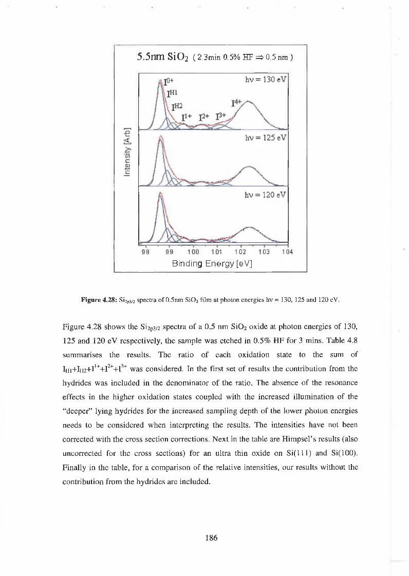
5.5nm Si02 ( 2.3min 0.5% HF =>0 5 nm )
Binding Energy [eV]
Figure 4.28: Si2p3/2 spectra of 0.5nm S i0 2 film at photon energies hv = 130, 125 and 120 eV.
Figure 4.28 shows the Si2P3/2 spectra of a 0.5 nm SiC>2 oxide at photon energies of 130,
125 and 120 eV respectively, the sample was etched in 0.5% HF for 3 mins. Table 4,8
summarises the results. The ratio of each oxidation state to the sum of
Ihi+Ih2+I1++I2++I3+ was considered. In the first set of results the contribution from the
hydrides was included in the denominator of the ratio. The absence of the resonance
effects in the higher oxidation states coupled with the increased illumination of the
“deeper” lying hydrides for the increased sampling depth of the lower photon energies
needs to be considered when interpreting the results. The intensities have not been
corrected with the cross section corrections. Next in the table are Himpsel’s results (also
uncorrected for the cross sections) for an ultra thin oxide on S i( l l l) and Si(100).
Finally in the table, for a comparison of the relative intensities, our results without the
contribution from the hydrides are included.
186

An interpretation of the results in terms of the spatial distribution is difficult for the
following reasons:
• When illuminating the outer surface using surface sensitive hv=130 eV photon
energy, it is tempting to attribute the enhanced signal from the higher oxidation
states to their distribution being further away from the interface. However, one
must consider the influence of the resonance in the cross section.
• When illuminating deeper into the surface using the more bulk sensitive hv=120
eV photon energy it is tempting to interpret the enhanced hydride signal as
arising from the interfacial region and that this signal was underestimated at
hv=130 eV.
In order to address this difficulty, Himpsel compared his surface sensitive results with
those obtained using the more bulk sensitive photon energy hv=400 eV where the
effects of cross section resonance and escape depth are negligible. Having corrected for
the cross section he found good agreement for the results at 130 and 400 eV. However,
Rochet [55] have found Himpsel’s corrections to be overestimated and have even found
the photoionisation cross-section resonance to occur at 135 eV instead of 130 eV.
The ratios for our intensities after correction using Himpsel’s cross-section values are
shown in table 4.8 in red beside the uncorrected values. These data suggest that
Himpsel’s corrections over estimate the cross sections for the Si2+ and Si3+ states at
hv=130 eV. If the ratios at hv=125 and 120 eV are considered, where the resonance
effect is absent, then the Si3+ signal is reduced for the deeper illumination of 120
relative to 125 eV. The interpretation of the hydride behaviour is less straightforward.
The increased hydride signal with deeper illumination at 120 eV compared to 125 eV
and 130 eV could be attributed to the escape depth effect because the hydrides are
localised at the interface and so are not fully illuminated at the more surface sensitive
photon energies. One would also expect the indigenous Si2+ state to show a comparable
increase because it is expected to be localised at the interface. It is likely therefore from
the hydride intensity behaviour that they are to some extent distributed both below the
interface and in the interfacial region.
187
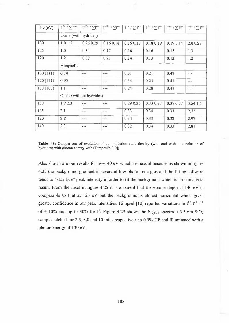
hv (eV) r / £ r IH,+ / ZIn+ !H2' / i r i1+ / x r + j2+1 £ f+ I3+ / 1 r I4+ / 1 f +
Our’s (with hydrides)
130 1.0 1.2 0.26 0.29 0.160.18 0.16 0.18 0.18 0.19 0.19 0.14 2.0 0.27125 1.0 0.34 0.17 0.16 0.16 0.15 1.3120 1.2 0.37 0.21 0.14 0.13 0.13 1.2
Himpsel’s
130(111) 0.74 — — 0.31 0.21 0.48 —
1 2 0 (111) 0.95 — — 0.34 0.25 0.41 —
130(100) 1.1 — — 0.24 0.28 0.48 —
Our’s (without hydrides)
130 1.9 2.3 — — 0.29 0.36 0.33 0.37 0.37 0.27 3.54 1.6
125 2.1 — — 0.33 0.34 0.33 2.72
120 2.8 — — 0.34 0.33 0.32 2.97
140 2.3 — — 0.32 0.34 0.33 2.81
Table 4.8: Comparison o f evolution o f our oxidation state density (with and with out inclusion of hydrides) with photon energy with (Himpesl’s [10])
Also shown are our results for hv=140 eV which are useful because as shown in figure
4.25 the background gradient is severe at low photon energies and the fitting software
tends to “sacrifice” peak intensity in order to fit the background which is an unrealistic
result. From the inset in figure 4.25 it is apparent that the escape depth at 140 eV is
comparable to that at 125 eV but the background is almost horizontal which gives
greater confidence in our peak intensities. Himpsel [10] reported variations in I1+:I2+:I3+
of ± 10% and up to 30% for 1°. Figure 4.29 shows the Si2P3/2 spectra a 5.5 nm SiC>2
samples etched for 2.5, 3.0 and 10 mins respectively in 0.5% HF and illuminated with a
photon energy of 130 eV.
188
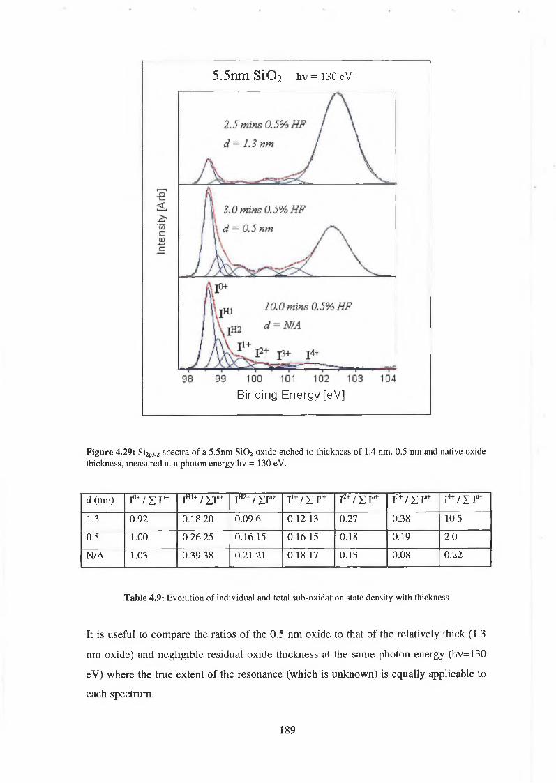
5.5nm SiO hv = i30eV
Binding Energy [eV]
Figure 4.29: Si2p3/2 spectra of a 5.5mn SiC>2 oxide etched to thickness of 1.4 nm, 0.5 nm and native oxide thickness, measured at a photon energy hv = 130 eV.
d (nm) I°+1 £ jn+ iH1+/ i r IH2+ / I I n+ i1+/ z r I2+ / 1 In+ i3+/ z r + r / 1 r ,+
1.3 0.92 0.18 20 0.09 6 0.12 13 0.27 0.38 10.5
0.5 1.00 0.26 25 0.16 15 0.16 15 0.18 0.19 2.0
N/A 1.03 0.39 38 0.21 21 0.18 17 0.13 0.08 0.22
Table 4.9: Evolution of individual and total sub-oxidation state density with thickness
It is useful to compare the ratios of the 0.5 nm oxide to that of the relatively thick (1.3
nm oxide) and negligible residual oxide thickness at the same photon energy (hv=130
eV) where the true extent of the resonance (which is unknown) is equally applicable to
each spectrum.
189
The dominance of the Si3+ state in the suboxide distribution for the thicker sample is
consistent with our expectation that it is localised away from the interface. Also, the Si,+
state is more prominent in the thinner oxide. Shown in red in table 4.10 are the hydride
intensities as a percentage of the substrate intensity. The increased signal from the
hydrides (relative to the substrate) with deeper illumination and for thinner samples, and
the change in intensity of the dihydride as a percentage of the mono hydride as shown in
table 4.10 was an unexpected resulted as both hydrides were expected to be equally
localised near the interface.
d (nm ) Si % ( Si )
1.3 22
0.5 54
N / A 62
Table 4.10: Dihydride intensity as a percentage o f monohydride intensity.
The data suggests that both hydrides are present at the interface. The dihydride state is
strongly localised at the interface because of its role as a passivator of the indigenous
dangling bond state. The monohydride is distributed through the suboxide region
because of the greater bonding opportunities for a monohydride state. The results
obtained are expressed qualitatively below in figure 3.30 where the suboxide layer is
sandwiched between an amorphous Si02 and crystalline Si layer. Although not
supported by the data, a strained layer of S i02 is incorporated into figure 4.30. The
individual sub oxidation states are identified by colour. Given the complexity of the
bonding geometry figure 4.30 is unable to convey micro structural information, instead
its purpose is to convey the spatial distribution and population of the various sub
oxidation states across the SiOx region. Therefore, similar to Oh [39] et al (see figure
4.21) it is reasonable to suppose that the SiOx region is distributed with individual
oxidation states populating different layers of the SiOx region compounding the escape
depth effect outlined by Himpsel et al [10].
190
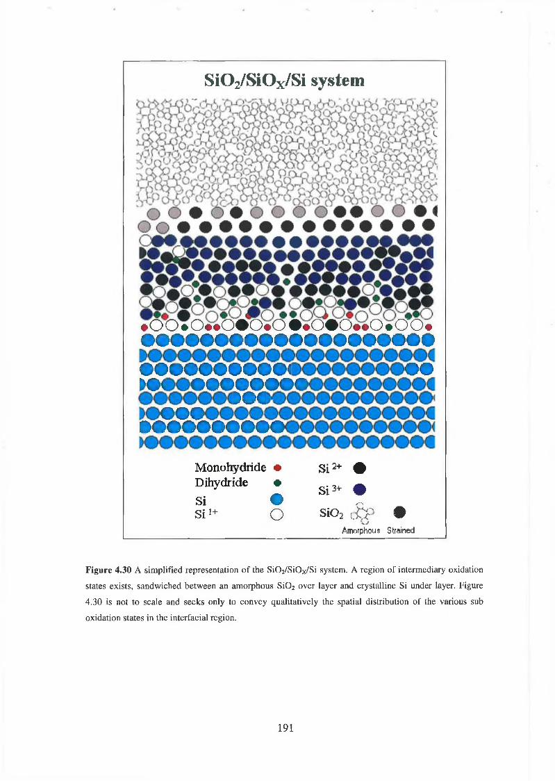
Si02/S i0x/Si system
•O o • o**o#o*o ••o#o**o «00» © © @ © © ® © ® © ® @ ® © ® ® © @ ® € > € >
OOOOOOOOOOi o oXX OOOQOOOO
3 C C ' . 'O O O ' ' '
> ® ® ® ® ® ® —
Monohydride • S i2+ #Dihydride • s i 3+ •Si ^s i 1+ o s i ° 2 ( .& ' •
v->Amorphous Strained
Figure 4.30 A simplified representation of the S i0 2/Si0x/Si system. A region of intermediary oxidation
states exists, sandwiched between an amorphous S i0 2 over layer and crystalline Si under layer. Figure
4.30 is not to scale and seeks only to convey qualitatively the spatial distribution of the various sub
oxidation states in the interfacial region.
191

4.6.3 Discussion of results
The chemical shifts of the intermediate sub-oxidation states and their relative intensities
agree very well with the values reported in the literature [10],[51]. The low value of
interface suboxide density of 1.5 monolayers affirms the interface quality. Lower values
have been achieved experimentally [53]. However, given that the dielectric layers
studied in this thesis have undergone post oxidation treatment and given the presence of
interfacial hydrides it is reasonable that the interface is more distributed due to this
processing. This distribution of suboxide states was investigated by variation of photon
energy for a fixed thickness. The Si+1, Si+2 states were found to be interface localised
and the Si3+ was located further out into the oxide. The validity of this result has to be
considered in the context of the undermining effects of: overestimation of higher
oxidation states due to resonance in photoionisation cross section and escape depth
effects. The gradual removal rate of dilute HF acid allowed the interfacial region to be
depth profiled without changing the photon energy. The same trend in the localisation of
the individual sub-oxidation states as mentioned above adds weight to the view that the
interface is not abrupt but is graded as described by Oh et al [39].
Monohydride and dihydride states were consistently fitted in the interfacial region. The
behaviour of the hydride peak intensities with thickness in the near interfacial region
suggested that the dihydride peak was localised near the interface. Its role at the
interface is in quenching the indigenous (two broken bond per surface atom) Si(100)
surface state. The monohydride state appears to be more distributed throughout the
interfacial region. It is possible that H plays a role in passivating other defects.
The photoemission analysis of the Si0 2 /Si(1 0 0 ) interface has provided a template of
peak chemical shifts and intensity distributions against which the photoemission results
of the SiON/Si(100) results can be compared in order to elucidate the presence of
interfacial nitrogen.
192
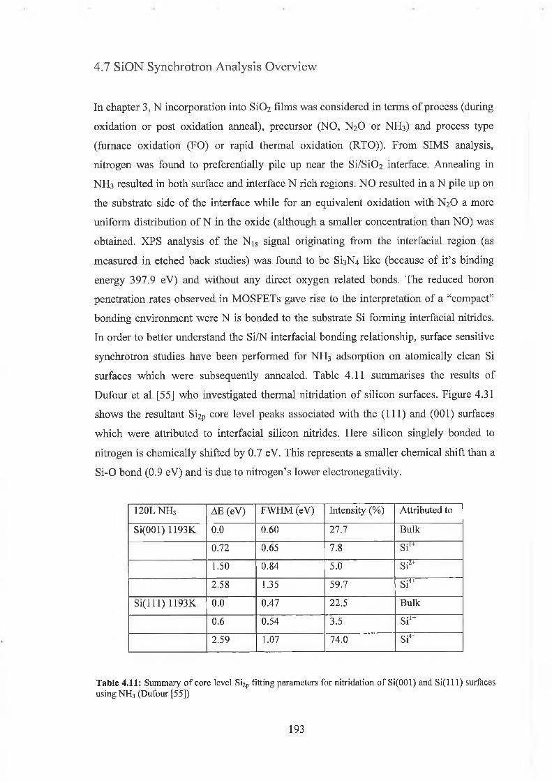
4.7 SiON Synchrotron Analysis Overview
In chapter 3, N incorporation into S i02 films was considered in terms of process (during
oxidation or post oxidation anneal), precursor (NO, N20 or NH3) and process type
(furnace oxidation (FO) or rapid thermal oxidation (RTO)). From SIMS analysis,
nitrogen was found to preferentially pile up near the Si/Si02 interface. Annealing in
NH3 resulted in both surface and interface N rich regions. NO resulted in a N pile up on
the substrate side of the interface while for an equivalent oxidation with N20 a more
uniform distribution of N in the oxide (although a smaller concentration than NO) was
obtained. XPS analysis of the N is signal originating from the interfacial region (as
measured in etched back studies) was found to be Si3N4 like (because of it’s binding
energy 397.9 eV) and without any direct oxygen related bonds. The reduced boron
penetration rates observed in MOSFETs gave rise to the interpretation of a “compact”
bonding environment were N is bonded to the substrate Si forming interfacial nitrides.
In order to better understand the Si/N interfacial bonding relationship, surface sensitive
synchrotron studies have been performed for NH3 adsorption on atomically clean Si
surfaces which were subsequently annealed. Table 4.11 summarises the results of
Dufour et al [55] who investigated thermal nitridation of silicon surfaces. Figure 4.31
shows the resultant Si2P core level peaks associated with the (1 1 1 ) and (0 0 1 ) surfaces
which were attributed to interfacial silicon nitrides. Here silicon singlely bonded to
nitrogen is chemically shifted by 0.7 eV. This represents a smaller chemical shift than a
Si-0 bond (0.9 eV) and is due to nitrogen’s lower electronegativity.
1 2 0 L N H 3 AE (eV) FWHM (eV) Intensity (%) Attributed to
Si(001) 1193K 0.0 0.60 27.7 Bulk
0.72 0.65 7.8 S iI+
1.50 0.84 5.0 Si2+
2.58 1.35 59.7 Si4+
S i ( l l l ) 1193K 0.0 0.47 22.5 Bulk
0.6 0.54 3.5 Si1+
2.59 1.07 74.0 Si4+
Table 4.11: Summary o f core level Si2p fitting parameters for nitridation o f Si(001) and Si(l 11) surfaces using NH3 (Dufour [55])
193

Figure 4.31: Si2p3/2 fits for (top) Si(100) and (bottom) S i ( l l l ) surfaces after thermal nitridation. Fitting parameters are shown in table 4.11 (Dufour [55])
Similar to the Si/SiC>2 interface the chemical shift of 0.7 eV is considered additive.
Dufour [55] considered the interface as bulk crystalline Si connected to a disordered
Si3N4 lattice. An ideal SiaWSiCOOl) interface should exhibit only the Si2+ state, the
presence of the Si1+ state excluded the possibility of an abrupt interface. However, given
the presence of the Si4+ (stoichiometric silicon nitride Si3N4) and Si1+ state for the
Si3N4/Si(l 11) interface it is closer to the ideal interface. Similar studies were performed
by Bishoff et al [56] and Peden et al [57].
These studies are useful in that they provide an expectation of the chemical shifts and
intensity distributions associated with nitrogen bonding to the substrate similar to O
adsorption studies on clean silicon surfaces. The expectation that interfacial N bonds to
the substrate is influenced by SIMS results which reveal the location of nitrogen to be at
the interface, and in the case of NO annealed samples below the interface in the
substrate silicon as found by Hedge et al [58] and from the XPS Nis binding energy
being Si3N4 like. Recently Garfunkel et al [59] using MEIS (which offers better spatial
194
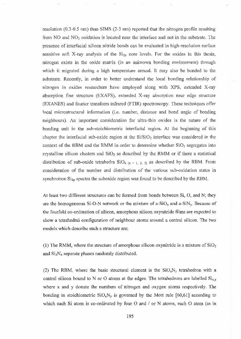
resolution (0.3-0.5 nm) than SIMS (2-3 nm) reported that the nitrogen profile resulting
from NO and N 0 2 oxidation is located near the interface and not in the substrate. The
presence of interfacial silicon nitride bonds can be evaluated in high-resolution surface
sensitive soft X-ray analysis of the Si2P core levels. For the oxides in this thesis,
nitrogen exists in the oxide matrix (in an unknown bonding environment) through
which it migrated during a high temperature anneal. It may also be bonded to the
substrate. Recently, in order to better understand the local bonding relationship of
nitrogen in oxides researchers have employed along with XPS, extended X-ray
absorption fine structure (EXAFS), extended X-ray absorption near edge structure
(EXANES) and fourier transform infrared (FTIR) spectroscopy. These techniques offer
local microstructural information (i.e. number, distance and bond angle of bonding
neighbours). An important consideration for ultra-thin oxides is the nature of the
bonding unit in the sub-stoichiometric interfacial region. At the beginning of this
chapter the interfacial sub-oxide region at the Si/Si02 interface was considered in the
context of the RBM and the RMM in order to determine whether Si02 segregates into
crystalline silicon clusters and Si02 as described by the RMM or if there a statistical
distribution of sub-oxide tetrahedra SiOx (x = i ; 2, 3) as described by the RBM. From
consideration of the number and distribution of the various sub-oxidation states in
synchrotron Si2p spectra the suboxide region was found to be described by the RBM.
At least two different structures can be formed from bonds between Si, O, and N; they
are the homogeneous Si-O-N network or the mixture of a-SiOx and a-SiNy. Because of
the fourfold co-ordination of silicon, amorphous silicon oxynitride films are expected to
show a tetrahedral configuration of neighbour atoms around a central silicon. The two
models which describe such a structure are;
(1) The RMM, where the structure of amorphous silicon oxynitride is a mixture of Si02
and Si3N4 separate phases randomly distributed.
(2) The RBM, where the basic structural element is the SiOxNy tetrahedron with a
central silicon bound to N or O atoms at the edges. The tetrahedrons are labelled Six>y
where x and y donate the numbers of nitrogen and oxygen atoms respectively. The
bonding in stoichiometric SiOxNy is governed by the Mott rule [60,61] according to
which each Si atom is co-ordinated by four O and / or N atoms, each O atom (as in
195

Si02) is co-ordinated by two silicon atoms and each N atom is co-ordinated by three Si
(as in Si3N4) or O atoms. Each bond between Si and N or O follows a stochastic law and
according to Phillips [62] the distribution Hz(x,y) of tctrahedra with stoichiometries Siz
defined by (x+y=z), (x=z, y=4-z) is given by equation 4.6 which is similar to the
distribution of SiC>4 tetrahedrons in stoichiometric Si02 given by equation 4.0.
H z = f 2 x 'f n \
y
i „ . 4 ! )
^ 2 x + 3 _ y , k 2 x + 2>
1t-
1
N
Equation 4.6
In stoichiometric SiOxNy the central silicon atom is fourfold co-ordinated. The two fold
co-ordinated oxygen atom bridges two silicon atoms and has a bonding angle that varies
between 120° and 180°. This oxygen is the most variable structural element in SiOxNy.
In a-Si3N4, nitrogen is three fold co-ordinated and builds plane triangles with silicon, a
more rigid structure compared to the oxygen bridge.
By depositing silicon oxynitride films of various stoichiometries (as discussed above)
using techniques such as plasma enhanced chemical vapor deposition (PECVD) and
thermal low pressure chemical vapor deposition (LPTCYD) researchers have attempted
to characterise the various bond geometries that exist in thin S i02 samples after N
incorporation in order to better understand the resultant chemical states and their
relation with stoichiometric and structural changes.
Behrens et al [63] who studied the whole range of possible compositions of SiOxNy
films deposited on Si(100) concluded that the bonding network of silicon oxynitrides
can be described by a mixture of the RBM and the RMM. For low oxygen contents
(x/(x+y)<0.3), the geometric structure of the film is almost the structure of a-SiaN4, with
the oxygen preferably on top of the Si-N3 triangles building Sii3 tetrahedrons, which is
the basic structural element of Si2N20 . As the oxygen concentration increases the O is
forced into the triangle and mixed tetrahedrons like Si2i2 dominate the structure.
Gritsenko et al [64] using LPCVD deposited a-SiOxNy and SiNx films on Si(100). They
considered the partial charge on a central silicon atom in a tetrahedron due to its
neighbours using Sanderson electronegativities and the calculated Si2p chemical shift for
the various tetrahedral stoichiometries.
196
They concluded from the agreement between modelled and experimental XPS data that
the distribution of a-SiOxNy bonding unit is described by the RBM and the distribution
of deposited SiNx stoichiometricies is described by the RMM as SiNx species dissociate
into SiaN4 and Si clusters.
Scopel et al [65] characterised SiOxNy:H films deposited by PECVD. Using XANES,
EXAFS, FTIR and RBS they compared the film’s properties to those of reference
materials (i.e. a-SiC>2 and pSi3N4), and concluded that bonding tetrahedra are best
described using the RBM and that for low nitrogen concentrations the films properties
are close to those of a-SiC>2.
The local geometric bonding structure of the oxynitrides studied in this thesis is of
interest for the following reasons. From XPS analysis nitrogen was shown to exist in the
films. From wet chemical depth profiles nitrogen was found in the near surface and
interfacial region of the oxide. An asymmetric Nis peak was found. The extent of the
asymmetry depended on thickness, which was attributed to a second phase of (Si3N4
like) N which is affected by second nearest neighbour oxygens in accordance with the
findings of Shallenberger [6 6 ] and Bouvet [67]. N -0 related bonds were not detected
and (as will be discussed below) the interfacial Si-N bonding was not attributed to
nitrogen bonded to substrate silicon. These observations suggest the existence of a Si3N4
like bonding unit in the oxide for which either the stoichiometry or geometry (i.e.
bridging bond angle) or both weakly effects the local bonding environment..
The above experimental results were considered in order to form an explanation of the
N bonding structure and bonding state distribution (i.e. SiOvN4_v for (v = o, i, 2, 3, 4) or SiC>2
and SisN4) in ultra thin SiON films. However, these films have been “engineered”
through a deposition process where the tetrahedron stoichiometry can be regulated
through control of flow rates of ingredient gases. The nitrogen profiles in the oxides
considered in this thesis have been realised through a high temperature anneal of an
existing oxide with NH3.
197

4.7.1 SiON Experimental
The experimental approach adopted for oxynitride analysis was identical to that used for
our S i02 oxides and also performed on beamline U4A at the NSLS. By etching the as-
received oxynitrides (5.5 and 3.3 nm SiON) for suitably long times in dilute 0.5% HF,
residual oxide thicknesses were realised where both the oxide and substrate signal could
be measured at the surface sensitive photon energy hv=130 eV. All Si2P states were
fitted with Voigt functions with 0.1 eV Lorentzian FWHM and different Gaussian
FWHM for each Si2P state, which were kept fixed during fitting. A branching ratio of
0.5 and spin-orbit splitting of 0.602 eV were used. After etching samples were rinsed in
ultra pure deionised water and immediately transferred via FEL to UHV (P< 9x10"10
mbar) within 10 minutes, minimising exposure to surface contamination.
While the approach used to realise interfacial Si2P spectra for both nitrided and non-
nitrided oxides has been the same, the interpretation of the nitrided spectra has not been
straightforward. On the basis of the earlier consideration of nitrided surfaces and
deposition of silicon oxynitride species of various stoichiometries, the expectation of the
nitrogen-silicon bonding relationship is unclear. Initially an attempt was made to fit the
spectra exclusively with silicon nitrides where the Si2P chemical shift per nitrogen
bonding neighbour was 0.7 eV giving shifts of 0.7, 1.50, 2.1 and 2.58 eV for the SiN1,
SiN2 SiN3 and SiN4 (taken from Dufour [55]) nitride states respectively as shown in
figure 4.32 (a). The experimental data is shown in black and the fit in red. All attempts
to fit interfacial nitrides resulted in a poor fit, especially close to the substrate where the
spectra seemed more like those found for the Si02 samples. In order to address the
possibility that there wasn’t any nitrogen in the thickness that were being illuminated
the spectra were fitted exclusively with Si02 parameters as shown in figure 4.32 (b).
While the fits were good for the lower oxidation states, it was consistently found the
FWHM of the Si4+ state at 1.17 eV and the energy position and FWHM of the Si3+ were
too small. Also not shown, are the attempts to fit both systems together (SiOx and SiNx),
which were hampered by the finite resolution and the tendency of adjacent peaks to
compete. The most consistent and best fit for both oxynitride samples was obtained by
using the Si02 fitting parameters except for the Si3+and Si4+ states. The Si3+ state was
fitted with the chemical shift of Si3N4.
198

97 98 99 100 101 102 103 104 105
Binding Energy [eV]
F igure 4.32: Proposed fitting parameters for a 0.5 nm SiON films using a) nitrides except for bulk oxide Si4+ peak and b) exclusively SiC>2 parameters c) S i0 2 except for Si3+ which was fitted with a Si3N4 like state.
This value of chemical shift was taken from Dufour et al [55] (see table 4.11). The
FWHM of the Si4+ oxide was increased to 1.22 eV. The increase is based on the
increased complexity of the bond geometries in the bulk oxide leading to an increase in
oxide FWHM. Table 4.12 summarises the fitting parameters. Figure 4.33 shows the Si2P
spectra of a 0.13 nm S i0 2 oxide and a 0.12 nm SiON oxide which were realised by
dilute HF etch for times of 2.5 and 3.25 mins respectively. Keister et al [53] have found
199
similar results, figure 4.34 compares two 0.15 nm oxides grown in-situ by Keister with
one having been exposed to a He/N plasma for 1.5 mins. Both samples were annealed at
900° C. Keister was unable to converge on a SÌ2P peak parameter set, which consistently
provided a good fit. He attributed the complexity of the interface to the possible co
existence of nitrides and oxides.
Relative Binding Energy [eV]
Figure 4.33: Comparison of Si2p3/2 spectral envelopes from S i0 2 (red) and SiON (black) oxides of similar thickness. The differences between the spectra are most prominent at higher binding energy.
Chemical State Chemical Shift AE FWHM
Si^ 0.0 0.37
SiH! 0.29 0.37
SiH2 0.57 0.37
Si1+ 0.98 0.46
Si2+ 1.73 0.59
Si3+ 2.58 0.66
Si4* 3.72 1.22
T able 4.12: Summary of Si2p fitting parameters for oxynitride sample.
2 0 0

♦ O , onlyo o 2/ n2
hv = 150 oV
6 5 4 3 2 1 0 - 1
Relative Binding Energy (eV)
Figure 4.34: Spectral comparison o f samples with and without nitrogen incorporated at the S i02/Si interface. Both data sets are for ~ 15.3 A total oxide thickness. Peak width and interfacial both increase with N incorporation (Keister [53]).
He found the nitrided spectra to be similar to SiC>2 spectra near the low oxidation states
but the peak widths of the higher oxidation states were broader in the nitrided samples.
_ OlWe sacrificed our Si state of the Si/SiC>2 system and assigned the new nitrogen state
on the basis of the consistent occurrence of the new state at 2.58 eV from the substrate
peak which is the shift of stoichiometric Si3N4, and due to Behrens [63] identification
for low oxygen concentrations (i.e. x/(x+y)<0.3) the Si3N4 like state to the Si2N20 state
which for higher oxygen concentrations shifts in binding energy due to the insertions of
an oxygen into the Si-N3 triangles of the bonding tetrahedra. In order to explain the
relaxation of the Si4+ FWHM from 1.15 to 1.22 eV, we recall the earlier AFM
consideration of the roughening effects of nitrogen incorporation and our detection of a
rougher surface in our nitrided samples. The increased Si4+ state FWHM is attributed to
the roughening of the surface by the local reduced etch rate of the nitrogen rich oxide
region. The omission of the Si3+ state is harder to justify. However, the results do not
propose that the state is absent or quenched by nitrogen incorporation. Rather it was not
possible to retain both the Si3+ state with and nitrogen state and consistently fit both
peaks.
201

Figure 4.35 shows the Si2P spectra of a 5.5 nm SiON oxide etched in dilute 0.5% HF for
times of 3.25, 3.75, and 10 mins, realising thickness of 1.2, 0.3 and N/A nm thickness
respectively. As in the XPS analysis the film thickness was calculated using the Si02
value of EMFP (A-sioi) and equation 2.19. Table 4.13 summarises the ratio of each
oxidation state to that of the hydrides and sub-oxidation states.
d (nm) r / i r iH1+/ i r IH2+ / II"+ I1+/ £ l n+ I2+ / 1 In+ f / E T i4+ / x r
1.2 0.92 0.17 20 0.08 7 0.17 19 0.21 0.36 7.9
0.3 1.32 0.33 25 0.19 14 0.24 18 0.14 0.10 1.37
N/A 1.17 0.34 29 0.25 21 0.27 23 0.11 0.02 0.18
Table 4.13: Individual oxidation state intensity normalised by total sub-oxidation state intensity for different thickness.
Given the uncertainty of peak cross sections and extent of resonance effects coupled
with the difficulty of removing the severe background at low photon energies all the
spectra at different thickness were compared at a photon energy of 140 eV where the
background is easily removed (see figure 4.25) and a reasonable degree of surface
sensitivity is maintained. The intensity of the hydrides and Si1+ state as a percentage of
the substrate Si0+ is given in red in table 4.13.
2 0 2
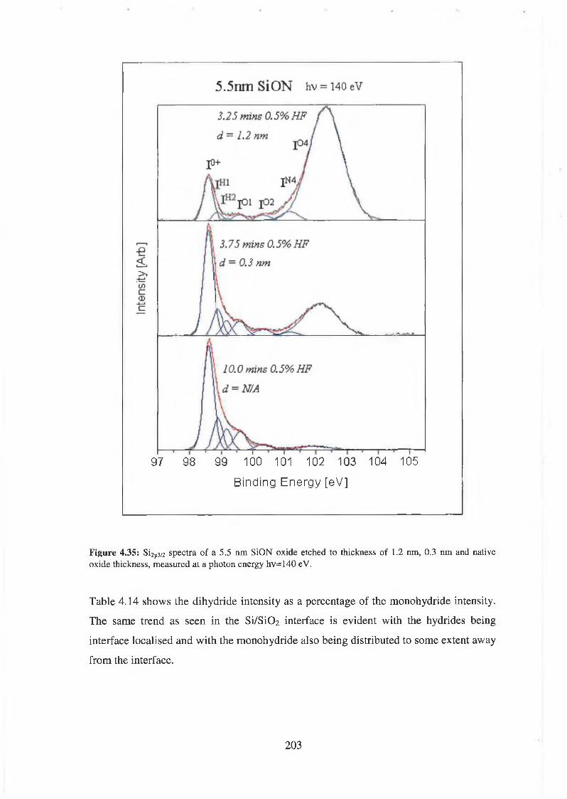
97 98 99 100 101 102 103 104 105
Bind ing E n e rg y [eV]
F igure 4.35: Si2p3/2 spectra of a 5.5 nm SiON oxide etched to thickness of 1.2 nm, 0.3 nm and native oxide thickness, measured at a photon energy hv=140 eV.
Table 4.14 shows the dihydride intensity as a percentage of the monohydride intensity.
The same trend as seen in the Si/Si02 interface is evident with the hydrides being
interface localised and with the monohydride also being distributed to some extent away
from the interface.
203
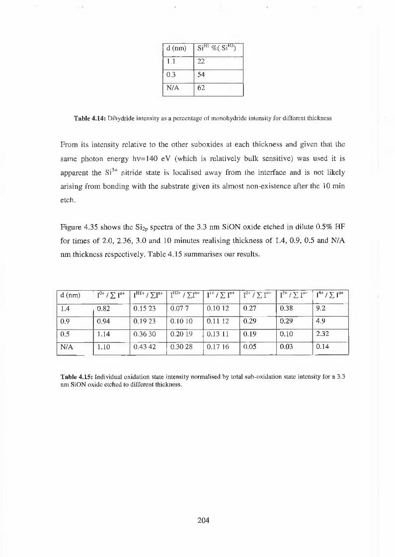
d (nm) SiH1 %( SiH2)
1.1 22
0.3 54
N/A 62
Table 4.14: Dihydride intensity as a percentage of monohydride intensity for different thickness
From its intensity relative to the other suboxides at each thickness and given that the
same photon energy hv=140 eV (which is relatively bulk sensitive) was used it is
apparent the Si3+ nitride state is localised away from the interface and is not likely
arising from bonding with the substrate given its almost non-existence after the 10 min
etch.
Figure 4.35 shows the Si2P spectra of the 3.3 nm SiON oxide etched in dilute 0.5% HF
for times of 2.0, 2.36, 3.0 and 10 minutes realising thickness of 1.4, 0.9, 0.5 and N/A
nm thickness respectively. Table 4.15 summarises our results.
d (nm) r / z r + iH1+/ z r IH2+ j £jn+ i1+/ z r I2+ / 1 In+ i +/ i r + I4+ / 1 In+
1.4 0.82 0.15 23 0.07 7 0.10 12 0.27 0.38 9.2
0.9 0.94 0.19 23 0.10 10 0.11 12 0.29 0.29 4.9
0.5 1.14 0.36 30 0.20 19 0.13 11 0.19 0.10 2.32
N/A 1.10 0.43 42 0.30 28 0.17 16 0.05 0.03 0.14
Table 4.15: Individual oxidation state intensity normalised by total sub-oxidation state intensity for a 3.3 nm SiON oxide etched to different thickness.
204
3.3nm SiON hv = !40eV
Binding Energy [eV]
F igure 4.36: Si2p3/2 spectra of a 3.3 nm SiON oxide etched to thickness of 1.4 nm, 0.9 nm, 0.5 nm and native oxide thickness, measured at a photon energy hv = 140 eV.
205

d (nm ) SiHI % ( SiH2)
1.4 32
0.9 51
0.5 64
N /A 68
Table 4.16: Dihydride intensity as a percentage o f monohydride intensity for different thickness
The distribution of states for the 3.3 nm nitrided film like the 5.5 nm film again suggest
that the Si3+ nitrogen state is localised away from the interface. The growth of the
hydride signal with continued removal of the oxide confirms its localisation at the
interface. However, having undergone the same 10 min etch as the 5.5 nm SiON film,
the hydride signal is a larger percentage of the substrate. Also the amount of residue
oxide is smaller. We propose the substrate of the 3.3 nm films has been roughened to a
greater extent than the 5.5 nm film due to the longer exposure of the substrate to the
etch because it’s thinner oxide and therefore would have been removed sooner.
4.7.2 Discussion o f results
At comparable values of resolution the Si2P spectra of the SiON samples lack the same
degree of spectral structure seen in the Si02 samples as shown in figure 4.33. This is
attributed to increased bonding complexity due the presence of N and to some extent
interface disordering resulting from the nitridation incorporation process.
The interpretation of the SiON Si2p spectra is essentially the same as that of the Si02
spectra except for the traditional Si2P3+ state being associated with the interfacial Si-N
species and the increase FWHM of the Si2P4+ oxide peak. The Si2P3+ state consistently
occurred at a chemical shift of 2.58 eV from the Si2P0+ substrate peak which is the
expected value [55] for stoichiometric Si3N4.
The association of the Si2P4+ oxide increased FWHM value to the overlap between the
traditional Si0 2 Si2P4+ oxide peak and the oxide related phase of the Si2P3+ nitrogen
species is a tentative one.
206
This is because the reduced contribution of the oxide related nitrogen phase for
thickness less than 1.4 nm should result in a corresponding reduced contribution to the
Si2p4+ oxide peak, yet no such evolution in the Si2P4+ oxide peak FWHM was evident in
the SiON samples. However despite this, it is likely that the increased FWHM is in part
due to an increased distribution of the interfacial region due to the nitridation process
itself.
In terms of evolution of sub-oxidation state intensity with thickness in the near
interfacial region, both oxynitride samples show similar behaviour. It is possible that the
Si-N bonding species exist in the oxide matrix in that the SiaN4 is not due to nitrogen
being triply coordinated to silicon at the substrate surface but instead exists in the oxide
within 1.6 nm of the substrate. This assertion is supported by the reduced relative
contribution of the Si2P3+ state to the Si2P spectrum for increased etching. In order to
conclude this more conclusively the evolution of the proposed Si-N species would need
to be measured for larger thickness. However this possible approach was not pursued
because for thickness above ~ 1.5 nm the substrate can not be “seen” through the oxide
at the optimal photon energy of 130 eV and so the contribution of the Si-N species
would have to be evaluated after de-convolution from the oxide peak.
4.8 Conclusion
The gradual and predictable removal of the oxide by dilute HF etching has allowed the
as-received dielectric layers to be profiled to thickness below 2 nm where the chemical
state and intensity distribution of interfacial sub-oxidation states has been measured.
AFM analyses of the surface microughness suggest the surface is roughened
progressively with etch time. The extent of the roughening is not significant enough to
undermine the photoemission analysis as evidenced by the stability of the Si4+ oxide
peak FWHM, which would increase progressively if the surface was severely
roughened. In undertaking synchrotron based photoemission measurements we sought
to better illuminate the interfacial region in order to see if intermediate sub-oxidation
states are present and if present, determine their relative intensity.
207

As in the XPS analysis in chapter 3, our SiC>2 samples have been prototypical in that the
relative intensity and chemical shifts of the suboxides in the SiC>2 layers agree very well
with the values in the literature. This result illustrates the point that the chemical state
nature of SiCh/Si interface is “universal” for thermal oxidation because it exists below
the oxide and remains when the steady “diffusion limited oxidation growth” stops. The
relatively large value of interface sub-oxidation state density measured in this work
most likely results from post oxidation treatment of the oxide.
From the behaviour of the Nis peak binding energy position and intensity with etching
in chapter 3 the presence of two nitrogen phases, an interfacial Si3N4 like and an oxide
related shifted phase was established. Comparison of SiC>2 and the SiON Si2P core level
spectra suggest a parameter set in which a Si-N chemical state could be consistently
fitted, but due to the inability to see the N is peak could not be conclusively identified.
From the consistency in the chemical shift and from the behaviour of the relative
intensity of the proposed Si-N state we propose that it exists in a well-defined state (i.e.
Si3N4) and is distributed in the oxide matrix.
A more quantitative description of the distribution of each sub-oxidation species in the
interfacial region would be greatly facilitated by undertaking angular resolved
measurements at a fixed photon energy and treating the SiOx photoelectron signals as
arising from different layers, as in a discrete layer model. Such analysis would allow an
estimate of the thickness of the SiOx region which in our approach is not practical to
calculate given the distribution of the individual SiOx states in the SiOx region and our
lack of knowledge of values of inelastic mean free path for individual SiOx species.
However, our aim was not that of an exact value of interface thickness or interface state
density. Such absolute values are more worthwhile for comparisons of oxides grown in-
situ and without post oxidation treatment.
The usefulness of synchrotron analysis has been in affirming the localisation of the SiOx
region within 1.6 nm of the substrate, the agreement of the SiC>2 results with the
literature, the localisation for all samples of hydrides at the interface and the divergence
of the nitrated sample results from the non-nitrated sample results on the basis of the
presence of an acceptable Si-N related chemical interface state.
208

4.9 References for Chapter IV
1 D. Vanderbilt, K. Ng, Phys Rev B 59 (1999) 10132
2 A. Pasquarello, M. Hybertson. R. Car, Phys. Rev. Lett. 74 (1995)1024
3 A. Pasquarello, M. Hybertson. R. Car, Phys. Rev. Lett. 68 (1996)625
4 A. Demkov, O. Sankey, Phys. Rev. Lett. 83 (1999) 2038
5 K. Hirose, H. Nohira, T. Hattori, Phys. Rev. B 59 (1999) 5617
6 F. Grunthaner, P. Grunthaner, R. Vasquez, B. Lewis, J. Maserjian, A. Madhukar,
Phys Rev. Lett. 43 (1979) 1683
7 K. Hubner, Phys. Status. Solidi 61 (1980) 665
8 E. Martinez, F. Yndurain, Phys. Rev. B 24 (1981) 5718
9 F. Bell, L. Ley, Phys. Rev. B 37 (1998) 8383
10 F. Himpsel, F. MeFeely, A. Ibrahimi, J. Yarmoff, G. Hollinger, Phys. Rev. B 38
(1988) 6084
11 B. Holl, F. MeFeely, Appi. Phys. Lett. 65 (1994) 1097
12 F. MeFeely, K. Zhang, B. Holl, S. Lee, J. Vac. Sci. Tec. B 14 (1996) 2824
13 B. Holl, F. MeFeely, Phys. Rev. Letts. 17 (1993) 2441
14 K. Raghavachari, J. Eng, Phys. Rev. Letts. 84 (2000) 935
15 A. Pasquarello, M. Hybertson. R. Car, Phys. Rev. B 53 (1996) 10942
16 M. Weldon et al., Surf. Sci. 500 (2002) 859
17 H. Ubara, T. Imura, A. Hiraki, Sol. State Commun. 50 (1984) 673
18 M. Matsumura, H. Fukidome, J. Electrochem. Soc. 143 (1996) 2683
19 A Crossley, C. Scofield, C. Goff, A. Lake, J. Non-Cryst. Sol. 221 (1995) 187
20 Y Chabal, G. Higashi, K. Raghavachari, J Vac Sci Technol A7 (1989) 2104
21 Y. Morita, H. Tokumoto, J Vac Sci Technol A14 (1996) 854
22 G. Pietsch, U. Kohler, U. Jusko, M Henzler, Appi Phys Lett 60 (1992) 1321
209
23 G. Higashi, K. Y Chabal, W Trucks, K. Raghavachari, Appl Phys Lett 56 (1990)
656
24 Hattori et al„ J. Vac. Sci. Technol B 11 (1993) 1528
25 K. Ohishi, T. Hattori, Jpn. J. Appl. 33 (1994) L675
26 T. Hattori, Appl. Surf. Sci. 130-132 (1998) 156
27 T. Hattori, H. Nohira and K. Takahashi, Microelectronic Engineering 48 (1999) 17
28 M. Fujimura, K. Inoue, H. Nohira, T. Hattori, Appl. Surf. Sci. 162-163 (2000) 62
29 J. Sune, I. Placencia, E Farras, N. Bamiol, X, Aymerich, Phys. Status Solidi 109
(1998) 496
30 E. Irene, S. Zafar, Q. Liu, J. Vac. Sci. Technol. A 13 (1995) 47
31 A. Carim, R. Sinclair, J. Electrochem. Soc. 134 (1987) 741
32 Q. Liu, J. Wall, E. Irene, J. Vac. Sci. Technol. A 12 (1994) 2625
33 J. Poler, K. McKay. E. Irene, J. Vac. Sci. Technol. B 12 (1994) 88
34 M. Hirose, M. hiroshima, T. Yasaka, S. Miyazaki, J. Vac. Sci. Technol. A 12
(1994) 1864
35 S. Miyazaki, T. Tamura, M. Ogasawara, H. Itokawa, H. Murakami, M. Hirose,
Appl. Surf. Sci. 159-160 (2000) 75
36 G. Tallarida, F. Cazzaniga, B. Crivelli, R. Zonca, J. Non Ctystalline solids 245
(1999)210
37 D. Mitchell, K. Clark, J. Bardwell, W. Lennard, G. Massoumi, I. Mitchell, Surf.
Intf. Anal. 21 (1994) 44
38 T. Hattori, K. Hirose, N. Nohira, K. Takahashi, T. Yagi, Appl. Surf. Sci. 144-145
(1999)297
39 J. Oh, H. Yeom, Y. Hagimoto, K. Ono, N. Hirashita, A. Kakizaki, Phys. Rev. B63
(2001)205310-1
40 D. Luh, T. Miller, T. Chiang, Phys. Rev. Lett. 79 (1997) 3014
41 I. Ohdomari, H. Akztsu, Y. Yamakshi, K. Kishimoto, J. Appl. Phys. 62 (1987) 3571
42 Y. Tu, J. Tersoff, Phys. Rev. Lett. 84 (2000) 4393
210
43
44
45
46
47
48
49
50
51
52
53
54
55
56
57
58
59
60
61
62
63
R. Buczko, S. Pennycook, S. Pantelides, Phys. Rev. Lett. 84 (2000) 943
R Haight, L Feldman, J. Appl Phys., 53 (1982) 4884
V. Atluri, N. Herbots, D. Dagel, S. Bhagvat, S. Whaley, Nuclear Instruments and
Methods in Physics Research B 118 (1996) 144
K. Yamamoto, M. Hasegawa, J. Vav. Sei. Technol. B 12 (1994) 2493
R. Uhrberg, E. Landemark, Y. Chao, J. Elect. Spect. Reit. Phenom. 75 (1995) 197
M. Niwano, H. Katakura, Y. Takeda, Y. Takakuwa, M. Maki, J. Vac. Sei. Technol.
A 10 (1992) 339
S. Tay, Z. Lu, T. Miller, J. Appl. Phys. 77 (1995) 4101
S. Tay, Z. Lu, J. McCaffrey,B. Brar, L. Feldman, Appl. Phys. Lett. 71 (1997) 2764
Z. Lu, M. Graham, D. Jiang, Appl. Phys. Lett. 63 (1993) 2941
S. Tay, Z. Lu, R. Cao, P. Pianetta, Appl. Phys. Lett. 67 (1995) 2836
J. Keister, J. Rowe,J. Kolodziej, G. Lucovsky, J. Vac. Sei. Technol. A 17 (1999)
1250
V. Gritsenko, J. Xu, R. Kwok, H, Wong, J. Non crystalline solids 297 (2002) 96
G. Dufour, F. Rochet, H. Roulet, F. Sirotti, Surface Science 304 (1994) 33
J. Bischoff, F. Lutz, D. Bolmont, L. Kubier, Surface Science 251 (1991) 170
C. Peden, J. Rogers, N.Shinn, K. Kidd, K. Tsang, Phys. Rev. B 47 (1993) 15622
R. Hedge, P. Tobin, K. Reid, B. Maiti, S. Ajuria, Appl. Phys. Lett. 66 (1995) 2882
E. Garfunkel, H. Lu, P. Gusev, M. Green, Appl. Phys. Lett. 69 (1996) 2713
V. Gritsenko, J. Xu, R. Kwok, Y. Ng, I. Wilson, Phys. Rev. Lett. 35 (1998) 1293
V. Gritsenko, N. Dikovskaja, K. Mogilnikov, Thin Solid Films 51 (1978) 353
H. Philips, J. Phys. Chem. Sol. 32 (1971) 1936
K. Behrens, E. Klinkenberg, J. Finster, K. Broer, Surf. Sei. 402 (1998) 729
V. Gritsenko, J. Xu, R. Kwok, H, Wong, J. Non Crystalline Solids 297 (2002) 96
211

65 W. Scopel, M. Fantini, M. Alayo, I. Pereyra, Thin solid films (2002) Article in
Press
66 J. Shallenberger, S. Novak, D. Cole, J. Vac. Sci. Technol. A 17 (1999) 1086
67 D. Bouvet et al, J. Appi Phys. 79 (1996) 7114
212
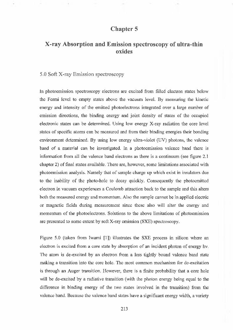
Chapter 5
X-ray Absorption and Emission spectroscopy of ultra-thin oxides
5.0 Soft X-ray Emission spectroscopy
In photoemission spectroscopy electrons are excited from filled electron states below
the Fermi level to empty states above the vacuum level. By measuring the kinetic
energy and intensity of the emitted photoelectrons integrated over a large number of
emission directions, the binding energy and joint density of states of the occupied
electronic states can be determined. Using low energy X-ray radiation the core level
states of specific atoms can be measured and from their binding energies their bonding
environment determined. By using low energy ultra-violet (UV) photons, the valence
band of a material can be investigated. In a photoemission valence band there is
information from all the valence band electrons as there is a continuum (see figure 2.1
chapter 2) of final states available. There are, however, some limitations associated with
photoemission analysis. Namely that of sample charge up which exist in insulators due
to the inability of the photo-hole to decay quickly. Consequently the photoemitted
electron in vacuum experiences a Coulomb attraction back to the sample and this alters
both the measured energy and momentum. Also the sample cannot be in applied electric
or magnetic fields during measurement since these also will alter the energy and
momentum of the photoelectrons. Solutions to the above limitations of photoemission
are presented to some extent by soft X-ray emission (SXE) spectroscopy.
Figure 5.0 (taken from Iwami [1]) illustrates the SXE process in silicon where an
electron is excited from a core state by absorption of an incident photon of energy hv.
The atom is de-excited by an electron from a less tightly bound valence band state
making a transition into the core hole. The most common mechanism for de-excitation
is through an Auger transition. However, there is a finite probability that a core hole
will be de-excited by a radiative transition (with the photon energy being equal to the
difference in binding energy of the two states involved in the transition) from the
valence band. Because the valence band states have a significant energy width, a variety
213
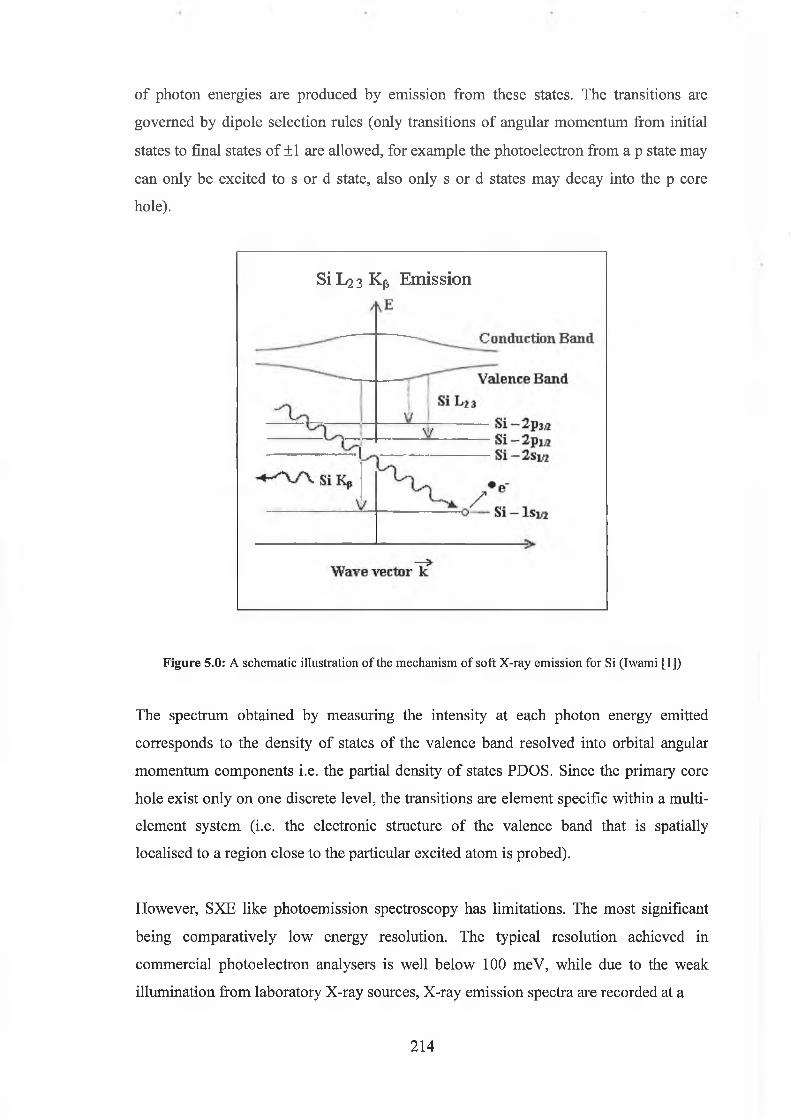
of photon energies are produced by emission from these states. The transitions are
governed by dipole selection rules (only transitions of angular momentum from initial
states to final states of ±1 are allowed, for example the photoelectron from a p state may
can only be excited to s or d state, also only s or d states may decay into the p core
hole).
Si L2 3 Kp Emission
Figure 5.0: A schematic illustration o f the mechanism o f soft X-ray emission for Si (Iwami [1])
The spectrum obtained by measuring the intensity at each photon energy emitted
corresponds to the density of states of the valence band resolved into orbital angular
momentum components i.e. the partial density of states PDOS. Since the primary core
hole exist only on one discrete level, the transitions are element specific within a multi
element system (i.e. the electronic structure of the valence band that is spatially
localised to a region close to the particular excited atom is probed).
However, SXE like photoemission spectroscopy has limitations. The most significant
being comparatively low energy resolution. The typical resolution achieved in
commercial photoelectron analysers is well below 100 meV, while due to the weak
illumination from laboratory X-ray sources, X-ray emission spectra are recorded at a
214

resolution far worse than in photoemission. Despite this, since a photon is being
detected instead of an electron, SXE can measure bulk electronic structure and the
charging of insulating samples is irrelevant. An improvement in SXE has been realised
through the combined use of grazing incidence diffraction gratings to disperse X-ray
emission and a wide area X-ray detector to measure the emission, which can be moved
under vacuum to remain at the focal point of the gratings for all energies. This allows
energy resolution comparable to that of conventional photoemission [2], The use of high
intensity monochromatic synchrotron radiation as the excitation source allows the
selective excitation of individual core levels in a multi-element system. In figure 5.1(a)
Rubensson [3] shows the total (or joint) density of states (TDOS) of silicon carbide as
measured by photoemission.
SiC Density of States
(a)
DOS a
/ \A r - f
" A -C p LPDOS J \
Si(s+d) A . ^ LPDOS f
V-16 *12 -8 -4 0
Binding Energy {«V)
Figure 5.1: Comparison o f the total density o f DOS states (a) with the C K PDOS (b) and the Si L PDOS (c) emission spectra o f cubic silicon The PDOS is reflected in the SXE spectra, whereas the global properties are monitored in PES (Rubensson [3]).
This spectrum is a complex convolution of the contribution of the p, s and d bonding
states between Si and C wavefunctions and the continuum of final states. Figure 5.1(b)
and (c) shows the local (partial) Cp and Si(s+d) DOS arising from the VB->Cis and the
VB-»Si2P transitions respectively. Here the valence band intensity is governed by the
atomic like nature of the final core hole (i.e. the valence band projection onto local
angular momentum symmetries, in accordance with dipole selection rules) and so the
local DOS can be seen in isolation.215
5.1 Soft X-ray Absoiption spectroscopy
Soft X-ray emission spectroscopy gives information about the density of occupied states
of the valence band. Soft X-ray absorption spectroscopy (SXA) gives complimentary
information to SXE concerning the empty density of states of the conduction band.
Figure 5.2 outlines the process by which absorption maybe measured.
Photii
oelectron
ï Augei 4
Ìelectron j
»
E lectron Yield
Unoccupied state s
Vacuumlevel
Occupied state s
3W-:
5int. . :
j)
hv AAV-\
V --i f >k. i
F luorescentY ieldt
(A) (B) (€)
Figure 5.2: By tuning the photon energy through an absorption edge the creation o f a core hole can be accompanied with the liberation of; (A) a photoelectron, (B) and Auger electron or in (C) with the emission o f a photon o f suitable energy.
In figure 5.2 a core hole is created with the absorption of a photon, a compensation
current filling the core hole may be recorded. In figure 5.2(B) excited electrons emitted
from the sample can be counted with a channeltron (electron yield). In figure 5.2(C) a
total count of X-ray emission due to de-exciting electrons filling core holes (fluorescent
yield). In SXA the sample is illuminated with monochromatic radiation in the 0.1 to 1
keV range. The photon energy is swept through an X-ray absorption edge and the
current through the sample is measured. By sweeping the photon energy through an
absorption edge (using synchrotron light), core electrons are excited into the conduction
band, and assuming a non-dispersive core state, the current is proportional to the PDOS
of the unoccupied conduction band. Figure 5.3 illustrates both SXE and SXA processes.
216
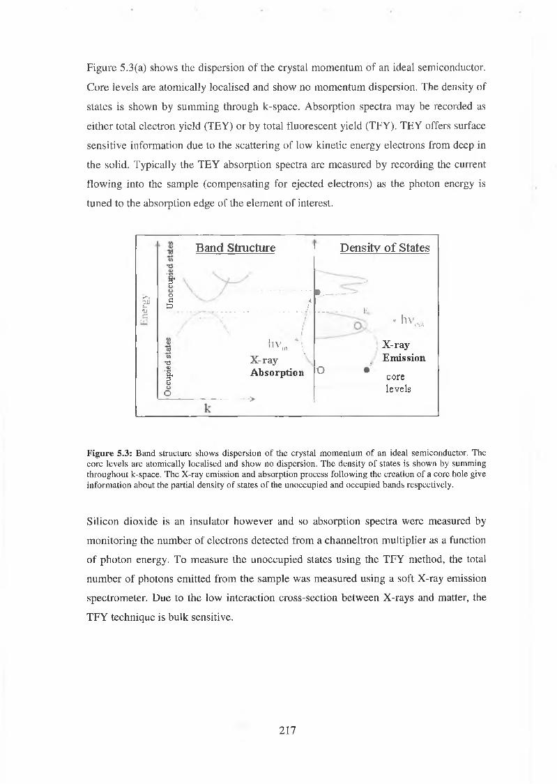
Figure 5.3(a) shows the dispersion of the crystal momentum of an ideal semiconductor.
Core levels are atomically localised and show no momentum dispersion. The density of
states is shown by summing through k-space. Absorption spectra may be recorded as
either total electron yield (TEY) or by total fluorescent yield (TFY). TEY offers surface
sensitive information due to the scattering of low kinetic energy electrons from deep in
the solid. Typically the TEY absorption spectra are measured by recording the current
flowing into the sample (compensating for ejected electrons) as the photon energy is
tuned to the absorption edge of the element of interest.
Sjs-V
3*oGtD
%
Band Structure Density o f States
................j
■ ___— —4{ F/ ----- V - - /\ j
\ ' 1 - | n -J 4 'in \ X-ray
X-ray Emission*Absorption O •
c o r e
--------------------->l e v e l s
Figure 5.3: Band structure shows dispersion of the crystal momentum of an ideal semiconductor. The core levels are atomically localised and show no dispersion. The density of states is shown by summing throughout k-space. The X-ray emission and absorption process following the creation of a core hole give information about the partial density of states of the unoccupied and occupied bands respectively.
Silicon dioxide is an insulator however and so absorption spectra were measured by
monitoring the number of electrons detected from a channeltron multiplier as a function
of photon energy. To measure the unoccupied states using the TFY method, the total
number of photons emitted from the sample was measured using a soft X-ray emission
spectrometer. Due to the low interaction cross-section between X-rays and matter, the
TFY technique is bulk sensitive.
217
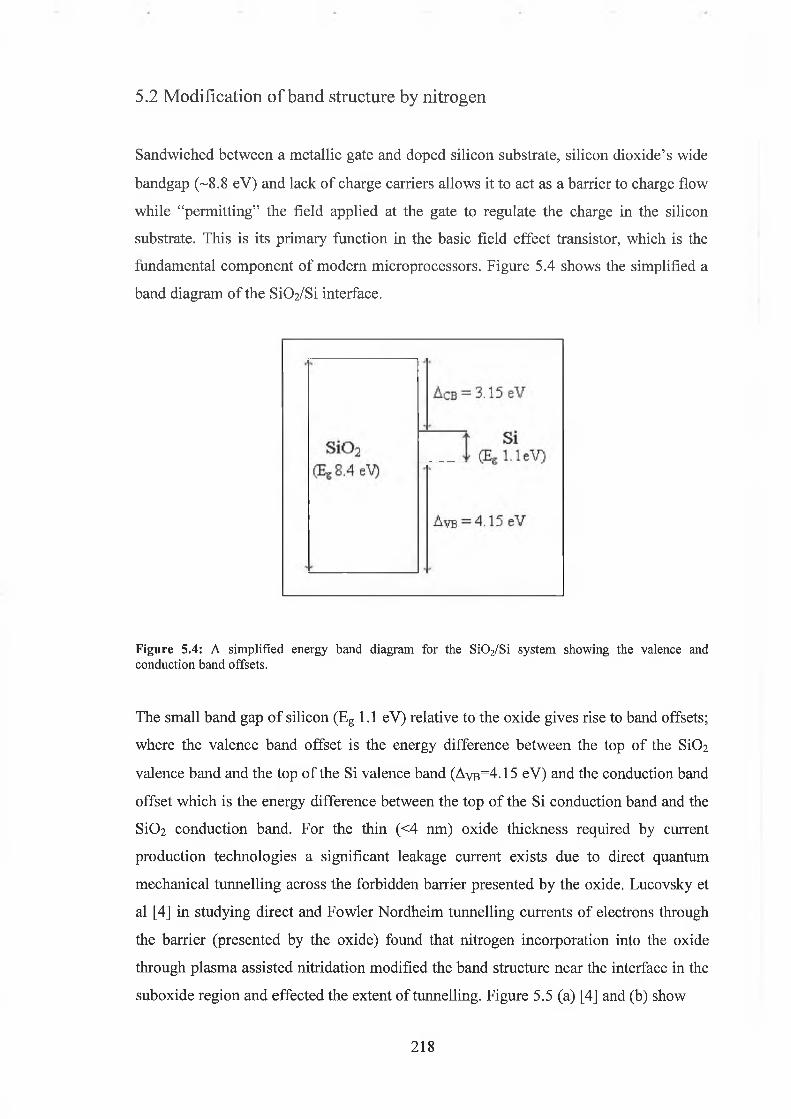
5.2 Modification of band structure by nitrogen
Sandwiched between a metallic gate and doped silicon substrate, silicon dioxide’s wide
bandgap (~8.8 eV) and lack of charge carriers allows it to act as a barrier to charge flow
while “permitting” the field applied at the gate to regulate the charge in the silicon
substrate. This is its primary function in the basic field effect transistor, which is the
fundamental component of modem microprocessors. Figure 5.4 shows the simplified a
band diagram of the SiC^/Si interface.
Figure 5.4: A simplified energy band diagram for the S i0 2/Si system showing the valence and conduction band offsets.
The small band gap of silicon (Eg 1.1 eV) relative to the oxide gives rise to band offsets;
where the valence band offset is the energy difference between the top of the SiC^
valence band and the top of the Si valence band (Avb=4.15 eV) and the conduction band
offset which is the energy difference between the top of the Si conduction band and the
S i02 conduction band. For the thin (<4 nm) oxide thickness required by current
production technologies a significant leakage current exists due to direct quantum
mechanical tunnelling across the forbidden barrier presented by the oxide. Lucovsky et
al [4] in studying direct and Fowler Nordheim tunnelling currents of electrons through
the barrier (presented by the oxide) found that nitrogen incorporation into the oxide
through plasma assisted nitridation modified the band structure near the interface in the
suboxide region and effected the extent of tunnelling. Figure 5.5 (a) [4] and (b) show
218

the proposed oxide tunnelling barriers for non-nitrided and nitrided interfacial regions
respectively. Included in the diagrams are the suboxide transition regions which define a
transition region with an average SiO composition between the Si substrate and the SiC>2
dielectric and who’s thickness were estimated to be 0.27 and 0.35 nm wide in the non-
nitrided and nitrided oxides respectively.
(a) Si02(Eg 8.8eV)
(b)
SiOx
sio2(Eg 8.8eV)
SiOx
Figure 5.5: Oxide tunnelling barriers with (a) non-nitrided and (b) nitrided suboxide interfacial regions (Lucovsky [4])
Following the results of Maserjian et al [5], Lucovsky assumed a linear variation in the
conduction band offset in the suboxide region. A difference in the conduction band
offset profiles for the nitrided and non-nitrided interfaces was confirmed from the
results of optical second harmonic generation studies. A potential step of 2.15 eV was
proposed for the nitrided interface with the remainder of the transition region being
represented by a linear variation between the top of the interface step and the SiC>2
conduction band edge. The band structure reduction in direct tunnelling in the nitrided
suboxide region relative to the non-nitrided suboxide region was estimated using an
analytical expression based on the exact solution of tunnelling through an equivalent
rectangular barrier. Lucovsky [4] observed a reduction in direct tunnelling by a factor as
much as 8+2.
219
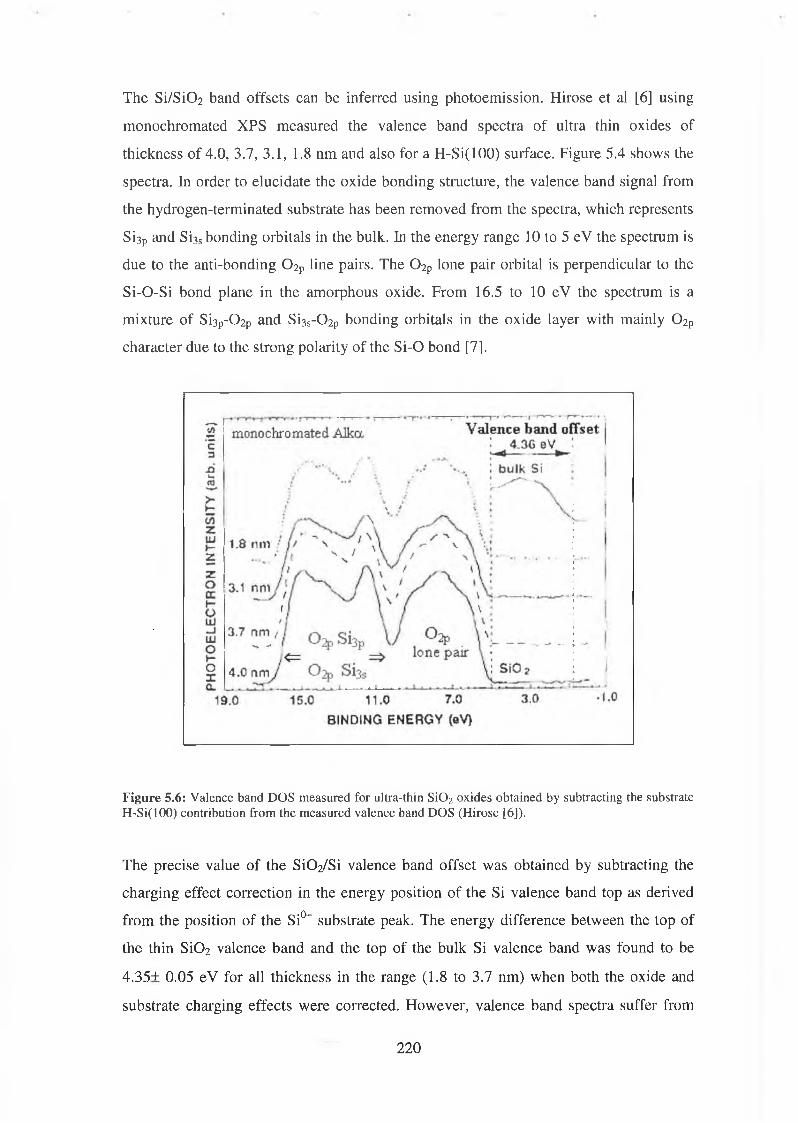
The Si/SiC>2 band offsets can be inferred using photoemission. Hirose et al [6] using
monochromated XPS measured the valence band spectra of ultra thin oxides of
thickness of 4.0, 3.7, 3.1, 1.8 nm and also for a H-Si(lOO) surface. Figure 5.4 shows the
spectra. In order to elucidate the oxide bonding structure, the valence band signal from
the hydrogen-terminated substrate has been removed from the spectra, which represents
S¡3P and Si3S bonding orbitals in the bulk. In the energy range 10 to 5 eV the spectrum is
due to the anti-bonding 0 2p line pairs. The 0 2p lone pair orbital is perpendicular to the
Si-O-Si bond plane in the amorphous oxide. From 16.5 to 10 eY the spectrum is a
mixture of Si3P-0 2p and Si3S-0 2p bonding orbitals in the oxide layer with mainly 0 2p
character due to the strong polarity of the Si-O bond [7].
Figure 5.6: Valence band DOS measured for ultra-thin S i0 2 oxides obtained by subtracting the substrate H-Si(lOO) contribution from the measured valence band DOS (Hirose [6]).
The precise value of the S i02/Si valence band offset was obtained by subtracting the
charging effect correction in the energy position of the Si valence band top as derived
from the position of the Si0+ substrate peak. The energy difference between the top of
the thin S i02 valence band and the top of the bulk Si valence band was found to be
4.35+ 0.05 eV for all thickness in the range (1.8 to 3.7 nm) when both the oxide and
substrate charging effects were corrected. However, valence band spectra suffer from
2 2 0
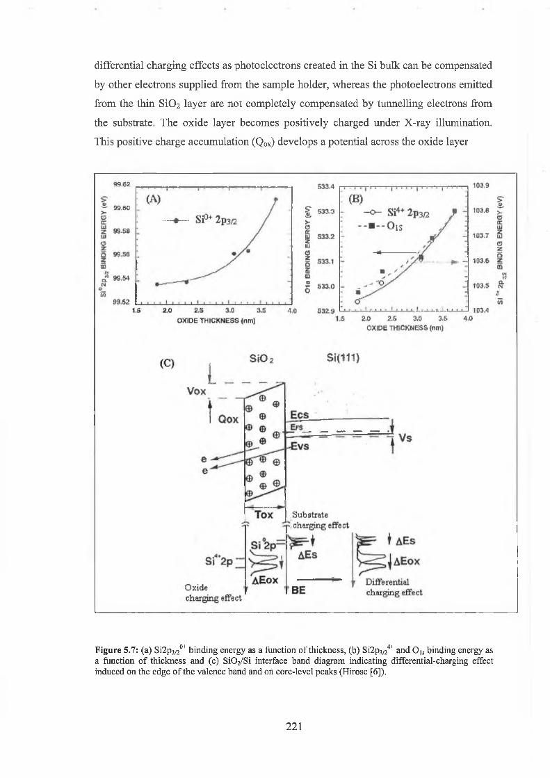
differential charging effects as photoelectrons created in the Si bulk can be compensated
by other electrons supplied from the sample holder, whereas the photoelectrons emitted
from the thin SiC>2 layer are not completely compensated by tunnelling electrons from
the substrate. The oxide layer becomes positively charged under X-ray illumination.
This positive charge accumulation (Qox) develops a potential across the oxide layer
Figure 5.7: (a) Si2p3/20+ binding energy as a function o f thickness, (b) Si2p3/24+ and Ois binding energy as a function o f thickness and (c) S i0 2/Si interface band diagram indicating differential-charging effect induced on the edge o f the valence band and on core-level peaks (Hirose [6]).
221
(Vox), modifying the energy position of the oxide valence band edge by bending the
band downward, and therefore the Si4+ and Ois core level binding energies are shifted
towards higher energies. Figure 5.7 (a) [6] shows the evolution of the Si4+ and Ois
binding energies with thickness, both peaks show similar shifts. Figure 5.7 (b) [6]
shows the shift of the substrate peak who’s shift is a fifth of the Si4+ and Ois shift. The
p-type valence band in figure 5.7 also exhibits a downward band bending (Vs) due to the
oxide charging effect but its value is smaller due to the smooth charge compensation in
the Si substrate. The difference in energy shift for Si and SiC>2 leads to the differential
charging effect. Given the difficulties of charging, the capabilities of SXE and SXA are
better suited to an examination of the band structure in order to elucidate the role of
nitrogen in the near interfacial region.
5.3 Experimental Results
SXE and SXA analysis measurements were made on the undulator beamline XIB at the
NSLS. Emission spectra were recorded using a Nordgren-type grazing incidence
spherical grating spectrometer. The spherical grating had a 5m radius of curvature with
1200 lines/mm. The nitrogen-K edge and oxygen-K edge emissions were recorded in
first order diffraction with total energy resolutions of 0.4 and 0.6 eV respectively. For
the SXA spectra the energy resolution of the monochromator was set to 0.20 eV. In
order to obtain reasonable statistical accuracy in the SXE spectra, the data was acquired
for 60-90 min per spectrum. The lower resolution in SXE arises from the need to
compensate for the lower count rate (by opening the exit slits) due to the weak process
of SXE compared to non-radiative de-excitation processes. The base pressure of the
analysis chamber was below 5x1 O'9 Torr. Absorption spectra were recorded by both the
sample drain current technique to obtain total electron yield (TEY) and by measuring
the total fluorescence yield (TFY). A 5.5 nm SiON film was thinned to a thickness of
approximately 1.7 nm (determined by XPS) by etching it in dilute 0.5% HF for 2.5 mins
followed by a rinse in deionised water before insertion into the vacuum system.
Figure 5.8(a) shows the oxygen K« SXE and SXA spectra taken from an etched SiON
and a SiC>2 sample. The SXE spectrum reflects transitions of 02P electrons from the
valence band to holes created on the Ois level, and thus measures the 0 2 P valence band
222
partial density of states. The excitation energy used to create the Ois core hole was 562
eV in both cases. The SXA spectrum was simultaneously measured by two methods
mentioned above TEY and TFY. SXE spectroscopy can be used as a probe of bulk
density of states [8,9], and also as a probe of the electronic structure of buried interfaces
[10,11]. Similar results are expected from both methods for the nitrated and non-nitrided
samples as the oxygen signal from the 1.7 nm oxide thickness is within the sampling
depth of the total electron yield method. Because the SXE and SXA spectra were
acquired separately, a calibration procedure was used to reference the SXE energy scale
to the SXA scale in order to determine the energy gap between the C>2p PDOS which
contribute to the SiON valence and conduction bands.
TFY: S i0 2 TFY: SiON TEY: SiON
SiONSi02
<- 8.8 eV->515 520 525 530 535 540 545 550
Energy (eV)
532 536 540
Energy (eV)
OK^SXA
F igure 5.8: (a) O K edge SXE and SXA spectra from both the SiON sample (line with squares) and the S i0 2 sample (solid line). The SXE spectra were obtained with an excitation energy of 562 eV. (b) The O K edge SXA spectra of SiON obtained in both TEY and TFY mode are compared with that of S i0 2 obtained in TFY mode. The SiON TFY (shown in black) spectrum shows a step extending from the conduction band edge by 3eV not observed in the S i0 2 spectrum.
223
This was performed by detecting the elastically scattered incident photons for both
absorption and emission spectra, which are then effectively referenced to the energy
calibration of the beamline monochromator. The value measured for the bandgap from
the Ou PDOS was 8.8 eV, which closely approximates to the bulk SiC>2 bandgap [12].
For comparison the O Ka SXA and SXE spectra of SiC>2 are included in figure 5.8(a)
and are essentially the same as that obtained from the SiON film though the Û2P. PDOS
from the SiON film shows minor differences. Figure 5.8(b) shows a clear difference
when comparing the measured SXA spectrum obtained in the TFY mode (bulk
sensitive) between the S i02 and the SiON spectra with a visible step extending
downwards from the conduction band edge by about 3 eV.
Figure 5.9: N K edge SXE and SXA spectra from the SiON sample (top). The SXA spectrum was obtained with an excitation energy of 440eV. The N K edge SXE spectrum obtained from a-S i3N4 is shown (middle) as well as that of molecular N 2 (bottom).
A similar reduction of 3 eY in the conduction band onset has been observed by Muller
et al [13] through EELS measurements on interfacial oxides at the interface between Si
and S i02 and has been attributed to induced gap states predicted to be present at all
Si/Si02 interfaces. In figure 5.8(b) however, the step is not observed in Si02 but is in
the TFY obtained from the oxynitride sample and must therefore be a feature of the
224
Si/SiON interface. Figure 5.9 shows the Nis SXA and SXE spectra measured from the
same SiON sample, from a a-Si3N 4 and from molecular N2.
The SXA and SXE spectra, which are measures of the unoccupied and occupied N2P
PDOS respectively, indicate that the energy bandgap is of the order of 5 eV. This
bandgap approximates that of Si3N4. The excitation energy used to create the N js core
hole was 435 eV. Finally figure 5.10 shows two separate N is SXE spectra, one taken at
threshold at an excitation energy of 402 eV the second was obtained at an excitation
energy of 435 eV. A shift was observed between the leading edge of the emission
spectra, but also a change in the energy spacing of the peaks between the two spectra
can be observed.
Energy (eV)
F igure 5.10: N K edge SXE spectrum o f SiON sample obtained above threshold (solid line - top) and at threshold (dashed line - bottom). The lines represent 3pt moving averages o f the data to guide the eye.
225
5.4 Discussion of results
A number of band structure calculations are available for SÍ3N4 and also for SÍ2N2O
whereas at present few calculations exist for silicon oxynitride systems with more dilute
nitrogen concentrations such as those found in industrial device grade material [14,16].
Ance et al [17] have undertaken theoretical calculations for a unique disordered SiOxNy
phase with a random distribution of Si-0 and Si-N bonds the probability of which is
determined by the relative oxygen and nitrogen concentration. Their calculations have
indicated that for low nitrogen concentrations, the width of the N2p lone-pairs which
form the top of the valence band decrease rapidly while the bottom of the conduction
band is a combination of SÍ3P, N2P and 0 2 P antibonding states.
Their results show that the optical absorption edge changes from approximately 5.5 eV
for the nitrogen rich material (SÍ3N4 like) to approximately 9 eV for SÍO2. Also the
shape of the optical absorption has a step like feature similar to that in our TFY SXA
spectrum in figure 5.9 where the step extends from the conduction band edge some 2-3
eY for 0/(0+N) ratios in the range of 0.8-0.98, where our bulk 0/(0+N) ratio was
approximately 0.95.
Wiech et al [18] and Gians et al [19] have undertaken SXE spectroscopy on 01-SÍ3N4 and
molecular N2 respectively. It is possible to directly compare our results for the N2P SXE
from the SiON with these reference spectra (see figure 5.9). A difference in the position
of the valence band maximum of ~0.4 eV between our SiON spectrum and the OC-SÍ3N4
spectrum taking into account instrumental broadening was found. The main peak of
emission is coincident with that of SÍ3N4 and that of molecular N2 . The N2P valence
bandwidth was comparable to that of OC-SÍ3N4 and was ~10 eV. The strongest peaks in
the emission had an energy difference of 2.3 eV for SiON 3.09 eV for SÍ3N4 and 1.4 eV
for N2. In analysing the SXE spectra of (X-SÍ3N4 Wiech [18] identified the origin of the
three peaks denoted A, B and C in figure 5.9 by comparison to calculations of the partial
density of states. He determined peak A to be a mixture of SÍ3¡¡, SÍ3d and N2p
components, peak B to be a mixture of SÍ3P and N2p and peak C to be mainly due to SÍ3S.
Band structure calculations by Xu et al [16] of the SÍ2N2O result in a sharper partial
density of states closer to the valence band maximum in broad agreement with that
226
observed in this study. Figure 5.10 shows the N2p SXE spectra recorded with a photon
excitation energy close to the Nis absorption threshold (403 eV) and far above the
threshold at 435 eV. The latter spectrum was the same as presented in figure 5.7 and
reflects the N2p PDOS. Clear differences between the positions of the peaks in the
emission spectra can be seen for the above threshold spectrum and the threshold
spectrum in figure 5.8. The peak designated A has shifted by -0.35 eV in the threshold
spectrum relative to the above threshold spectrum, peak B has shifted by -0.15 eV and
peak C has not shifted. Such a change in profile on resonant excitation is an indication
of the probing of different N sites in the SiON layer, the existence of which have
previously been indicated by photoemission as being N-Si3 and N-Si2 bonding
environments in a dilute nitrogen SiOxNy sample. Our photoemission results indicated
that nitrogen exists near the interface and is bonded to silicon. It is in this region that the
narrowing of the bandgap would contribute to the reducing of the band offsets between
Si and S i02. This is agreement with the results reported by Lucovsky et al [4] for
nitrogen having an influence on the oxide bandgap in the interfacial region of nitrided
oxides.
5.5 Conclusion
The experimental findings to date suggest that the distribution of nitrogen in ultra thin
SiON films is, both process dependent and interface dependent. The picture, which
emerges from these studies, is that the ammonia based nitridation of the Si02 layer of
the S i02 dielectric layer results in the build up of nitrogen at the Si-Si02 interface and in
the near surface region of the oxide. The photoemission data is consistent with the
nitrogen bonding in a N(-Si3) bonding environment at the interface. The SXE and SXA
data indicate that the contribution of the N2p occupied and unoccupied states to the
conduction and valence bands respectively, generate an interfacial bandgap of 5 eV
which would significantly modify the band offset between Si and it’s oxide.
227

5 . 6 R e f e r e n c e s f o r C h a p t e r V
1 M. Iwami, Appl. Surf. Sci. 113/114 (1997) 377
2 K. Smith, submitted for publication
3 J. Rubensson, J. Electron Spectrosc. Relat. Phenom 92 (1998) 189
4 G. Lucovsky, J. Keister, J. Rowe, Hiro Nimmi, Appl. Surf. Sci. 166 (2000) 485
J. Maserjian, N. Zamani, J. Appl. Phys. 53 (1982) 559
M. Hirose, J Alay, T. Yoshida, The Physics and Chemistry of Si02 and the Si-Si02
interface -3 H. Massoud Proc. Vol. 96-1 p. 485
7 F. Bell, L. Ley, Phys. Rev. B 37 (1988) 8383
8 C. Stagarescu, L. Duda, K. Smith, et al, Phys Rev B54 (1996) R17335
9 K. Smith, L. Duda, et al, J. Vac. Sci. Tech. B 16 (1998) 2250
10 P. Nilsson, J. Kanski, J. Thordson, et al, Phys. Rev. B52 (1995) R8643
11 P. Nilsson, S. Mankefors, E. Lundgren, J. of Alloys and Compounds 286 (1999) 31
12 S. Sze, Physics of Semiconductor Devices. Wiley 1981 2nd Ed.
13 D. Muller, T. Sorsch, S. Moccio, F. Baumann, K. Evans, G. Timp, Nature 399
(1999)758
14 A. Ivanovskii, N. Medvedeva, O. Kontsevoi, Physica Status Solidi B 221(2000) 647
15 G. Pacchioni, D. Erbetta, Phys Rev B 60 (1999) 12617
16 Y. Xu, W. Ching, Phys. Rev. B 51 (1995) 17379
17 C. Ance, F. de Chelle, J. Ferraton, Appl. Phys. Lett. 60 (1992) 1399
18 G. Wiech, A. Simunek, Phys. Rev. B 49, (1994) 5398
19 P. Gians, P. Skytt, K. Gunnelin, J. Electron Spectrosc. Relat. Phenom. 82 (1996) 193
2 2 8
Chapter 6
C ore-level photoemission studies o f the sulphur terminated Si(100) and Ge(100) surfaces
6.0 Introduction
The reduced size of semiconductor devices resulting from the drive towards increased
device density in modern IC technology has inevitably resulted in the increased role of
the surface and it’s properties in shaping the electronic properties of these devices. The
surface structure of the (100) and (111) surfaces of germanium and silicon represent
prototype systems for the investigation of surface bonding involving double and single
dangling bonds, respectively. Several studies have investigated the possibility of
terminating the (100) surfaces of these semiconductors by an adsorbed monolayer of the
group VI element, sulphur. This structure has the potential to eliminate all surface
dangling bonds, producing an ideal bulk ( lx l) termination of very low chemical
reactivity suitable for subsequent hetroepitaxial growth. An ideal sulphur monolayer-
terminated surface would also be of significant technological importance if it were a
perfect surface termination. This is especially true if it proved to be atomically abrupt, a
level of perfection that cannot be achieved with the Si/Si02 interface. It would be an
ideal surface for the subsequent deposition of high dielectric constant materials in
nanoscale transistor fabrication as the surface dangling bond density would be
extremely low.
6.1 Si(100) bulk and surface structure
Silicon is a group IV element. It crystallises in the diamond structure where it is co
ordinated tetrahedraly to four other silicon atoms through bond angles of 109° 28 (see
figure 6.0) [1]. Unlike its oxide there is long range order in the bulk crystal structure due
to the absence of the flexible Si-O-Si inter tetrahedral bridge bond.
229
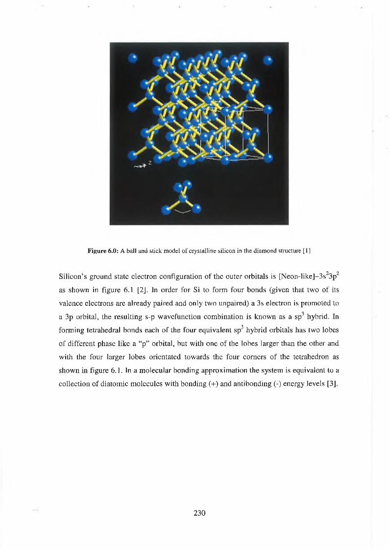
r-***
V
F igure 6.0: A ball and stick model of crystalline silicon in the diamond structure [1]
2 2Silicon’s ground state electron configuration of the outer orbitals is [Neon-like]-3s 3p
as shown in figure 6.1 [2]. In order for Si to form four bonds (given that two of its
valence electrons are already paired and only two unpaired) a 3s electron is promoted to
a 3p orbital, the resulting s-p wavefunction combination is known as a sp3 hybrid. Ina
forming tetrahedral bonds each of the four equivalent sp hybrid orbitals has two lobes
of different phase like a “p” orbital, but with one of the lobes larger than the other and
with the four larger lobes orientated towards the four corners of the tetrahedron as
shown in figure 6.1. In a molecular bonding approximation the system is equivalent to a
collection of diatomic molecules with bonding (+) and antibonding (-) energy levels [3],
230
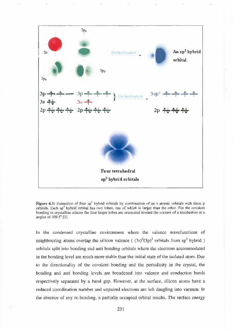
3pï
m3 s W ÊÈ m Aii sp3 hybrid
» •I " 13px
orbital
3 p ^ ^ ---------------------------------------u n , . , , , ™ 3 s p 3 ^ ^ - ^ ^ -
3s 4 ^. 3s - f* *
2 p ^ N r4 ^ " N r 2 p 4 ^ 4 ^ 4 ^ 2p 4 ^ 4 ^
♦
Four tetrahedral
sp3 hybrid orbitals
Figure 6.1: Formation of four sp3 hybrid orbitals by combination of an s atomic orbitals with three p orbitals. Each sp3 hybrid orbital has two lobes, one of which is larger than the other. For the covalent bonding in crystalline silicon the four larger lobes are orientated toward the corners of a tetrahedron at a angles of 109.5° [2],
In the condensed crystalline environment where the valence wavefunctions of2 2 * 3neighbouring atoms overlap the silicon valence ( (3s) (3p) orbitals from sp hybrid )
orbitals split into bonding and anti bonding orbitals where the electrons accommodated
in the bonding level are much more stable than the initial state of the isolated atom. Due
to the directionality of the covalent bonding and the periodicity in the crystal, the
bonding and anti bonding levels are broadened into valence and conduction bands
respectively separated by a band gap. However, at the surface, silicon atoms have a
reduced coordination number and unpaired electrons are left dangling into vacuum. In
the absence of any re-bonding, a partially occupied orbital results. The surface energy
231

and symmetry can be reduced by a rearrangement of the outer surface atoms, which
causes the occupied orbital to split into a (higher) unoccupied (antibonding) orbital and
a (lower) doubly occupied (bonding) orbital. The trade off between the gain in
electronic energy versus the energetic cost of the atomic arrangement decides whether
such a surface reconstruction occurs. Duke [4] has outlined three general principles,
which help decide whether or not a surface reconstructs:
• The first is the tendency for atoms on the surface of tetrahedraly coordinated
semiconductors to “reconstruct” or rearrange so as to either “saturate” (satisfy
the valence) the surface atom’s “dangling” (broken) tetrahedral bonds that would
occur if the surface were to retain its truncated bulk geometry, or to convert
them into non bonding electronic states.
• The second principle of semiconductor surface reconstruction is that in many
cases, surfaces can lower their energies by atomic reconstruction that opens an
energy gap between the highest occupied and lowest unoccupied surface states,
giving rise to an insulating or semiconducting surface as opposed to a metallic
surface.
• The third principle of surface reconstruction helps to distinguish between
activated and activationless surface reconstructions. Activated surface
reconstructions have energetic barriers that must be overcome in order to obtain
them, whereas activationless surface reconstruction have little or no barrier to
obtain them. The surface reconstruction observed will be the lowest structure
kinetically accessible under the preparation conditions.
Figure 6.2 (a) [5] shows the truncated Si(100) surface. There are two dangling bonds sp3
hybrid orbitals per surface atom, which appear like “rabbit ears” on the outer most
surface atom (shown in white). This surface geometry is unstable and the surface
reconstructs in such a way as to saturate surface dangling bonds (as predicted by the
first principle above), and to produce an insulating surface (as predicted by the second
principle above) while minimising the elastic energy associated with the distortion of
the tetrahedral bond angles away from their bulk values.
232

DBdown
DB„
F igure 6.2: a),b),c) and d) (Top panel [5]) shows the ball and stick models o f bonding between unterminated surface bonds for the unreconstructed and reconstructed Si(100) surface [5]. a),b),c) and d) (Bottom panel) show the energy level diagrams with the bonding and anti-bonding states formed associated with surface geometries shown in the ball and stick models (top panel [35]).
Surface dimers (figure 6.2 (b)) are formed when the atoms of the truncated bulk re-bond
pairwise to reduce the number of surface dangling bonds per atom to one for the
reconstructed surface from two for the unreconstructed surface. In the dimer, sigma (ct)
bonding results with pairs of sp3 orbitals directed along the bond. A weaker form of
bonding called pi ( 71) bonding can occur, which is purely between p orbitals whose axis
is perpendicular to the bond. Dimer formation lifts the four-fold degeneracy with
adjacent sigma pairing resulting in bonding (a) and anti bonding (a*) sigma states. Pi
bonding between the remaining two dangling bonds (figure 6.2 (c)) splits the remaining
degeneracy into bonding ( 71) and anti bonding ( 71*) pi states. These states spread into the
nearly one-dimensional surface bands along rows formed by dimer pairs resulting in a
metallic surface. However for many years there has been disagreement among
experimentalists about the nature of the surface reconstruction of Si(100). The
symmetric dimer model is supported by the observation of a double domain (2x1)
LEED [6] pattern from clean surfaces with monatomic steps. Also, room temperature
STM images reveal symmetric dimers [7,8]. Angular resolved photoemission studies,
233
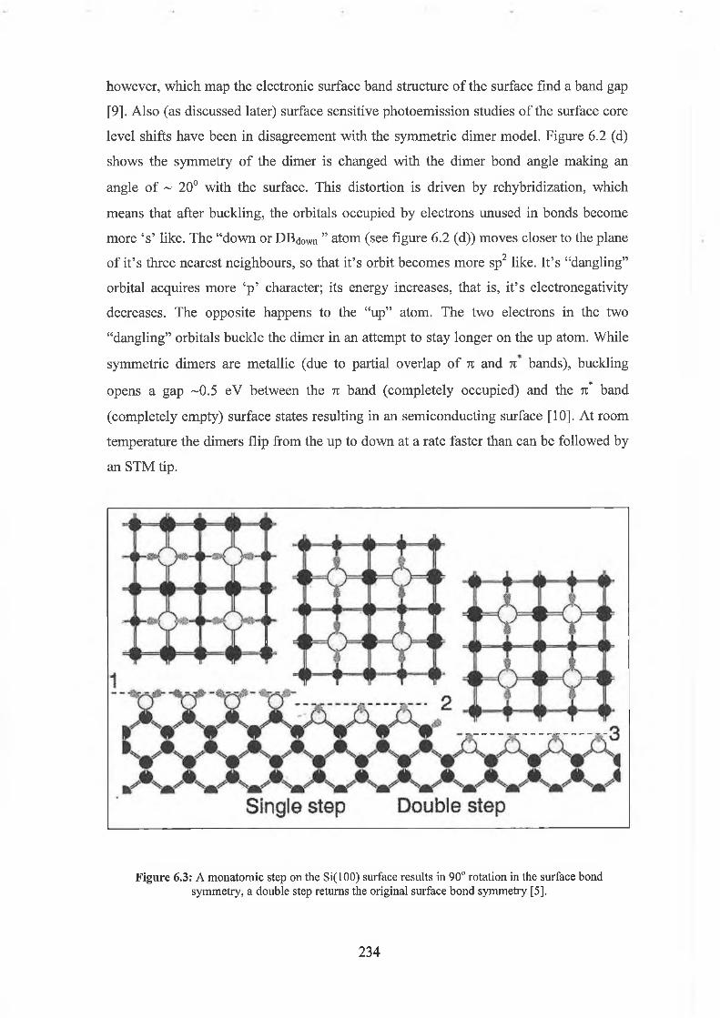
however, which map the electronic surface band structure of the surface find a band gap
[9]. Also (as discussed later) surface sensitive photoemission studies of the surface core
level shifts have been in disagreement with the symmetric dimer model. Figure 6.2 (d)
shows the symmetry of the dimer is changed with the dimer bond angle making an
angle of ~ 20° with the surface. This distortion is driven by rehybridization, which
means that after buckling, the orbitals occupied by electrons unused in bonds become
more ‘s’ like. The “down or DBdown ” atom (see figure 6.2 (d)) moves closer to the plane• • • 2 * • of it’s three nearest neighbours, so that it’s orbit becomes more sp like. It’s “dangling”
orbital acquires more ‘p ’ character; its energy increases, that is, it’s electronegativity
decreases. The opposite happens to the “up” atom. The two electrons in the two
“dangling” orbitals buckle the dimer in an attempt to stay longer on the up atom. While
symmetric dimers are metallic (due to partial overlap of tt and n bands), buckling
opens a gap ~0.5 eV between the n band (completely occupied) and the n* band
(completely empty) surface states resulting in an semiconducting surface [10]. At room
temperature the dimers flip from the up to down at a rate faster than can be followed by
an STM tip.
Figure 6.3: A monatomic step on the Si(100) surface results in 90° rotation in the surface bond symmetry, a double step returns the original surface bond symmetry [5].
234

Figure 6.3 [5] shows a top and side view of the truncated Si(100) surface with a single
and double step. Removing a single monolayer of atoms (a single step) uncovers a 90°
rotation in the surface orientation, which after a double step is returned to the original.
Thus for the reconstructed surface dimer rows run perpendicular to each other on atomic
planes separated by single steps. Figure 6.4(a) [11] shows a room temperature (0.2(im x
0.2|_im) STM image of a clean Si(100) which has single atomic steeps.
A
Figure 6.4: UHV STM images of atomically clean Si(100). a) A large area 0.2 x 0.2 (im scan showing monatomic steps, a) A high-resolution 10 x 10 nm scan across a monatomic step. The mutually perpendicular directions o f the (1x2) and (2x1) dimer domains on the surfaces is visible in the images an is highlighted in the insets [11].
235
Figure 6.4 (b) shows a magnified (10 nm x 10 nm) view of the boundary of a
monatomic step. The different orientations of the dimer rows are visible in the image
and are illustrated in the insets.
6.2 LEED Structure
In order to appreciate some of the above results it is useful to consider the surface
periodicity. The periodicity of bulk solids can be investigated with X-rays. A diffracted
beam of X-rays will emerge from a bulk crystal whenever constructive interference
occurs between successive planes of atoms in the real space lattice. The diffraction
condition is more easily determined in reciprocal space where within the Ewald sphere
the change in momentum (only direction is changed) on being elastically scattered is
equal to a reciprocal lattice vector. The position of the diffracted beams offers
information about the crystal lattice size and symmetry. Analysis of the intensity gives
information about the arrangement of atoms within the lattice (the crystal basis).
We cannot use X-ray beams in order to probe the periodicity of the surface however
because of the small scattering interaction between X-rays and the charge distribution
on atoms which results predominately in bulk information which would dominate the
smaller surface signal. Low energy electrons however have a very strong interaction
with matter and have a short mean free path (for E < 150 eV). Also, the wavelength of
such electrons is slightly smaller (a few angstroms) than typically interatomic spacing
and therefore suitable for diffraction experiments. In a LEED experiment a beam of
monochromatic low energy electrons is incident on the clean surface. The electrons are
backscattered from the sample surface onto a system of grids. Only the elastically
scattered electrons form the LEED pattern and are accelerated towards a fluorescent
screen where a pattern of bright spots is seen. The inelastically scattered electrons are
rejected by the negative potential of the other two grids.
Figure 6.5 (a) shows the ball and stick model of the truncated Si(100) surface, the green
grid show the real space representation and shown in black, the resulting (reciprocal
space) LEED pattern. Figs 6.5 (b) and (c) show the (1x2) and (2x1) reconstructions
respectively and their corresponding LEED patterns. However as mentioned above the
236
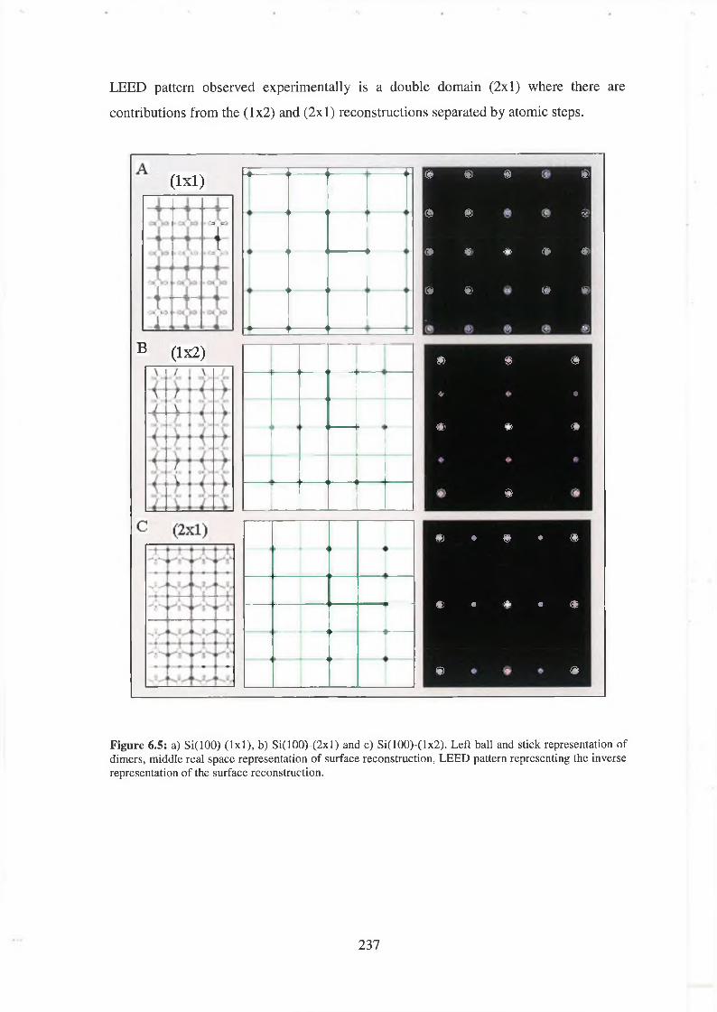
LEED pattern observed experimentally is a double domain (2x1) where there are
contributions from the (1x2) and (2x1) reconstructions separated by atomic steps.
(1x1) ♦ ♦
1
"
♦
1
1
' 1
B (1X2)
«I ® 0 *
<$> ® Çf)
® « * * «
® « * ©
<>
* « «
+ •
$ * <*
I *
* « « * m
*■ e * « <#
« «
Figure 6.5: a) Si(100) ( lx l) , b) Si(100)-(2xl) and c) Si(100)-(lx2). Left ball and stick representation of dimers, middle real space representation of surface reconstruction, LEED pattern representing the inverse representation of the surface reconstruction.
237
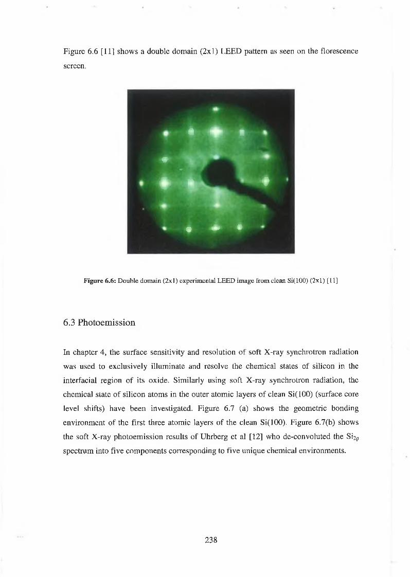
Figure 6.6 [11] shows a double domain (2x1) LEED pattern as seen on the florescence
screen.
♦ ♦ •
*
♦ ♦ 4
• - •
F igure 6.6: Double domain (2x1) experimental LEED image from clean Si(100) (2x1) [ 11]
6.3 Photoemission
In chapter 4, the surface sensitivity and resolution of soft X-ray synchrotron radiation
was used to exclusively illuminate and resolve the chemical states of silicon in the
interfacial region of its oxide. Similarly using soft X-ray synchrotron radiation, the
chemical state of silicon atoms in the outer atomic layers of clean Si(100) (surface core
level shifts) have been investigated. Figure 6.7 (a) shows the geometric bonding
environment of the first three atomic layers of the clean Si(100). Figure 6.7(b) shows
the soft X-ray photoemission results of Uhrberg et al [12] who de-convoluted the Si2P
spectrum into five components corresponding to five unique chemical environments.
238
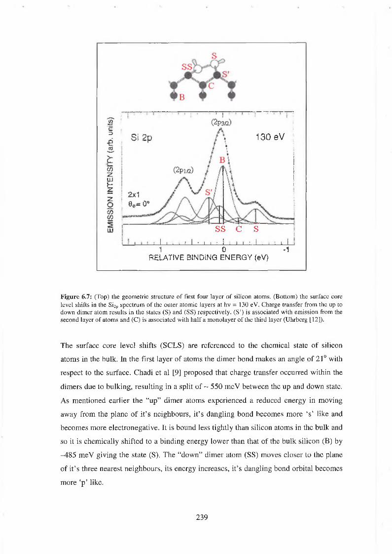
ss c st I I ; i I I • t I : I ■ I I ; ! . . i 1 i ■
1 0 '1 RELATIVE BINDING ENERGY (eV)
130 eV
Figure 6.7: (Top) the geometric structure of first four layer of silicon atoms. (Bottom) the surface core level shifts in the Si2p spectrum of the outer atomic layers at hv = 130 eV. Charge transfer from the up to down dimer atom results in the states (S) and (SS) respectively. (S’) is associated with emission from the second layer of atoms and (C) is associated with half a monolayer of the third layer (Uhrberg [12]).
The surface core level shifts (SCLS) are referenced to the chemical state of silicon
atoms in the bulk. In the first layer of atoms the dimer bond makes an angle of 21° with
respect to the surface. Chadi et al [9] proposed that charge transfer occurred within the
dimers due to bulking, resulting in a split of ~ 550 meV between the up and down state.
As mentioned earlier the “up” dimer atoms experienced a reduced energy in moving
away from the plane of it’s neighbours, it’s dangling bond becomes more ‘s’ like and
becomes more electronegative. It is bound less tightly than silicon atoms in the bulk and
so it is chemically shifted to a binding energy lower than that of the bulk silicon (B) by
—485 meV giving the state (S). The “down” dimer atom (SS) moves closer to the plane
of it’s three nearest neighbours, its energy increases, it’s dangling bond orbital becomes
more ‘p ’ like.
239

The electronegativity of this down atom decreases and the peak is difficult to assign as
it almost “sits” directly underneath the bulk core level peak shifted by only 62 meV.
The state (S’) has a shift of 220 meV and is associated with photoemission from atoms
in the second layer. A possible interpretation for the component (C) shifted by -205
meV suggested by Uhrberg [12] was that of emission from half the third layer.
6.4 Group IV Semiconductor Surface passivation
From earlier considerations it is apparent that the surface of clean Si(100) reconstructs
from the bulk ( lx l) periodicity to a (2x1) as described by the asymmetric dimer model.
In doing so the dangling bond density per surface atom is reduced from two to one.
However the resultant surface still has unteriminated bonds and is thus chemically
reactive.
Adsorption of adatoms can change the surface reconstruction in many ways by
formation of new bonds. It has been shown (Bringans [13], Olmstead [14] and Uhrberg
et al [15]) that unreconstructed S i( ll l) and G e (lll) surfaces can be obtained if the
surface layer of Si or Ge is replaced by As atoms. This occurs because As atoms have
one extra valence electron compared to Si or Ge atoms, and thus the occupied surface
orbitals for the clean surface are replaced by a fully occupied or lone pair orbital. A
monlayer of arsenic atoms has been shown by Uhrberg et al [16] to provide a passivated
coverage on the Si(100) surface. Here the Si-Si dimers of the clean surface
reconstruction are broken and the As-As dimer are added on top. The extra valence
electron on each As atom again leads to fully co-ordinated atoms.
Adsorption of sulphur and selenium shows particular interesting structural properties in
that a monolayer of these adatoms could completely remove the surface reconstruction.
However, initially this possibility was only a theoretical one. For S on Ge(100) Weser et
al [17] reported the preparation of a well ordered Ge(100)-(lxl) configuration. Using
core level spectroscopy, photoemission measurements and total energy minimisation
calculations Weser et al [17] identified a bond geometry with S atoms residing in bridge
positions above Ge atoms of the topmost layer. For S or Se monolayers on Si(100) that
particular configuration has not been observed until recently. Also, there exists
240
disagreement about the ideal termination of Si(100) by S adsorption which shall be
discuss shortly.
It is useful when considering a likely elemental candidate (S or Se) to passivate the
surface dangling bonds and restore the surface periodicity to the bulk value to examine
the implications of the valency and atomic radius of the potential adatom. Kaxiras [18]
has outlined a set of empirical criteria for evaluating surface-adsorbate combinations
that can lead to semiconductor surface restoration.
The first criterion is: with respect to a given substrate, the adsórbate atom must be either
of a lower valence, such that the occupancy of broken bonds is eliminated, or of a
higher valence, such that broken bonds are reduced to fully occupied nonbonding states.
For silicon (valence 4), a bulk terminated S i( l l l) plane consists of threefold bonded
atoms with one broken covalent bond, containing a single unpaired electron on each
surface atom. Replacing the surface Si atoms by adsorbates of valence either 3, which
would eliminate unpaired electrons, or 5, which would create a pair of non-bonding
electrons.
However, because of differences in bulk phase between the adsórbate and substrate the
first criterion alone doesn’t guarantee the resulting surface restoration is stable. For
example the bulk phase (a layered structure where every atom has three close
neighbours bonded through sp hybrids [19] ) of group V elements (e.g. P or As) is
similar to that of S i( l l l ) and leads to the restoration of S i( l l l) surface. However the
bulk phase of group III elements (eg. Al, Ga. In) is different (a metallic close packed
structure with the number of neighbours varying from 12 (Al) to 4 (In) [10]) and results
in complicated surface reconstruction without restoring the S i( l l l) bulk terminated
geometry. Thus the second criterion is that the adsórbate must exist in a bulk phase with
the same local bonding geometry as in the restored surface.
A third criterion arises from consideration of the implications of differences in atomic
radii between the adsórbate and substrate [20], The third criterion says that it is
necessary to discriminate between elements of different atomic sizes due to the
possibility of adsorbate-induced surface stress. Also the differences between bond
angles of the adsórbate in its bulk phase and in its restored surface geometry. When the
241

covalent radii of the adsórbate and substrate atoms are similar to within a few percent,
the prospects for stability increase, since the substrate-adsorbate bonds in the restored
surface will have a bond length comparable with both constituents, which tends to
reduce the stress.
A fourth criterion concerns the adverse effect of chemical reactivity on surface
restoration. It is possible that the adsórbate reacts strongly with the substrate forming
volatile molecules. The net result might be a continuous etching of the surface, rather
than the formation of a stable adsorbed layer. Alternatively it might be difficult to
deposit a suitable elemental adsórbate if its molecular compounds do not decompose on
the surface under normal adsorption conditions.
On the basis of the first criterion elements with a valence of 2 or 6 are a natural choice.
From the second criterion, group VI elements (O, S, Se, Te) are more promising« , o .
because they tend to form structures with two fold coordination and sp -bonding
hybrids as required for the restoration of Si(100). Te is eliminated by the third criterion
since it’s average bulk bond length differs from that of Si by +22%. For oxygen the Si-
O bond length is much shorter than Si-Si bonds ( so the third criterion is not satisfied )
and the Si-0 bond is energetically much stronger than Si-Si, making the formation of a
stable O overlayer on Si(100) unlikely. S and Se are likely candidates as they satisfy the
four criteria although their average bulk bond lengths differ from that of bulk Si.
However, the S-Si bond energy is larger than that of Si-Si and so Kaxiras concluded that
both chemical reactivity and induced stress would tend to inhibit the formation of an
ordered S monolayer on Si(100) where as the restoration of Si(100) by Se would be
more likely. On the basis of the above considerations the core level results for the clean
and sulphur terminated Si(100) surface are presented.
6.5 Si(100) Experimental
As in the oxynitride analysis, soft X-ray photoemission analysis was performed on
beamline U4A at the NSLS. A UHV compatible electrochemical S cell was mounted
onto the system via a 4-inch knife edge flange allowing line of sight effusion of S onto
the sample. After a 12-hour bake at 120 °C with subsequent degassing cycles a base
242
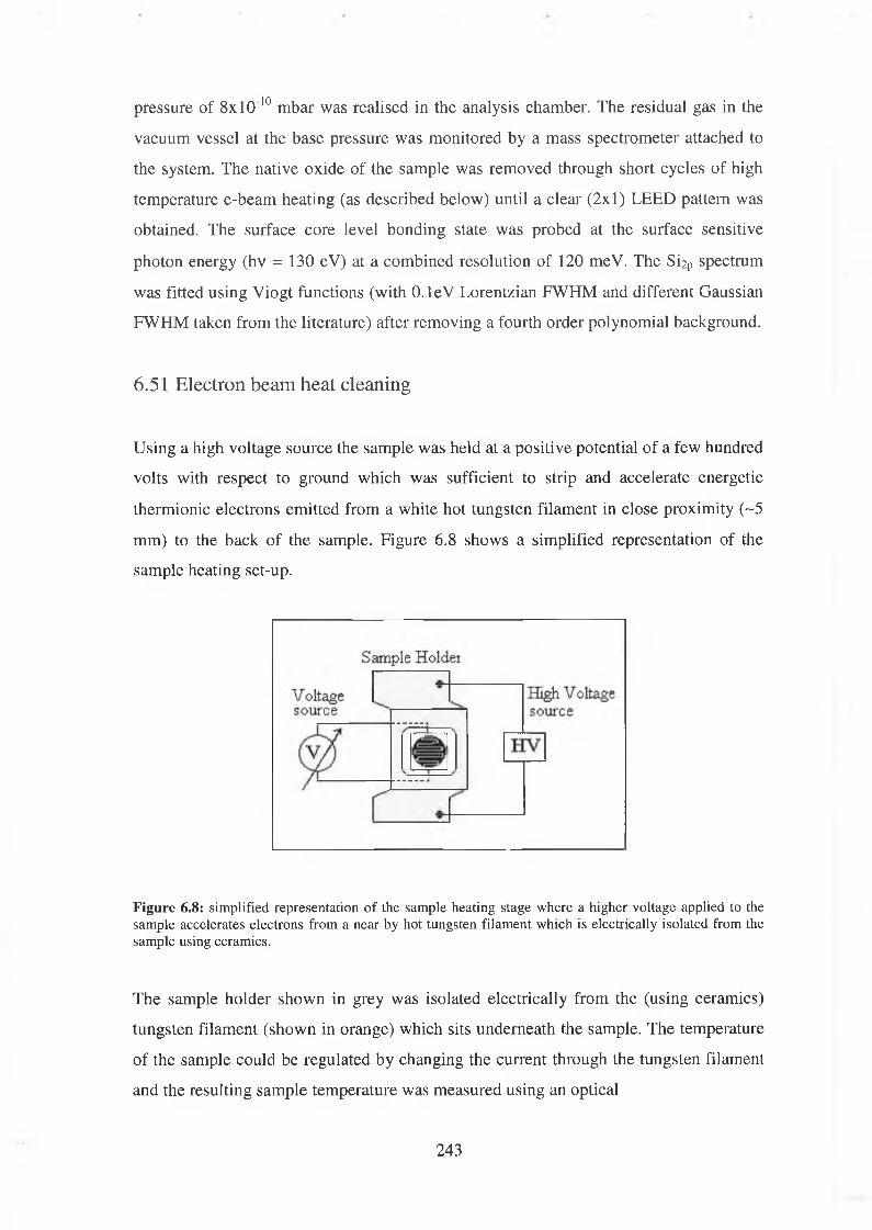
pressure of 8x10 10 mbar was realised in the analysis chamber. The residual gas in the
vacuum vessel at the base pressure was monitored by a mass spectrometer attached to
the system. The native oxide of the sample was removed through short cycles of high
temperature e-beam heating (as described below) until a clear (2x1) LEED pattern was
obtained. The surface core level bonding state was probed at the surface sensitive
photon energy (hv = 130 eV) at a combined resolution of 120 meV. The Si2P spectrum
was fitted using Viogt functions (with O.leV Lorentzian FWHM and different Gaussian
FWHM taken from the literature) after removing a fourth order polynomial background.
6.51 Electron beam heat cleaning
Using a high voltage source the sample was held at a positive potential of a few hundred
volts with respect to ground which was sufficient to strip and accelerate energetic
thermionic electrons emitted from a white hot tungsten filament in close proximity (~5
mm) to the back of the sample. Figure 6.8 shows a simplified representation of the
sample heating set-up.
Figure 6.8: simplified representation of the sample heating stage where a higher voltage applied to the sample accelerates electrons from a near by hot tungsten filament which is electrically isolated from the sample using ceramics.
The sample holder shown in grey was isolated electrically from the (using ceramics)
tungsten filament (shown in orange) which sits underneath the sample. The temperature
of the sample could be regulated by changing the current through the tungsten filament
and the resulting sample temperature was measured using an optical
243
pyrometer. At a potential of 600 V, ramping the filament current to and holding it (for
10 second intervals) at 6 Amps caused the sample to glow white-hot and realised a
temperature of -1130 C°. At this temperature the native oxide is desorbed along with
hydrocarbon contamination. The base pressure during heat cleaning cycles was only
ever allowed to rise to 8xl0"8 mbar. After a series of heat cleaning cycles the oxide was
removed and a well ordered (2x1) LEED pattern was obtained.
6.52 Sulphur Cell [21]
Tantalum /shield
Sulphur Cell
<— Glass chimney
Platinum Mesh
Tungstenheatingelement
Silver Powder
Figure 6.9: A schematic illustration of the electrochemical sulphur source
244
Figure 6.9 shows a diagram of the sulphur cell mounted on a knife-edge flange with
electrical feedthroughs. The cell was made from a compressed pellet by pressing
powders of silver (Ag), silver iodide (Agl) and silver sulphide (AgS2) together between
two sheets of platinum mesh. The pellet sits into the glass chimney with electrical
contacts made to the front and back end of the pellet. The chimney is surrounded by a
sheet of tantalum, which is heated radiativity by passing a suitable current (~ 6 A)
through the exterior tungsten wire which is wrapped into a helical coil. The hot tantalum
sheet then uniformly heats the pellet. When heated to approximately 200 °C an electrical
potential of 200 meV exists across the cell. By applying a suitable bias to the cell a
constant current (20 |iA) is established by a constant current source. This current is
facilitated by the silver sulphide acting as a ionic conductor, with Ag+ ions flowing
towards the silver iodide pellet. Molecular sulphur effuses from the throat of the
chimney given the local concentration of sulphur. The clean surface is located (in line of
sight) a few cm away from the top of the chimney. Figure 6.10 shows a photograph of
the inside of the analysis chamber as seen during S deposition.
Figure 6.10: A photograph of the inside of the analysis chamber
The silicon sample has been mounted onto the substrate heater with tantalum clips and
is visibly hot. On the left is the mass spectrometer head. On the right is the lens of the
245

analyser. The LEED system is in the background and is protected by its shutter. Finally
the glass chimney of the sulphur cell is visible protruding from below.
6.53 Clean Si(100)
h v = 130 eV
1 r2 1 2 2 2 3 2 4
Relative Kinetic Energy (eV)
Si(100)-(2xl)
Figure 6.11: (Top) surface core level shifts in Si2p spectrum at hv = 130 eV. (Bottom [22]) ball and stickrepresentation of outer surface geometric surface.
Having “burned o ff’ the native oxide and established a well ordered (2x1) LEED
pattern, the Si2P core-level spectrum was measured at a photon energy of 130 eV. Figure
246
6.11 shows the resulting spectrum. The experimental data is shown in black and the fit
in red. The spectrum was fitted using a least squares fitting routine with five Voigt
peaks who’s Lorentzian width was fixed at 100 meV, a value of 250 meV was used for
the Gaussian FWHM (as used by Landemark et al [22] and Pi et al [23]). A branching
ratio of 2 and spin-orbit split of -0.6 eY were consistently found to provide the best fit.
The background was fitted with a Shirley background. The magnitude of the chemical
shifts to higher (two components) and lower (two components) kinetic energy relative to
the substrate component were found to be +161 meV (peak C), + 591 meV (peak S) and
-155 meV (peak SS), -289 meV (peak S’). Resolution limitations prevented us from
distinguishing between the precise assignments of these components as proposed by
Landemark [22] and Pi [23].
6.54 Sulphur Deposition
The sample temperature was brought to 1130 K by slowly increasing the current in the
heating filament while the sample was held at a potential of +600V. With the sample
facing away from the sulphur cell, the cell was heated to 200 °C and when the cell
potential was established a current of 20 ^A was passed through it. The pressure in the
main chamber rose to 5 x 1 O'7 mbar, a large sulphur signal was evident from the mass
spectrometer display and was the dominant contributor to the pressure increase. Next
the sample was turned to face into the sulphur flux for 5 mins. The sample temperature
was gradually reduced and allowed to cool in the sulphur flux. Figure 6.12 shows the
Si2P core level spectrum taken from the sample at a photon energy of 130 eV at normal
incidence and at 60° off normal respectively. The spectra of the sulphur treated surface
could be consistently fitted with one bulk and two chemically shifted surface
components of approximately equal magnitude shifted by 0.53 and 1.2 eY to higher
binding energy. These chemical shifts were assumed to correspond to silicon atoms at
the surface in the +1 and +2 oxidation state. While the chemically shift associated with
the +2 oxidation state at 1.2 eV was consistent with that reported by Weser et al [24],
the +1 oxidation state had a lower chemical shift. This however could be due to strain
effects in the local surface structure resulting in a modification of the electronic
structure as their method of surface preparation is different from ours.
247

21 2 2 2 3 2 4 2 6 2 6
Relative Kinetic Energy [eV]
Figure 6.12: De-convolution of Si2P oxidation states for the sulphur treated (5 min dose) surface at hv=130 eV for (a) normal emission and (b) 60° off normal on Si(100).
Take-off Angle (0) Si1+ % Bulk Sii+ % Bulk Si1+ % Si
0 25.5 36.5 89
60 42.3 64 85
Table 6.0: Si2p peak intensities for normal and 60 off angle scans.
Table 6.0 summarises the peak intensities for the normal and 60° off normal scans. The
relative intensities of the two oxidation states is independent of angle suggesting that
248
both components are located in the same surface plane and exist in the outer most plane.
LEED analysis of the surface indicates that the surface displays a bulk like ( lx l) surface
termination. The lifting of the (2x1) surface structure suggests that the surface dimers
have been broken.
Figure 6.13 shows the sulphur 2p core level spectrum taken at normal incidence at a
photon energy of 190 eV. The peak was fitted using a branching ratio of two, a
Gaussian FWHM of 0.47 eV and a spin-orbit split of 1.15 eV.
Kinetic Energy (eV)
Figure 6.13: Core-level photoemission spectrum of the S2p peak from the sulphur treated (5 min d ose)surface at hv=190 eV on Si(100) ( lx l) .
A good fit could only be obtained using a single peak which was identical to that
obtained at 60° off normal. This suggested that sulphur existed in a unique chemical
environment at the surface. Our fitting parameters were similar to those reported by
Mullins et al [25] for the interaction of sulphur with the tungsten surface in which the
sulphur resides in a single chemical phase for coverages of less than half a monolayer.
In order to properly interpret the surface termination the existence of sulphur in a single
chemically shifted component while the silicon substrate spectra displays two
249

chemically shifted interface peaks of approximately equal intensity needs to be
resolved.
6.55 Discussion o f results
It is useful to precede our interpretation of the above results by first comparing them
with those of others in the literature. Earlier it was mentioned that the restoration of the
( lx l) bulk periodicity and passivation of the Si(100) surface with sulphur was until
recently only a theoretical possibility. Papageorgopoulos et al [26] reported the
successful room temperature deposition of elemental sulphur on Si(100) restoring the
surface (2x1) periodicity back to a (lx l). Previously Weser investigating the behaviour
of S on Si(100) had not been able to observe an ordered overlayer. Moriarty et al [27]
reported that room temperature adsorption of sulphur on silicon resulted in the
formation of an overlayer with the underlying Si(100) retaining the (2x1)
reconstruction. On annealing the S/Si( 100)2x1 surface to 325 °C desorption of the
sulphur overlayer occurred with the appearance of a coexisting c(4x4) and (2x1) surface
reconstructions.
Papageorgopoulos [26] proposed, from consideration of the change in slope of the S
Auger peak-to-peak heights as a function of the number of sulphur doses and from
LEED analysis that for low sulphur does, S adatoms initially reside on the dimers in
bridge sites with each S atom bonded through the dangling bonds forming a half
monolayer (2x1) coverage as shown in Figure 6.14 (B). Figure 6.14 (A) shows the clean
reconstructed Si(l 00)2x1 surface. For coverages above Vi a monolayer the Si dimers are
broken providing bonding for the sulphur atoms. The silicon atoms are displaced
resulting in the restoration of the ( lx l) bulk termination. The sulphur adatoms remain in
bridge sites and are bound to neighbouring Si atoms as shown in Figure 6.14 (C). For
coverages between 1 and 2 monolayers sulphur is embedded into the Si substrate
through diffusion as shown in Figure 6.14 (D).
However Hahn et al [28,29] reported that they were unable to reproduce the results of
Papageorgopoulos but did however obtain a Si(100)-(lxl) termination by exposing the
surface to a beam of sulphur at elevated temperatures in a method similar to ours.
250

Bringans and Olmstead [30,31] reported results of a photoemission study of selenium
and ZnSe interactions with the Si(100) surface in an investigation of heteroepitaxial
growth on elemental semiconductors.
0 0 0 0 0 0 . 0< § • # # < § > • ©OOOO O OO
(c)
(b)
S u lp h u r
unjderlsyer
oooeooo©o@o@o©O O O O O O O
(d) ©0©0©0O
oSo^oio
Figure 6.14: (a) clean reconstructed Si(100)2xl, b) the S-(2xl) (hemisulfide) structure on the Si(100)2xl surface, c) the S -( lx l) (monosulfide) structure on a Si(100)lxl surface and d) the diffused second S layer into the bulk o f S i(100)lx l (Papageorgopoulos [26]).
They concluded from their core level spectra that only a half of the topmost silicon
atoms are bonded to two Se atoms, with the other half bonded to one Se atom. This
indicated that the surface coverage of Se corresponded to 3/4 monolayer of Se atoms in
the bridge position. What is interesting about this submonolayer-covered surface, in the
251
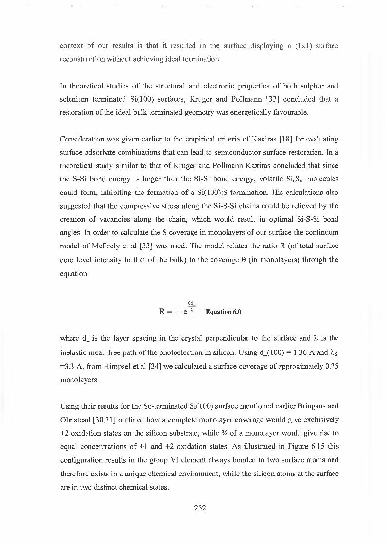
context of our results is that it resulted in the surface displaying a ( lx l) surface
reconstruction without achieving ideal termination.
In theoretical studies of the structural and electronic properties of both sulphur and
selenium terminated Si(100) surfaces, Kruger and Pollmann [32] concluded that a
restoration of the ideal bulk terminated geometry was energetically favourable.
Consideration was given earlier to the empirical criteria of Kaxiras [18] for evaluating
surface-adsorbate combinations that can lead to semiconductor surface restoration. In a
theoretical study similar to that of Kruger and Pollmann Kaxiras concluded that since
the S-Si bond energy is larger than the Si-Si bond energy, volatile SinSm molecules
could form, inhibiting the formation of a Si(100):S termination. His calculations also
suggested that the compressive stress along the Si-S-Si chains could be relieved by the
creation of vacancies along the chain, which would result in optimal Si-S-Si bond
angles. In order to calculate the S coverage in monolayers of our surface the continuum
model of McFeely et al [33] was used. The model relates the ratio R (of total surface
core level intensity to that of the bulk) to the coverage 0 (in monolayers) through the
equation:
9d,
R = 1 — e 1 Equation 6.0
where dj. is the layer spacing in the crystal perpendicular to the surface and X is the
inelastic mean free path of the photoelectron in silicon. Using dj_(100) = 1.36 A and Xsi
=3.3 A, from Himpsel et al [34] we calculated a surface coverage of approximately 0.75
monolayers.
Using their results for the Se-terminated Si(100) surface mentioned earlier Bringans and
Olmstead [30,31] outlined how a complete monolayer coverage would give exclusively
+2 oxidation states on the silicon substrate, while 3/4 of a monolayer would give rise to
equal concentrations of +1 and +2 oxidation states. As illustrated in Figure 6.15 this
configuration results in the group VI element always bonded to two surface atoms and
therefore exists in a unique chemical environment, while the silicon atoms at the surface
are in two distinct chemical states.
252
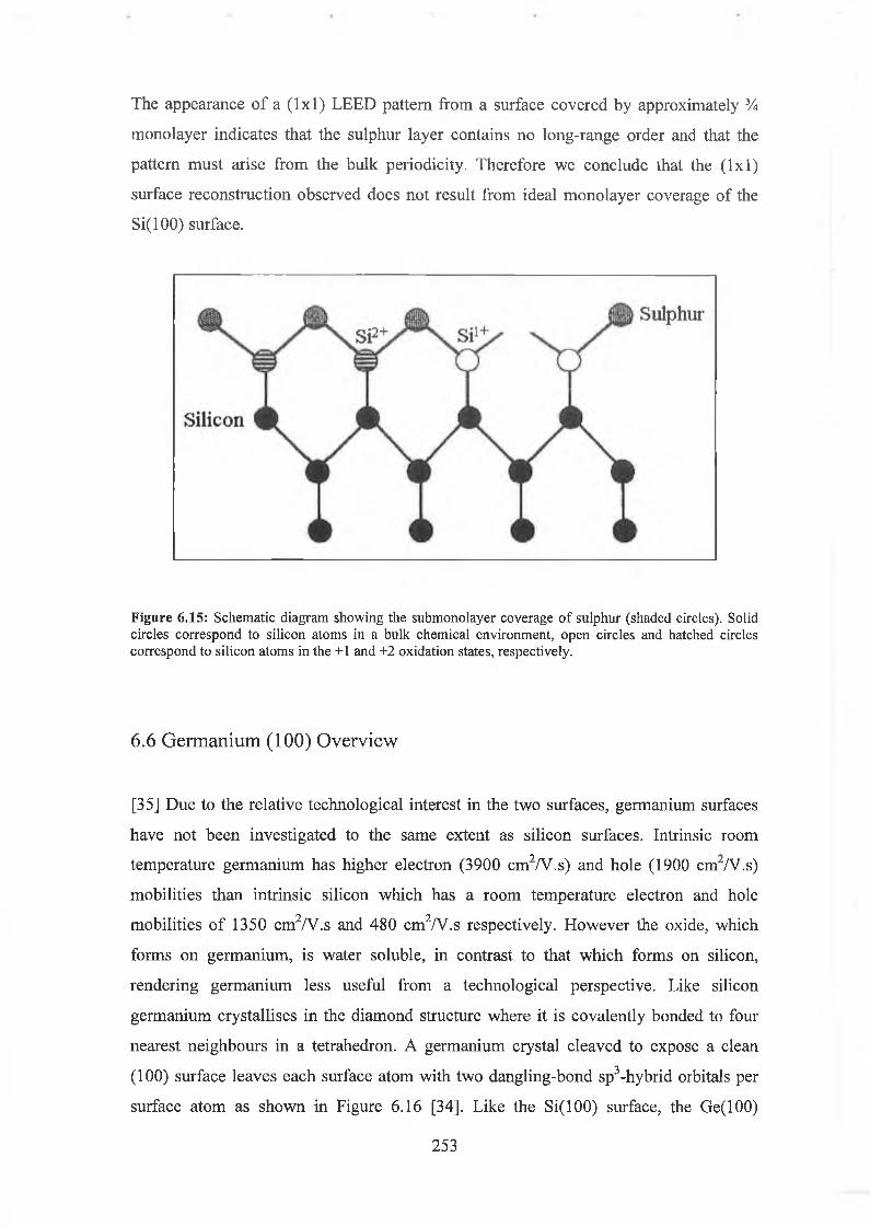
The appearance of a ( lx l) LEED pattern from a surface covered by approximately 3A
monolayer indicates that the sulphur layer contains no long-range order and that the
pattern must arise from the bulk periodicity. Therefore we conclude that the ( lx l)
surface reconstruction observed does not result from ideal monolayer coverage of the
Si(100) surface.
Figure 6.15: Schematic diagram showing the submonolayer coverage o f sulphur (shaded circles). Solid circles correspond to silicon atoms in a bulk chemical environment, open circles and hatched circles correspond to silicon atoms in the +1 and +2 oxidation states, respectively.
6.6 Germanium (100) Overview
[35] Due to the relative technological interest in the two surfaces, germanium surfaces
have not been investigated to the same extent as silicon surfaces. Intrinsic room'ytemperature germanium has higher electron (3900 cm /V.s) and hole (1900 cm /V.s)
mobilities than intrinsic silicon which has a room temperature electron and hole
mobilities of 1350 cm2/V.s and 480 cm2/V.s respectively. However the oxide, which
forms on germanium, is water soluble, in contrast to that which forms on silicon,
rendering germanium less useful from a technological perspective. Like silicon
germanium crystallises in the diamond structure where it is covalently bonded to four
nearest neighbours in a tetrahedron. A germanium crystal cleaved to expose a clean
(100) surface leaves each surface atom with two dangling-bond sp3-hybrid orbitals per
surface atom as shown in Figure 6.16 [34]. Like the Si(100) surface, the Ge(100)
253
surface reconstructs through the pairing of surface atoms to form rows of asymmetric
dimers along the [110] crystallographic directions. In STM studies [36] the orientation
of the reconstruction was found to rotate through 90° between (2x1) terraces that were
separated by monatomic step heights as expected for the rotation of the tetrahedral
dangling bonds by 90° between terrace domains.
Ge(100) Surface
(J) Top Layer Atom
# Second Layer Atom
Figure 6.16: Plan view o f the bulk terminated (100) surface. Each surface atom is left with two dangling- bond orbitals. The tetrahedral dangling-bonds on the second layer atoms are rotated by 90° with respect to the surface normal from the top layer o f tetrahedral bonds. This bond rotation leads to a surface with two domains, after undergoing a (2x1) pairing reconstruction, where the two domains are separated by monatomic height steps [34].
This multi-domain structure gives rise to the (2x1) LEED pattern like silicon and it
minimises the elastic energy in the substrate. In addition to the half order LEED spots
expected for the two-domain (2x1) dimer reconstruction, weak quarter-order spots have
also been observed in room temperature measurements by Fernandez et al [37] of the
surface indicating the existence of higher order domains ( ie (4x2) ). The first room
temperature STM images by Kubby et al [35] of Ge(100) found it to be composed of
asymmetric dimers that did not require defects to quench the surface dynamics in
contrast to the room temperature Si(100) surface.
254

6.61 Clean Ge(100)-(2xl) SCLS
In investigating the surface core level shift of the Si(100)-(2xl) surface Landemark et al
[22] enjoyed an excellent resolution of 70 meV facilitating the identification of 4
chemical states corresponding to the up dimer atoms (S), the down dimer atoms (SS),
the atoms in the second layer (S’) and half of the third layer atoms (C). Despite this,
their convergence on a final consistent peak parameter set was only made after detailed
analysis of the stability of the bulk peak position while fitting with three surface peaks
(in order to elucidate the presence of the fourth) as not all peaks are apparent from the
spectrum envelope. The experimental resolution obtained for the Ge(100) 3d core-level
spectra has been lower than that obtained for Si(100) 2p data and there is no general
consensus about how many surface related components are present in the Ge 3d core
level photoemission spectra. Schnell et al [38] fitted the Ge(100) spectrum using only
one surface component, shifted by — 0.45 eV with respect to the bulk component, due
to one monolayer of both up and down dimer atoms. Chen et al [39] also used only one
surface component but argued that two separate components should be expected
because of the charge transfer from the down atom to the up atom in the same dimer. He
associated the observed surface core level shift with Vi a monolayer of up atoms, while
the down atom component was assumed to overlap the bulk contribution. LeyLay et al
[40] and others [41,42] have used two surface components, besides the lower binding
energy doublet at -0.54 eV with respect to the bulk they found a second core level
shifted by -0.19 eV. However, the dimer bonding is interpreted as covalent and the
second component is attributed to emission from the subsurface layer. In the ionic
model of Chen [39] the second component is attributed to charge transfer from the down
atom emission.
In order to elucidate the number of surface core level peaks Goldoni et al [43] have
undertaken difference spectra analysis of the Ge3d spectrum in order to remove a
suitable weighted bulk component numerical, from a surface sensitive spectrum, thus
leaving the surface core level shifts. Figure 6.17(a) shows the Ge3d spectra taken at
photon energies of 45 eV (at normal emission) and 70 eV (at 70° off normal) which
yield bulk and surface sensitive information respectively. Figure 6.17(b) shows the
spectra after background subtraction and having been normalised to the same area.
255
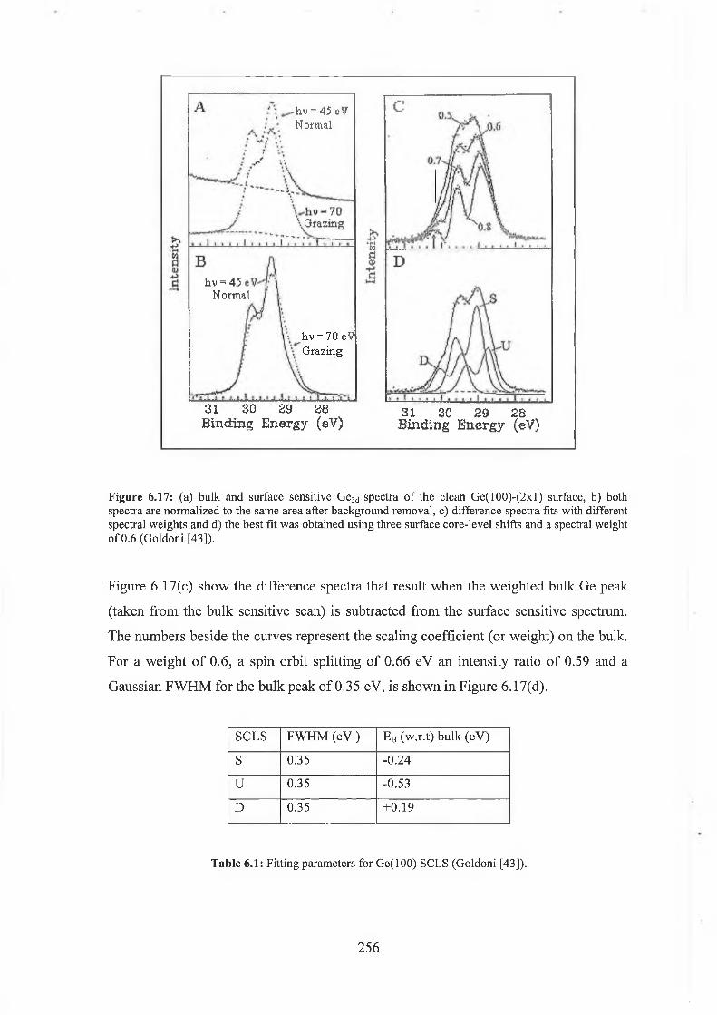
31 SO S9 sa Binding Energy (eV)
31 3 0 2 9 2 8Binding E nergy (eV)
-hv = 45 eV Normal
hv = 45 Normal
hv = 7 0 eV Grazing
Figure 6.17: (a) bulk and surface sensitive Ge3d spectra o f the clean G e(100)-(2xl) surface, b) both spectra are normalized to the same area after background removal, c) difference spectra fits with different spectral weights and d) the best fit was obtained using three surface core-level shifts and a spectral weight of 0.6 (Goldoni [43]).
Figure 6.17(c) show the difference spectra that result when the weighted bulk Ge peak
(taken from the bulk sensitive scan) is subtracted from the surface sensitive spectrum.
The numbers beside the curves represent the scaling coefficient (or weight) on the bulk.
For a weight of 0.6, a spin orbit splitting of 0.66 eV an intensity ratio of 0.59 and a
Gaussian FWHM for the bulk peak of 0.35 eV, is shown in Figure 6.17(d).
SCLS FWHM (eV ) Eb (w.r.t) bulk (eV)
S 0.35 -0.24
U 0.35 -0.53
D 0.35 +0.19
Table 6.1: Fitting parameters for Ge(100) SCLS (Goldoni [43]).
256
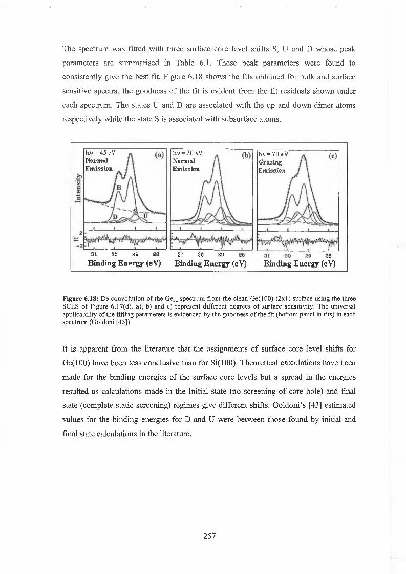
The spectrum was fitted with three surface core level shifts S, U and D whose peak
parameters are summarised in Table 6.1. These peak parameters were found to
consistently give the best fit. Figure 6.18 shows the fits obtained for bulk and surface
sensitive spectra, the goodness of the fit is evident from the fit residuals shown under
each spectrum. The states U and D are associated with the up and down dimer atoms
respectively while the state S is associated with subsurface atoms.
31 3 0 2 9 a s
Binding Energy (eV)SI 30 S3
Binding Energy (eV) Binding Energy (eV)
hv = 45 eVNormalEmission
hv = 7 0 eVNormalEmission
hv = 7 0 eVGrazingEmission
Figure 6.18: De-convolution of the Ge3d spectrum from the clean Ge(100)-(2xl) surface using the three SCLS o f Figure 6.17(d). a), b) and c) represent different degrees o f surface sensitivity. The universal applicability o f the fitting parameters is evidenced by the goodness o f the fit (bottom panel in fits) in each spectrum (Goldoni [43]).
It is apparent from the literature that the assignments of surface core level shifts for
Ge(100) have been less conclusive than for Si(100). Theoretical calculations have been
made for the binding energies of the surface core levels but a spread in the energies
resulted as calculations made in the Initial state (no screening of core hole) and final
state (complete static screening) regimes give different shifts. Goldoni’s [43] estimated
values for the binding energies for D and U were between those found by initial and
final state calculations in the literature.
257

6.62 S Passivation of Ge(100)
In this thesis sulphur passivation has been investigated by deposition of molecular S
using the flux from an electrochemical cell. Sulphur has also been deposited in-suitu
using HS2 gas and ex situ wet chemically using NHS4. H2S adsorption on Si(100) is
believed to be dissociative and leads to co-adsorption of H2S H and S [44]. Kuhr and
Ranke [45] investigating the adsorption of H2S on Ge(100) found it to be dissociative,
they identified SH and S using photoemission. Leung et al [46], by monitoring the Ge/S
auger intensity achieved a S saturation coverage of Ge(100) after successive cycles of
dosing and annealing at 350°C. They concluded from the disappearance of Ge-H and S-
H related peaks in separate electron energy loss spectroscopy measurements, that
annealing at 350°C leads to the desorption of H leaving S on the surface. They proposed
that S starts to desorb at 370°C. However, despite this there is uncertainty about the
temperature at which S desorbs and also it has been proposed that H cannot be removed
selectively [17]. In chapter 4 the wet chemical passivation of Si was considered by the
removal of it’s native oxide and the termination of its dangling bonds with hydrogen
using HF. Urhberg et al [47] have undertaken soft X-ray synchrotron photoemission
analysis of the hydrogen terminated surface and concluded that the adsorbed H bonds to
the surface dangling bonds resulting in a symmetric dimer reconstruction. Similarly
Anderson et al [48] have investigated the S passivation of Ge wet chemically using
aqueous ammonium sulphide (NFL^S. Others have sought to engineer a flux of
elemental S insitu using by evaporating sulphur from a tungsten filament [23] or by
molecular beam epitaixy. An electrochemical cell performs well as a source of a large
flux of molecular sulphur but as pointed out by Gothelid [47] can behave non-uniform
in its delivery over the course of sample dosing.
In a theoretical study of the structural and electronic properties of sulphur terminated
Ge(100), Kruger and Pollmann [49] concluded that a restoration of the ideal bulk
terminated geometry was energetically favourable with the sulphur atoms occupying
bridge bond sites between neighbouring surface Ge atoms. Weser and Bogen [17]
investigated room temperature deposition of molecular sulphur using core level
photoemission, Auger electron spectroscopy and LEED. Using an electrochemical cell
they reported the “ideal monolayer termination” of Ge(100)-(2xl) surface at room
temperature with the restoration of the ( lx l) bulk termination. Figure 6.19(a) shows the
258
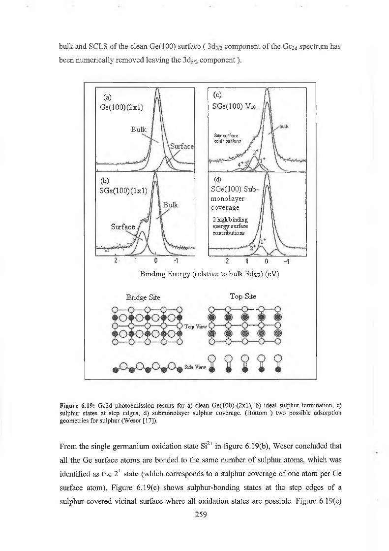
bulk and SCLS of the clean Ge(100) surface ( component of the Ge3d spectrum has
been numerically removed leaving the 3 ds/2 component).
(a)Ge(100) (2x1)
Bulk
(b)SGe(100)(lxl)
Surface
(c)SGe(lOO) Vic.
fou* surface contributions
(d)SGe(lOO) Submonolayercoverage2 highbinding energy surface contributions
1 0 *1 2 1 0 - 1
Binding Energy (relative to bulk 3dsri) (eV)
Bridge Site Top Site
Top
Figure 6.19: Ge3d photoemission results for a) clean G e(100)-(2xl), b) ideal sulphur termination, c) sulphur states at step edges, d) submonolayer sulphur coverage. (Bottom ) two possible adsorption geometries for sulphur (Weser [17]).
From the single germanium oxidation state Si2+ in figure 6.19(b), Weser concluded that
all the Ge surface atoms are bonded to the same number of sulphur atoms, which was
identified as the 2+ state (which corresponds to a sulphur coverage of one atom per Ge
surface atom). Figure 6.19(c) shows sulphur-bonding states at the step edges of a
sulphur covered vicinal surface where all oxidation states are possible. Figure 6.19(e)
259

show the two possible bonding geometries for sulphur. As the bridge site corresponds to
single bonds (S-Ge) and the top site corresponds to double bonds (S=Ge), the two
different bond models were distinguished by Weser from investigation of low S
coverages. Namely in the absence of island formation, two oxidation states (1+ and 2+)
are expected for bridge adsorption and only one oxidation state (+2) for top site
adsorption. Figure 6.19(d) shows the spectrum for room temperature low S coverages,
which show two surface contributions, dominated by the 1+ oxidation state suggesting
that S is bridge bonded with no large sulphur islands formed.
6.63 S/Ge(l 00) Experimental
Soft X-ray photoemission analysis was performed on beamline U4A at the NSLS.
Germanium (100) substrates (p type 1-2 Qcm ) were used. A flux of molecular sulphur
was realised as described earlier using a UHV compatible electrochemical S cell. The
germanium lattice cannot sustain the same degree of aggressive heating which is used to
clean Si and so successive cycles of mild (0.6-0.8 keV) Ar+ ion sputtering and
annealing at 600 °C were used until a well ordered (2x1) LEED pattern was obtained.
The core level bonding states of the surface were probed at the surface sensitive photon
energy (hv=70 eV) at a combined resolution (monochromator + analyzer) of 200 meV.
The Ge3d spectrum was fitted using Voigt functions (with 0.1 eV Lorentzian FWHM
and different Gaussian FWHM). The fitting parameters are based on those used by
Goldini [43] as described earlier. Figure 6.20 shows our fit for the clean Ge(100)-(2xl)
surface. The raw data is shown in red and the fit in black. Table 6.2 summarises the
fitting parameters.
260
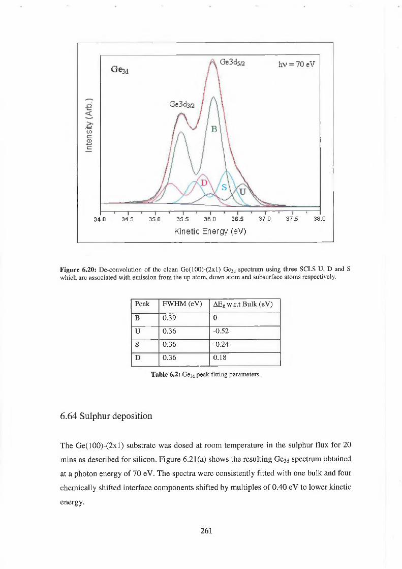
34.0 34.5 35.0 35.5 36.0 36.5 37.0 37.5 38.0
Kinetic Energy (eV)
Figure 6.20: De-convolution of the clean Ge(100)-(2xl) Ge3d spectrum using three SCLS U, D and S which are associated with emission from the up atom, down atom and subsurface atoms respectively.
Peak FWHM (eV) AEb w.r.t Bulk (eV)
B 0.39 0
U 0.36 -0.52
S 0.36 -0.24
D 0.36 0.18
Table 6.2: Ge3d peak fitting parameters.
6.64 Sulphur deposition
The Ge(100)-(2xl) substrate was dosed at room temperature in the sulphur flux for 20
mins as described for silicon. Figure 6.21(a) shows the resulting Ge3d spectrum obtained
at a photon energy of 70 eV. The spectra were consistently fitted with one bulk and four
chemically shifted interface components shifted by multiples of 0.40 eV to lower kinetic
energy.
261
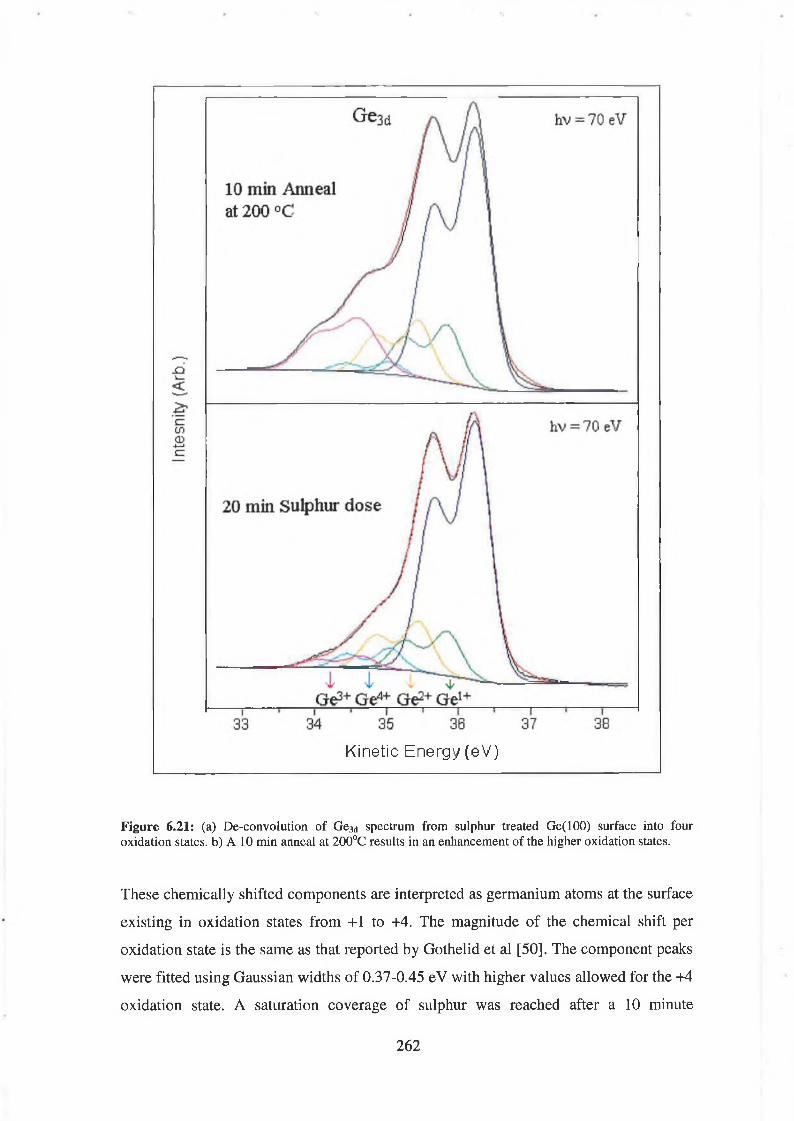
Kinetic E ne rgy (eV)
Figure 6.21: (a) De-convolution of Ge3d spectrum from sulphur treated Ge(100) surface into four oxidation states, b) A 10 min anneal at 200°C results in an enhancement of the higher oxidation states.
These chemically shifted components are interpreted as germanium atoms at the surface
existing in oxidation states from +1 to +4. The magnitude of the chemical shift per
oxidation state is the same as that reported by Gothelid et al [50]. The component peaks
were fitted using Gaussian widths of 0.37-0.45 eV with higher values allowed for the +4
oxidation state. A saturation coverage of sulphur was reached after a 10 minute
262
exposure to sulphur from the electrochemical cell after which a bulk like ( lx l) LEED
pattern was observed. The lifting of the (2x1) surface structure following sulphur
treatment is consistent with the breaking of the surface dimers. However unlike Weser
et al [17] we observed all four oxidation states as opposed to just the +2 characteristic of
the ideal termination by a monolayer of sulphur atoms occupying bridge positions.
Gothelid et al [50] reported that at saturation coverage (which they estimated to be
above one monolayer) there are contributions from all four oxidation states. They
explained the presence of higher oxidation states by the fact that sulphur etches the
surface to produce a stripped character with a high density of monatomic steps, as seen
in STM analysis by his group. The ratio of the intensity of the chemically shifted
components to the bulk substrate peak 38:62 indicate that the saturation coverage was in
excess of a monolayer in agreement with Gothelid. From analysis of the relative
intensities, the +2 oxidation state intensity was found to dominate, which corresponds to
adsorbed sulphur atoms occupying bridge sites between neighbouring atoms. The above
experimental observations suggest that the ( lx l) LEED pattern observed for the sulphur
covered surface originated from the underlying bulk structure and not from an ordered S
overlayer.
Figure 6.22 shows the evolution of the S2p spectrum with sulphur dose and final anneal
as reported by Gothelid [50] . He attributed the high binding energy (low kinetic
energy) component A2 to a non-reacted surface component, which disappeared upon
annealing. Figure 6.23 (a) and (b) shows our S2P spectra after 10 min deposition and
subsequent anneal at 200°C respectively. We also attribute the low kinetic energy
component to a non-reacted S component, which de-absorbs after annealing the surface.
Annealing of our sulphur treated surface at 200°C for 10 minutes resulted in a
significant increase in the intensity of the Ge +4 oxidation state (see Figure 6.21(b)) and
a corresponding increase in the ratio of surface to substrate intensity from 38:62 to
47:53. This increase was most likely caused by the incorporation of some of the non-
reacted sulphur on the surface and is consistent with the formation of a thicker reacted
phase layer between the sulphur and germanium, possibly a GeS2 reacted layer. Similar
changes were reported in the distribution of oxidation states following the annealing of
the oxygen covered surface by Himpsel et al [51]. Bringans and Olmstead [30] also
reported the presence of 4 oxidation states following the thermal annealing of a
deposited selenium layer on the Si(100) surface, with the +4 state being the dominant
263
component. They interpreted the result as indicating the formation of a SiSe2 layer at the
surface.
Figure 6.22: S2p spectra following room temperature sulphur deposition and annealing o f the Ge(100) substrate. Two contributions were observed, A1 and A2. (Gothelid [50])
The presence of +3 and +4 oxidation states following room temperature adsorption is
indicative of sulphur bonding to surface steps and imperfections, the number of which
can depend on the surface preparation procedure. After annealing the sulphur covered
surface to temperatures higher than 200 °C a reduction of the intensity of the chemically
shifted components was observed and ultimately the complete removal of the adsorbed
sulphur layer and the re-establishment of the clean surface (2x1) reconstruction. The S2P
spectrum, following the 200 °C anneal in Figure 6.23 was significantly broader than the
corresponding spectrum for the same peak observed on the sulphur terminated Si(100)
surface.
264

Kinetic Energy (eV)
Figure 6.23: (a) S2p spectrum after 20 min dose, there sulphur is in a multi-bonding environment (b) the low kinetic energy S contribution has been removed following a 10 min anneal at 200 °C
This is reasonable given that the analogous Ge3d spectrum still contained 4 oxidation
states, indicating that the near surface germanium atoms were in a range of different
chemical environments. Recent STM and thermal desorption studies [52] support the
assertion by Gothelid [50] that the thermal annealing of the sulphur covered surfaces
leads to the desorption of surface germanium atoms in an etching process. These results
are consistent with our experimental observations of preferential compound formation
following thermal annealing.
6.65 Discussion o f results
The deposition of sulphur onto the Ge(100) surface at room temperature lead to the
breaking of the surface dimers and the termination of the surface in a chemically reacted
S-Ge layer of one to two monolayers thick. Following an anneal at 200°C, this reacted
phase predominately consisted of GeS2. The surface termination was therefore non-ideal
and the ( lx l) LEED pattern was ascribed to the bulk structure being observed through a
265
disordered layer. Annealing at higher temperatures resulted in the desorption of sulphur,
restoring the clean (2x1) surface reconstruction.
6.7 Conclusion
From consideration of the results of the literature and our own attempts to realise an
ideal monolayer termination of the surfaces of Si(100) and Ge(100) with sulphur it is
apparent that the passivation of these surfaces with a single monolayer is possibly
unattainable. The body of work in the literature is finite and diverse in that a wide
variety of passivation procedures have been tried, but are not exhaustive. The point is
borne out by the SÍO2 core level findings of chapter 4 where despite 20 years of
dedicated optimisation the non-idealness of the SÍO2 interface, manifested by the
existence of an interfacial SiOx, is inherent in the oxidation process.
Theoretical studies in deciding the suitability of sulphur as a candidate for passivation
Si(100) and Ge(100) surfaces are encouraging except in respect of the larger bond
length and energies for S-Si bonds compared to Si-Si bonds and the volatile bonding
interaction of S and germanium. It is on this theoretical basis that the co-existence of the
single S2P phase with the two oxidation states of silicon was reconciled. In other words
the adsórbate induced strain is relaxed through the formation of optimal Si-S bond
angles which is facilitated by vacancies in the surface S coverage. Analogously for
Ge(100) the increased complexity of the surface structure manifested by the presence of
all four oxidation states is attributed to the volatile S-Ge bonding interaction resulting in
the surface being etched.
Synchrotron radiation has played a valuable role in investigating both the bonding
chemistry and geometry of the outer surface through the surface core level shifts.
However, from the literature and our analysis of the SÍ/SÍO2 system we are mindful of
the need to characterise photoemission results in the context of a samples history, which
for surface passivation starts, with the engineering of the clean surface. Therefore for
future work where Si(100) and Ge(100) surfaces are passivated through a more
optimised procedure, complementary techniques such as FTIR and STM could be
employed along with synchrotron radiation analysis facilitating a more complete
characterisation.
266

6.8 References for Chapter VI
1 Taken from the web elements online book store http://www.webelements.com/
2 Chemistry, 3 rd Ed, Me Murry (Prentice Hall) page 275
3 S. Hasegawa, X. Tong, S. Takeda, N. Sato, Prog. Surf. Sei. 60 (1999) 89
4 C. Duke, Appl. Surf. Sei. 65/66 (1993) 543, Also C. Duke, Scanning Micros.
8(1994) 743
5 Silicon Surfaces and formation of interfaces, J. Dabrowski, H. J. Mussig World
scientificpage 90
6 H. Farnsworth, R. Schlier, T. George, R. Burger, J. Appl. Phys. 29 (1958) 1150
7 R. Tromp, R. Hamers, J. Demuth, Phys. Rev. Letts 55, (1985) 1303
8 J. Dabrowski, M. Scheffler, Appl. Surf. Sei. 56 (1992) 15
9 M. Rohlfing, P. Kruger, J. Pollmann, Phys Rev B 52 (1995) 13753
10 D. Chadi, Phys Rev Lett, 43 (1979) 43
11 Courtesy of the G. Hughes A. Coffola, D. Carty, P Gauano, Surface science group,
DCU
12 R. Uhrberg, E. Landemark, Y. Chao, J. Elect. Spect. Relt. Phen. 75 (1995) 197
13 R. Bringans, R. Uhrberg, R. Bachrach, J. Northrup, Phys. Rev. Lett. 55(1985) 533
14 M. Olmstead , R. Bringans, R. Uhrberg, R. Bachrach, Phys. Rev. B 34 6041 (1986)
6041
15 R. Uhrberg, R. Bringans, M. Olmstead, Phys. Rev. B 35 (1987) 3945
16 R. Uhrberg, R. Bringans , R. Bachrach, J. Northrup, Phys. Rev. Lett. 56 (1986) 520
17 T. Weser, A. Bogen, B. Konrad, R. Schnell, C Schung, Surf. Sei. 201, (1988) 245
18 E. Kaxiras, Phys. Rev. B 43 (1991) 6824
19 R. Wyckoff, Crystal Structures, 2nd Ed. Interscience New York 1963 Vol 1
20 D. Vanderbilt, Phys. Rev. Lett. 63 (1989) 1404
21 W. Heegemann, K. Meister, E. Bechtold, K. Hayek, Surf. 49 (1975) 161
267

E. Landemark, C. Karlsson, Y. Chao, R. Uhrberg, Phys. Rev. Lett. 69 (1992) 1588
T. Pi, C. Cheng, H. Hong, Surf. Sei. 430 (1999) 126
T. Weser, A. Bogen, B. Konrad, R. Schnell, C. Schug, W. Steinmann, in: O.t hEngstrom (Ed.) Proc. 18 Int. Conf. Physics of Semiconductors, World Scientific,
Singapore, 1987, p. 97
D. Mullins, P. Lyman, S. Overbury, Surf. Sei. 277 (1992) 64
A. Papageorgopoulos, A. Comer, M. Kamaratos, A. Papageorgopoulos, Phys. Rev.
B 55(1997) 4435
P. Moriarty, L. Koenders, G. Hughes, Phys. Rev. B 47 (1993) 950
H. Metzner, T. Hahn, J. Bremer, Surf. Sei. 377 (1997) 71
T. Hahn, H. Metzner, B. Plikat, M. Seibt, Appl. Phys. Lett. 72 (1998) 2733
R. Bringans, M. Olmstead, J. Vac. Sei. Technol. B 7 (1989) 1323
R. Bringans, M. Olmstead, Phys. Rev. B 39 (1989) 12985
P. Kruger, J. Pollmann, Phys. Rev. B 47 (1993) 1898
F. McFeely, J. Morar, N. Shinn, G. Landgren, F. Himpsel, Phys. Rev. B 30 (1984)
764
F. Himpsel, F. McFeely, A. Ibrahimi, J. Yarmoff, G. Hollinger, Phys Rev. B 38
(1988)6084
J. Kubby, J. Boldand, Surf. Sei. Repts. 26 (1996) 61
J. Kubby, J. Griffith, R. Becker, J. Vickers, Phys. Rev.B 36 (1987) 6097
J. Fernandez, W. Yang, H. Shih, F. Jona, D. Jespen, P. Marcus, J. Phys. C 14(1981)
L55
R. Schnell, F. Himpsel, A. Bogen, D. Riger, W. Steinmann, Phys. Rev. B 32 (1985)
8052
X. Chen, W. Ranke, Surf. Sei. 262 (1992) 294
G. LeyLay, J. Kanski, P. Nilsson, U. Karlsson, H. Hricovini, Phys. Rev. B 45
(1992)6692
D. Lin, T. Miller, T. Chiang, Phys. Rev. Lett. 67 (1991) 2187
R. Cao, X. Yang, J. Terry, P. Pianetta, Phys. Rev. B 45 (1992) 749
43 A. Goldoni, S. Modesti, V. Dhanak, M. Sancrotti, A. Santoni, Phys. Rev. B 54
(1996)11340
44 M. Cakmak, G. Srivastava, Phys. Rev. B 60 (1999) 5497
45 H. Kuhr, W. Ranke, Surf. Sei, 189/190 (1987) 87
46 K. Leung, L. Terminello, Z. Hussain, x. Zhang, T. Hayashi, D. Shirley, Phys. Rev.
B 38 (1998) 8241
47 R. Uhrberg, E. Landemark, Y. Chao, J. Electron Sprctros. Reit. Phen. 75 (1995)
197
48 G. Anderson, M. Hanf, P. Norton, Z. Lu, M. Graham, Appi. Phys. Letts, 6 6 (1995)
1123 Also, P. Ma, G. Anderson, P. Norton, surf. Sei. 420 (1999) 134
49 P. Kruger, J. Pollmann, Phys. Rev. Letts. 64 (1990) 1808
50 M. Gothelid, G. Ley, C. Wigreg, M. Bjorkqvist, M. Rad. U. Karlsson, Appi.
51 F. Himpel, D. Lapiano, J. Morar, The Physics and Chemistry of SÌO2 and the Si-
SÌO2 interface 2 Ed C. Helms and B. Deal, Plenum Press 1993 page 237
52 L. Nelen, K. Fuller, C. Greenlief, Appi. Surf. Sei. 150 (1999) 65
269

Chapter 7
Comparisons, Conclusions and Further Work
7.0 Overview of thesis
This thesis is concerned with the characterisation of ultra-thin oxide and oxynitride
dielectric layers grown in an industrial environment on Si(100). The investigation of the
oxidation of Si(100) and the oxide formed has been on going for a long time using a
diversity of experimental techniques and resulting in a richness of results. The drive
toward increased device scaling to realise faster, cheaper technologies has resulted in
the refinement and optimisation of oxide technologies to the extent that a dielectric
layer with a thickness variation less than 1 nm can be achieved across an 8 -inch
production oxide. Device scaling cannot continue indefinitely. In its basic operation a
MOSFET acts as an electronic switch. By the application of a suitable voltage at the
gate terminal the current flowing from source to drain terminals can be switched on or
off. The SiCVSi system plays a key role here in allowing the field resulting from the
gate potential to switch on or off a conducting channel in the substrate without allowing
current flow across the dielectric layer. A drain source voltage results in a channel
current whose conductance is give by equation 7.0.
Vds drain to source voltage
Ids drain to source current
Soxidc is the permitivity of the oxide
jj, is the carrier mobility in the channel
A is the area
L is the source to drain distance
d is the oxide thickness
Vg is the gate voltage
Vt is the threshold voltage
Equation 7.0
270
Thus, the gate voltage acts to control the drain source current. The transistor is switched
“on” for voltages above the threshold voltage Vt and switched “o ff’ for voltages below
Vt. The above description assumes the oxide can act as a perfect dielectric and therefore
support an arbitrary large voltage without a current flowing through it. For ultra-thin
oxides (d<5 nm), leakage current exists due to the quantum mechanical tunnelling of
electrons across the oxide and the oxide can support a maximum electric field before the
device fails through dielectric breakdown. These effects pose practical limitations for
future technology and make the physical dimensions (L, d and A) and electrical
quantities in equation 7.0 interdependent [1]. For a maximum voltage available as a gate
voltage Vg, limiting the electric field supported by the gate oxide imposes a limit on the
oxide thickness, and thereby determines the minimum values of L and A; therefore the
breakdown behaviour of the oxide film may limit the size of individual devices.
The limitations for device scaling inherent in equation 7.0 have been delayed to some
extent by chemical and electrical research of the Si0 2 /Si(1 0 0 ) system. The effects of
leakage current in both Fowler Nordheim [2,3] and direct tunnelling [4] regimes has
allowed the dielectric breakdown process to be separated into soft and hard breakdown
regimes and established statistical parameters from which pre and post breakdown
behaviour of the MOS device can be evaluated. At the same time the use of an oxide
with a higher dielectric constant k value [5,6] has allowed the oxide thickness to be
increase while maintaining the same effective capacitance, which given the exponential
dependence of tunnelling current on thickness greatly reduces the leakage problem.
Suggested alternative high k dielectric materials are (Ta2 0 s, TiC>2, Y2O3, CeC>2 and
AI2O3) [7]. A number of these materials are not thermally stable on silicon. Also for
most of these high-k materials, the band gap is inversely proportional to the dielectric
constant [8]. Even if there is a reduction of leakage current due to the increased
thickness, this may be nullified by the reduction of the barrier height. Both the thickness
and barrier height have an exponential influence on tunnelling current. So far nitridation
of the oxide has proved successful in reducing the above-mentioned problems, as
discussed in the previous chapters of this thesis.
It is necessary to say that the above mentioned results and studies are only a few of the
many oxide related studies chosen in order to contextualise the oxide layers studied in
this thesis in terms of their role in MOS device operation and the future of such devices.
271
This highlights an important reality for this thesis and its scope. This thesis seeks a
characterisation method using photoemission, which can assure the consistency and
quality of a production grade oxide. To this end the quality of the oxide layers has been
identified through the consistency of the values of thickness, elemental composition and
stoichiometry in the as-received samples. The unsuitability and suitability of inert ion
bombardment and Wet chemical acid etching for depth profiling the dielectric layers
were identified. The presence of N in the oxynitride layers was identified. From wet
chemical depth profiling and angular resolved measurements both surface and N
interface layers were identified. The existence of both an interfacial and oxide related N
phase is not conclusive from our analysis but it is reasonable given the N peak position
and shape behaviour with take-off angle and depth. Synchrotron based photoemission,
XES and XAS analysis has allowed the role of interfacial nitrogen in terms of Si-N
bonding chemical state and its effects on the band structure to be identified.
Many of the conclusions in this thesis are inconclusive and have been shaped or guided
by the results of others in the literature. It is noteworthy that photoemission has offered
a wealth of information (thickness, elemental composition and chemical state) across a
range of thickness where other techniques (ellipsometry, SIMS, MEIS, NRA & AES
etc.) are more specialised in the information they deliver. Therefore in a manner
analogous to oxide production, perhaps oxide characterisation is approaching its own
limitations which could be reduced or overcome by incorporating a range of techniques
into oxide characterisation where the combined results allow more conclusive
quantitative conclusions to be obtained.
Finally, in investigating the potential of sulphur to terminate the surfaces of Si(100) and
Ge(100) we enjoyed an opportunity to direct photoemission away from characterisation
and towards a first principle examination of silicon. That is to say at the foundation
(100) surface on which it is grown and where it’s oxide interface is formed.
Unfortunately, due to the limited accessibility of synchrotron radiation sources and the
complexity of the deposition procedure we were unable to draw our conclusions in
respect of S passivation from as large a data set as was used for oxide characterisation.
Also our experimental inability to deposit sulphur with the same degree of precession as
is achieved in industrial oxide growth means that our results have to be considered
272

against those of others in the literature. As mentioned in chapter 6, a diversity of
experimental procedures and results exists. We feel an ideal termination by sulphur is
limited for Si(100) due to the large bond length and energy, and for Ge(100) due to the
volatile bond interaction. Our understanding would benefit from further experimental
photoemission studies of both surfaces.
273
1 F. Feigl, Physics Today, Oct. (1986) 47
2 S. Zafar, Q. Liu, E. Irene, J. Vac. Sci. Technol. A13 (1995) 47
3 J. Poler, K. McKay, E. Irene, J. Vac. Sci. Technol. B12 (1994) 86
4 G. Lucovsky, H. Niimi, H. Yang, J. Keister, J. Rowe, Appl. Surf. Sci. 166 (2000) 458
5 G. Lucovsky, H. Yang, Y. Wu, H. Niimi, Thin solid films 374 (2000) 217
6 G. Lucovsky, H. Yang, Y. Wu, H. Niimi, Appl. Surf. Sci. 159 (2 0 0 0 ) 50
7 D. Buchanan, IBM J. Res. Develop. 43 (1999) 245
8 S. Campbell, D. Gilmer, X. Wang, M. Hsieh, IEEE Trans. Election Devices 44 (1997) 104
7.1 References for Chapter VII
274