· 2018-03-16 · nist. _ technicalpublications periodical...
TRANSCRIPT

NISI
PUBLICATIONS
United States Department of CommerceNational Institute of Standards and Tectinology
ATL INST OP STAND & TECH RJ.C.
A111D3 7iaS3E
NIST Technical Note 1288
Video Processing With the Princeton
Engine at NIST
Bruce F. Field and Charles Fenimore
I
I
I
—QC
100
U5753
1288
1991
C.2
NIST._ Technical Publications
Periodical
Journal of Research of the National Institute of Standards and Technology -Reports NISTresearch and development in those disciplines of the physical and engineering sciences in which
the Institute is active. These include physics, chemistry, engineering, mathematics, and computer
sciences.
Papers cover a broad range of subjects, with major emphasis on measurement methodology and
the basic technology underlying standardization. Also included from time to time are survey
articles on topics closely related to the Institute's technical and scientific programs. Issued six
times a year.
Nonperiodicals
Monographs— Major contributions to the technical literature on various subjects related to the
Institute's scientific and technical activities.
Handbooks -Recommended codes of engineering and industrial practice (including safety codes)
developed in cooperation with interested industries, professional organizations, and regulatory
bodies.
Special Publications -Include proceedings of conferences sponsored by NIST, NIST annual
reports, and other special publications appropriate to this grouping such as wall charts, pocket
cards, and bibliographies.
Applied Mathematics Series -Mathematical tables, manuals, and studies of special interest to
physicists, engineers, chemists, biologists, mathematicians, computer programmers, and others
engaged in scientific and technical work.
National Standard Reference Data Series- Provides quantitative data on the physical and chemical
properties of materials, compiled from the world's literature and critically evaluated. Developed
under a worldwide program coordinated by NIST under the authority of the National Standard
Data Act (Public Law 90-396). NOTE: The Journal of Physical and Chemical Reference Data
(JPCRD) is published bi-monthly for NIST by the American Chemical Society (ACS) and the
American Institute of Physics (AIP). Subscriptions, reprints, and supplements are available from
ACS, 1155 Sixteenth St., NW., Washington, DC 20056.
Building Science Series -Disseminates technical information developed at the Institute on building
materials, components, systems, and whole structures. The series presents research results, test
methods, and performance criteria related to the structural and environmental functions and the
durability and safety characteristics of building elements and systems.
Technical Notes -Studies or reports which are complete in themselves but restrictive in their
treatment of a subject. Analogous to monographs but not so comprehensive in scope or definitive
in treatment of the subject area. Often serve as a vehicle for final reports of work performed at
NIST under the sponsorship of other government agencies.
Voluntary Product Standards— Developed under procedures published by the Department of
Commerce in Part 10, Title 15, of the Code of Federal Regulations. The standards establish
nationally recognized requirements for products, and provide all concerned interests with a basis
for common understanding of the characteristics of the products. NIST administers this program
as a supplement to the activities of the private sector standardizing organizations.
Consumer Information Series -Practical information, based on NIST research and experience,
covering areas of interest to the consumer. Easily understandable language and illustrations
provide useful background knowledge for shopping in today's technological marketplace.
Order the above NIST publications from: Superintendent of Documents, Government Printing Office,
Washington, DC 20402.
Order the following NIST publications-FIPS and NISTIRs-from the National Technical Information
Sen/ice, Springfield, VA 22161.
Federal Information Processing Standards Publications (FIPS PUB) -Publications in this series
collectively constitute the Federal Information Processing Standards Register. The Register serves
as the official source of information in the Federal Government regardmg standards issued by
NIST pursuant to the Federal Property and Administrative Services Act of 1949 as amended,
Public Law 89-306 (79 Stat. 1127), and as implemented by Executive Order 11717 (38 FR 12315,
dated May 11, 1973) and Part 6 of Title 15 CFR (Code of Federal Regulations).
NIST Interagency Reports (NISTIR)-A special series of interim or final reports on work
performed by NIST for outside sponsors (both government and non-government). In general,
mitial distribution is handled by the sponsor; public distribution is by the National Technical
Information Service, Springfield, VA 22161, in paper copy or microfiche form.

mi
NIST Technical Note 1288
Video Processing With the Princeton
Engine at NIST
Bruce F. Field
Charles Fenimore
Electricity Division
Electronics and Electrical Engineering Division
National Institute of Standards and Technology
Gaithersburg, MD 20899
August 1991
o .—2^ >
U.S. Department of CommerceRobert A. Mosbacher, Secretary
National Institute of Standards and Technology
John W. Lyons, Director

National Institute of Standards U.S. Government Printing Office For sale by the Superintendent
and Technology Washington: 1991 of Documents
Special Publication U.S. Government Printing Office
Natl. Inst. Stand. Technol. Washington, DC 20402
Tech. Note 1288
51 pages (Aug. 1991)
CODEN: NTNOEF
Video Processing Witii the Princeton Engine at NIST iii
Table of Contents
The NIST Program in Digital VideoProgram Objectives 1
Outside Users 1
The NIST Video Processing Laboratory
Facility Description 2
Supporting Equipment 3
The Princeton Engine
General Description 4
Data Row Within the Princeton Engine 5
Instruction Flow Within the Princeton Engine 6
Real-Time Operation 6
Non-Real Time Operation 7
Advanced Features 7
Programming the Princeton Engine
Programming Philosophy 11
Programming Examples 12
Example 1 - Creating Circuit Diagrams 13
Example 2 - Creating New Modules 16
Controlling/Debugging a Running Program 23
Future Programming Languages 24
The NIST Training Program 25
NIST Contacts 25
APPENDICESA- Module Library for the Princeton Engine 27
B- Processor Operations 33
C- Technical Paper 35
(The Princeton Engine: A Real-Time Video System Simulator)


Video Processing With the Princeton Engine at NiST
The NIST Program in Digital Video
Program Objectives
The Institute has embarked on a program of measurement technology for
advanced imaging systems as part of its mission to provide support to
industry and government in the development of measurement techniques
and standards. The program is designed in part to respxjnd to the emerging
technologies for digital video processing by developing the technical basis
for making measurements and setting standards.
The first major component of the program is the creation of the NIST Video
Processing Laboratory, a real-time, video processing facility centered around
a sf)ecial purpose video supercomputer, the Princeton Engine. The Princeton
Engine was developed by the David Samoff Research Center and provided
to NIST by the Defense Advanced Research Projects Agency (DARPA)because NIST is open to government and industry users and has a tradition
of independence and objectivity. It is intended that this program will contrib-
ute to the development of generic technology for image and video processing
through open collaborations with other government agencies, universities,
and industry. We will also cooperate with, and provide technical information
to, voluntary standards organizations.
Outside Users
Although provided to NIST primarily to support DARPA contractors
developing improved video and imaging systems, other acadennic and
industrial researchers working on digital video processing, storage, and
transfer may apply for access to the NIST Video Processing Laboratory and
use of the Princeton Engine. Projects which contribute to the development of
measurement technology and of open, interoperable, standards are of special
interest. Because NIST strives to contribute to the development of measure-
ments in an open manner, research which is principally proprietary or which
has immediate commercial impact, especially in the consumer electronics
market, is not appropriate. Those projects which are suitable for collaborative
research with NIST personnel and which exploit the capabilities of the
Princeton Engine at NIST will be given a high priority.
The purpose of this publication is to sununarize for potential users the
resources of the NIST Video Processing Laboratory including the capabilities
of the Princeton Engine. It is our hope that this information will enable
you to assess the applicability of the Princeton Engine and of the NISTfacility to your projects. Interested users may contact the technical personnel
listed on page 25.
Video Processing Witli tlie Princeton Engine at NIST
The NIST Video Processing Laboratory
Facility Description
The NIST Video Processing Laboratory has been created to provide hard-
ware and technical support for governmental, industrial, and academic
researchers working on digital video processing. It is located at the NISTGaithersburg campus and offers users access to laboratory video equipmentand office space.
The centerpiece of the facility is a video supercomputer, the Princeton
Engine. Designed and constructed by the David Samoff Research Center in
Princeton, NJ, it was delivered to NIST in April 1991. The Princeton Engine
provides real-time video and image-processing capability. It can accept a
variety of video formats over multiple, wideband input channels and can
output NTSC, high definition, or other video formats. Because the Princeton
Engine is programmable, it is possible to use it to evaluate prototypes of
video processing components rapidly and at a cost below that of building
hardware. The Princeton Engine at NIST is the only one open to governmen-
tal, industrial, and academic users.
Laser DisI
Recorder/
Player
^
-(DS-VHS
Camcorder
Television
Signal
Generator
<8)
In^
-®MTSC
Demodulator
S-VHS VIdi
Cassette
Recorder
NTSCMonitor
uu
HDTVVide<i?Tape
Recorder
"I
Video RGBSwitcher
M
PRINCETONENGINE
Host
Work-
station
B)
19"
Multiscan
Monitor
<4)
<i)
29" HDTVMonitor
<D
Multiscan
Projector
-®
Host
Work-
statlon
®
8-1/2" X 11
Laser Printer
<^
36"
Plotter
-©
-®Color Video
Printer
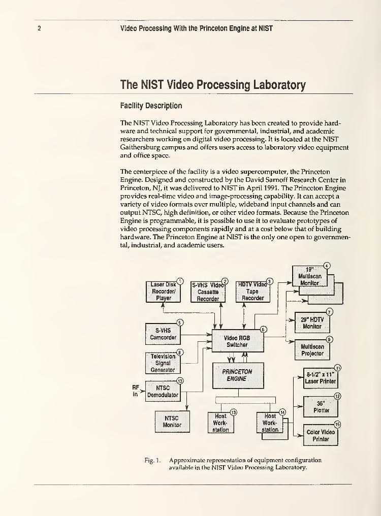
Fig. 1 . Approximate representation of equipment configuration
available in the NIST Video Processing Laboratory.

Video Processing With the Princeton Engine at NiST
The NIST Video Processing Laboratory
Supporting Equipment
The specific supporting equipment available with the Princeton Engine is
evolving, however, figure 1 describes the laboratory as it soon will be
configured. Typical operation involves connecting a video source to the
Princeton Engine through the video switcher, downloading an executable
code segment from a host workstation, and viewing or recording the pro-
cessed video output on a monitor or video recorder.
The listing below includes a more complete identification of the available
equipment. (Numbered items are keyed to the numbered circles attached to
the blocks in figure 1.) The use of specific product names does not indicate
that the item is the best available for the application nor does it constitute an
endorsement by NIST; names are shown only to clearly identify the equipn
ment in use.
1. Sony LVS-5000A, Laser Disk Processor and Recorder/Player,
with 12" monitor
2. JVC RRS600U, S-VHS Video Cassette Recorder, with 400-line resolution
3. Sony HDDIOOOPAC, HDTV Digital Processor and Recorder/Player (*)
4. Barco ICD451B, 19" Multiscan Video Monitor (3 units)
5. Panasonic AG540, S-VHS Camcorder, with character generator
6. Dynair FR-8704A, RGB Video Switcher
7. Shibasoku CM65B6, 29" HDTV Multiscan Monitor
8. Tektronix TSG 1001, Programmable Television Signal Generator
9. Sony, Multiscan Projector
10. Videotek DM141S, NTSC Demodulator11. QMS 820, 8-1/2" x 11" User Printer
12. Calcomp 58436XP, 36" Plotter (*)
13. Apollo DN400tc, Color Graphics Workstation (*)
14. Apollo DN4500, Color Graphics Workstation (2 units)
15. Shinko CHC-743MV, Color Video Printer
Not shown, but also available:
Lyon-Lamb RTC, Converter
Lyon-Lamb ENC, Encoder/Transcoder
JVC RRS600U, S-VHS Video Cassette Recorder with 19" Monitor
(*) not presently available, to be delivered

Video Processing With the Princeton Engine at NIST
The NIST Video Processing Laboratory
In addition to the equipment listed above, the workstations in the laboratory
are linked to other workstations at NIST (and to the Internet) for data trans-
fer to and from a variety of additional disk and tape storage units. Generally,
data transfer to and from the Princeton Engine is accomplished through the
high-speed video channels. But, small amounts of data can be downloadedfrom the host workstations, or captured from the Princeton Engine outputs
and saved on a host workstation, if necessary.
The Princeton Engine
General Description
The Princeton Engine was developed at David Samoff Research Center,
originally to provide television system developers with the capability of
simulating video systems in real-time. It processes a video signal one scan
line at a time, performing either an identical set of op>erations on each scan
line, or one of several sets of operations in a line-dependent manner. Field
and frame processing is accomplished by storing samples of successive scan
lines in processor memory. "Programs" resemble electronic circuit diagrams
and are developed using computer-aided-design (CAD) tools on a host
workstation. Instead of electronic components that are connected by wires,
the "circuit" consists of functional modules, representing predefined compu-tational subroutines, that are connected by data flow paths. After compila-
tion, the object code is downloaded to the Princeton Engine and run in
real-time.
The ability to make changes to the circuit diagram and re-run the modified
simulation quickly, as well as the ability to define run-time user parameters,
allows the Princeton Engine to serve as a testbed for new system/circuit
designs where the engineer can ask "what if?" and observe the results as
real-time video. The architecture and programming environment is designed
to enable the user to simulate digitally, in real-time, very complex analog and
digital video processing devices.
A simplified diagram of the architecture is shown in figure 2. The Princeton
Engine is a Single-Instruction-Multiple-Data (SIMD) massively parallel
supercomputer. That is, all the processors execute the same instruction
simultaneously but use different input data. In its present configuration at
NIST it has 1024 processors.
Video Processing Willi the Princeton Engine at NIST
The Princeton Engine
VIDEO INNTSC -RGBHDTV
rA/D INPUT SHIFT REGISTER
Hii n
PRINCETONENGINE
1024
interprcx:essorcommunication (ipc)
128 KB MEMORYPER PROCESSOR
VIDEO OUTNTSCRGBHDTV
APOLLOHOST
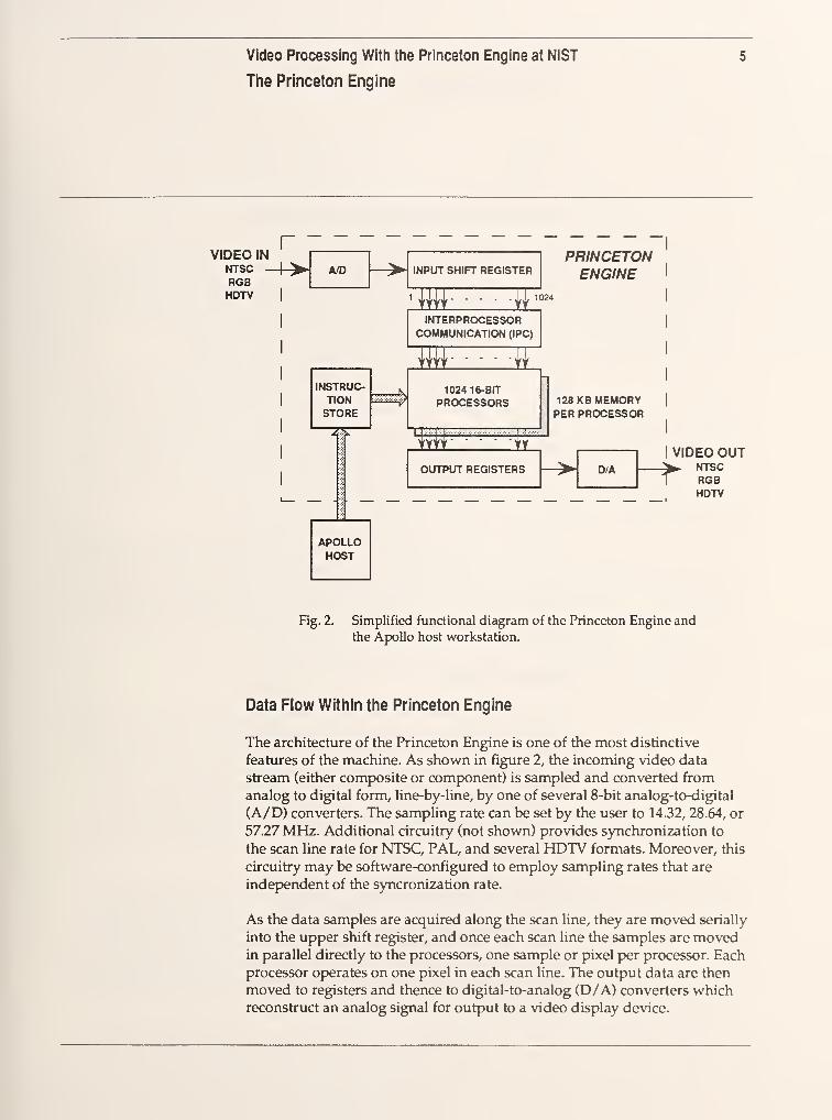
Fig. 2. Simplified functional diagram of the Princeton Engine and
the Apollo host workstation.
Data Flow Within the Princeton Engine
The architecture of the Princeton Engine is one of the most distinctive
features of the machine. As shown in figure 2, the incoming video data
stream (either compKJsite or component) is sampled and converted from
analog to digital form, line-by-line, by one of several 8-bit analog-to-digital
(A/D) converters. The sampling rate can be set by the user to 14.32, 28.64, or
57.27 MHz. Additional circuitry (not shown) provides synchronization to
the scan line rate for NTSC, PAL, and several HDTV formats. Moreover, this
circuitry may be software-configured to employ sampling rates that are
indef)endent of the syncronization rate.
As the data samples are acquired along the scan line, they are moved serially
into the upper shift register, and once each scan line the samples are movedin parallel directly to the processors, one sample or pixel per processor. Each
processor operates on one pixel in each scan line. The output data are then
moved to registers and thence to digital-to-analog (D/A) converters whichreconstruct an analog signal for output to a video display device.

Video Processing With the Princeton Engine at NIST
The Princeton Engine
instruction Flow Within the Princeton Engine
In general all of the 1024 processors of the Princeton Engine execute the sameinstruction at the same time. Thus for the purposes of programming, the
processor array may be modeled as if it were a single processor. Instructions
for all the processors are stored in a single instruction store memory, andeach instruction is sent in turn simultaneously to all processors. The instruc-
tion sequence is restarted at the beginning of each scan line.
All program development is done on the Apollo host system, including
creating (writing) and compiling programs. After being compiled on the
Apollo host, instructions (object code) are downloaded into the instruction
store memory of the Princeton Engine and executed. As mentioned above,
generally all processors execute the same instruction, however rudimentary
program branching is possible by conditionally "locking" a subset of proces-
sors, forcing them to execute null operations, while the unlocked set contin-
ues execution of the main instruction stream.
Execution of different programs on different scan lines is also possible. For
example, one program may execute during the first half of the frame or field,
and a second program during the second half providing comparison view-
ing. As, another example, one program may execute during the visible
portion of the picture and a second may operate during the vertical retrace
interval. This process is discussed in more detail in Line Dependent
Programming (LDP) below.
Real-Time Operation
In real-time op>eration, data are processed and output at the same rate as they
are input. This imposes a limit on the number of instructions for each scan
line because the processing time per scan line must not exceed the horizontal
scan period. For NTSC this real-time instruction limit is approximately 910.
For other video formats the real-time instruction limit may be calculated
from the horizontal scan rate and the processor instruction clock of nearly
14.32 mega-instructions p)er second. For an HDTV standard, 1050 lines/frame,
interlaced scan, 29.97 frames/second, the maximum number of instructions
is 455 , i.e., 14,318,182/(29.97 x 1050).
Parallelism within the processor permits up to six processor operations to
occur within one instruction. Processor operations include moving data
between registers, accessing local memory, multiplying two op>erands, and
performing arithmetic logic operations. Not all operations can be executed
together within the same clock cycle, but significant reductions in the num-ber of required instruction cycles can be achieved by efficient scheduling of
operations.

Video Processing With tiie Princeton Engine at NIST
The Princeton Engine
Non-Real-Time Operation
For those video processing algorithms that exceed the real-time instruction
limit, instructions may be included to store the incoming video data (at
incoming video rates) into local processor memory. Once sufficient data have
been accumulated (or the memory is full) processing of the stored data can
be started. When complete, the processed data (still in local memory) are
distributed to the output for reassembly into a continuous video stream for
viewing as real-time video. This mode of operation is called video-clip
processing.
The maximum length of a video clip is determined by the processor memoryand the format of the video sequence to be stored. For example, each proces-
sor has 128 Kbytes of memory organized as 64 K of 16-bit words, with
approximately 49 Kwords available for user storage. NTSC video has
525 lines per frame and a 1 /29.97 second frame rate, thus requiring
525 x 29.97 = 15,734 pixels per second per processor. Packing two pixels into
every 16-bit word, 50,176 words per processor provides up to 6.37 seconds of
NTSC video storage.
More generally, non-real-time operation is possible with either video or non-
video data. Integer arrays or fixed point real arrays may be stored in the
local processor memory subject to the limits discussed above. The indepen-
dent instruction store memory (common to all the processors) can hold up to 64
different programs each of which may be as long as 4096 instructions. By
combining multiple programs so that they execute as one, a program of up to
262,144 instructions can be executed. This permits the execution of very long
algorithms.
Advanced Features
In addition to "standard" video data flow, hardware has been included to:
- provide multiple viewable outputs on one viewing screen and /or
multiple viewing screens for side-by-side comparison of algorithms,
- execute different programs on different scan lines, for comparison of
multiple algorithms,
- transfer pixel data between processors,
- acquire portions of the output data in a capture memory for subsequent
transmission back to the Apollo host,
- route selected digital output data back to the input for further
processing.
Please refer to figure 3, a more detailed diagram of the Princeton Engine, for
the following discussion of the advanced features.

Video Processing With the Princeton Engine at NIST
The Princeton Engine - Advanced Features
14, 28, or 57 MHzi
A.
Input Clock = 28 MHz
VIDEO
INPUT
^ VIDEO
-P^ OUTPUT
Seven
-[>- 9-bit D/A
Fig. 3. Princeton Engine system diagram.
Comparison Viewing
A specialized output formatter, the Output Timing Sequence (OTS) facility,
permits split images on the output video monitor where each image is
derived from a different video signal. For example, two outputs could be
displayed, each occupying a vertical stripe of width one-half of the total
screen width. A typical use might be to compare the results of two algo-
rithms; or with three stripes to display the two results and the difference
between them. Different outputs could be assigned to different points along
a circuit diagram to observe the progression of the signal through the pro-
cessing chain. Up to four vertical stripes may be defined.

Video Processing With the Princeton Engine at NIST
The Princeton Engine - Advanced Features
In addition to using the OTS to specify the formatting of the entire picture
(i.e., a vertical stripe), several OTS patterns can be constructed and each
"mapped" to operate on certain scan lines. This "line-dependent" OTSfeature can be used to specify up to 16 OTS patterns per channel (64 total).
The screen can thus be broken into a checkerboard of video outputs.
Line-Dependent Programming
The program memory map in the microsequencer allows the user to execute
different programs during a single field or frame, as opposed to normal
operation where the same program is executed for each scan line. This
permits the user to compare the results of different programs for example byspecifying program "A" for the top half of the screen and program "B" for
the bottom half.
The advantage of line-dependent programming for comparison viewing of
multiple algorithms in real-time is particularly apparent. It is possible to
combine multiple algorithms into a single program and use OTS mapping to
select outputs from the different algorithms for comparison viewing, but in
this case the multiple algorithms must all run (sequentially) within a single
scan line period. In LDP each program is executed independently for its
particular scan line(s). Thus, (for real-time NTSC operation) each line-depen-
dent program/algorithm is limited to 910 instructions, while with OTS, the
total number of instructions for all algorithms combined must not exceed
910 instructions.
Up to 64 different programs, of up to 4096 instructions each, and a program
sequence map can be downloaded into the microsequencer to specify which
of the 64 programs is to be executed for each scan line.
Communication Between Processors
In the discussion so far, the data for each pixel on a scan line was sent to its
corresponding processor; no data sharing or transfer between processors wasattempted. However some applications will require that a processor have
knowledge of data sent to, or computed by, a neighboring processor. The
InterProcessor Communication (IPC) bus allows any data within a processor
to be sent to another processor.
To use the IPC, data generated (or received) in a processor is loaded into the
IPC bus register for that processor and an IPC bus transmit command is
executed (by all the processors) to shift all the loaded data either left or right
on the bus (multiple times if necessary) until they reach their destination

10 Video Processing With the Princeton Engine at NIST
The Princeton Engine - Advanced Features
processors. Data at each end of the bus may be looped around to the proces-
sor at the other end of the bus (to the leftmost processor for a right shift, the
rightmost processor for a left shift) or a constant user specified value may be
shifted into the ends.
Also permitted is selective transmission and reception of shifted data byprocessors. Any processor may be excluded from exporting data to the IPC
bus and/or receiving data. For example, data from every fourth processor
may be sent to the three adjacent processors to its left (or right) or every
second processor can send data to the second processor on its left, skipping
its nearest neighbor. Finally, a single processor may be selected to broadcast
to all other processors, or a subset of all other processors.
Feedback—Output-to-lnput
A 32-bit wide digital path connects the final digital output of the Princeton
Engine back to the input. This permits iterative processing of data, or com-
parison of processed data to incoming data. One possibility is to use OTS to
map the feedback path to different processors. This mapping method may be
more efficient than using multiple IPC shifts and/or broadcasts, which
require one or more processor instruction cycles per shift.
Data Capture
It is also possible to "capture" a portion of the output data stream and
upload it to the Apollo host workstation where it is stored as numerical data
in a file. The user must specify (in advance, via a mapping file) which scan
lines for which processors are to be captured. At present a maximum of 32
lines may be captured at one time.
The reverse of this process, that is, taking numerical data from the Apollo
and downloading it into the Princeton Engine for processing is accomplished
in a round about way. Directly dumping data from the Apollo to the
Princeton Engine input is not practical. The data must be loaded into specific
local processor memory locations before processing is started, and the
Princeton Engine program must be written to expect the input data in the
local processor memory rather than from the usual video source.

Video Processing With the Princeton Engine at NIST 11
Programming the Princeton Engine
Programming Philosophy
Unlike conventional computers where a program is created as lines of text,
programs for the Princeton Engine are created graphically. A "circuit dia-
gram" is drawn to represent a video processing function the user wishes to
simulate. Boxes represent modules of program code and connecting "wires"
indicate data flow paths. Figure 4 is an example of such a circuit diagram or
program. Here, a composite NTSC video signal is digitized by an analog-to-
digital converter and then fed to a delay line (HDEL.M), adders, subtracters,
dividers (DIV2.M), and filters (F1R7.M) to separate the luminance andchrominance components. Further manipulation by various modules pro-
duces the red, green, and blue video components which drive the three
digital-to-analog converters. (The synchronization and timing circuits of the
Princeton Engine cause this program to be run at the start of each scan line.)
This one circuit diagram represents the code for all 1024 processors as each
processor executes the same instruction as its neighbor, but with different
parts of the video signal as an input. This one processor model will be used
nearly universally when discussing programming. (One exception to this
model is the ability to conditionally prevent specific processors from execut-
ing instructions while normal program execution proceeds on the others, i.e.,
rudimentary branching.)
COMP VIDEO
D i
CONTRAST BRIGHTNESS
• IUSER_riWU «IUS£R_P)UU° X. " *> X,
' «
*ff))-^"^l^^-K+> Ki^ 3©^
saturatkm
»|user_pXra
RR7.M ssCx)»—3
=
M»>
TOT
*S|USER_P|W*
*rCVT-^
*..•T1NT.M^
UATnX
RED
GRE
BLU
mfjuninm
Fig. 4. A program for the Princeton Engine. This program
decodes an NTSC composite video signal into red, green,
and blue component video.

12 Video Processing Witli the Princeton Engine at NIST
Programming the Princeton Engine
Many modules have been previously coded and are available in a user
library (see Apjjendix A for a list of the available modules). When necessary,
new modules may be created by the programmer. Code within the modulesis based on the 16-bit arithmetical and logical computational abilities of the
individual processors.
All programming, creation of modules and circuit diagrams, compiling, andlinking, is done on an Apollo workstation and only the final machine code is
downloaded to the Princeton Engine for execution. Although the Engine is a
single user machine, multiple users may share its use by developing pro-
grams simultaneously on the Apollo workstations and running their code in
turn. Video monitors are provided alongside all Apollo workstations for
viewing the video outputs.
More traditional text-based compilers are under development, and may in
the future augment or partially replace the programming tools available
today. These compilers are discussed in the "Future Programming Lan-
guages" subsection on page 24. However, to appreciate the role these compil-
ers will play in program development we suggest you read the "Program-
ming Examples" section (below) first.
Programming Examples
The programming environment for the Princeton Engine is unusual in that it
is based on a computer-aided-design tool—the Mentor Graphics CADsystem for circuit diagram construction. This has the advantage of being a
familiar environment for many electronics engineers, but computer scientists
and other programmers may need to translate their traditional techniques to
this new method.
As implied by the discussion in a previous sub-section, two levels of pro-
gramming are available for the Princeton Engine. "High level" programmingis the construction of the circuit diagram. In many cases all the necessary
modules for the circuit have already been created and construction of the
circuit diagram is all that is required. However, if some specialized modules
are not available, "low level" assembly language programming will be
required for creation of the modules. The two examples that follow illustrate
these two programming processes.
Video Processing Witli the Princeton Engine at NIST
Programming the Princeton Engine
13
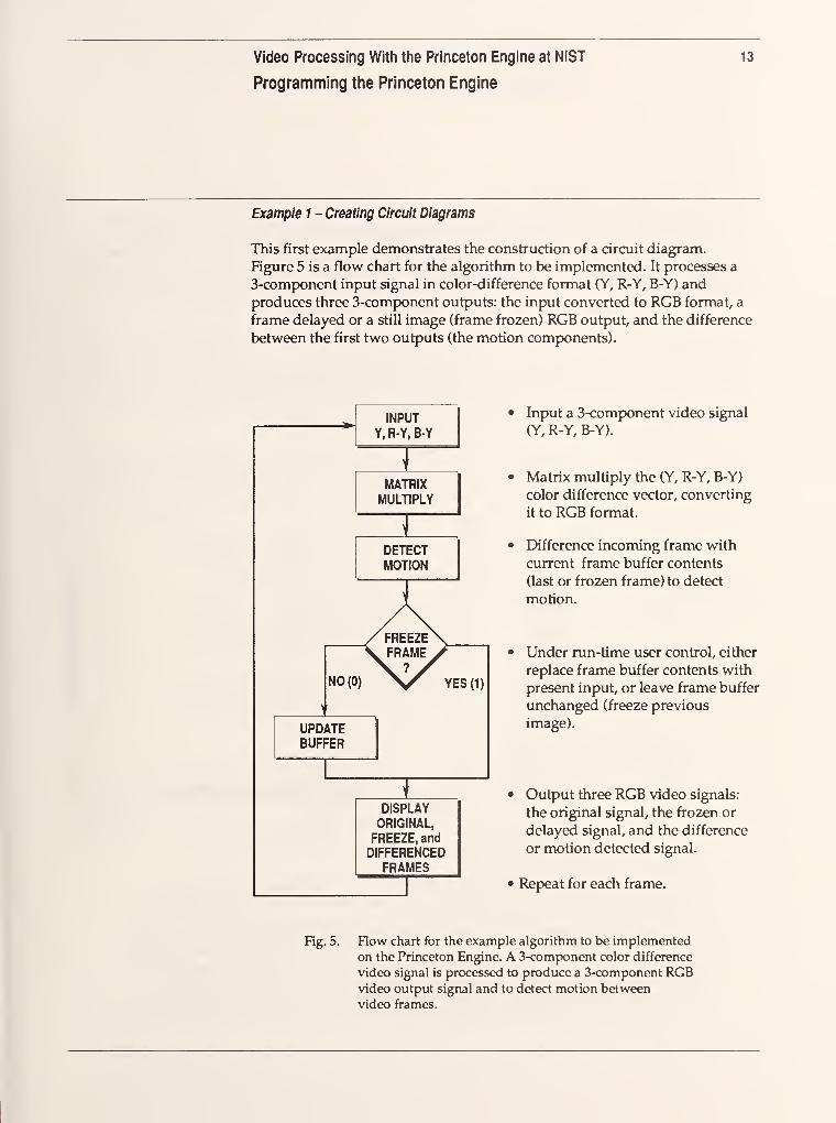
Example 1 - Creating Circuit Diagrams
This first example demonstrates the construction of a circuit diagram.
Figure 5 is a flow chart for the algorithm to be implemented. It processes a
3-component input signal in color-difference format (Y, R-Y, B-Y) and
produces three 3-component outputs: the input converted to RGB format, a
frame delayed or a still image (frame frozen) RGB output, and the difference
between the first two outputs (the motion components).
INPUT
Y, R-Y, B-Y
NO(0)
UPDATEBUFFER
MATRIXMULTIPLY
DETECTMOTION
YES(1)
DISPLAY
ORIGINAL,
FREEZE, and
DIFFERENCEDFRAMES
Input a 3-component video signal
(Y, R-Y, B-Y).
Matrix multiply the (Y, R-Y, B-Y)
color difference vector, converting
it to RGB format.
Difference incoming frame with
current frame buffer contents
(last or frozen frame) to detect
motion.
Under run-time user control, either
replace frame buffer contents with
present input, or leave frame buffer
unchanged (freeze previous
image).
Output three RGB video signals:
the original signal, the frozen or
delayed signal, and the difference
or motion detected signal.
Repeat for each frame.
Fig. 5. Row chart for the example algorithm to be implemented
on the Princeton Engine. A 3-component color difference
video signal is processed to produce a 3-component RGBvideo output signal and to detect motion between
video frames.
14 Video Processing With the Princeton Engine at NIST
Programming the Princeton Engine
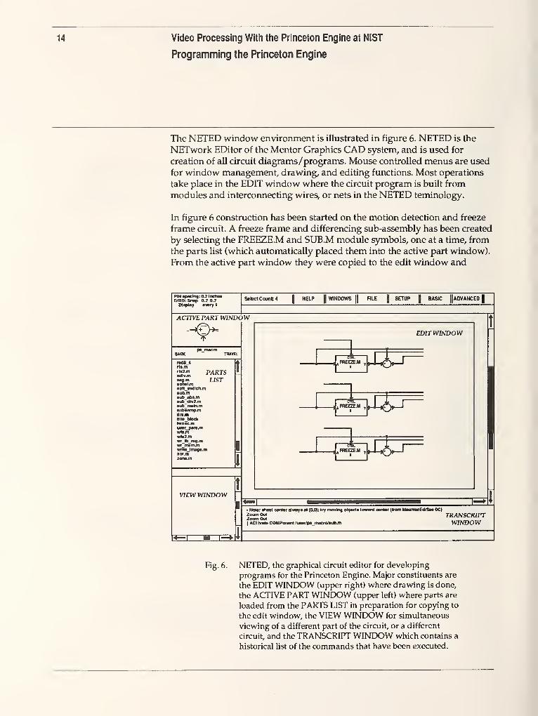
The NETED window environment is illustrated in figure 6. NETED is the
NETwork EDitor of the Mentor Graphics CAD system, and is used for
creation of all circuit diagrams/programs. Mouse controlled menus are used
for window management, drawing, and editing functions. Most operations
take place in the EDIT window where the circuit program is built from
modules and interconnecting wires, or nets in the ISTETED teminology.
In figure 6 construction has been started on the motion detection and freeze
frame circuit. A freeze frame and differencing sub-assembly has been created
by selecting the FREEZE.M and SUB.M module symbols, one at a time, from
the parts list (which automatically placed them into the active part window).
From the active part window they were copied to the edit window and
PIN •pKlng: 0.2 InchMGRID: Snap 0.2 0.2
Dtiplay awry 1
Select Count 4 | HELP | WINDOWS||
RLE | SETUP | BASIC ADVANCED
ACTIVE PART WINDOW
•ofasl.r
•oft_*vfltch.m
ftutLmsub_abt.msit)_fflv2.mMAmatn.m•ub*afnp.mtlnl.mtlito_b*f>cfc
lwo*c.muOTr_jtari.mwte.mwt«2.mwr_t)_r»g.mwr mom.mwrftfl_l(nBg«jnlor.mzona.m
PARTSUST
VlEy<jyJINDOVJ
EDIT WINDOW
^ rir~p
-mrJ^d^
Hi ^.«,j_,(5^
- Noi*: ihMl ofitor alaaya M (0.0): tiy moving oli|«1s toward center (Iroin ktoafNMEdfSoo OC)Zoom oijt TRANSCRIPTZoom Out[ ACrivaw COMPonMH fUMr/p*_macra/nibjn WINDOW
Fig. 6. NETED, the graphical circuit editor for developing
programs for the Princeton Engine. Major constituents are
the EDIT WINDOW (upper right) where drawing is done,
the ACTIVE PART WINDOW (upper left) where parts are
loaded from the PARTS LIST in preparation for copying to
the edit window, the VIEW WINDOW for simultaneous
viewing of a different part of the circuit, or a different
circuit, and the TRANSCRIPT WINDOW which contains a
historical list of the commands that have been executed.

Video Processing With the Princeton Engine at NIST
Programming the Princeton Engine
15
placed in their desired locations. Interconnecting nets were then routed
between the module pins. Finally, the subassembly was copied twice to
produce the complete drawing shown in the figure. (As an example of the
capabilities of the drawing program, note that the standard SUB.M module,
shown in the active part window, has been flippjed about its horizontal axis
before being placed in its final position in the edit window.)
The circuit is completed by copying the necessary remaining modules into
the edit window and drawing connecting nets. When the final wiring is
complete, the design "syntax" is checked for disconnected or misconnected
nets and if no errors are obtained the design is saved to disk. After construc-
tion with NETED, the design must be compiled and linked using the Graphi-
cal Program Comp>oser (GPC). The resulting machine code may then be
downloaded and run on the Princeton Engine.
R-Y
B-Y
ADC MO PROBE 1
HOOCrBI.
FREO = 14HHZ
ADC M1
VOOE^W.FREa = 1«HZ
ADC M2
MOOEsBl.FHEa = 1«IHZ
MATRIX
i RGB.M
6
•*
vm.—
FREEZE.M ky-T
TOT.FREEZE.M ky-f
-, FREEZE.M L^yJ
RED8 4
SCALE =1XOTt MAP RLE = m.0T9i
GRE6 4
9CALE:1IOTI lAP FILE^UXOTai
BLUB 4
SCALE r 11
OTS lAP RLE=UX.OTSa
RED
GREEN
BLUE
Fig. 7. The complete example circuit converts color-difference
video signals to RGB. The circuit displays four outputs (as
indicated by the 4 input signals to each DAC), the original
video input, a frame delayed or a still image video signal,
the difference between the delayed or still image signal
and the original signal, and a probe output. The probe
input can be temporarily attached to any net (wire) in the
circuit for viewing the signal along that segment. (For this
example the probe input has been attached to the output of
ADCMO as indicated by the PROBEl label; routing wires
are not used to indicate probe input cormections.)
16 Video Processing With the Princeton Engine at NIST
Programming the Princeton Engine
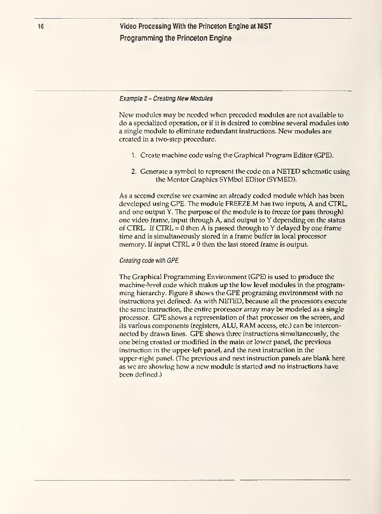
Example 2 - Creating New Modules
New modules may be needed when preceded modules are not available to
do a specialized operation, or if it is desired to combine several modules into
a single module to eliminate redundant instructions. New modules are
created in a two-step procedure.
1. Create machine code using the Graphical Program Editor (GPE).
2. Generate a symbol to represent the code on a NETED schematic using
the Mentor Graphics SYMbol EDitor (SYMED).
As a second exercise we examine an already coded module which has been
develof>ed using GPE. The module FREEZE.M has two inputs, A and CTRL,and one output Y. The purpose of the module is to freeze (or pass through)
one video frame, input through A, and output to Y depjending on the status
of CTRL. If CTRL - then A is passed through to Y delayed by one frame
time and is simultaneously stored in a frame buffer in local processor
memory. If input CTRL ^ then the last stored frame is output.
Creating code with GPE
The Graphical Programming Environment (GPE) is used to produce the
machine-level code which makes up the low level modules in the program-
ming hierarchy. Figure 8 shows the GPE programing environment with no
instructions yet defined. As with NETED, because all the processors execute
the same instruction, the entire processor array may be modeled as a single
processor. GPE shows a representation of that processor on the screen, and
its various components (registers, ALU, RAM access, etc.) can be intercon-
nected by drawn lines. GPE shows three instructions simultaneously, the
one being created or modified in the main or lower panel, the previous
instruction in the upper-left panel, and the next instruction in the
upper-right panel. (The previous and next instruction panels are blank here
as we are showing how a new module is started and no instructions have
been defined.)

Video Processing With the Princeton Engine at NiST
Programming the Princeton Engine
17
Processor resources available to the programmer include:
- a 64-register register file (REG_FILE) for temporary storage,
- access to the interprocessor communication bus for shifting data to
neighboring processors (LEFT, IPC_BUF, RIGHT, COM_REG),- a 2-input arithmetic-logic unit (ALU) for arithmetic and logic
operations,
- a 2-input multiplier (MPY, PP, and P) for multiplication and product bit
extraction,
- access to RAM for local data storage and module input and output, and- the use of intermediate registers IREGl, IREG2, Dll for access to
the register file (REG_FILE) and intermediate register DI for
access to RAM.
Operations generally consist of moving data to and from the ALU or multi-
plier and the intermediate registers. To improve code readability, the regis-
ters may be labeled by the user to indicate their contents.
[ D9RC - PflMCETON ENGME GfUPHCAl. PROCRAUUNG EDITQn - VERSKM 2.0 i
on1
REC-1
>>i_*Dn pj>on
poim
HEQI MEGI
£
VTI*)1
PP
>nm1
CUn BtVT: 1 EMCwnnwuPvrf EOT UOOe. STNCMlOMOUt
piCKPftooam nwCHcm.
Fig. 8. Graphical Programming Editor showing the PE processor
model and pop-up menu controls for selecting processor
operations.

18 Video Processing With tlie Princeton Engine at NIST
Programming the Princeton Engine
We will now briefly discuss the GPE program instructions for the FREEZE.Mexample. Figure 9 shows the first instruction of the program listing of the
FREEZE.M module as produced by GPE. (The seven additional instructions
for the module continue on the next several pages.) Data flow between
registers is indicated by lines with arrowheads which are drawn between the
source and destination register. We recommend that labels be assigned to the
registers to indicate their contents. For example, note that the register indi-
cated as IREGl in figure 8 (its real name) is labeled in figure 9 below, as it
will contain zero after execution of the instruction. Not all registers can be
directly interconnected, hardware restrictions prohibit connecting the
register labeled LCM to accumulator ACCl, for example. Pop-up menus(not shown) are used to select ALU operations. A complete listing of all
processor operations is included in Appendix B.
LEFT IPC BUF RIGHT COM_REG
CUP OFF
INPUT_PIN(aRL)
ALU(A)
\> )
ALU(B) /
MPY(A)
PP
MPY(B)
ACCl
INST1
Fig. 9. The first GPE instruction for the FREEZE.M module.
(Seven additional instructions continue on the next 4 pages.)
Instruction 1: Communication between modules is accomplished by storing
output data in a defined location in local processor memory where the next
module will be instructed to look for it. The program compiler (Graphical
Program Composer, GPC) resolves these memory location definitions
between modules; the programmer assigns an input or output to the appro-
priate pin name on the module symbol. For our example, input to the
module is obtained through the input pins A, and CTRL. In instruction 1
input CTRL is loaded from RAM into the RAM-intermediate-register, here
labeled "CTRL" to remind us of its contents. At the same time registers 54
and 33 of the register file are loaded into PORTl and PORT2 intermediate
registers labeled "0" and "LCM." Registers 54 and 33 contain predefined
values of zero, and the current scan line number, LCM, respectively.
Video Processing With the Princeton Engine at NIST
Programming the Princeton Engine
19
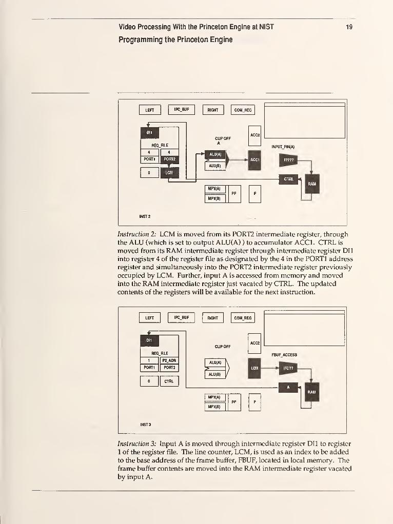
Instruction 2: LCM is moved from its PORT2 intermediate register, through
the ALU (which is set to output ALU(A) ) to accumulator ACCl. CTRL is
moved from its RAM intermediate register through intermediate register DIl
into register 4 of the register file as designated by the 4 in the PORTl address
register and simultaneously into the PORT2 intermediate register previously
occupied by LCM. Further, input A is accessed from memory and movedinto the RAM intermediate register just vacated by CTRL. The updated
contents of the registers will be available for the next instruction.
LER IPC_BUF RIGHT COM_REG
1 (
REG_HLE
ACC2uururr
FBUF ACCESS
1 P2_ADRALU(A)
>V B 1
PORTl P0RT2
/ Q-—^H7mALU(B)
pjp_~nCTRL H
MPY(A)
pp P
MPY(B)
NST3
Instruction 3: Input A is moved through intermediate register DIl to register
1 of the register file. The line counter, LCM, is used as an index to be addedto the base address of the frame buffer, FBUF, located in local memory. Theframe buffer contents are moved into the RAM intermediate register vacated
by input A.
20 Video Processing Witli tiie Princeton Engine at NIST
Programming the Princeton Engine
LEFT IPC_BUF WOHT COM_REG
Oil
CUP OFFA+B
ACC2
'J P2_ADRI—JIJiUHv
LCM RA^^jiIH P0RT2 .JmS ;—*^j]]j|y^^E^KEIH
1 A(F)1
RAM1 1
MPY(A)
pp P
MPY(B)
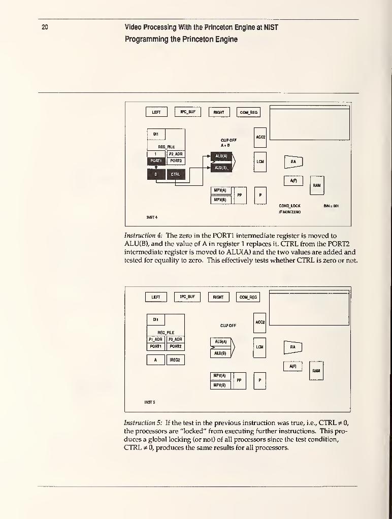
INST 4
COND_LOCK
IF NONZERO
BIN = 001
Instruction 4: The zero in the PORTl intermediate register is moved to
ALU(B), and the value of A in register 1 replaces it. CTRL from the PORT2intermediate register is moved to ALU{A) and the two values are added andtested for equality to zero. This effectively tests whether CTRL is zero or not.
1
LEFT IPC_BUF RIGHT COM_REG
DI1
CUP OFFACC2
Dl C
P1_ADR P2_ADRALU(A)
)LCM RAPORTl P0RT2 >
ALU(B)
A IREG21 .. 1
RAM1^ '
1
MPY(A)
PP P
HPY(B)
irJST5
Instruction 5: If the test in the previous instruction was true, i.e., CTRL ^ 0,
the processors are "locked" from executing further instructions. This pro-
duces a global locking (or not) of all processors since the test condition,
CTRL ^ 0, produces the same results for all processors.

Video Processing With the Princeton Engine at NIST
Programming the Princeton Engine
21
LOT IPC_BUF BGHT COM_REG
OtlAcca
REG..RLE FBUF ACCESS
P1_ADR P2_ADRALU(A)
> V 1.PORTI P0RT2
/ Q- •'W^^ 1
ALU(B) 'VI IREG2 V^^m^t 1
^^>1 MW 1
MPY(A)
pp p fMPY(B)
NST6
Instruction 6: This instruction is only executed if the processors were not
locked in the previous instruction. If the processors are locked, this instruc-
tion will effectively be replaced by a no-operation. The current value of input
A is stored in the frame buffer at index LCM overwriting the existing
contents.
otl
REG .RLE
P1_ADR P2_ADR
PORTI P0RT2
A IREG2
INST 7
CUP OFF
ALU(A)
\> >
ALU(B) /
MPY(A)
PP
MPY(8)
LCM[HI]
RAH
GLOBAL UNLOCK
Instruction 7: Globally, unconditionally, unlock all processors.

22 Video Processing With the Princeton Engine at NIST
Programming the Princeton Engine
LER IPC BUF RIGHT
ni
REG.HLE
P1_ADR P2_ADR
P0RT1 P0RT2
CUP OFF
IREG1 IREG2
ALU(A)
\> )
ALU(B) /
MPY(A)
PP
MPY(B)
COM_REG
ACC2
ACC1
OUTPUT_PIN<Y)
irCTS
Instruction 8: Move the old value of A obtained from the frame buffer, and
previously stored in the RAM intermediate register, to output pin Y.
Note that if CTRL ^ 0, then globally locking the processors prevents the
frame buffer from being updated in instruction 6, thus the value of A that
will be obtained from the frame buffer during the next cycle (in instruction 3)
will be the last stored value, thus freezing the picture.
Generating a symbol
Symbol generation is done using the Mentor Graphics SYMED program.
Generation is simplified however by the use of a symbol generation macro
that interrogates the user about the number of input and output pins, their
names, and their locations, and then draws an appropriate symbol part. The
symbol (figure 10) is also labeled with the number of instructions in the
module (8). In most cases this is all that is required. For specialized symbols,
all the tools of the SYMED program are available to customize the size,
shape, and other features of the symbol.
OUT
Fig. 10. NETED symbol for FREEZE.M module.

Video Processing With the Princeton Engine at NIST
Programming the Princeton Engine
23
Controlling/Debugging a Running Program
Control of the Princeton Engine is accomplished by sending specialized
conimands (SPES commands) from the Apollo workstations. These 43
predefined SPES commands control all aspects of Princeton Engine opera-
tion, including loading programs, setting input and output configurations,
changing program variables while the program is running, initializing or
loading data into local processor memory, and capturing output data.
Although the user can t)^ the commands directly, two methods have been
developed to make the system easier to use. A graphical control environ-
ment (GCE) program can be run on the Apollo to provide an interface
between the user and the SPES commands, or NETED can be placed in a
GCE mode to provide control over some operations.
The GCE display is shown in figure 11 with the applications menu pulled
down. This configurable menu allows the user to execute a series of SPEScommands (previously defined in a text file) to set the Princeton Engine
environment and download an application in one operation. User param-
eters defined in the downloaded program will show in the boxes to the left.
The present value of the parameter is shown in the box immediately below
the parameter name, and the value is changed by clicking on the up or downarrows. Additional menus at the top of the display allow the user to conve-
niently execute some of the more common SPES commands.
PE Graphical Control Environment. [Version 1.1] (C)f' '^
EXIT ][^ COMMANDS ][ PE_TOOLS ][ MENTOR
i.m tcimoHt
NTSC_DECODE
FHEEZE_FRAME
FRAME_LINE_COMB
QBERT
SOBErFILTER
COLOR_EDGE_DETECT
QUANTIZER
PSEUDO_COLOR
ZONE_PLATE^GEN
FIELD_PRO_SCAN
LDP_DEMO
MY_APPLICATION_1
MY APPLICATION 2
Fig. 11 Graphical Control Environment display with controls for
modifying user parameters contrast, brightness, saturation,
and tint of the BASIC_NTSC program shown in Fig. 4.

24 Video Processing With the Princeton Engine at NIST
Programming the Princeton Engine
When NETED is used to control the Princeton Engine, it is placed in the GCEmode. Drawing operations are suspended, but revised menus are madeaccessible for downloading the program displayed in the NETED edit
window, controlling the input and output registers, and changing user
parameters and filter coefficients. The most important feature, however, is
the ability to attach a moveable probe to different parts of the circuit and"view" the data at that point. To do this the outputs of up to 3 probes may be
assigned to DAC inputs, and the actual probe-input position in the circuit is
then assigned (or changed) at run time. (See figure 7 for an example of a
circuit diagram with a probe.) Probing is one of the more jxjwerful methods
for debugging circuits.
Future Programming Languages
A C-compiler and a FORTRAN compiler are presently under development at
the David Samoff Research Center. Although both compilers will be cross-
compilers, i.e., they run on the Apollo workstations and produce code for the
Princeton Engine, their functions will not be interchangeable.
At the present time the Graphical Program Editor (CPE) is the only tool
available for developing assembly code for a module for the Princeton
Engine. The Princeton Engine C-compiler (PEC) will implement a subset of
the C language and eventually can replace GPE in the code development
process. It is important to note that the PEC produces code for a module
which then must be linked to other modules using a higher level program-
ming environment such as NETED; one cannot develop a complete program
using the initial release of the PEC. Initial testing of the C-compiler suggests
that the code which it produces is nearly as efficient as hand-optimized code
produced using GPE, moreover, program control functions such as "loops"
may be used only via PEC. Delivery of the compiler is expected in the near
future.
Alternatively, the Princeton Engine FORTRAN 90 compiler (which will
implement a subset of FORTRAN 90) will be a substitute for NETED for the
construction of a complete program. Preliminary results suggest that there
will be a high overhead associated with the FORTRAN compiler.

Video Processing With the Princeton Engine at NIST 25
The NIST Training Program
NIST will provide training in the use of the Princeton Engine for DARPAcontractors and users from other collaborating organizations. This includes
training for:
- the Apollo/Aegis operating system,
- Mentor Graphics CAPTURE schematic drawing software,
- using previously constructed library modules,- construction of user-programmed modules,- and using Princeton Engine-specific run-time operating software.
The more advanced features of the Princeton Engine (line-dependent pro-
gramming, OTS mapping, and line-dependent OTS) will not normally be
included in the training because they will not be needed by most users, are
relatively complex, and require a thorough knowledge of the Princeton
Engine hardware. (See the section on The Princeton Engine - Advanced Features
for further detail about these topics.) Instead, NIST personnel will assist the
user directly, providing specific solutions for the user's problem if the use of
such advanced capabilities becomes necessary.
The training program consists primarily of self-directed study using refer-
ence material and workbook exercises provided by NIST. NIST experts will
be on hand to answer questions or to explain difficult concepts. Sufficient
student time will be made available on tiie Apollo workstations and the
Princeton Engine for running and testing the workbook exercises or other
problems the student may wish to try.
The training program is expected to take from 1 to 2 weeks to complete,
depending on previous experience the student may have with the Aegis
operating system or the Mentor Graphics CAD software. At the end of the
program the student should have basic compjetency in developing programs
for the Princeton Engine and running and debugging those programs.
NIST Contacts
For more information about the NIST laboratory or the Princeton Engine at
NIST contact:
Dr. Bruce F. Field
(301) 975-4230, email: [email protected]
or
Dr. Charles Fenimore
(301) 975-2428, email: [email protected]
National Institute of Standards and Technology
B344, Metrology Building
Gaithersburg, MD 20899


Video Processing With tlie Princeton Engine at NIST 27
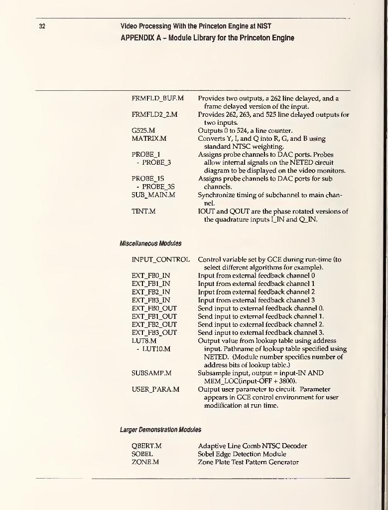
APPENDIX A
Module Library for the Princeton Engine
There are presently over 150 modules in the Princeton Engine Library. These
nnodules are general purpose code elements that form the basis for develop-
ing Princeton Engine "programs" using the NETED circuit diagrammingsoftware. (See Programming the Princeton Engine for more detail about
NETED). A list of the modules is presented below, categorized bymodule function.
Analog-to-Digital Conversion Modules (video input)
Several modules have been created to represent and control the analog-
to-digital (ADC) hardware inputs. They convert an input analog video
signal to a digital stream for processing by other modules. The output is
represented in either two's-complement or binary format depending onthe module used. Different A/D modules are also used to represent one
of three main or three subchannels.
main channel #0, two's-complement
main channel #0, binary format
main channel #1, two's-complement
main channel #2, two's-complement
sub channel #0, two's-complement
sub channel #1, two's-complement
sub channel #2, two's-complement
ADC MO 8-bit ADCADC MOB 8-bit ADCADC Ml 8-bit ADCADC M2 8-bit ADCADC SO 8-bit ADCADC SI 8-bit ADCADC S2 8-bit ADC
Digital-to-Analog Conversion Modules (video output)
These modules are used to route the processed digital video signal from
other modules to the output digital-to-analog (DAC) converters. Somemodules include additional digital inputs (up to four) that are routed to
additional OTS registers so that the separate video signals may be
displayed in vertical strijDes on the same monitor. (See T/ie Princeton
Engine, Advanced Features for additional information about OTS channel
outputs.) All modules are two's-complement.
RED8 1 8-bit DACREDS 2 8-bit DACRED8 4 8-bit DACGRE8 1 8-bit DACGRE8 2 8-bit DACGRE8 4 8-bit DACBLU8 1 8-bit DACBLU8 2 8-bit DACBLU8 4 8-bit DACDAC3.8 1 8-bit DACDAC3.8 2 8-bit DAC
single-input red DAC2-input red DAC4-input red DACsingle-input green DAC2-input green DAC4-input green DACsingle-input blue DAC2-input blue DAC4-input blue DACsingle-input DAC#32-input DAC#3

28 Video Processing With the Princeton Engine at NIST
APPENDIX A - Module Library for the Princeton Engine
DAC3.8_4DAC4.8_1DAC4.8_2DAC4.8_4DAC5.8_1DAC5.8_2DAC5.8_4DAC6.8_1DAC6.8_2DAC6.8 4
8-bit DAC8-bit DAC8-bit DAC8-bit DAC8-bit DAC8-bit DAC8-bit DAC8-bit DAC8-bit DAC8-bit DAC
4-input DAC#3single-input DAC#42-input DAC#44-input DAC#4single-input DAC#52-input DAC#54-input DAC#5single-input DAC#62-input DAC#64-input DAC#6
Logical/Arithmetic Modules
These modules perform the indicated computation on one or more 16-bit
two's complement inputs and produce a 16-bit output. Inputs are
typically denoted by A, B, ... etc. (Exceptions are noted.)
ABS.M lAI
ADD.M A + BADD3.M A + B + CADD DIV2.M (A + B)/2AND.M Bitwise logical 'AND' of A and BCLIP.M Clip input-A to lie within inputs LOL and UPL.
COMP.M Output 1 if input-A >= input-TH, if A < TH.
CONST.M Constant (user specified on NETED).
D1V2.M A / 2^ (N = 2 to 7).
- DIV128.MINV.M Binary NOT( A
)
LTl.M A limited to N bits (N = 1 to 9).
-LT9.MMEDIAN3.M Median of three inputs. A, B, CMIN.M Minimum of two inputs. A, B
MAX.M Maximum of two inputs. A, BMAX3.M Maximum of N inputs (N = 3 to 7).
- MAX7.MMIXER.M A X K + B X ( 1-K ) (A, B, and K are inputs, K is an
8-bit input,0<K<l).MULT.M (A X B) / 2«
MULT2.M A X 2^ (N = 2 to 7).
- MULT128.MONESC.M one's complement(A)
OR.M Bitwise logical 'OR' of A and B
PROC_NUM.M Processor number {- to 1023).
QUANT8.M A quantized to 8 bits.
SDIV.M Two outputs, Q = INT( A/B );

Video Processing With tiie Princeton Engine at NIST
APPENDIX A - Module Library for the Princeton Engine
29
SEG.M
SUB.MSUB_DIV2.MTWOSC.MXOR.M
If (input-A is between two inputs ST and END)then output = input-MAXelse output = input-MIN
A-B(A-B)/2two's complement(A) (A is one's complement).
Bitwise logical exclusive 'OR' of A and B
Control Structures
Branching and looping are presently supported only by forcing selected
processors to execute NOPs (no operations) while other processors
continue to execute the instruction stream.
BRANCH_TEST.M Branch test module is an example of this condi-
tional execution.
MUX2.M
MUX4.M
SOPT SWITCH.M
2-input multiplexer, one of two inputs selected
based on third input CNTL = or 1.
4-input multiplexer, one of four inputs selected
based on third input CNTL = 0, 1, 2, or 3.
Effective dissolve between 2 inputs A and B.
Four inputs and one table are required. A, B are
video inputs K, and TH are control inputs, and
table Tl is the dissolve mapping function.
Control of Interprocessor Communication Operations
BC1.M-BC5.M
BP.M
CLEAR IPC.M
IPC_LS.M- IPC_LS3.M
IPC_RS.M- IPC RS3.M
Input broadcast to other processors according to
broadcast pattern BCl. Modules provide from
one to five wait instructions.
Configures the IPC circuitry to bypass processors
according to a pattern defined at compile time.
Clear Interprocessor Communication circuitry
erasing any previously loaded broadcast or
bypass pattern.
Interprocessor left shift N times. (N = 1 to 3).
Interprocessor right shift N times. (N = 1 to 3).

30 Video Processing With the Princeton Engine at NiST
APPENDIX A - Module Library for the Princeton Engine
Filters
A number of finite impulse response filters for spatial and temporal
filtering are included. Initial values for the filter coefficients are specified
while creating the circuit using NETED but they may be updated later
during run-time.
FIRXX_YY.M is a generic two-dimensional filter with the following
naming convention:
XX - the horizontal filter length, and
YY = the vertical (temporal) filter length.
The internal accuracy of these filters is limited to 8 bits.
nR00_03.M, nR00_05.M, nR00_07.M, nR00_{)9.M,
nR03_00.M, nR03_03.M, nR03_05.M, nR05_00.M,nR05_05.M, nR07_00.M, nR07_07.M, nR09_00.M,nR09 09.M
nR3.M, nR7.M,nR9.M
nR16 39 OO.M
Horizontal 8-bit filters with 3, 7, and 9 taps
respectively.
A two-dimensional 16-bit accuracy filter, horizon-
tal filter length = 39, vertical filter length = 0.
Delay Modules and Local Processor Memory Operations
FRAME_BUF.M
FRAME_BUF2.M
FREEZE.M
FREEZE2.M
HDEL.MHDELOl.M
- HDEL07.M
RD MEM.M
Output is frame delayed version of input. The
frame time is defined by the video input format.
Two outputs are frame delayed versions of inputs
A and B. (Frame size is defined by the video
input format.)
Output frame delayed version of input-A if input-
CTRL = 0, if CTRL = 1 output previously stored
frame.
Output frame delayed versions of inputs A and B
if input-CTRL = 0, if CTRL = 1 output previ-
ously stored frame.
Input delayed by one scan line.
Each module produces multiple outputs (YOl ...
YON, N = 1 to 7), delayed versions of input by Nscan lines.
MEM_LOC(3800 + input-OFF)
Read (and output) a memory location in local
processor memory specified by address
input-OFF (relative to 3800 HEX)

Video Processing With the Princeton Engine at NIST
APPENDIX A - Module Library for the Princeton Engine
31
RD_FB_REG.M Read a memory location in local processor
memory specified by a compile time address.
Address also provided to output R_AD.RD_IFRAME_STORE.M Read input-A into frame buffer specified by
input-ST_R.
READ_IMAGE.M Output data from frame buffer sp)ecified by input-
ST_ADRS.Output data for global (to all modules) frame
buffer specified by input-ST_R.
Two simultaneous outputs from double global
frame buffer specified by input-STR.
Write input data to global frame buffer specified
by input-ST_R.
Write input data to double global frame buffer
specified by input-ST_R.
Output data from local processor memory from
address specified by input-R_AD. Write input-A
to a memory location R_AD.MEM_LOC(3800 + input-OFF)
Write input to a memory location in local
processor memory specified by address input-
OFF (relative to 3800 HEX).
RFS.M
RFS2.M
WFS.M
WFS2.M
WR FB REG.M
WR MEM.M
Video Controls and A/TSC Specific Modules
BRCT.M
CBS AT.M
CTBR.MDEMOD.M
DEMOD_SUB.MFCOMB.M
FLD262.M
FLD DELAY.M
FLD_SWITCH.MFRAME COUNT.M
Modify video input by brightness and contrast
values.
Given Y and C inputs, apply brightness, contrast,
and saturation values, and separate into RGBcomponents.
Modify input by contrast and brightness values.
Chroma demodulator separates the NTSC chroma
(C) signal into two components (1 and Q).
Chroma demodulator for the sub channel.
Separates composite NTSC signal into luminance
output and chrominance output using a frame
comb.
Output F262 is input A delayed by 262 horizontal
scan lines.
Outputs D262, D263, and D264 are input Adelayed by 262, 263, and 264 horizontal scan
lines respectively.
If NTSC field is even then output=0 else output=l
.
(Dutputs a count that increments on the first line of
every NTSC frame (every 525 lines).
32 Video Processing With the Princeton Engine at NIST
APPENDIX A - Module Library for the Princeton Engine
FRMFLD_BUF.M
FRMFLD2_2.M
G525.MMATRIX.M
PROBE_l- PR0BE_3
PROBE_lS- PR0BE_3S
SUB_MAIN.M
TINT.M
Provides two outputs, a 262 line delayed, and a
frame delayed version of the input.
Provides 262, 263, and 525 line delayed outputs for
two inputs.
Outputs to 524, a line counter.
Converts Y, I, and Q into R, G, and B using
standard NTSC weighting.
Assigns probe channels to DAC ports. Probes
allow internal signals on the NETED circuit
diagram to be displayed on the video monitors.
Assigns probe channels to DAC p>orts for sub
channels.
Synchronize timing of subchannel to main chan-
nel.
lOUT and QOUT are the phase rotated versions of
the quadrature inputs I_IN and Q_IN.
Miscellaneous Modules
INPUT_CONTROL
EXT_FBO_INEXT_FB1_INEXT_FB2_INEXT_FB3_INEXT_FB0_OUTEXT_FBl_OUTEXT_FB2_OUTEXT_FB3_OUTLUT8.M
- LUT10.M
SUBSAMP.M
USER PARA.M
Control variable set by GCE during run-time (to
select different algorithms for example).
Input from external feedback channel
Input from external feedback channel 1
Input from external feedback channel 2
Input from external feedback channel 3
Send input to external feedback channel 0.
Send input to external feedback channel 1.
Send input to external feedback channel 2.
Send input to external feedback channel 3.
Output value from lookup table using address
input. Pathname of lookup table specified using
NETED. (Module number specifies number of
address bits of lookup table.)
Subsample input, output = input-IN ANDMEM_LOC(input-OFF + 3800).
Output user parameter to circuit. Parameter
appears in GCE control environment for user
modification at run time.
Larger Demonstration Modules
QBERT.MSOBELZONE.M
Adaptive Line Comb NTSC Decoder
Sobel Edge Detection ModuleZone Plate Test Pattern Generator

Video Processing With tiie Princeton Engine at NIST
APPENDIX B
33
Processor Operations
Processor operations consist of moving data between the intermediate
registers, the arithmetic logic unit (inputs ALU(A) and ALU(B)), the multi-
plier (inputs MPY(A) and MPY(B)), and the interprocessor conununication
bus (IPC_BUF).
The ALU performs arithmetic, logical, and functional operations on 16-bit
data with its output routed to one or both of the output accumulators, ACClor ACC2 dep>ending on the operation.
The multiplier operates on two 16-bit two's complement inputs routed to
MPY(A) and MPY(B) producing a 32-bit intermediate value. The Product
Picker (PP) allows the user to select 16 contiguous bits of the 32-bit product
for placement into the output register P. The product picker effectively
provides division by powers of 2 and can facilitate fixed point arithmetic.
The figure below is a representation of the processor.
The interprocessor communication bus is used to transfer data between
processors. Within a processor, data is routed to the IPC_BUF register before
the transfer and the data received from a second processor is routed from the
IPC_BUF register after the transfer is complete. The LEFT and RIGHT boxes
on the diagram serve to initiate shifting operations. More complicated
transfer patterns are invoked using the COM_REG.
LEFT IPC BUF RIGHT C0lyl_REG
DI1
REG.RLE
P1_ADR P2_ADR
PORTI P0RT2
CUP OFF
IREGI IREG2
ALU(A)\> )
ALU(B) /
MPY(A)
PP
MPY(B)
ACCl [^RAM
GPE processor model which includes an ALU, hardware Multi-
plier, 64-register register file, RAM access, and IPC access.

34 Video Processing Witfi the Princeton Engine at NIST
APPENDIX B - Processor Operations
ALU Operations
CLIP ON
CUP OFFA + B
A + B + C
A-BB-AA-B + C
B-A + C
A + B + 1
CON[A - B]
A ORBAANDBAXORBABS(A)AB
ISC(A)
2SC(A)
MAX(A, B)
MIN(A, B)
ST_DIVCONT_DrVEND_DIVPACK
Prevents overflow by limiting ALU output to 7FFF
or 8000 HEX.No overflow correction is performed.
Add inputs A and B.
Add inputs A and B with carry from previous
operation.
Subtract B from A.
Subtract A from B.
Subtract B from A with borrow from previous
operation.
Subtract A from B with borrow from previous
operation.
Add inputs A, B, and 1.
Conditional subtract. If (A - B) > result is A - B,
otherwise result is A.
Bitwise logical OR of A and B.
Bitwise logical AND of A and B.
Bitwise logical XOR of A and B.
Absolute value of input A.
Route ALU input A through ALU to ACCl.Route ALU input B through ALU to ACC2.Convert two's complement to one's complement.
Convert one's complement to two's complement.
Maximum of A and B.
Minimum of A and B.
Start software divide of A/B.
Continue software di\'ide (one instruction p>erbit).
End software divide with quotient and remainder.
Pack lower 8 bits of A and B into 16-bit result.
Video Processing With the Princeton Engine at NIST 35
APPENDIX C- Technical Paper
The Princeton Engine: A Real-Time Video System Simulator
D. Chin
J. Passe
R Bernard
H.Taylor
S. Knight
©IEEE. Reprinted with permission from
IEEE TRANSACTIONS ON CONSUMER ELECTRONICS
Vol 34, No. 2, pp. 285-297, May 1988
NOTE: A few technical details in "The Princeton Engine: A Real-Time Video
System Simulator" may disagree with material presented in the body of this
technical note. This is a result of upgrades and improvements made to the
Princeton Engine after publication of the paper. In the event of a disagree-
ment it is generally safe to assume that the information in the body of the
technical note is correct.


Chin, et al.: The Princeton Engine: A Real-Time Video System Simulator 28S
THE PRINCETON ENGINE: A REALTIME VIDEO SYSTEM SIMULATOR
D. Chin, J. Passe, F. Bernard, H. Taylor, 8. Knight
David Sarnoff Research Center
CN 5300, Princeton, NJ 08543-5300
(609) 734-2301 TELEX: (609) 734-2221
Abstract
The Princeton Engine is a 29.3 GIPS image processing
system capable of simulating video rate signals - includ-
ing NTSC and HDTV video - in real-time. It consists of a
massively-parallel arrangement of up to 2048 processing
elements. Each processing element contains a 16-bit
arithmetic unit, multiplier, a 64-w/ord triple-port register
stack (one write, two read), and 16,000 words of local
processor memory. In addition, an interprocessor commu-
nication bus (IPC) permits exchanges of data between
neighboring processors during one instruction cycle. Wefurther describe a new method of parallel programming
for DSP applications and provide several examples.
^ItrQdilSdQQ
The design of an NTSC digital television has required
extensive computer simulations to verify digital signal
processing algorithms. High-level language programs
have been used to simulate a few fields of the target
video system [1, 2]. New signal formats such as Ad-
vanced Compatible TV(ACTV) [3] also require
significant manpower and
simulation time to obtain
acceptable results. While
these simulations are im-
portant to the design pro-
cess, they provide limited
intormation about the per-
formance of the actual
system under real-time
conditions. This has result-
ed in a costly development
cycle in which hardware
prototypes are built for
each of several genera-
tions of experimental sys-
tems.
Processor
mic steps per pixel. If each pixel is clocked at 14MHz
(70ns cycle) rate, a single processor would have to be
able to execute one algorithmic step every 20 picosec-
onds to sustain real-time operation. This is about two or-
ders of magnitude greater than the next generation of
supercomputers.[4] In addition to the intensive computa-
tional requirements, a real-time video simulation system
must be able to continuously sustain I/O at 14MHz or
better.
Numerous attempts have been made at applying super-
computer or multiple processor architectures to image
processing and real-time video simulation problems. Fig-
ure 1 compares the different approaches in terms of pro-
cessor topology - how they are mapped onto an array of
pixels. The first approach ( "A" in Figure 1) employs a
single, very high performance computational node or sev-
eral nodes such as a Cray X-MP. In the Connection Ma-
chine [5] system, 64,000 sequential single bit processors
operate in a Single Instruction Multiple Data (SIMD)
mode. Pixel data is mapped in a processor per pixel
mode, as shown in "B" in Figure 1 , for the entire array of
pixels. This method is
also referred to as fine
grain parallel process-
ing, wherein many sim-
ple processors are used
to simultaneously per-
form the same compu-
tation on a large array
of data [6].
An alternative to fine
grain architectures for
a multiple processor
system is the course
grained approach in
which considerably few-
er processors of great-
LEGENDA-SUPEHCOMPUTER
B - PFOCESSCW PER PIXEL (SYSTOLC)
C - DISTTRBUTED PnOCESSOR ARRAYFOR M X N PIXELS
D - ONE PROCESSOR PER COLUMN
The problem of performing true, real-time video simula-
tions can be characterized in the following terms: the al-
gorithms necessary to implement an advanced, motion
adaptive, NTSC decoder requires about 1400 algorith-
Figure 1.
To Pixel Mapping Schemes.
er computational power are employed. One such system
from NHK [7], uses standard bit-slice processors as pro-
cessing elements. Up to eight 16-bit processing units run-
ning at 7.16MHz and connected unidirectionally have been
implemented in this system. Each processor contains a
replication of a full frame of image data in memory, elim-
Contributed Paper
Manuscript received March 17, 1988.
0098 3063/88/0200 0285$01.00 © 1988 IEEE
286 IEEE Transactions on Consumer Electronics, Vol. 34, No. 2, MAY 1988
inating memory access contention. As shown in ap-
proach "C" in Figure 1 , each processor executes the al-
gorithm for a specific region of pixels in the image plane.
This system has been used for real-time frame syn-
chronizing and mixing.
Another mapping of processor topology to an array of
pixels is the Scan Line Array of Processors approach,
or SLAP [8]. In this system, a linear array of identical
processors are connected in a nearest neighbor fashion
and are operated in an SIMD mode (as shown in "D" of
Figure 1). Each processor contains an integer arithmetic
unit, register file and a single stage of a shift register.
As an image scan line is loaded into the array, each pro-
cessor latches one pixel. Algorithm ex-
ecution proceeds with processors in
parallel. A 512 processor SLAP imple-
mentation with a 250ns instruction cy-
cle time can perform about 125 real
time instructions for each pixel of a
512x512 image. A more recent imple-
mentation of SLAP will yield about
500 instructions [9]; however, extend-
ed instructions, such as multiply, will
take as many as ten instructions.
Thus, real-time simulations of large
video systems are not possible.
eo is performed in a processor per column architecture,
similar to the SLAP system (see "D" in Figure 1). The
processors are tightly coupled by a communication net-
work which supports nearest neighbor exchanges of
data in a single cycle and random exchanges between
any two processors in a 64 processor boundary in one
cycle. A local memory with sufficient storage for 32
frames of video data makes it possible to implement
both temporal and vertical algorithms.
System Operation Overview
The initial application for the Princeton Engine will be in
performing real-time video simulations of NTSC and
ONE CYUNDEn Of COLUMN
UU.TPIE
drKXar G ,
*" B ,
'••pwy G ,
'^'B,
SOURCESELECmON
DISPLAY
INTERFACE
^
•CLOCK GEN,
4.INE LOCKED-BURST LOCKED
Several architectures have been pro-
posed which combine features of both
coarse and fine grain processing. Onesuch architecture is the Warp Comput-
er, a linear systolic array of proces-
sor cells [1 1]. Each processor cell con-
tains a 32-bit multiplier and ALU unit
capable of sustaining 10 Mflops. I/O
between processor cells occurs at
20MHz, and the combination of high, single processor per-
formance and I/O bandwidth are claimed to make both
fine and coarse grain processing possible. However, real-
time video and image processing simulations are greatly
limited by a small number of processing cells (see "B" in
Figure 1) and the need to interface an I/O frame store
buffer. Temporal processing across multiple fields is lim-
ited by a mapping scheme where each processor cell
must act as a fine grain processing element for a large
number of pixels.
The Princeton Engine combines features of both coarse
and fine grain processing architectures. It is implemented
from a large number (up to 2048) of high speed (14
MHz), single cycle, 16-bit processors. Processing of vid-
• TEST SIGNALGEhEHATON
^ PRINCETON ENGINF(N - 010 fw NTSC)
INPUT SHIFT REGISTERH Sag—
ijuiiiINTHRPROCeSSOfla»*A
NStagnwLINEAR ARRAY
of
N-PARALLELPROCESSORS
with
NX 16X 16K
LOCAL MEIuCIRIES
||' MULTIIMULTIPORT RAM OUTPUT Si
HOSTCOMVIER
I/O
CO^fTROL
Ouvul Coniral 2^
. NPV/T / OUTRJT TUNG
Figure 2. Princeton Engine System Overview
ACTV video systems. In the Princeton Engine system,
digitized video is continuously shifted into the input shift
register (top of Figure 2). After a line of video is com-
pletely loaded into the registers, the video is transferred
in parallel to the interprocessor communication (IPC)
buffers. The processor can then fetch the data and op-
erate on it locally or globally. After all pixels are pro-
cessed, they are downloaded to the output section within
a line time. In this way, continuous video can be produced
at the output. The processing should be completed in less
than a line time to achieve real-time simulation. For four
times subcarrier sampled NTSC data, the maximum
number of instructions for real-time simulation, Np^ , is:

Chin, et al.: The Princeton Engine: A Real-Time Video System Simulator 287
input parallel load period ^ 910x70ng ^ g^g instructions
instruction period 70ns
for a 910 processor system. This is the total number of
instructions available to accomplish the 1400 algorithmic
steps required to implement the example NTSC system.
In the Princeton Engine, each processor micro-instruction
can typically achieve three algorithmic steps yielding a
total capability of 2730 algorithmic steps. By doubling
the number of processors to 1820, Np^ , is:
2 X 910 x70ns = 1820 instructions,
70ns
for a total of 5460 algorithmic steps.
The Princeton Engine achieves a linear speedup in the
number of instructions which can be executed while still
maintaining real-time operation. Likewise, this same
speedup can be realized by halving the instruction period.
Engine Controller Input and Output
All system program control, video input and output is
contained in the controller. A Video Input section which
allows source signal selection and
data conversion (A/D and D/A
converter) is shown at left in Fig-
ure 2. Up to 48 total bits of video
input source with three indepen-
dent clocks can be processed (six
8 bit sources, three 16-bit sourc-
es, etc). A multibus interface be-
tween the host computer and the
controller permits program and
control code to be downloaded.
Within the controller, there is a
16,000 instruction memory (word
length is 89 bits). The controller
transfers instructions from this
program memory by sending a
stream of identical instructions
to each of the processing ele-
ments in the array. Video data is
transferred in parallel to the ar-
ray of processors - one line of
video at a time - each processor
receiving a single sample. Theoverall transfer rate of the input
Figure 3.
video data is 1 .3 Gbit/second (48 x 28.64MHz). The con-
troller also includes a video output timing and display
section. In this section, a stream of pixels, 64 bits wide
(i.e. eigiii 8 bit channels, four 16-bit channels, etc.), is
transferred from the array of processors back to the
output and display section at 1.8 Gbit/second (64 x
28.64MHz). The arrangement of pixels at output is com-pletely programmable via the Output Timing Sequencebus (OTS) within the Graphical Control Environment
(GCE) and occurs in parallel with instruction execution.
TTie Processing Element
The engine core consists of an array of up to 2048 pro-
cessing elements. Figure 3 shows a block diagram of the
processing element. Each element has a 16-bit ALU, a16-bit Multiplier, a 64-word triple-port register stack and
a 16-bit address/data external memory interface. In ad-
dition, processing elements are connected at the chip lev-
el via a 16-bit programmable data bus (IPC), which sup-
ports rapid exchanges of data between processors. Afull compliment of processors can realize a throughput of
29.3 GIPS (2048 X 14.32MHz).
The processing element also contains special hardware
support for maintaining lookup tables in external memo-ry. External addressing can be of either an absolute, an
indirect or a table index type. During each instruction cy-
IB (IMD Fd)
All butMS aro 16 brts witk
url«s5 otherwiw noted
IMD ; Irrmxlals Oiti
NND : Non Normal DiU
Processing Element Block Diagram.
cle memory addresses can be directly encoded into the
immediate field of the instruction. Next, the address can
be generated indirectly from a register or the accumula-
tor; finally, the address can be formed by combining a

288 IEEE Transactions on Consumer Electronics, Vol. 34, No. 2, MAY 1988
register value with immediate data to form
a table index. In table index mode, 8 MSBbits of immediate data provide a bit maskindex. This mask determines which bits of
the lower eight bits form the table address.
Memory access is completed in one cycle.
The immediate field of any instruction can
also be used to load a data constant into
the ALU, Multiplier or on-chip memory stack.
BROADCAST
e-BBroadcasting
Processor
APPLICATION : adaptive filtering . histograms
BYPASS
Total throughput of the system is signifi-
cantly increased by the incorporation of mul-
tiple internal data paths within the process-
ing element. This permits a high degree of
secondary parallelism in program operation.
For example, in filter operations, a pixel can
be shifted left, while simultaneously, an
ALU operation, a multiply operation, and an
external memory access are being per-
formed. The use of secondary parallelism in this way
results in at least a 3:1 reduction in the number of in-
structions when compared to the number required on a
conventional microprocessor.
Interprocessor Ccnfimunication Bus
The Interprocessor Communication Bus (IPC) provides
high speed exchanges of data between processing ele-
ments and the video input/output processing logic. IPC
bus operations can be of a broadcast type (one proces-
sor to many) or of a bypass type (where there are ran-
dom length non-overlapping bidirectional connections be-
tween processors). A new IPC bus topology for the
entire engine can be generated in two instructions. Figure
4 illustrates these two communication schemes and their
applications.
-» II
I
-n~
APPLICATION
Bypassed^
Processors
fault tolerance ; TREE S HISTOGRAM CALCULATIONS
Figure 4. Broadcast and Bypass IPC Modes.
Once a bypass pattern is set, communication is bidirec-
tional - e.g. left and right I/O operations send correspond-
ing data n processors up or down stream, according to
the bypass pattern configuration. Connections within a
64-processor boundary will require only one instruction,
while a worst case bypass pattern will require five in-
structions. During exchanges which require more than
one instruction, processors can continue to perform all
other ALU, Multiplier, internal register and external
memory operations.
This communication topology is the key to implementing
horizontal filtering algorithms. And, because of the large
local memory and register stack sizes, vertical and tem-
poral filter operations can be efficiently performed, as
well. Figures 5 and 6 illustrate possible vertical and tem-
poral operations using local memory to store data for
in the Broadcast mode (top of Figure 4), one
processor is designated as the sender and as
many of the other processors as are required
by the algorithm can be designated as receiv-
ers. Data transfer is accomplished in one in-
struction to any of the processors within the
transmitter's 64-processor boundary. In the
worst case (assuming 2048 total processors),
it would take five instructions from any one
processor to all others.
Bypassing operates in a similar manner, ex-
cept multiple processors can be connected in
any pattern, provided no two paths cross.
LINEAR -VERTICAL
Pn.i P
01-» I III
^^^. • m VI •
I« V ^
l::i m:I
I
'
APPI ICATIQN :
VERTICAL FW FLTERS.NEAREST NEIGHBOR CALCULATIONS
Figure 5. Vertical Filter Operations.
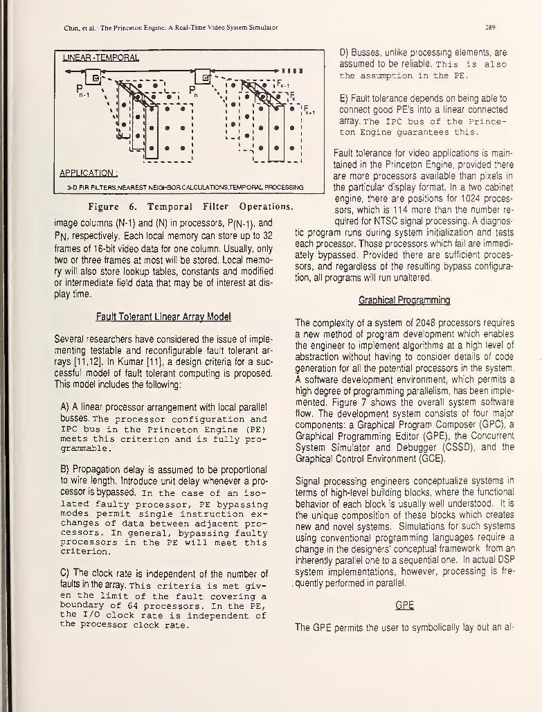
Chin, et al.: The Princeton Engine: A Real-Time \'ideo System Simulator 289
LINEAR -TEMPORAL
n^n-1
Bf --*-» 1 1 1
1
APPLICATION :
3-D FIR FILTERS,NEAREST NEISHBOR CALCUUVT10NS,TEMP0RAL PROCESSING
Figure 6. Temporal Filter Operations,
image columns (N-1) and (N) in processors, P(N-1). and
Pn, respectively. Each local memory can store up to 32
frames of 16-bit video data for one column. Usually, only
two or three frames at most will be stored. Local memo-
ry will also store lookup tables, constants and modified
or intermediate field data that may be of interest at dis-
play time.
Fault Tolerant Linear Array Model
Several researchers have considered the issue of imple-
menting testable and reconfigurable fault tolerant ar-
rays [11,12]. In Kumar [11], a design criteria for a suc-
cessful model of fault tolerant computing is proposed.
This model includes the following:
A) A linear processor arrangement with local parallel
busses. The processor configuration andIPC bus in the Princeton Engine (PE)meets this criterion and is fully pro-grammable.
B) Propagation delay is assumed to be proportional
to wire length. Introduce unit delay whenever a pro-
cessor is bypassed. In the case of an iso-lated faulty processor, PE bypassingmodes permit single instruction ex-changes of data between adjacent pro-cessors. In general, bypassing faultyprocessors in the PE will meet thiscriterion.
C) The clock rate is independent of the number of
faults in the array. This criteria is met giv-en the limit of the fault covering aboundary of 64 processors. In the PE,the I/O clock rate is independent ofthe processor clock rate.
D) Busses, unlike processing elements, are
assumed to be reliable. This is alsothe assuinption in the PE.
E) Fault tolerance depends on being able to
connect good PE's into a linear connected
array. The IPC bus of the Prince-ton Engine guarantees this.
Fault tolerance for video applications is main-
tained in the Pnnceton Engine, provided there
are more processors available than pixels in
the particular display format. In a two cabinet
engine, there are positions for 1024 proces-
sors, which is 114 more than the number re-
quired for NTSC signal processing. A diagnos-
tic program runs during system initialization and tests
each processor. Those processors which fail are immedi-
ately bypassed. Provided there are sufficient proces-
sors, and regardless of the resulting bypass configura-
tion, all programs will run unaltered.
Graphical Programming
The complexity of a system of 2048 processors requires
a new method of program development which enables
the engineer to implement algorithms at a high level of
abstraction without having to consider details of code
generation for all the potential processors in the system.
A software development environment, which permits a
high degree of programming parallelism, has been imple-
mented. Figure 7 shows the overall system software
flow. The development system consists of four major
components: a Graphical Program Composer (GPC), a
Graphical Programming Editor (GPE), the Concurrent
System Simulator and Debugger (CSSD), and the
Graphical Control Environment (GCE).
Signal processing engineers conceptualize systems in
terms of high-level building blocks, where the functional
behavior of each block is usually well understood. It is
the unique composition of these blocks which creates
new and novel systems. Simulations for such systems
using conventional programming languages require a
change in the designers' conceptual framework from an
inherently parallel one to a sequential one. In actual DSP
system implementations, however, processing is fre-
. quently performed in parallel.
The GPE permits the user to symbolically lay out an al-
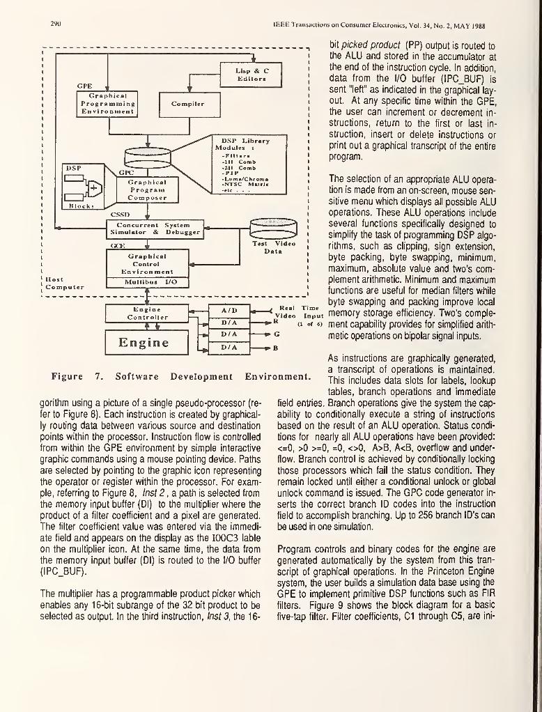
290 IEEE Transactions on Consumer Electronics, Vol. 34, No. 2, MAY 1988
GPEGraphical
Progra mmingEnvironment
Lisp & CEditors
Compiler
DSP
15Klock!
GPCGraphicalProgramComposer
CSSD
DSP LibraryModules :
-Flltcra111 Comb211 Comb-PI P• Luma/Cltroma-NTSC Matrix-tic . . .
ConcurrentSimulator &
SystemDebugger
OCE
HostComputer
GraphicalControl
En vi ron mentMultibus I/O
Test VideoData
EngineController
TTEngine
A/D
D/A
D/A
D/A
bit picked product (PP) output is routed to
the ALU and stored in the accumulator at
the end of the instruction cycle. In addition,
data from the I/O buffer (IPC_BUF) is
sent "left" as indicated in the graphical lay-
out. At any specific time within the GPE,the user can increment or decrement in-
structions, return to the first or last in-
struction, insert or delete instructions or
print out a graphical transcript of the entire
program.
The selection of an appropriate ALU opera-
tion is made from an on-screen, mouse sen-
sitive menu which displays all possible ALUoperations. These ALU operations include
several functions specifically designed to
simplify the task of programming DSP algo-
rithms, such as clipping, sign extension,
byte packing, byte swapping, minimum,
maximum, absolute value and two's com-
plement arithmetic. Minimum and maximumfunctions are useful for median filters while
byte swapping and packing improve local
memory storage efficiency. Two's comple-
(1 of 6) ment capability provides for simplified arith-
metic operations on bipolar signal inputs.
• Real TimeVideo Input
,R
Figure 7. Software Development Environment
gorithm using a picture of a single pseudo-processor (re-
fer to Figure 8). Each instruction is created by graphical-
ly routing data between various source and destination
points within the processor. Instruction flow is controlled
from within the GPE environment by simple interactive
graphic commands using a mouse pointing device. Paths
are selected by pointing to the graphic icon representing
the operator or register within the processor. For exam-
ple, referring to Figure 8, Inst 2 , a path is selected from
the memory input buffer (Dl) to the multiplier where the
product of a filter coefficient and a pixel are generated.
The filter coefficient value was entered via the immedi-
ate field and appears on the display as the I(X)C3 lable
on the multiplier icon. At the same time, the data from
the memory input buffer (Dl) is routed to the I/O buffer
(IPC_BUF).
The multiplier has a programmable product picker which
enables any 16-bit subrange of the 32 bit product to be
selected as output. In the third instruction, Inst 3, the 16-
As instructions are graphically generated,
a transcript of operations is maintained.
This includes data slots for labels, lookup
tables, branch operations and immediate
field entries. Branch operations give the system the cap-
ability to conditionally execute a string of instructions
based on the result of an ALU operation. Status condi-
tions for nearly all ALU operations have been provided:
<=0, >0 >=0, =0, <>0, A>B, A<B, overflow and under-
flow. Branch control is achieved by conditionally locking
those processors which fail the status condition. They
remain locked until either a conditional unlock or global
unlock command is issued. The GPC code generator in-
serts the correct branch ID codes into the instruction
field to accomplish branching. Up to 256 branch ID's can
be used in one simulation.
Program controls and binary codes for the engine are
generated automatically by the system from this tran-
script of graphical operations. In the Princeton Engine
system, the user builds a simulation data base using the
GPE to implement primitive DSP functions such as FIR
filters. Figure 9 shows the block diagram for a basic
five-tap filter. Filter coefficients, CI through C5, are ini-
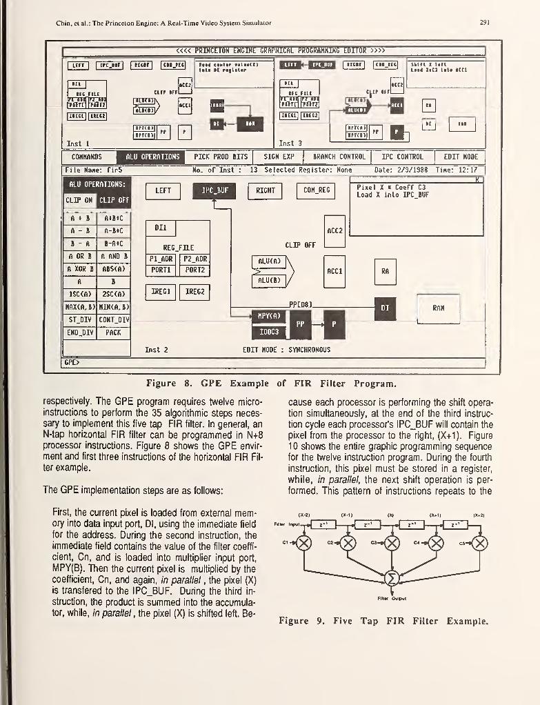
Chin, et al.: The Princeton Engine: A Real-Time Video System Simulator 291
«« PRWCET6H mw mmthi mtJ^MM mm »»
IitFT
I I
irc_iiFI I
iitirI I
cii.itcl
lEC FILErrjiif]rrjnjitrr fStn
taU l[ r«|ltt«r
IICCl IIEC2
Inst 1
30ttj(t)\
lEC FILE
rsiJi TStn
SktFt I ItftL*a4 IiC3 tat* ICCl
|ItECl||HEC?|
Inst 3
COHHANDS ftLU OPERnnONS PICK PROD BnS SICH EXP BRANCH CONTROL IPC CONTROL EDIT MODE
File Na«e: fir5 No. of Inst : 13 Selected Register: None Date: 2/9/1988 Tine: 12:17
ALU OPERATIONS:
CLIP ON CLIP OFF
LEFT RIGHT CON REG
A t B
B - A
A OR fi
A XOR B
ISC(A)
HAX(A,B)
ST DIV
END DIV
A*B*C
A-BtC
B-A*C
A AND B
ABS(A)
2SC(A)
HIN(A,B)
CONT DIV
PACK
DIl
REG..FILE
P1_ADR P2_ADR
PORTl P0RT2
IREGl IREG2
CLIP OFF
ACC2
Pixel X « Coeff C3Load X into IPC BUF
K
ALU(A)
ALU(B)
ACCl RA
.PPIOST.
-mmRAN
Inst 2 EDIT MODE : SYNCHRONOUS
CPE>
Figure 8. GPE Example of FIR Filter Program.
respectively. The GPE program requires twelve micro-
instructions to perform the 35 algorithmic steps neces-
sary to implement this five tap FIR filter. In general, an
N-tap horizontal FIR filter can be programmed in N+8processor instructions. Figure 8 shows the GPE envir-
ment and first three instructions of the horizontal FIR Fil-
ter example.
The GPE implementation steps are as follows:
First, the current pixel is loaded from external mem-ory into data input port, Dl, using the immediate field
for the address. During the second instruction, the
immediate field contains the value of the filter coeffi-
cient, Cn, and is loaded into multiplier input port,
MPY(B). Then the current pixel is multiplied by the
coefficient, Cn, and again, in parallel , the pixel (X)
is transfered to the IPC_BUF. During the third in-
struction, the product is summed into the accumula-
tor, while, in parallel , the pixel (X) is shifted left. Be-
cause each processor is performing the shift opera-
tion simultaneously, at the end of the third instruc-
tion cycle each processor's IPC_BUF will contain the
pixel from the processor to the right, (X+1). Figure
10 shows the entire graphic programming sequence
for the twelve instruction program. During the fourth
instruction, this pixel must be stored in a register,
while, in parallel, the next shift operation is per-
formed. This pattern of instructions repeats to the
(X-2) (X-1)
Flltor Inpi
Flllac OufKjl
Figure 9. Five Tap FIR Filter Example.

292 IEEE Transactions on Consumer Electronics. Vol. 34. No. 2, MAY 1988
^LEFT 1 ! IPt.llFl
{iicir 1 ciijE({
j
Itti Clilirlitt II ri|
lllllCI)titir
LEFT IIJIIH j IIEi: 1 CIIJE! riiii I ctiff aLltd I lit! Ift_HF
1 11l«Ct2| [
riTP iff! i
IICC2HI! 1
Ill 1
lEt FILE 1lEt rilE '
ff?
CLIf IFF
U71 iffFJ Hi
IlLlCI)/1
rFi uTtj hi |4LIU>\
lILICDt/ICClnV\' iMlrj'
-fiiIlECi: IIEC2; lltECl IIEC:' — '"
!
Inst 2
nn
DiirT(i)" 1] 1
mSJL^i*Inst 1
iicir , cii lEc;I
Skirt i lift=
' L>l< llC3 lit! icci
I lEt FILE\
i>atn Mir;;
illEEi; illECZ;
Inst 3
CLIP iff' i
s k >wwi
—
trimw Hg
ft[TP,
|^^«—^^23 '' '"'^'ciijEi Skm I lift
im (I>1) liti IIEC2
ESTlEC FILE
irECl 1^3
fTUTTTTK
Unci),'licet : 11
Inst ^
ifFd)j I 1 B
1 -^————
—
{lECIF CII.IEC| Lll4 (ItUi
Ltl< (I>2>:< uti r
lilt iie;2;licir cii_iE( iiiiw ciitir fiiiici)
^ i
1ICC2
CI If iffI
ICCIIil iTt ptdicti
1^1 '"-—
—
' III: !
' LlK Clt2)iC5 lltl P
"i
II
lEt FILE CLIP IFF.
|LI(ii\1> > liCCl
iLi(i)/;
[111
PI lEC Pc III „
iiEii ^22 IT-
-yg^" M -^ii«"^ l!,!^iJ
-cnn/ inIII
rill ffW f ...I — '-^ ! "
Inst 5
"SlEHI imalil~lBIns I S
LEFT il.'ll.i—JlM'lI 1 CII.IEt' SklC. I rljlil^^^^^^ ^^^^ .... icciiMliti inriictllitl ICCl
LEF- aij* ! i»—fHI ! CII IE! Skid (I-l) rl)kl^^^^ ^^^ LIK tI-1) lltl IIEtZ
i Hii
ICC2 kllM |1CC2
1 rit FILE S4'.'"^ tr. FUf ti-iF iff;
V-"rp;_i» —icnQi. —'^^^^^-^ —St)—'i '
"MM MM Tornx, i— ;—
,
piiri rrm -s ^n i.m it.
-nnrcSa ^'^^' ^
1 tr [ Ml^^
In 1 lU'"">:,»
' !_, '1
liprcDi: ' !"!;ip>av: :
•
Inst 7
llfKIV " '
Inst 8
—^^^—^^—
^
]
lltIT I ' CII_tEt: , Llll (I-l)lC2 1 ti p
HEC2LEFT i ' IPC.IIFJ 1 1 ICir ' CM lEC Icciiiliti irKictt
lltl ICClLll^ (I-2)iCl lltl P
i
I.CC2! IICC2
n TP IFF' lEt FILE
IIIi
' IE; FILErrrp iff! i
[iLKlbK '
>
—
:) '"1:
"1 ILKI)/
Pinri"nlr}:1^
r-
—
*t[_mcr UjjJ
i
^ HiiiEiiirTTn 1
^iir \ ,T
'
til ^[111
111
Inst 9!
1KQ2lJll~lflInsl 10
1
LEFTI I
IPC IIF1
I IKirI
I CII lECl I Icciiiliti llll pridict1,-1i^j^ j^^j
Inst 11
IIECl||IIEtT]I
^^I
I
1ftII III
LEFT, 1 IPCJIF IltIT iCIIIEt ; LiH (11 tir litllt'
''
''
'
= '
tl III
IE; FILE
Ttrrr
IIECli :IIEC2
Inst 12
^ Mn S—
I
l:j
Figure 10. GPE Program for Five Tap FIR Filter.
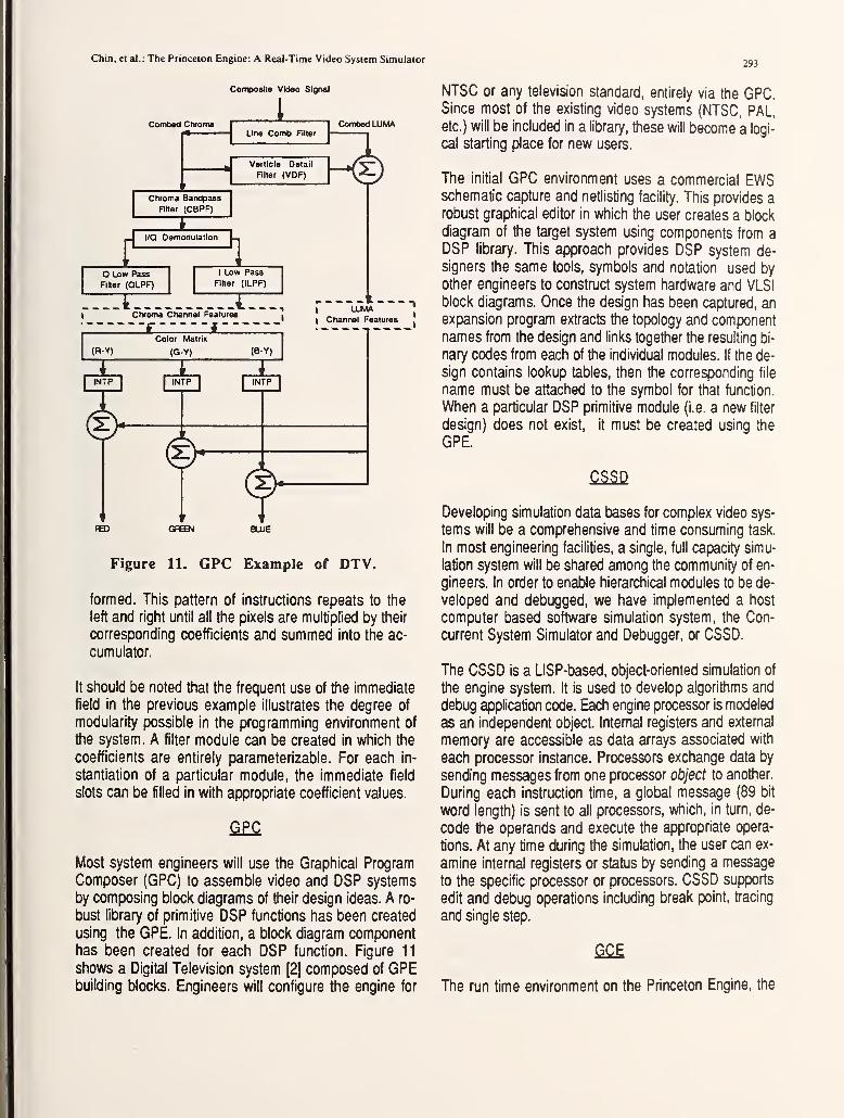
Chin, et al.: The Princeton Engine: A Real-Time Video System Simulator
Composite Video Signal
Combed ChromaLine Comb Filter
Vertlcle Detail
niter (VOF)
Combed LUr
Chroma BarxJpass
RIter (CBPF)
£l/Q Demodulation |_
J'
Q Low Pass
Fitter (OLPF)
I Low Pass
niter (ILPF)
Chroma Channel Features
~~f f
\ LUMA\ Channel Features
(R-Y)
Color Matrix
(G-Y)
INTP
i-
(B-Y)
IEINTP
faxiE
Figure 11. GPC Example of DTV.
formed. This pattern of instructions repeats to the
left and right until all the pixels are multiplied by their
corresponding coefficients and summed into the ac-
cumulator.
It should be noted that the frequent use of the immediate
field in the previous example illustrates the degree of
modularity possible in the programming environment of
the system. A filter module can be created in which the
coefficients are entirely parameterizable. For each in-
stantiation of a particular module, the immediate field
slots can be filled in with appropriate coefficient values.
Most system engineers will use the Graphical Program
Composer (GPC) to assemble video and DSP systems
by composing block diagrams of their design ideas. A ro-
bust library of primitive DSP functions has been created
using the GPE. In addition, a block diagram component
has been created for each DSP function. Figure 11
shows a Digital Television system [2] composed of GPEbuilding blocks. Engineers will configure the engine for
293
NTSC or any television standard, entirely via the GPC.Since most of the existing video systems (NTSC, PAL,
etc.) will be included in a library, these will become a logi-
cal starting place for new users.
The initial GPC environment uses a commercial EWSschematic capture and netlisting facility. This provides a
robust graphical editor in which the user creates a block
diagram of the target system using components from a
DSP library. This approach provides DSP system de-
signers the same tools, symbols and notation used by
other engineers to constmct system hardware and VLSI
block diagrams. Once the design has been captured, an
expansion program extracts the topology and component
names from the design and links together the resulting bi-
nary codes from each of the individual modules. If the de-
sign contains lookup tables, then the corresponding file
name must be attached to the symbol for that function.
When a particular DSP primitive module (i.e. a new filter
design) does not exist, it must be created using the
GPE.
Developing simulation data bases for complex video sys-
tems will be a comprehensive and time consuming task.
In most engineering facilities, a single, full capacity simu-
lation system will be shared among the community of en-
gineers. In order to enable hierarchical modules to be de-
veloped and debugged, we have implemented a host
computer based software simulation system, the Con-
current System Simulator and Debugger, or CSSD.
The CSSD is a LISP-based, object-oriented simulation of
the engine system. It is used to develop algorithms and
debug application code. Each engine prxessor is modeled
as an independent object. Internal registers and external
memory are accessible as data arrays associated with
each processor instance. Processors exchange data by
sending messages from one processor object to another.
During each instruction time, a global message (89 bit
word length) is sent to all processors, which, in turn, de-
code the operands and execute the appropriate opera-
tions. At any time during the simulation, the user can ex-
amine internal registers or status by sending a message
to the specific processor or processors. CSSD supports
edit and debug operations including break point, tracing
and single step.
GCE
The run time environment on the Princeton Engine, the
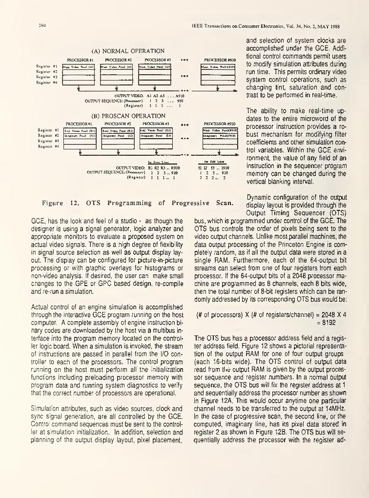
294 IEEE Transactions on Consumer Electronics, Vol. 34, No. 2, MAY 1988
(A) NORMAL OPERATION
PROCESSOR #1 PROCESSOR #2 PROCESSOR #3 PROCESSOR #910
Regiilcr #1 ^ui VicUo Puei (AI
Regisier #2
Rrginer #3
Regiiter «4
Mss V«)0o Pisel (A2 Video Pus) (A3 Mud Vid«o Pul(A910)
OlTTPirr VIDEa A1 A2 A3 .
.
OUTPUT SEQUENCE: (ProoMor) 12 3..(Regifler) 111..
(B) PROSCAN OPERATIONPROCESSOR #1 PROCESSOR #2 PROCESSOR #3
A9I0
910
1
PROCESSOR #910
Regiiier #1
#2
#3
#4
RcJ V«l«, Pi«£l (Rl)
Regiller IcQagsiary Pixel (11)
Regiiler
Regisier
Rckl Video Puid fR2)
lma«uiny Pixal (\2)
Ral Video Puxl (R3)
ltni£U)DT Pixel (13)
VluQ Video Pijtel(1l910
m^inuy Puiel(1910)
* ^
fcr Odd Lna
OUTPUT VIDEa Rl R2 R3 ... R910OUTPUTSEQUENCE:(ProcesiDr) i 2 3 ... 910
(Register) 1 1 1 ... 1
II 12 13 ..
1 2 3 ...
2 2 2 ...
1910
910
2
and selection of system clocks are
accomplished under the GCE. Addi-
tional control commands permit users
to modify simulation attributes during
run time. This permits ordinary video
system control operations, such as
changing tint, saturation and con-
trast to be performed in real-time.
The ability to make real-time up-
dates to the entire microword of the
processor instruction provides a ro-
bust mechanism for modifying filter
coefficients and other simulation con-
trol variables. Within the GCE envi-
ronment, the value of any field of an
instruction in the sequencer program
memory can be changed during the
vertical blanking interval.
Figure 12. OTS Programming of Progressive Scan.
GCE, has the look and feel of a studio - as though the
designer is using a signal generator, logic analyzer and
appropriate monitors to evaluate a proposed system on
actual video signals. There is a high degree of flexibility
in signal source selection as well as output display lay-
out. The display can be configured for picture-in-picture
processing or with graphic overlays for histograms or
non-video analysis. If desired, the user can make small
changes to the GPE or GPC based design, re-compile
and re-run a simulation.
Actual control of an engine simulation is accomplished
through the interactive GCE program running on the host
computer. A complete assembly of engine instruction bi-
nary codes are downloaded by the host via a multibus in-
terface into the program memory located on the control-
ler logic board. When a simulation is invoked, the stream
of instructions are passed in parallel from the I/O con-
troller to each of the processors. The control program
running on the host must perform all the initialization
functions including preloading processor memory with
program data and running system diagnostics to verify
that the correct number of processors are operational.
Simulation attributes, such as video sources, clock and
sync signal generation, are all controlled by the GCE.Control command sequences must be sent to the control-
ler at simulation initialization. In addition, selection and
planning of the output display layout, pixel placement,
Dynamic configuration of the output
display layout is provided through the
Output Timing Sequencer (OTS)
bus, which Is programmed under control of the GCE. The
OTS bus controls the order of pixels being sent to the
video output channels. Unlike most parallel machines, the
data output processing of the Princeton Engine is com-
pletely random, as if all the output data were stored in a
single RAM. Furthermore, each of the 64-output bit
streams can select from one of four registers from each
processor. If the 64-output bits of a 2048 processor ma-
chine are programmed as 8 channels, each 8 bits wide,
then the total number of 8-bit registers which can be ran-
domly addressed by its corresponding OTS bus would be:
(# of processors) X (# of registers/channel) = 2048 X 4
= 8192
The OTS bus has a processor address field and a regis-
ter address field. Figure 12 shows a pictorial representa-
tion of the output RAM for one of four output groups
(each 16-bits wide). The OTS control of output data
read from tlie output RAM is given by the output proces-
sor sequence and register numbers. In a normal output
sequence, the OTS bus will fix the register address at 1
and sequentially address the processor number as shown
in Figure 12A. This would occur anytime one particular
channel needs to be transferred to the output at 14MHz.
In the case of progressive scan, the second line, or the
computed, imaginary line, has its pixel data stored in
register 2 as shown in Figure 12B. The OTS bus will se-
quentially address the processor with the register ad-
Chin, et al.: The Princeton Engine: A Real-Time Video System Simulator 295
dress fixed at 1 and then change the register address to
2 at the end of the first line. The output sequence rate is
28f\/1Hz for progressive scan operation.
There are some cases in which it would be necessary to
use all four registers to generate the complete display. In
the case of a multiple Picture-in-a-Picture (PIP) simula-
tion, register 1 will store the main picture data and regis-
ters 2 through 4 will be used to store additional picture
inserts.
Running a simulation on the Princeton Engine requires as-
sembling three major GCE program segments. The first
segment is the SIMD program code, a run-time sequence
of instructions for the processing elements implementing
all the algorithms in the target system. This sequence of
instructions is the result of the design expansion of a
GPC-based description of the system. The second seg-
ment is the overall control program which must preload
any tables in processor memory, switch the appropriate
video sources and select the Output Timing Sequencer
registers. Wrapped around these two segments of the
GCE is a third segment which is an interactive program
running on the host computer. The engineer interacts
with this segment to organize the output, to change run-
time parameters and to start the simulation. This inter-
active segment must load the program and control seg-
ments into the controller and perform any of the multibus
operations necessary to transfer data and program, as
well as begin program execution.
Impiementation
Initial Princeton Engine systems will be comprised of a
sufficient number of processors to implement ACTV and
HDTV systems (1216 and 1536 processing elements, re-
spectively). A system is implemented in processor
boards each with 32 PROC IC's and 16 I/O IC's. The
processor boards are 22"x17", contain 12,000 holes and
have been implemented using high density discrete wire
technology. Each PROC IC contains two processing ele-
ments. The PROC and I/O IC's have been implemented
in two 75,000 gate, 1.5 micron, CMOS gate arrays.
Each IC is packaged in a 223 pin grid array. Local memo-ry consists of four 16Kx4 static RAMS per processor
which are contained on a daughter board assembly
mounted adjacent to each double processor IC.
The speed of the PROC IC is currently limited by the
gate-array designed multiplier. We believe that a custom
design of the PROC chip would realize instruction rates
around 30MHz.
An Engine cabinet contains eight processor boards for a
total of 512 processors. All controller and analog to digi-
tal interfaces are contained in a separate cabinet. A
1536 processor Princeton Engine consists of four small
cabinets and consumes two kilowatts of power.
Summary
This paper described a powerful parallel computer archi-
tecture which has been organized specifically for video
and image processing. This architecture combines a high
speed dual processor IC with an I/O IC specifically de-
signed to perform very high speed video simulation com-
putational tasks. The approach makes possible for the
first time, true, real-time simulations of very large video
systems and permits an entirely new design methodology
to be realized in which engineers can explore their design
ideas interactively. In addition, the system can be ex-
panded from a single 64-processor board up to a system
totaling 2048 processors, with full upward compatibility
of GPE/GPC based libraries and making the startup
cost low. The Princeton Engine system will be used in the
development of signal processing functions and features
for existing TV standards (NTSC, PAL,...), as well as
to define signal formats for ACTV and HDTV.
While the emphasis of this paper has been on an applica-
tion specific parallel computer, the SIMD architecture
used here is also applicable to the solution of a broad
range of problems. SIMD machines have been used to
solve a variety of problems including FFT's, terrain map-
ping, fluid dynamics [13], circuit simulation[14] and logic
simulation[15]. They have also been proposed for a va-
riety of other computational problems including IC pro-
cess and device simulation and animation.
Acknowtedaement
We would like to acknowledge the contributions to this
project of Robert Mature, Anthony Guyer, John Lee and
Smith Freeman. Bob and Tony were instrumental in see-
ing the system hardware of the Princeton Engine become
a reality. John kept all our computers working and Smith
helped produce test vectors for the PROC and I/O IC's.
We also wish to thank the Thomson/GE/RCA Consu-
mer Electronics Division for support of this work.

296 IEEE Transactions on Consumer Electronics, Vol. 34, No. 2, MAY 1988
References
1. Strolle.C.H., Smith.T.R., Reitmeier, G.A., and Bor-
chardt, R.P., "Digital Video Processing Facility with Mo-
tion Sequence Capability", International Conference on
Consumer Electronics Digest of Technical Papers, p.178,
June 1985.
2. Bernard, F. S., Law, K. A., "An Engineering Worksta-
tion and Video Frame-Store Peripheral for Simulating
Digital TV Signal Processing", RCA Review, Vol. 47,
March 1986, pp. 32-66.
3. Isnardi, M.A., Fuhrer, J.S., Smith, T.R., Koslov, J.L.,
Roeder, B.J., Wedam,W.F., "A Single Channel, NTSCCompatible Widescreen EDTV System", presented at
the HDTV Colloquium, Ottawa, Canada, Oct 4-8, 1987.
4. Hwang, K., "Advanced Parallel Processing with Su-
percomputer Architectures", Proceedings of the IEEE,
Vol. 75, No. 10, October 1987, pp. 1348-1379.
5. Hillis,W. D., "The Connection Machine", MIT Press,
Cambridge, Mass, 1985.
6. McMahon, E.P., "Applications of Fine Grain Parallel
Processing", Signal, April 1987, pp 69-74.
7. Enami, K., Yagi, N., and Murakami, K., "Real-Time
Video Signal Processor", SMPTE Journal, December
1987, pp. 1158-1165.
8. Fisher, A. L., "Scan Line Array Processors for Image
Computation", Computer Architecture News, Vol. 14,
No. 2, p. 338, June 1986.
9. Fisher, A. I., Highman, P.T., Rockoff, T.E.,
"Architecture of a VLSI SIMD Processing Element.",
ICCD, 1987.
10. Kung, H. T., Webb, Jon A., etal, "Warp Architecture
and Implementation", Conference Proceedings on the
13th Annual International Symposium on Computer Ar-
chitecture", 1986, pp. 346-356.
11. Kumar, V.K.P., Tsai,Y.C., "On Mapping Algorithms
to Linear and Fault Tolerant Systolic Arrays.", to ap-
pear in IEEE Transactions on Computers.
12. Rosenberg, A. "The Diogenes Approach to Testable
Fault-Tolerant Networks of Procesors.", IEEE Transac-
tions on Computers, CO-32, No.10, 1983, pp. 902-910.
13. Waltz, D.L., "Applications of the Connection Ma-
chine.", Computer, January 1987, pp 85-96.
14. Webber, D.M. and Sangiovanni-Vincentelli, A. "Circuit
Simulation on the Connection Machine." 24th ACM/IEEE
Design Automation Conference, 1987, pp 104-1 13.
15. Agrawal, P., Dally, W.J., Ezzat, A.K., Fischer, W.C,Jagadish, H.V., Krishnakumar, A.S., "Architecture and
Design of the MARS Hardware Accelerator", 24th
ACM/IEEE Design Automation Conference. 1987, pp.1 01-
107.

Chin, et al.: The Princeton Engine: A Real-Time Video System Simulator 297
Biographies :
Danny Chin (MTS) received a BSEE degree in 1979 and an MSEE degree in
1981, both from Columbia University. He joined the David Sarnoff Research
Center in 1979 where his work has covered digital TV tuning systems,VLSI de-
signs, automatic manufacturing methods, digital TV circuit designs including de-
lay line convergence, progressive scan and all aspects of chroma processing,
parallel computing architectures and real-time simulation. He has received
nine U.S. patents and one RCA Laboratories Outstanding Achievement award.
Stanley P. Knight (GH) received the BSEE degree from the University of
Kentucky in 1961 and the MSEE degree from Newark College of Engineering in
1969. In 1961, Mr. Knight joined RCA Astro-Electronics where he worked until
1970 on RF system and circuit design and the development of thin and thick film
technologies for microwave circuits. He worked at Zenith Radio from 1970 to
1973 on advanced TV tuner designs. He joined the David Sarnoff Research Center
in 1973 and became Group Head in 1977. He and his groups have been involved in
all aspects of TV receiver design. Since 1982 his group has concentrated on digital
signal processing functions and features for future digital TV's. He holds four USpatents and has received an IR100 Award for work on MIC's plus three RCA La-
boratories Outstanding Achievement awards.
Herb Taylor (MTS) received a B.A. in Physics in 1976 from Franklin and
Marshall College. He worked at Tl from 1977 to 1981 on various VLSI designs
relating to graphics and computers. He joined the David Sarnoff Research Center
in 1981 where he contributed to the development of a design methodology of VLSI
for digital television, to architectures for parallel computing and to a graphics
chip design for the RCA-GE DVI system. From 1985 until 1987, Mr. Taylor
represented RCA as a Member of the Technical Staff of the Microelectronics and
Computer Technology Corporation (MCC) in Austin, TX.
Joseph Passe (MTS) received a BSEE degree in 1967 and an MSEE degree in
1968, both from Rutgers University. He served as an officer in the United States
Marine Corps from 1969 to 1972. He held positions of Senior Engineer through
Staff Engineer from 1972 to 1985, working at TAL-STAR Computer Systems,
Autodynamics Inc., and Lockheed Electronics Co., Inc. where his work included all
phases of digital logic design for micro- and mini- computer based systems.
Since joining the David Sarnoff Research Center in 1985, he has been involved
in the design of digital TV signal processing circuits and parallel computing
architectures.
Francis S. Bernard (MTS) earned a BS degree in Electrical Engineering from
Rutgers University in 1982 and a MS degree in Electrical Engineering from
Georgia Institute of Technology in 1984. He joined the David Sarnoff Research
Center in 1984. His work has concentrated on digital signal processing and
features for digital TV including picture-in-a-picture, delay-line convergence,
field progressive scan systems and graphical programming techniques for parallel
computing architectures. He holds one US patent.

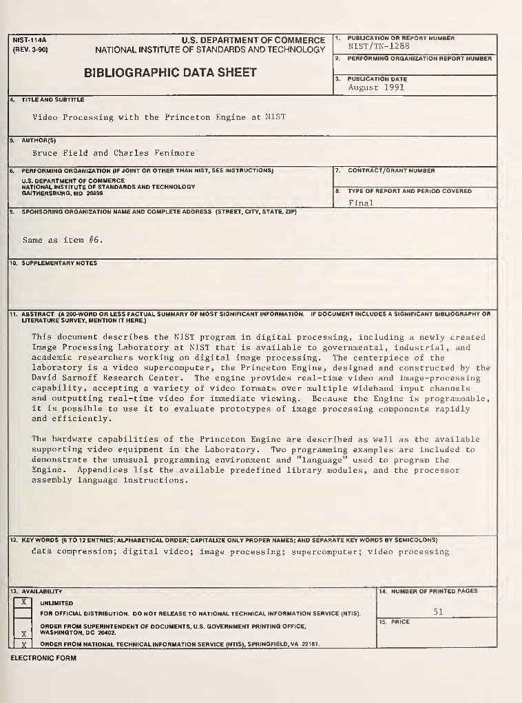
NIST-114A U.S. DEPARTMENT OF COMMERCE(REV. 3-90) NATIONAL INSTITUTE OF STANDARDS AND TECHNOLOGY
BIBLIOGRAPHIC DATA SHEET
1. PUBUCATION OR REPORT NUMBERNIST/TN-1288
PERFORMING ORQANIZATION REPORT NUMBER
3. PUBUCATION DATEAugust 1991
4. TITLE AND SUBTITLE
Video Processing with the Princeton Engine at NIST
5. AUTHOR(S)
Bruce Field and Charles Fenimore
6. PERFORMINO ORQANIZATION (IF JOINT OR OTHER THAN NIST, SEE INSTRUCTIONS)
U.S. DEPARTMENT OF COMMERCENATIONAL INSTITUTE OF STANDARDS AND TECHNOLOGYGAITHERSBURG, MD 20899
7. CONTRACT/GRANT NUMBER
8. TYPE OF REPORT AND PERIOD COVERED
Final9. SPONSORING ORGANIZATION NAME AND COMPLETE ADDRESS (STREET, CITY, STATE, ZIP)
Same as item #6.
10. SUPPLEMENTARY NOTES
11. ABSTRACT (A 200-WORD OR LESS FACTUAL SUMMARY OF MOST SIGNIFICANT INFORMATION. IF DOCUMENT INCLUDES A SIGNIFICANT BIBUOQRAPHY ORUTERATURE SURVEY, MENTION IT HERE.)
This document describes the NIST program in digital processing, including a newly createdImage Processing Laboratory at NIST that is available to governmental, industrial, andacademic researchers working on digital image processing. The centerpiece of thelaboratory is a video supercomputer, the Princeton Engine, designed and constructed by theDavid Sarnoff Research Center. The engine provides real-time video and image-processingcapability, accepting a variety of video formats over multiple wideband input channelsand outputting real-time video for immediate viewing. Because the Engine is programmable,it is possible to use it to evaluate prototypes of image processing components rapidlyand efficiently.
The hardware capabilities of the Princeton Engine are described as well as the availablesupporting video equipment in the Laboratory. Two programming examples are included to
demonstrate the unusual programming environment and "language" used to program theEngine. Appendices list the available predefined library modules, and the processorassembly language instructions.
12. KEY WORDS (6 TO 12 ENTRIES; ALPHABETICAL ORDER; CAPITAUZE ONLY PROPER NAMES; AND SEPARATE KEY WORDS BY SEMICOLONS)
data compression; digital video; image processing; supercomputer; video processing
13. AVAILABIUTY
UNUMITED
FOR OFFICIAL DISTRIBUTION. DO NOT RELEASE TO NATIONAL TECHNICAL INFORMATION SERVICE (NTIS).
X
JL
ORDER FROM SUPERINTENDENT OF DOCUMENTS, U.S. GOVERNMENT PRINTING OFFICE,WASHINGTON, DC 20402.
ORDER FROM NATIONAL TECHNICAL INFORMATION SERVICE (NTIS), SPRINGFIELD, VA 22161.
14. NUMBER OF PRINTED PAGES
5115. PRICE
ELECTRONIC FORM


U.S. Department of CommerceNational Institute of Standards and Technology
Gaithersburg, MD 20899
Official Business
Penalty for Private Use $300