zxld1321 boost mode dc-dc converter for led driving with · pdf fileboost mode dc-dc converter...
TRANSCRIPT

Issue 1 - January 2008 1 www.zetex.com© Zetex Semiconductors plc 2008
ZXLD1321
Boost mode DC-DC converter for LED driving with 1A
output and current control
Description
Note# : Using standard external components as specified under electrical characteristics. Efficiency is dependent uponexternal component types and values. Higher efficiency is possible with alternative coils.
The ZXLD1321 is an inductive DC-DCconverter, with an internal switch, designedfor driving single or multiple LEDs in series upto a total of 1A output current.
Applications cover commercial environmentswith input voltages ranging from 1.2V to 12V.
The device employs a variable 'on' and 'off'time control scheme with adjustable peakswitch current limiting and supports step-up(Boost) mode and self-powering Bootstrapoperating modes, offering higher powerefficiency and lower system cost thanconventional PFM circuitry.
The device includes the DC-DC converter, ahigh-side current monitor and an NPNswitching transistor to provide an integratedsolution offering small PCB size, competitivecost/performance, high power efficiency ofDC-DC conversion and maximum LEDbrightness/reliability. More importantly, itretains design flexibility to add customerspecific features.
The feedback control circuitry inside theZXLD1321 provides excellent load and currentregulation, resulting in very stable LED currentover the useful life of the battery and over thefull operating temperature range.
The LED current can be adjusted from 100%down to 10% of the set value by applying a dcvoltage to the ADJ pin and down to 1% byapplying a PWM signal to the ADJ pin. An on-chip LED protection circuit also allows outputcurrent to be reduced linearly above apredetermined threshold temperature using anexternal thermistor at the TADJ pin.
External resistors set nominal average LEDcurrent and coil peak current independently.
The device can be shut down by applying acontinuous low level dc voltage to the ADJ pin.
Features
• 1.2V to 12V Input voltage range
• Up to 1A output current
• Typical efficiency# >85%
• Bootstrap operation enables input voltagedown to 1V
• User-defined thermal control of LEDoutput current using external thermistor
• High output current stability over inputvoltage and temperature
• 12µA typical standby current
• LED current adjustable from 100% down to 2%
• Adjustable soft-start
• Drives up to 5 white LEDs in series
Applications
• High power LED flashlights
• LED back-up lighting
• General LED lighting
• Emergency lighting

ZXLD1321
Issue 1 - January 2008 2 www.zetex.com© Zetex Semiconductors plc 2008
Pin connections (top-view) Package view
Block diagram
Package
14-Pin DFN with exposed pad
4mm x 3mm
0.50mm pitch
1.5W @TA=70°C
DFN14 package (bottom view).
45° chamfer denotes Pin 1

ZXLD1321
Issue 1 - January 2008 3 www.zetex.com© Zetex Semiconductors plc 2008
Absolute maximum ratings
(Voltages relative to GND unless otherwise stated)
DC-DC converter
High-side current monitor
Switching NPN transistor
These are stress ratings only. Operation outside the absolute maximum ratings may cause device failure. Operation at the
absolute maximum ratings for extended periods may reduce device reliability.
Thermal resistance
Operating temperature (top) -40 to 125°C
Storage temperature (Tst) -55 to 150°C
Junction temperature (Tj) -40 to 150°C
Package power dissipation (Ptot)
DFN-14 with exposed pad: 4mmx3mm, 0.5mm Pitch 1.5W at Tamb = 70°C
Supply voltage (VIN) -0.3V to +12V
ADJ -0.3V to The lower of (+5.0V) or (VIN + 0.3V)
CFB -0.3V to The lower of (+5.0V) or (VIN + 0.3V)
ISENSE -0.3V to The lower of (+5.0V) or (VIN + 0.3V)
TADJ -0.3V to The lower of (+5.0V) or (VIN + 0.3V)
BIAS -0.3V to The lower of (+5.0V) or (VIN + 0.3V)
Monitor supply voltage (M_VIN) -0.3V to +18V
Continuous sense voltage
(M_VIN – M_LOAD)
-0.3V to +5V
Collector-Base voltage (VCBO) 18V
Collector-Emitter voltage (VCEO) 18V
Peak pulse current (ICM) 3A (Pulse width = 300µs. Duty cycle<=2%)
Continuous Collector current (IC) 2A
Junction to case (RUJC) Nominal value
DFN-14 26.3°C/W

ZXLD1321
Issue 1 - January 2008 4 www.zetex.com© Zetex Semiconductors plc 2008
Pin description
Name Pin # Description
ADJ 1 Adjust input
• Leave floating, or connect to VREF to set 100% output current.
• Drive with dc voltage. (50mV<VADJ< VREF) to adjust output
current from 10% to 100% of set value. (DC brightness control
mode)
• Drive with low frequency (200Hz) PWM control signal to gate
output ‘on’ and ‘off’ at the PWM frequency. (PWM brightness
control mode)
• Drive with low level dc voltage (VADJ<28mV) to turn off device
(Standby mode)
BIAS 2 Bias pin for setting base current of internal switch transistor
• Short pin to ground to define maximum base drive current for
output switch (Maximum output current condition)
• Connect resistor (RBIAS) from this pin to ground to reduce base
drive current (Reduced output current condition)
CFB 3 Compensation point
• Connect 10nF capacitor from this pin to ground to provide loop
compensation
N/C 4 No connection to this pin (open circuit)
ISENSE 5 Switch peak current sense pin
• Connect resistor (RSENSE) from this pin to ground to define peak
switch current (ISWPEAK)=VSENSE/RSENSE
EMITTER 6, 7 Switch emitters (connect both pins to top of RSENSE to sense emitter current)
COLLECTOR 8, 9 Switch collectors (connect both pins to lower side of coil)
M_LOAD 10 Load side input of high side current monitor
M_VIN 11 Input supply to high side current monitor
• Connect to output voltage (cathode of Schottky)
• Connect resistor (RM) between M_LOAD and M_VIN to define
nominal average output (LED) current of 0.1/RM
VIN 12 Positive supply to device (1.2-12V)
• Decouple to ground with capacitor close to device
TADJ 13 Temperature adjust input for LED thermal compensation
• Connect thermistor/resistor network to this pin to reduce output
current above a preset temperature threshold.
• Connect to VREF to disable thermal compensation function
(see section on temperature control for details)
VREF 14 Internal 0.5V reference voltage output
Exposed pad 15 Connect to ground (0V)

ZXLD1321
Issue 1 - January 2008 5 www.zetex.com© Zetex Semiconductors plc 2008
Electrical characteristics (Test conditions: VIN = 3V, TAMB= 25°C unless otherwise stated(a))
DC-DC converter supply parameters
NOTES:
(a) Production testing of the device is performed at 25°C. Functional operation of the device and parameters specified from -40°C to
+125°C are guaranteed by design, characterisation and process control.
(b) Between 1.2V and 2.2V the device will run in the Low Voltage Startup Mode (for details refer to section "Low Voltage Operation")
DC-DC converter input parameters
Symbol Parameter Conditions Min Typ Max Units
VIN Supply voltage Normal operation 2.0 12 V
VIN(Start) Supply voltage for start-up(b) Start-up mode 1.2 2.4 V
VUV- Under-voltage detection thresholdNormal operation to start-up mode
VIN falling 1.8 V
VUV+ Under-voltage detection thresholdStart-up mode to normal operation
VIN rising 2.2 V
Iq Quiescent current Measured into VINADJ pin floating.(Excluding switch base current).
1.5 mA
ISTBY Standby current Measured into VIN.ADJ pin grounded
12 20 µA
VREF Internal reference voltage ADJ pin floating2.0V<VIN<18V
480 500 520 mV
TCO(REF) Internal reference temperature coefficient.
50 ppm/K
Symbol Parameter Conditions Min Typ Max Units
VSENSE Peak switch current sense voltage
Measured on ISENSE pin CFB pin at 0V
45 55 65 mV
VSENSE
(SU)
Peak switch current sense voltage in start-up mode
Measured on ISENSE pin.Start-up modeVIN=1.2V
10.5 mV
ISENSE Sense input current Measured into ISENSE with pin at 0V. CFB pin at 0V
-15 -7 -1 µA
CFB Control loop compensation capacitor
10 nF
VADJ External dc control voltage applied to ADJ pin to adjust output current
DC brightness control mode
50 500 mV
VADJ(th) Switching threshold of ADJ pin
Standby state to normal operation
26 28 30 mV
TCO(VADJ) Temperature coefficient of VADJ(th)
+0.3 %/K
RADJ Internal resistor between VREF and ADJ
VADJ<500mV 100 kΩ
VADJ(clmp) Clamp voltage on ADJ pin 100µA injected into ADJ pin
575 mV

ZXLD1321
Issue 1 - January 2008 6 www.zetex.com© Zetex Semiconductors plc 2008
DC-DC converter output parameters
Switching NPN transistor
NOTES:
(c) Measured under pulse conditions.
(d) This current is measured via the collectors and emitters of the switch with these connected to ground (0V)
(e) Measured under pulse conditions. Peak Current = Ic
Symbol Parameter Conditions Min Typ Max Units
Toff(100) Discharge pulse width 100% output current 0.7 1.2 1.7 µs
Toff(10) Discharge pulse width 10% output current 4 8 12 µs
fLXmax Maximum operating
frequency
600 KHz
fSU Switching frequency in start-
up mode
VIN=1.2V 50 KHz
Symbol Parameter Conditions Min Typ Max Units
ISW Average continuous switch
current(c)
2 A
IBON(max) Maximum base current into
switch transistor from internal
drive circuit(d)
2V<VIN<18V
BIAS pin at 0V
30 50 70 mA
IBON Base current into switch
transistor using external
resistor (RBASE) from BIAS pin
to ground
RBIAS = 1680Ω 10 mA
V(BR)CEO Collector-Emitter breakdown
voltage
IC=10µA 20 V
VCE(sat) Collector-Emitter saturation
voltage
IC=0.1A, IB=10mA
IC=2A, IB=50mA(e)
50
120
mV
mV
hFE Static forward current transfer
ratio
IC=200mA, VCE=2V
IC=2A, VCE=2V
209
116
COBO Output capacitance VCB=10V,f=1MHz 64 pF
t(on) Turn-on time Ic=0 to IC=2A
VIN=10V
30 ns
t(off) Turn-off time IC=2A to Ic<100µA 28 ns

ZXLD1321
Issue 1 - January 2008 7 www.zetex.com© Zetex Semiconductors plc 2008
High-side current monitor
Reference current monitor
LED thermal control circuit (TADJ) parameters
Symbol Parameter Conditions Min Typ Max Units
VM_VIN Supply voltage 3 18 V
VMON Sense voltage =V(M_VIN) – V(M_LOAD) 0 100 200 mV
IM_LOAD Input current Measured into M_LOAD pin 0.08 1 µA
TCO(MON)
Temperature coefficient VMON=10mV
VMON=100mV
370
150
ppm/
K
BW Bandwidth VMON=10mV
VMON=100mV
350
2.5
KHz
MHz
Gm Transconductance
DIout/DVMON
1 mA/V
Acc Accuracy RM = 0.1ΩVMON = 100mV
-3 3 %
Symbol Parameter Conditions Min Typ Max Units
VADJ Adjust Voltage 0 500 mV
TCO
(MON)
Temperature Coefficient VADJ=50mV
VADJ=500mV
160
200
ppm/
K
BW Bandwidth VADJ=50mV
VADJ=500mV
275
3
KHz
MHz
Gm Transconductance
DIout/DVADJ
200 µA/V
Acc Accuracy VADJ=500mV -3 3 %
Symbol Parameter Conditions Min Typ Max Units
VTADJH Upper threshold voltage Onset of output current
reduction (VTADJ falling)
75 mV
VTADJL Lower threshold voltage Output current reduced to
<10% of set value
(VTADJ falling)
50 mV
Gm(TADJ) Transconductance
DIout/DVTADJ
4 mA/V

ZXLD1321
Issue 1 - January 2008 8 www.zetex.com© Zetex Semiconductors plc 2008
Output current regulation parameters
NOTES:
(f) System parameter only. This value is dependent upon external components and circuit configuration.
(g) This refers to the accuracy of output current regulation under normal operation when the feedback loop incorporating
the current monitor is active. The tolerances of external components are not included in this figure.
Ordering information
Symbol Parameter Conditions Min Typ Max Units
IOUT Minimum output/
LED current(f)VIN>3V 2 A
DIOUT Output current accuracy(g) 3.0V<VIN<12V,
Iout=1A,
VADJ=100mV
-5 +5 %
TCO
I(OUT)
Output current
temperature drift
3.0V<VIN<12V,
Iout=1A,
VADJ=100mV
100 200 ppm/
K
DIOUT/
IOUT
Load current regulation 350mA<I(LED)<1A 2 %/A
DIOUT/
DVIN
Line voltage regulation of
output current
0.5 %/V
Eff Efficiency(f) 350mA<I(LED)<1A 85 %
Device Reel size
(mm)
Reel width
(mm)
Quantity
per reel
Device mark
ZXLD1321DCATC 33.02 12 3,000 1321

ZXLD1321
Issue 1 - January 2008 9 www.zetex.com© Zetex Semiconductors plc 2008
Device description
The ZXLD1321 is a inductive boost DC-DC converter, with an internal switch, designed for driving
single or multiple LEDs in series up to a total of 1A output current. Depending upon supply
voltage (VIN), LED forward voltage drop (VLED) and circuit configuration, this can provide up to
8W of output power.
Applications cover VIN ranging from 1.2V to 12V.
The device employs a modified Pulse Frequency Modulation (PFM) control scheme, with variable
"ON" and "OFF" time control and adjustable peak switch current limiting.
General device operation (refer to block diagram)
Normal operation
Control is achieved by sensing the LED current in a series resistor (RM), connected between the
two inputs of the LED Current Monitor. This generates a proportional current (IMON) that charges
the external integrator capacitor CFB. IMON is balanced against a reference discharge current (IADJ)
generated at the output of a second voltage to current converter driven from the demand voltage
(VADJ) on the ADJ pin. The difference between IMON and IADJ is integrated by CFB to produce an
error voltage. A comparator takes a summed version of the voltage at the ISENSE pin and a
fraction of this CFB voltage and resets the latch driving the switch when the sum is greater than
50mV. The switch transistor is turned on by the output of the SR latch, which remains set until the
emitter current in the switch transistor produces a voltage drop Vsense (=50mV nominal) in
external resistor Rsense, defining a preset maximum switch current of 50mV/Rsense. Operation
is such that a rising error voltage on CFB will effectively lower the voltage required on the ISENSE
pin and therefore reset the latch earlier in the switching cycle. This will reduce the 'ON' time of
the switch and reduce the peak current in the switch from its preset maximum value. Similarly, a
falling error voltage will reset the latch later and the peak switch current will be increased. The
control loop therefore reduces or increases the energy stored in the coil during each switching
cycle, as necessary, to force the LED current to the set value. This results in high accuracy, as no
error is needed in the LED current to drive the servo to the required region.
The time taken for the coil current to reach the peak value depends on several factors: the supply
voltage, the peak coil current required at that particular LED power and whether the system
operates in "continuous" or "discontinuous" mode. The time allowed for the coil current to
discharge into the LED is fixed by the 'Variable Off Delay' monostable, whose period is modified
by the power demand signal on the ADJ pin. This monostable determines the time for which the
latch remains reset (switch off) and provides a longer "OFF" period at lower power settings,
helping to keep the parameters within an acceptable range.
Note that the "ON" period and the "OFF" period are set by the supply voltage, LED power and
external components chosen. The frequency is therefore determined by these parameters and is
NOT fixed. In this modified PFM scheme, the external components can be chosen to keep the
frequency well above the audio range for all extremes of parameters, so no audible whistling
should ever occur.
The 500mV reference voltage defines the nominal VADJ voltage and this defines the 100% output
current. For lower LED currents, the ADJ pin can be-driven from an external dc voltage
(50mV<VADJ<500mV) or a low frequency Pulse Width Modulated (PWM) waveform.

ZXLD1321
Issue 1 - January 2008 10 www.zetex.com© Zetex Semiconductors plc 2008
Low voltage operation (start-up mode)
For supply voltages below 2V, the normal control loop will have insufficient headroom to operate
reliably. This condition is detected by the 'under-voltage comparator', which compares a fraction
of the internal supply voltage (Vcc) against VREF. When the comparator output is active
(Vcc<1.8V), the output of the normal switch drive circuit is disabled and an alternative 'Start-up
oscillator and driver' enabled. The start-up oscillator provides a nominal 50kHz fixed frequency
drive signal to the base of the switch transistor, which is independent of VADJ and the voltage on
CFB. Under low voltage conditions, the peak current in the coil ramps to approximately 25% of
the normal value and the "OFF" time is fixed.
The low voltage start-up mode allows the device to operate down to 1.2V nominal. This allows
the chip to work from a single cell in boost mode and by configuring the device in Bootstrap
mode, normal operation of the control loop will occur once the output has risen above 2.2V.
Details of Bootstrap-Boost mode are given in the application notes.
ADJ pin
The ADJ pin is connected to the internal 500mV reference (VREF) via a 100k resistor. This biases
the ADJ pin to the reference voltage and defines nominal 100% LED current.
The ADJ pin can be overdriven with an external dc voltage between 50mV and 500mV to reduce
the LED current proportionally between 10% and 100% of the nominal value.
LED current can also be adjusted by applying a low frequency PWM signal to the ADJ pin to turn
the device On and Off. This will produce an average output current proportional to the duty cycle
of the control signal.
The device can be shut down by shorting the ADJ pin to ground, or pulling it to a voltage below
28mV with a suitable open collector NPN or open drain NMOS transistor. In the shutdown state,
most of the circuitry inside the device is switched off and residual quiescent current will be
typically 12µA.
Thermal control of LED current
The 'Thermal compensation current' circuit produces a sourcing current (Itc) which is zero for
voltages above 75mV on TADJ and increases to 100µA when TADJ falls to 50mV. This current is
summed into the control node and subtracted from the demand current, causing LED current to
reduce from 100% down to zero over this input range. The potential divider, consisting of a fixed
resistor Rt and an NTC Thermistor Rth between VREF and ground, defines the voltage on TADJ
and sets the threshold temperature. Further details are given in the application notes.
The Thermal Control feature can be disabled by leaving the TADJ pin floating, or by connecting
it to VREF.
Over-temperature shutdown
The ZXLD1321 incorporates an over-temperature shutdown circuit to protect the device against
damage caused by excess die temperature, resulting from excessive power dissipation in the
switch. The output of the 'Over-temp Shutdown' circuit will go high when the die temperature
exceeds 150°C (nominal). This will turn off the drive to the switch during normal operation.
Operation will resume when the device has cooled to a safe level.

ZXLD1321
Issue 1 - January 2008 11 www.zetex.com© Zetex Semiconductors plc 2008
Application notes
Setting peak coil current
The peak current in the coil is set by the resistor (RSENSE) between the switch emitter and ground
according to
The minimum peak current will depend on operating mode, coil inductance and supply voltage
range. The maximum peak current must not exceed the specified value for the switch. (See
Application circuits for details).
Setting LED current
The nominal average LED current is given by
Where RM is the external resistor connected between pins M_VIN and M_LOAD.
This current can be adjusted to a lower value by applying a dc control voltage or PWM control
signal to the ADJ pin.
DC control
The LED current can be adjusted over a 10% to 100% range by connecting a variable resistor RADJ
from the ADJ pin to ground to vary the dc voltage at the ADJ pin. RADJ forms the lower part of a
resistive divider and the internal 100kΩ resistor between the ADJ and VREF pins forms the upper
part. A value of 1MΩ for RADJ will therefore give a maximum current of 91% of ILED (nom) and
the device will be turned off when the voltage on the ADJ pin falls below 28mV, corresponding to
an RADJ value of approximately 5kΩ. If required, an end-stop resistor in series with RADJ can be
used to maintain the voltage on the ADJ pin above the turn-on threshold.
Using a logarithmic potentiometer for RADJ will give an approximately linear variation of output
current with shaft rotation. (Fig 1)
If required, the maximum output current can be restored to 100% by adjusting the value of the
LED current monitor resistor (RM). The tolerance of the internal 100k resistor and RADJ should be
taken into account when calculating output current.
The ADJ pin is clamped internally to a voltage of 575mV (nom), to limit maximum average output
current to approximately 115% of ILED(nom).
Rsense
mVI SWpeak
50=
MLED R
mVnomI
100)( =

ZXLD1321
Issue 1 - January 2008 12 www.zetex.com© Zetex Semiconductors plc 2008
Fig 1
PWM control
A wider dimming range can be achieved by applying a PWM control signal to the ADJ pin to turn
the device on and off, giving an average output current proportional to the duty cycle of the
control signal. The ADJ pin can be driven directly from the open drain NMOS output of a
microcontroller, or indirectly with a low saturation voltage NPN transistor such as the Zetex
ZXTN25015DFH. (Fig 2).
Fig 2
In the circuit of Fig 4, the average LED output current will be
Where duty cycle
A PWM frequency of 200Hz, or lower is recommended, to minimize errors due to the rise and fall
times of the converter output.
ZXLD1321ADJ
ZXTN25015DFH
DnomIavgI LEDLED *)()( =
)21(
2
TT
TD
+=
ZXLD1321
Issue 1 - January 2008 13 www.zetex.com© Zetex Semiconductors plc 2008
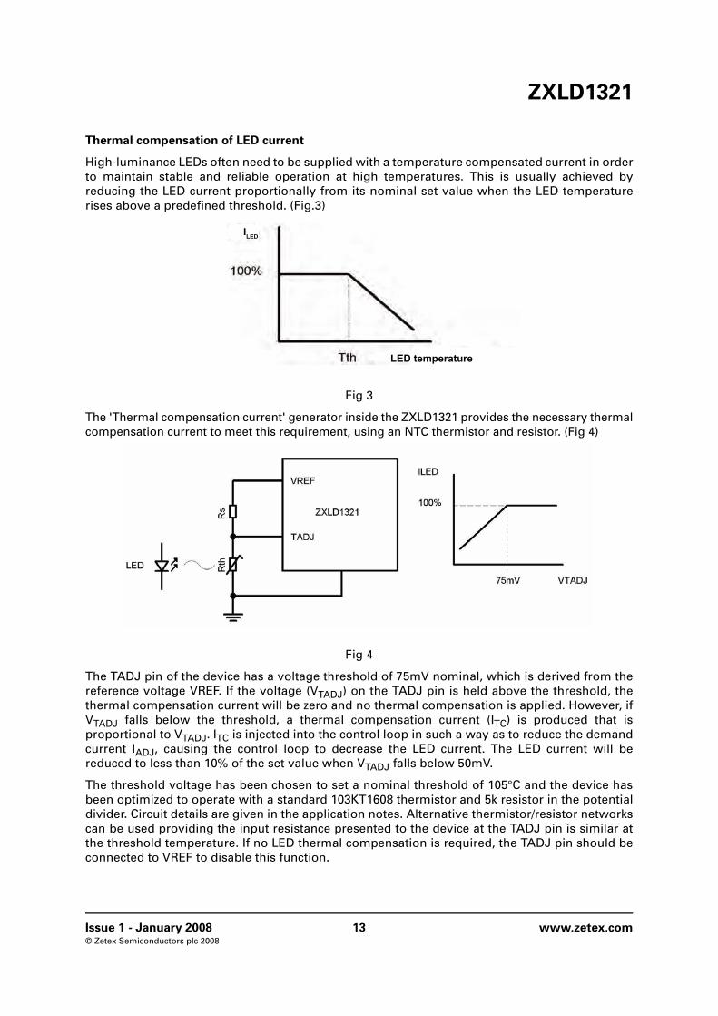
Thermal compensation of LED current
High-luminance LEDs often need to be supplied with a temperature compensated current in order
to maintain stable and reliable operation at high temperatures. This is usually achieved by
reducing the LED current proportionally from its nominal set value when the LED temperature
rises above a predefined threshold. (Fig.3)
Fig 3
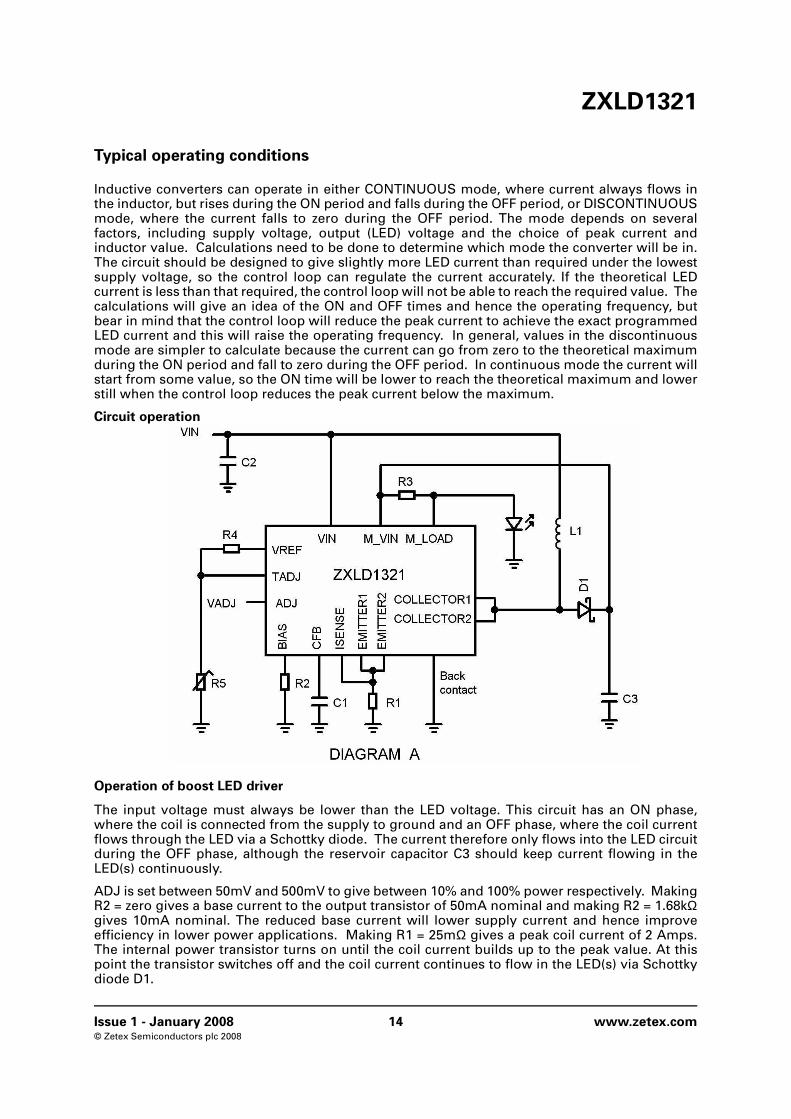
The 'Thermal compensation current' generator inside the ZXLD1321 provides the necessary thermal
compensation current to meet this requirement, using an NTC thermistor and resistor. (Fig 4)
Fig 4
The TADJ pin of the device has a voltage threshold of 75mV nominal, which is derived from the
reference voltage VREF. If the voltage (VTADJ) on the TADJ pin is held above the threshold, the
thermal compensation current will be zero and no thermal compensation is applied. However, if
VTADJ falls below the threshold, a thermal compensation current (ITC) is produced that is
proportional to VTADJ. ITC is injected into the control loop in such a way as to reduce the demand
current IADJ, causing the control loop to decrease the LED current. The LED current will be
reduced to less than 10% of the set value when VTADJ falls below 50mV.
The threshold voltage has been chosen to set a nominal threshold of 105°C and the device has
been optimized to operate with a standard 103KT1608 thermistor and 5k resistor in the potential
divider. Circuit details are given in the application notes. Alternative thermistor/resistor networks
can be used providing the input resistance presented to the device at the TADJ pin is similar at
the threshold temperature. If no LED thermal compensation is required, the TADJ pin should be
connected to VREF to disable this function.
ILED
LED temperature
ZXLD1321
Issue 1 - January 2008 14 www.zetex.com© Zetex Semiconductors plc 2008
Typical operating conditions
Inductive converters can operate in either CONTINUOUS mode, where current always flows inthe inductor, but rises during the ON period and falls during the OFF period, or DISCONTINUOUSmode, where the current falls to zero during the OFF period. The mode depends on severalfactors, including supply voltage, output (LED) voltage and the choice of peak current andinductor value. Calculations need to be done to determine which mode the converter will be in.The circuit should be designed to give slightly more LED current than required under the lowestsupply voltage, so the control loop can regulate the current accurately. If the theoretical LEDcurrent is less than that required, the control loop will not be able to reach the required value. Thecalculations will give an idea of the ON and OFF times and hence the operating frequency, butbear in mind that the control loop will reduce the peak current to achieve the exact programmedLED current and this will raise the operating frequency. In general, values in the discontinuousmode are simpler to calculate because the current can go from zero to the theoretical maximumduring the ON period and fall to zero during the OFF period. In continuous mode the current willstart from some value, so the ON time will be lower to reach the theoretical maximum and lowerstill when the control loop reduces the peak current below the maximum.
Circuit operation
Operation of boost LED driver
The input voltage must always be lower than the LED voltage. This circuit has an ON phase,where the coil is connected from the supply to ground and an OFF phase, where the coil currentflows through the LED via a Schottky diode. The current therefore only flows into the LED circuitduring the OFF phase, although the reservoir capacitor C3 should keep current flowing in theLED(s) continuously.
ADJ is set between 50mV and 500mV to give between 10% and 100% power respectively. MakingR2 = zero gives a base current to the output transistor of 50mA nominal and making R2 = 1.68kΩgives 10mA nominal. The reduced base current will lower supply current and hence improveefficiency in lower power applications. Making R1 = 25mΩ gives a peak coil current of 2 Amps.The internal power transistor turns on until the coil current builds up to the peak value. At thispoint the transistor switches off and the coil current continues to flow in the LED(s) via Schottkydiode D1.

ZXLD1321
Issue 1 - January 2008 15 www.zetex.com© Zetex Semiconductors plc 2008
The LED current is sensed by R3 and the controller varies this until the drop in R3 equals 20% of
VADJ. Hence making R3 = 100mΩ and VADJ = 500mV gives a LED current of 1 Amp because the
500mV VADJ results in 100mV across R3 which equals 1 Amp. Making VADJ = 10mV gives a LED
current of 100mA because the 50mV VADJ results in 10mV drop across R3 which equals 100mA.
The power is controlled by the chip backing off the peak coil current, so it is necessary to calculate
the coil inductance and current to guarantee slightly more than 100% LED power, so the circuit
can control it effectively. The internal control loop is compensated by C1, which is normally 10nF.
If the thermistor (R5) is used, the power will be backed off progressively as the TADJ pin goes low.
With the TADJ pin above 75mV, power is 100% and this is reduced to zero when the TADJ pin
reaches 50mV. Making R4 = 5kΩ and using a 103KT1608 thermistor, the thermistor will reach 869Ωat 105°C giving VTADJ = 74mV which will start to reduce the LED power above 105°C. By 125°C the
thermistor will reach 547Ω giving VTADJ = 50mV which gives zero power. This will protect the LED
from damage. These temperature values can be set by the customer by using a different
thermistor or a different value of R4. If protection is not required, leaving the TADJ pin open circuit
will make it float to a high voltage and always give 100% power.
Reference Part No Value Manufacturer Contact Details
U1 ZXLD1321 LED Driver Zetex www.zetex.com
D1 ZXCS2000 Schottky diode Zetex
L1 MSS7341-103ML 10µH 2A Coilcraft www.coilcraft.co
m
L1 NPIS64D100MTRF 10µH 2A NIC www.niccomp
L1 744 77810 10µH 2A Wurth www.wurth.co.uk
C1 Generic 10nF 10V Generic
C2 GRM31CR71H475K 4.7µF 50V Murata 1206 www.murata.com
C3 GRM31MR71E225K 2.2µF 25V Murata 1206 www.murata.com
R1 Generic 25mΩ Generic 0805
R2 Generic Generic 0603
R3 Generic 100mΩ Generic 0805
R4 Generic 5.1kΩ Generic 0603
R5 Thermistor NTC 10k 103kt1608
ZXLD1321
Issue 1 - January 2008 16 www.zetex.com© Zetex Semiconductors plc 2008
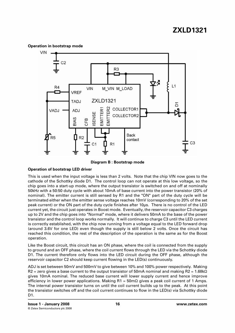
Operation in bootstrap mode
Diagram B : Bootstrap mode
Operation of bootstrap LED driver
This is used when the input voltage is less than 2 volts. Note that the chip VIN now goes to the
cathode of the Schottky diode D1. The control loop can not operate at this low voltage, so the
chip goes into a start-up mode, where the output transistor is switched on and off at nominally
50kHz with a 50:50 duty cycle with about 10mA of base current into the power transistor (20% of
nominal). The emitter current is still sensed by R1 and the "ON" part of the duty cycle will be
terminated either when the emitter sense voltage reaches 10mV (corresponding to 20% of the set
peak current) or the ON part of the duty cycle finishes after 10µs. There is no control of the LED
current yet, the circuit just operates in Boost mode. Eventually, the reservoir capacitor C3 charges
up to 2V and the chip goes into "Normal" mode, where it delivers 50mA to the base of the power
transistor and the control loop works normally. It will continue to charge C3 until the LED current
is correctly established, with the chip now running from a voltage equal to the LED forward drop
(around 3.6V for one LED) even though the supply is still below 2 volts. Once the circuit has
reached this condition, the rest of the description of the operation is the same as for the Boost
operation.
Like the Boost circuit, this circuit has an ON phase, where the coil is connected from the supply
to ground and an OFF phase, where the coil current flows through the LED via the Schottky diode
D1. The current therefore only flows into the LED circuit during the OFF phase, although the
reservoir capacitor C2 should keep current flowing in the LED(s) continuously.
ADJ is set between 50mV and 500mV to give between 10% and 100% power respectively. Making
R2 = zero gives a base current to the output transistor of 50mA nominal and making R2 = 1.68kΩgives 10mA nominal. The reduced base current will lower supply current and hence improve
efficiency in lower power applications. Making R1 = 50mΩ gives a peak coil current of 1 Amps.
The internal power transistor turns on until the coil current builds up to the peak. At this point
the transistor switches off and the coil current continues to flow in the LED(s) via Schottky diode
D1.

ZXLD1321
Issue 1 - January 2008 17 www.zetex.com© Zetex Semiconductors plc 2008
The LED current is sensed by R3 and the controller varies this until the drop in R3 equals 20% of
VADJ. Hence making R3 = 100mΩ and VADJ = 500mV gives a LED current of 1 Amp because the
500mV VADJ results in 100mV across R3 which equals 1 Amp. Making VADJ = 10mV gives a LED
current of 100mA because the 50mV VADJ results in 10mV drop across R3 which equals 100mA.
The power is controlled by the chip backing off the peak coil current, so it is necessary to calculate
the coil inductance and current to guarantee slightly more than 100% LED power, so the circuit
can control it effectively. The internal control loop is compensated by C1, which is normally 10nF.
Note that in Bootstrap mode, the input current will be 2 or 3 times larger than the LED current and
the duty cycle will be such that TON is larger than TOFF, due to the fact that the supply voltage
charging the coil is low. Because of this, large LED currents can not be programmed at very low
supply voltages, as the transistor current would need to exceed 2 Amps.
If the thermistor (R5) is used, the power will be backed off progressively as the TADJ pin goes low.
With the TADJ pin above 75mV, power is 100% and this is reduced to zero when the TADJ pin
reaches 50mV. Making R4 = 5kΩ and using a 103KT1608 thermistor, the thermistor will reach
869Ω at 105°C giving TADJ = 74mV which will start to reduce the LED power above 105°C. By
125°C the thermistor will reach 547Ω giving TADJ = 50mV which gives zero power. This will
protect the LED from damage. These temperature values can be set by the customer by using a
different thermistor or a different value of R4. If protection is not required, leaving the TADJ pin
open circuit will make it float to a high voltage and always give 100% power.
Reference Part No Value Manufacturer Contact Details
U1 ZXLD1321 LED Driver Zetex www.zetex.com
D1 ZXCS2000 Schottky diode Zetex
L1 MSS7341-103ML 10µH 2A Coilcraft www.coilcraft.co
m
L1 NPIS64D100MTRF 10µH 2A NIC www.niccomp
L1 744 777910 10µH 2A Wurth www.wurth.co.uk
C1 Generic 10nF 10V Generic
C2 GRM31CR71H475K 4.7µF 50V Murata 1206 www.murata.com
C3 GRM31MR71E225K 2.2µF 25V Murata 1206 www.murata.com
R1 Generic 25mΩ Generic 0805
R2 Generic Generic 0603
R3 Generic 100mΩ Generic 0805
R4 Generic 5.1kΩ Generic 0603
R5 Thermistor NTC 10k 103kt1608
ZXLD1321
Issue 1 - January 2008 18 www.zetex.com© Zetex Semiconductors plc 2008
Additional notes which apply to all operational modes
Note with all these circuits that the ON time is set by the time it takes the coil to reach the peak
current. This peak value is reduced by the control loop to give the desired LED power, so the ON
time can vary over a wide range. The minimum coil current can be zero (discontinuous operation)
or finite (continuous operation) depending on the supply voltage, LED current and the LED
voltage. The OFF time is set by an internal timer and is nominally 1.2µs at 100% LED power (VADJ
= 500mV), increasing to about 8µs at 10% LED power (VADJ = 50mV). The longer OFF time and
variable peak current enables the circuit to dim the LED whilst maintaining continuous switching,
rather than "skipping" or stalling and continuous running is better for reducing electrical noise
and also for eliminating audible noise from the coil core.
Layout considerations
As with all switching DC to DC converters, the currents can be large. Using small inductors with
a reasonably high supply voltage will cause currents to change quickly. High dI/dt can cause
inductively-coupled spikes into adjacent tracks. At the transition from of the ON phase to the OFF
phase and back, where the power transistor switches, the voltage at the collector rises and falls
quickly. High dV/dt can cause capacitively coupled spikes into adjacent tracks, especially if they
have a high impedance. For this reason, all tracks on the PCB should be thick, to minimise drops,
and short to keep all the components coupled tightly together.
A double-sided board should be used with a ground plane to screen the tracks and provide a good
ground return for the various functions and the rear exposed pad on the package should have an
appropriately-sized land with good ground connections, both to reduce electrical noise due to
ground drops and to improve thermal conductivity.
The input decoupling capacitor C1 should be very close to the chip pins and the LED sense
resistor R3 should have Kelvin tracks to M_VIN and M_LOAD to achieve LED current
measurement accuracy, as the PCB tracks will have comparable resistance to the 100mΩ resistor,
so taking sense tracks to the current monitor which are not connected close to the ends of R3 will
cause a measurement error.
The peak current sense resistor R1 should have short tracks to the ground at the bottom end and
Kelvin tracks to ISENSE at the top end. This resistor might need to be only 25mΩ and PCB track
resistance becomes comparable if the tracks are not very short. ISENSE is a high impedance
input, so a thin track from this pin directly to the top of RSENSE resistor R1 will still give an accurate
measurement.
The ADJ pin should have short tracks, as this is a fairly low-level signal controlling the power of
the system. As it needs to be less than 28mV for shutdown, a close ground connection is needed
for the pull-down device, as any ground drops could raise the potential. In particular, if a bipolar
transistor is used as a pull-down device, this will have an appreciable VSAT, which could perhaps
be half the shutdown potential.
The bottom of the thermistor must be coupled very closely to ground, as the TADJ pin varies the
LED current from 100% to 0% for a voltage change of only 25mV, so any noise on the bottom of
the thermistor will seriously affect the accuracy of the Thermal Protection circuit.

ZXLD1321
Issue 1 - January 2008 19 www.zetex.com© Zetex Semiconductors plc 2008
Package outline - DFN14 (4x3x0.75)
Note: Controlling dimensions are in millimeters. Approximate dimensions are provided in inches
DIM Inches Millimeters DIM Inches Millimeters
Min Max Min Max Min Max Min Max
A 0.0276 0.0315 0.70 0.80 D2 0.1240 0.1279 3.15 3.25
A1 0.00 0.002 0.00 0.05 e 0.0197 BSC 0.50 BSC
A3 0.008 REF. 0.203 REF. E 0.1161 0.1201 2.95 3.05
b 0.0079 0.0118 0.20 0.30 E2 0.0650 0.0689 1.65 1.75
D 0.1555 0.1594 3.95 4.05 L 0.0138 0.0177 0.35 0.45
E
D
A
A1
A3
D2
b
L
E2
60.3938
PIN 1 DOTBY MARKING
CHAMFER 0.300 X 45°
PIN #1 IDENTIFICATION

ZXLD1321
Issue 1 - January 2008 20 www.zetex.com© Zetex Semiconductors plc 2008
Zetex sales offices
Europe
Zetex GmbHKustermann-parkBalanstraße 59D-81541 MünchenGermanyTelefon: (49) 89 45 49 49 0Fax: (49) 89 45 49 49 [email protected]
Americas
Zetex Inc700 Veterans Memorial HighwayHauppauge, NY 11788USA
Telephone: (1) 631 360 2222Fax: (1) 631 360 [email protected]
Asia Pacific
Zetex (Asia Ltd)3701-04 Metroplaza Tower 1Hing Fong Road, Kwai FongHong Kong
Telephone: (852) 26100 611Fax: (852) 24250 [email protected]
Corporate Headquarters
Zetex Semiconductors plcZetex Technology Park, ChaddertonOldham, OL9 9LLUnited Kingdom
Telephone: (44) 161 622 4444Fax: (44) 161 622 [email protected]
© 2008 Published by Zetex Semiconductors plc
Definitions
Product change
Zetex Semiconductors reserves the right to alter, without notice, specifications, design, price or conditions of supply of any product or
service. Customers are solely responsible for obtaining the latest relevant information before placing orders.
Applications disclaimer
The circuits in this design/application note are offered as design ideas. It is the responsibility of the user to ensure that the circuit is fit for
the user’s application and meets with the user’s requirements. No representation or warranty is given and no liability whatsoever is
assumed by Zetex with respect to the accuracy or use of such information, or infringement of patents or other intellectual property rights
arising from such use or otherwise. Zetex does not assume any legal responsibility or will not be held legally liable (whether in contract,
tort (including negligence), breach of statutory duty, restriction or otherwise) for any damages, loss of profit, business, contract,
opportunity or consequential loss in the use of these circuit applications, under any circumstances.
Life support
Zetex products are specifically not authorized for use as critical components in life support devices or systems without the express written
approval of the Chief Executive Officer of Zetex Semiconductors plc. As used herein:
A. Life support devices or systems are devices or systems which:
1. are intended to implant into the body
or 2. support or sustain life and whose failure to perform when properly used in accordance with instructions for use provided in the
labelling can be reasonably expected to result in significant injury to the user.
B. A critical component is any component in a life support device or system whose failure to perform can be reasonably expected to
cause the failure of the life support device or to affect its safety or effectiveness.
Reproduction
The product specifications contained in this publication are issued to provide outline information only which (unless agreed by the
company in writing) may not be used, applied or reproduced for any purpose or form part of any order or contract or be regarded as a
representation relating to the products or services concerned.
Terms and Conditions
All products are sold subjects to Zetex’ terms and conditions of sale, and this disclaimer (save in the event of a conflict between the two
when the terms of the contract shall prevail) according to region, supplied at the time of order acknowledgement.
For the latest information on technology, delivery terms and conditions and prices, please contact your nearest Zetex sales office.
Quality of product
Zetex is an ISO 9001 and TS16949 certified semiconductor manufacturer.
To ensure quality of service and products we strongly advise the purchase of parts directly from Zetex Semiconductors or one of our
regionally authorized distributors. For a complete listing of authorized distributors please visit: www.zetex.com/salesnetwork
Zetex Semiconductors does not warrant or accept any liability whatsoever in respect of any parts purchased through unauthorized sales channels.
ESD (Electrostatic discharge)
Semiconductor devices are susceptible to damage by ESD. Suitable precautions should be taken when handling and transporting devices.
The possible damage to devices depends on the circumstances of the handling and transporting, and the nature of the device. The extent
of damage can vary from immediate functional or parametric malfunction to degradation of function or performance in use over time.
Devices suspected of being affected should be replaced.
Green compliance
Zetex Semiconductors is committed to environmental excellence in all aspects of its operations which includes meeting or exceeding
regulatory requirements with respect to the use of hazardous substances. Numerous successful programs have been implemented to
reduce the use of hazardous substances and/or emissions.
All Zetex components are compliant with the RoHS directive, and through this it is supporting its customers in their compliance with
WEEE and ELV directives.
Product status key:
“Preview” Future device intended for production at some point. Samples may be available
“Active” Product status recommended for new designs
“Last time buy (LTB)” Device will be discontinued and last time buy period and delivery is in effect
“Not recommended for new designs” Device is still in production to support existing designs and production
“Obsolete” Production has been discontinued
Datasheet status key:
“Draft version” This term denotes a very early datasheet version and contains highly provisional information, whichmay change in any manner without notice.
“Provisional version” This term denotes a pre-release datasheet. It provides a clear indication of anticipated performance.However, changes to the test conditions and specifications may occur, at any time and without notice.
“Issue” This term denotes an issued datasheet containing finalized specifications. However, changes tospecifications may occur, at any time and without notice.