x64-lvds user's manual - adstec · 2015-07-10 · x64-lvds user's manual x64-lvds...
TRANSCRIPT
DALSA Montreal • 7075 Place Robert-Joncas, Suite 142 • St-Laurent, Quebec, H4M 2Z2 • Canada http://www.imaging.com/
*OC-64LM-USER0*
X64-LVDS™
User's Manual
Part number OC-64LM-USER0
Edition 1.22

NOTICE
© 2001-2007 DALSA Corp. All rights reserved.
This document may not be reproduced nor transmitted in any form or by any means, either electronic or mechanical, without the express written permission of DALSA Corp. Every effort is made to ensure the information in this manual is accurate and reliable. Use of the products described herein is understood to be at the user's risk. DALSA Corp. assumes no liability whatsoever for the use of the products detailed in this document and reserves the right to make changes in specifications at any time and without notice.
Microsoft is a registered trademark; Windows®, Windows NT®, Windows® 2000, Windows® XP, Windows® Vista are trademarks of Microsoft® Corporation.
All other trademarks or intellectual property mentioned herein belong to their respective owners. Edition 1.22 released on: December 18, 2007 Document Number: OC-64LM-USER0 Printed in Canada
X64-LVDS User's Manual Contents • i
Contents
X64-LVDS OVERVIEW____________________________________________________ 5 PRODUCT PART NUMBERS ...........................................................................................5 ABOUT THE X64-LVDS FRAME GRABBER ..................................................................6
X64-LVDS Key Features ............................................................................... 6 DEVELOPMENT SOFTWARE OVERVIEW ........................................................................7
Sapera LT Library.........................................................................................7 Sapera Processing Library............................................................................7
ABOUT THE X-I/O MODULE .........................................................................................8
INSTALLING THE X64-LVDS ______________________________________________ 9 WARNING! (GROUNDING INSTRUCTIONS) ....................................................................9 UPGRADING SAPERA OR ANY DALSA BOARD DRIVER................................................9
Board Driver Upgrade Only .........................................................................9 Sapera and Board Driver Upgrades ...........................................................10
SAPERA LT LIBRARY INSTALLATION .........................................................................10 INSTALLING X64-LVDS HARDWARE AND DRIVER....................................................11
In a Windows NT System.............................................................................11 In a Windows 2000, XP, or Vista System ....................................................11
MOVING OR ADDING A SECOND X64-LVDS IN A WINDOWS XP OR VISTA SYSTEM...............................................................................................................13
X64-LVDS FIRMWARE LOADER................................................................................15 Automatic Mode ..........................................................................................15 Manual Mode ..............................................................................................15 Executing the Firmware Loader from the Start Menu ................................ 16
ENABLING THE SERIAL CONTROL PORT .....................................................................17 COM Port Assignment ................................................................................17 Setup Example with Windows HyperTerminal ............................................18
DISPLAYING X64-LVDS BOARD INFORMATION ........................................................20 Device Manager – Board Viewer................................................................20
CONFIGURING SAPERA ...............................................................................................21 Viewing Installed Sapera Servers ...............................................................21 Increasing Contiguous Memory for Sapera Resources...............................21 Contiguous Memory for Sapera Messaging ................................................22
X64-LVDS CAMERA CONNECTIONS..........................................................................23 Camera Connection Examples Overview....................................................24 One Camera – One 8-bit Channel or Tap...................................................24
ii • Contents X64-LVDS User's Manual
One Camera – Two 8-bit Channels or Taps ............................................... 25 One Camera – Four 8-bit Channels or Taps .............................................. 26 One Camera – Eight 8-bit Channels or Taps.............................................. 27 One Camera – 24-bit RGB.......................................................................... 28 One Camera – One 10-bit Channel ............................................................ 29 One Camera – Two 10-bit Channels........................................................... 30 One Camera – Four 10-bit Channels.......................................................... 31 One Camera – 30-bit RGB.......................................................................... 33 One Camera – One 12-bit Channel ............................................................ 34 One Camera – Two 12-bit Channels........................................................... 35 One Camera – Four 12-bit Channels.......................................................... 36
TROUBLESHOOTING INSTALLATION PROBLEMS ......................................................... 37 Recovering from a Firmware Update Error ............................................... 37 Windows Event Viewer................................................................................ 38 DALSA Device Manager Program.............................................................. 38 PCI Configuration....................................................................................... 39 Sapera and Hardware Windows Drivers .................................................... 41 Log Viewer .................................................................................................. 41 Memory Requirements with Area Scan Acquisitions .................................. 42 Connecting a TTL Shaft Encoder Signal..................................................... 42
THE SAPERA DEMO APPLICATION_______________________________________ 43 GRAB DEMO OVERVIEW ............................................................................................ 43
Using the Grab Demo ................................................................................. 43 Grab Demo Main Window .......................................................................... 44
X64-LVDS REFERENCE __________________________________________________ 47 SIMPLIFIED BLOCK DIAGRAM .................................................................................... 47 X64-LVDS ACQUISITION TIMING.............................................................................. 48
Brief Description of the Camera DVAL Signal ........................................... 49 LINE TRIGGER SOURCE SELECTION FOR LINESCAN APPLICATIONS............................ 50
CORACQ_PRM_EXT_LINE_TRIGGER_SOURCE – Parameter Values Specific to the X64-LVDS......................................................... 50
SHAFT ENCODER INTERFACE TIMING......................................................................... 51 VIRTUAL FRAME_RESET FOR LINESCAN CAMERAS ................................................... 52 X64-LVDS LUT AVAILABILITY................................................................................ 54 ACQUISITION METHODS............................................................................................. 55
Camera Reset Method #1............................................................................ 55 Camera Trigger Method #1 ........................................................................ 55 Camera Trigger Method #2 ........................................................................ 56 Line Integration Method #1 ........................................................................ 56 Line Integration Method #2 ........................................................................ 57 Line Integration Method #3 ........................................................................ 57 Line Integration Method #4 ........................................................................ 58 Line Trigger Method #1 .............................................................................. 58 Time Integration Method #1........................................................................ 58
X64-LVDS User's Manual Contents • iii
Time Integration Method #2........................................................................59 Time Integration Method #3........................................................................59 Time Integration Method #4........................................................................60 Time Integration Method #5........................................................................60 Time Integration Method #6........................................................................61 Time Integration Method #7........................................................................61 Time Integration Method #8........................................................................62 Strobe Method #1 ........................................................................................ 62 Strobe Method #2 ........................................................................................ 63 Strobe Method #3 ........................................................................................ 63 Strobe Method #4 ........................................................................................ 64
X64-LVDS SAPERA CAPABILITIES ............................................................................65 Camera Related Capabilities ......................................................................65 VIC Related Capabilities.............................................................................69 Acquisition Related Capabilities .................................................................72
X64-LVDS SAPERA SERVERS & RESOURCES______________________________ 73 SERVERS AND RESOURCES .........................................................................................73 TRANSFER RESOURCE LOCATIONS.............................................................................73
TECHNICAL SPECIFICATIONS __________________________________________ 75 BOARD SPECIFICATIONS.............................................................................................75 HOST SYSTEM REQUIREMENTS ..................................................................................76 EMI CERTIFICATIONS ................................................................................................77 CONNECTOR AND SWITCH LOCATIONS.......................................................................78
X64-LVDS Layout Drawings.......................................................................78 Connector List (X64-LVDS half length board) ...........................................79
CONNECTOR AND SWITCH SPECIFICATIONS ...............................................................80 X64-LVDS Camera Connections.................................................................80 Status LED Functional Description ............................................................ 81 Programmable Camera Controls................................................................81 J2: Dual 68 Pin VHDCI Connectors...........................................................82 J2 – Connector 1: Monochrome Tap 1 & 2 Pinout.....................................82 J2 – Connector 2: Monochrome Tap 3 & 4 Pinout.....................................84 J2 – Connector 1: RGB-24 & RGB-30 Pinout ............................................87 J2 – Connector 2: RGB-24 & RGB-30 Pinout ............................................89 J1: Dual 68 Pin VHDCI Connectors...........................................................90 J1 – Connector 3: Monochrome Tap 5 & 6 Pinout.....................................90 J1 – Connector 4: Monochrome Tap 7 & 8 Pinout.....................................92 J3: External Signals Connector Block ........................................................95 External Signals Connector Bracket Assembly ...........................................97 Connecting a TTL Shaft Encoder Signal to the LVDS/RS422 Input............98 External Trigger TTL Input Electrical Specification ..................................99 Strobe TTL Output Electrical Specification .............................................. 100 J8: Power to Camera Voltage Selector.....................................................100 J9: PC Power to Camera Interface........................................................... 101
iv • Contents X64-LVDS User's Manual
J11: Start Mode......................................................................................... 101 J4, J6, J7: Reserved .................................................................................. 101 Brief Description of Standards RS-232, RS-422, & RS-644 (LVDS) ....... 102
APPENDIX: X-I/O MODULE OPTION _____________________________________ 103 X-I/O MODULE OVERVIEW...................................................................................... 103
X-I/O Module Connector List & Locations............................................... 104 X-I/O MODULE INSTALLATION................................................................................ 104
Board Installation ..................................................................................... 105 X64-LVDS and X-I/O Driver Update ........................................................ 105
X-I/O MODULE EXTERNAL CONNECTIONS TO THE DB37 ........................................ 105 DB37 Pinout Description.......................................................................... 106 Outputs in NPN Mode: Electrical Details................................................. 107 Outputs in PNP Mode: Electrical Details................................................. 108 Opto-coupled Input: Electrical Details..................................................... 109 TTL Input Electrical Details ..................................................................... 109
X-I/O MODULE SAPERA INTERFACE ........................................................................ 110 Configuring User Defined Power-up I/O States ....................................... 110 Using Sapera LT General I/O Demo ........................................................ 111 Sapera LT General I/O Demo Code Samples ........................................... 114
DALSA CONTACT INFORMATION _______________________________________ 119 SALES INFORMATION ............................................................................................... 119 TECHNICAL SUPPORT ............................................................................................... 120
GLOSSARY OF TERMS _________________________________________________ 121
INDEX _________________________________________________________________ 125
X64-LVDS User's Manual X64-LVDS Overview • 5
X64-LVDS Overview
Product Part Numbers X64-LVDS Board and Software Product Number
X64-LVDS with 32 MB of memory OC-64L0-00080
Sapera LT version 5.20 or later.
Sapera LT is a high-level C++ class library dedicated to image processing and machine vision. Sapera Imaging Development Libraries include: Everything you will need to build your imaging application. Current Sapera compliant board hardware drivers & documentation.
Contact Sales at DALSA Montreal
X-I/O Module (optional): provides 8 input & 8 output general I/Os (see "Appendix: X-I/O Module Option" on page 103 for product information and cables)
OC-IO01-STD00
Optional Sapera Processing: DALSA comprehensive C++ library for image processing and analysis. Sapera Processing has over 600 optimized image processing routines.
X64-LVDS Cables & Accessories
Item Product Number
I/O Interface Connector Bracket Assembly supplied with each X64-LVDS (connects to J3)
OC-64CC-GIO25EM
Power interface cable required when supplying power to cameras OR-COMC-POW03
DB25 male to color coded blunt end cable – 6 foot (1.82 meter) length OC-COMC-XEND1
6 • X64-LVDS Overview X64-LVDS User's Manual
About the X64-LVDS Frame Grabber
X64-LVDS Key Features • Legacy support for area and linescan, monochrome and RGB digital cameras • Single slot solution for cameras with up to 8 taps • Rapid image acquisition rates up to 300MB/s. • Acquires images from 8, 10, 12, 14, 16-bit monochrome LVDS (EIA-644) or RS422 format
digital cameras • Acquires images from 24-bit or 30-Bit RGB LVDS (EIA-644) or RS422 format digital cameras • Pixel clock up to 75MHz • Universal PCI slot compliant (32/64-bit 33/66MHz 3.3/5V) • Supports infinite vertical length frames from linescan cameras • Supports LVAL, FVAL, and DVAL as level controls as alternatives to edge signal controls, by
loading alternative firmware. • Supports fixed and variable size frames ranging up to 256KB horizontal pixels per line and up to
16 million vertical lines per frame for area scan cameras • Optional opto-coupled input module for demanding industrial environments • Trigger input plus strobe and exposure control output signals, to synchronize image captures
with external events • Quadrature Shaft encoder input
ACU-Plus: X64-LVDS Acquisition Control Unit • Provides a flexible front-end for interfacing LVDS/RS422 cameras • Incorporates a fault-tolerant image synchronization design, allowing automatic detection,
reporting and recovery from lost camera signals ensuring image sequence reliability • Embedded timing logic within the ACU-Plus identifies each acquired image with a time code
DTE: Intelligent Data Transfer Engine
The X64-LVDS intelligent Data Transfer Engine ensures fast image data transfers between the board and the host computer with zero CPU usage. The DTE provides a high degree of data integrity during continuous image acquisition in a non-real time operating system like Windows. DTE consists of multiple independent DMA units, Tap Descriptor Tables, and Auto-loading Scatter-Gather tables.
X64-LVDS User's Manual X64-LVDS Overview • 7
Development Software Overview • The X64-LVDS is fully supported by DALSA Sapera LT software libraries enabling
applications to be developed under Windows®2000, Windows® XP and Windows® Vista. • Sapera LT allows users to develop applications with C language DLLs, C++® classes or
ActiveX® controls for Microsoft® Visual C/C++® 6.0 (or higher) or Visual Basic® 6.0 (or higher) development platforms.
Sapera LT Library
Sapera LT is a powerful development library for image acquisition and control. Sapera LT provides a single API across all current and future DALSA hardware. Sapera LT delivers a comprehensive feature set including program portability, versatile camera controls, flexible display functionality and management, plus easy to use application development wizards.
Sapera LT comes bundled with CamExpert, an easy to use camera configuration utility to create new, or modify existing camera configuration files.
Sapera Processing Library
Sapera Processing is a comprehensive set of C++ classes for image processing and analysis. Sapera Processing offers highly optimized tools for image processing, blob analysis, search (pattern recognition), OCR and barcode decoding.
8 • X64-LVDS Overview X64-LVDS User's Manual
About the X-I/O Module The optional X-I/O module adds general purpose software controllable I/O signals to the X64-LVDS. The X-I/O module provides 2 opto-coupled inputs, 6 logic signal inputs (5V or 24V), and 8 TTL outputs (NPN or PNP output type selectable). All inputs or outputs provide a more electrically robust interface to outside devices offering better protection against real-world conditions. The module also makes available 5V or 12V dc power from the host system.
The X-I/O module can be either purchased with the X64-LVDS board or installed into the computer system at a later time. The module occupies one adjacent PCI slot and connects to the X64-AN Quad via ribbon cables. X-I/O Module external connections are made via the DB37 connector on the module bracket.
X-I/O requires X64-LVDS board driver version 1.10 or later and Sapera LT version 5.30 or later.
See "Appendix: X-I/O Module Option" on page 103 for details and specifications.
X64-LVDS User's Manual Installing the X64-LVDS • 9
Installing the X64-LVDS
Warning! (Grounding Instructions) Static electricity can damage electronic components. Please discharge any static electrical charge by touching a grounded surface, such as the metal computer chassis, before performing any hardware installation.
If you do not feel comfortable performing the installation, please consult a qualified computer technician.
Never remove or install any hardware component with the computer power on.
Upgrading Sapera or any DALSA Board Driver When installing a new version of Sapera or a DALSA acquisition board driver in a computer with a previous installation, the current version must be un-installed first. Upgrade scenarios are described below.
Board Driver Upgrade Only
Minor upgrades to acquisition board drivers are typically distributed as ZIP files available in the DALSA Montreal web site http://www.imaging.com/downloads. Board driver revisions are also available on the next release of the Sapera CD-ROM.
Often minor board driver upgrades do not require a new revision of Sapera. To confirm that the current Sapera version will work with the new board driver:
• Check the new board driver ReadMe.txt file before installing, for information on the minimum Sapera version required.
• If the ReadMe.txt file does not specify the Sapera version, you can contact DALSA Montreal Technical Support (see “Technical Support” on page 120 ).
To upgrade the board driver only: • Logon the computer as an administrator or with an account that has administrator privileges. • From the Windows start menu select Start•Programs•DALSA •X64-LVDS Device
Driver•Modify-Repair-Remove. • Click on Remove. • When the driver un-install is complete, reboot the computer. • Logon the computer as an administrator again.

10 • Installing the X64-LVDS X64-LVDS User's Manual
• Install the new board driver. Run Setup.exe if installing manually from a downloaded driver file. • If the new driver is on a Sapera CD-ROM follow the installation procedure described in
“Installing X64-LVDS Hardware and Driver” on page 11. • Note that you can not install a DALSA board driver without Sapera LT installed on the
computer.
Sapera and Board Driver Upgrades
When both Sapera and the DALSA acquisition board driver are upgraded, follow the procedure described below.
• Logon the computer as an administrator or with an account that has administrator privileges. • From the Windows start menu select Start•Programs•DALSA•X64-LVDS Device
Driver•Modify-Repair-Remove. • Click on Remove to uninstall the board driver. • From the Windows start menu select Start•Programs•DALSA•Sapera LT•Modify-Repair-
Remove. • Click on Remove to uninstall Sapera. • Reboot the computer and logon the computer as an administrator again. • Install the new versions of Sapera and the board driver as if this was a first time installation. See
“Sapera LT Library Installation” on page 10 and “Installing X64-LVDS Hardware and Driver” on page 11 for installation procedures.
Sapera LT Library Installation
Note: to install Sapera LT and the X64-LVDS device driver, logon to the workstation as an administrator or with an account that has administrator privileges.
The Sapera LT Development Library (or ‘runtime library’ if application development is not being performed) must be installed before the X64-LVDS device driver.
• Insert the DALSA Sapera CD-ROM. If AUTORUN is enabled on your computer, the installation menu is presented.
• If AUTORUN is not enabled, use Windows Explorer and browse to the root directory of the CD-ROM. Execute launch.exe to start the DALSA installation menu and install the required Sapera components.
• The installation program will prompt you to reboot the computer.
Refer to Sapera LT User’s Manual for additional details about Sapera LT.
X64-LVDS User's Manual Installing the X64-LVDS • 11
Installing X64-LVDS Hardware and Driver
In a Windows NT System • Turn the computer off and open the computer chassis to allow access to the expansion slot area. • Install the X64-LVDS into a free 64 bit PCI expansion slot. If no 64 bit PCI slot is available, use
a common 32 bit PCI slot. X64-LVDS supports the plug and play automatic configuration of the PCI specification.
• Close the computer chassis and turn the computer on. Driver installation requires administrator rights for the current user of the computer.
• Insert the DALSA Sapera CD-ROM. If AUTORUN is enabled on your computer, the installation menu is presented. Install the X64-LVDS driver.
• If AUTORUN is not enabled, use Windows Explorer and browse to the root directory of the CD-ROM. Execute launch.exe to start the DALSA installation menu and install the X64-LVDS driver.
• Reboot the computer when prompted. During the early stages of the Windows reboot, the X64-LVDS firmware loader application starts. This is described in detail in the following section. Allow Windows to complete its reboot before proceeding.
In a Windows 2000, XP, or Vista System • Turn the computer off and open the computer chassis to allow access to the expansion slot area. • Install the X64-LVDS into a free 64 bit PCI expansion slot. If no 64 bit PCI slot is available, use
a common 32 bit PCI slot. X64-LVDS supports the plug and play automatic configuration of the PCI specification.
• Close the computer chassis and turn the computer on. Driver installation requires administrator rights for the current user of the computer.
• Windows will find the X64-LVDS and start its Found New Hardware Wizard. Click on the Cancel button to close the Wizard Application.
• Insert the DALSA Sapera CD-ROM. If AUTORUN is enabled on your computer, the installation menu is presented. Install the X64-LVDS driver.
• If AUTORUN is not enabled, use Windows Explorer and browse to the root directory of the CD-ROM. Execute launch.exe to start the DALSA installation menu and install the X64-LVDS driver.
• Reboot the computer when prompted. During the early stages of the Windows reboot, the X64-LVDS firmware loader application starts. This is described in detail in the following section. Allow Windows to complete its reboot before proceeding.
• When using Windows 2000, the Digital SignatureNot Found message is displayed. Click on Yes to continue the X64-LVDS driver installation. Reboot the computer when prompted.
12 • Installing the X64-LVDS X64-LVDS User's Manual
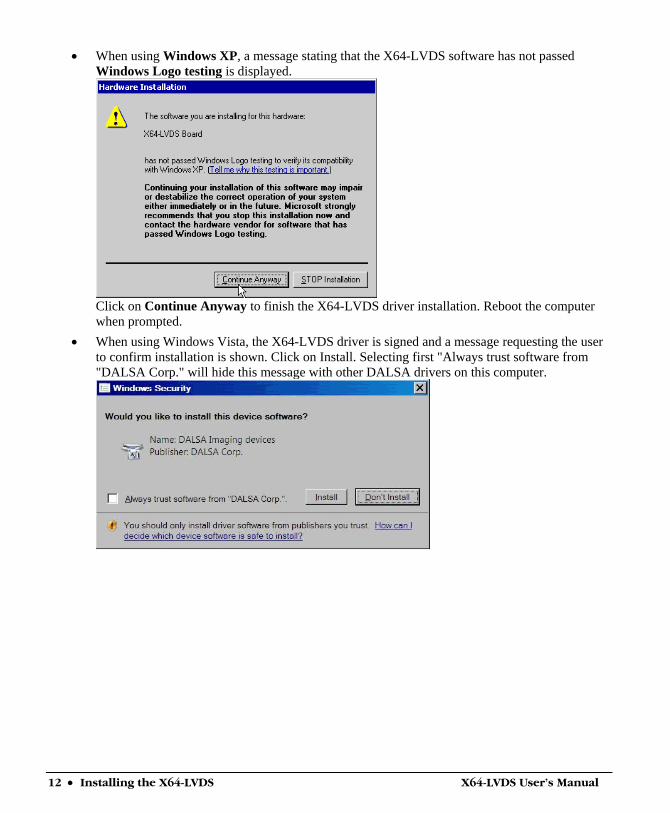
• When using Windows XP, a message stating that the X64-LVDS software has not passed Windows Logo testing is displayed.
Click on Continue Anyway to finish the X64-LVDS driver installation. Reboot the computer when prompted.
• When using Windows Vista, the X64-LVDS driver is signed and a message requesting the user to confirm installation is shown. Click on Install. Selecting first "Always trust software from "DALSA Corp." will hide this message with other DALSA drivers on this computer.
X64-LVDS User's Manual Installing the X64-LVDS • 13
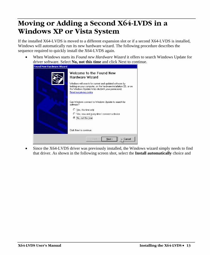
Moving or Adding a Second X64-LVDS in a Windows XP or Vista System If the installed X64-LVDS is moved to a different expansion slot or if a second X64-LVDS is installed, Windows will automatically run its new hardware wizard. The following procedure describes the sequence required to quickly install the X64-LVDS again.
• When Windows starts its Found new Hardware Wizard it offers to search Windows Update for driver software. Select No, not this time and click Next to continue.
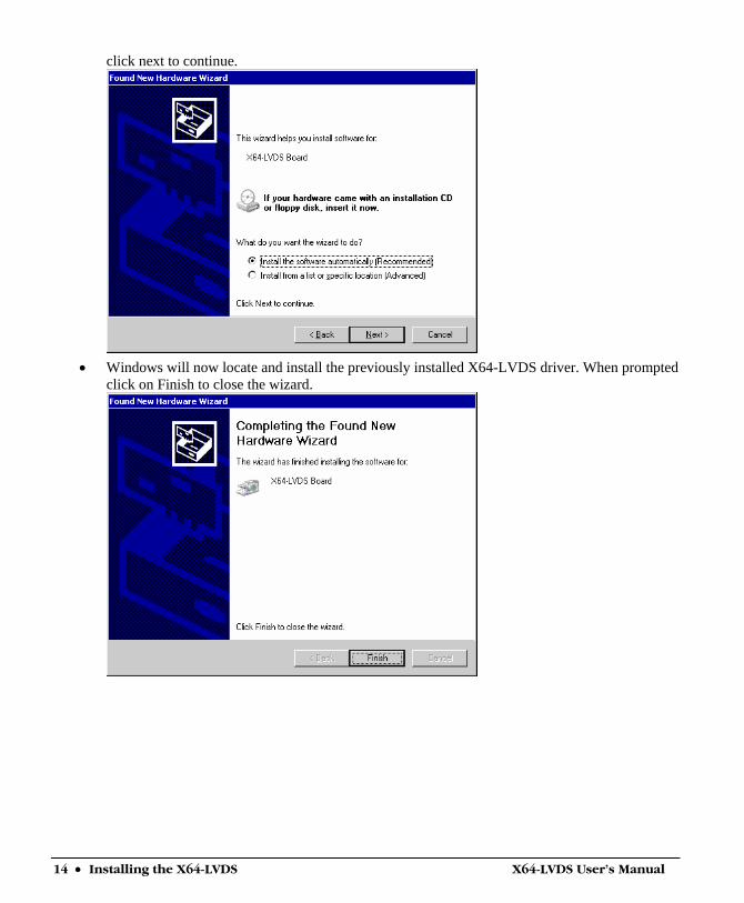
• Since the X64-LVDS driver was previously installed, the Windows wizard simply needs to find
that driver. As shown in the following screen shot, select the Install automatically choice and
14 • Installing the X64-LVDS X64-LVDS User's Manual
click next to continue.
• Windows will now locate and install the previously installed X64-LVDS driver. When prompted
click on Finish to close the wizard.
X64-LVDS User's Manual Installing the X64-LVDS • 15
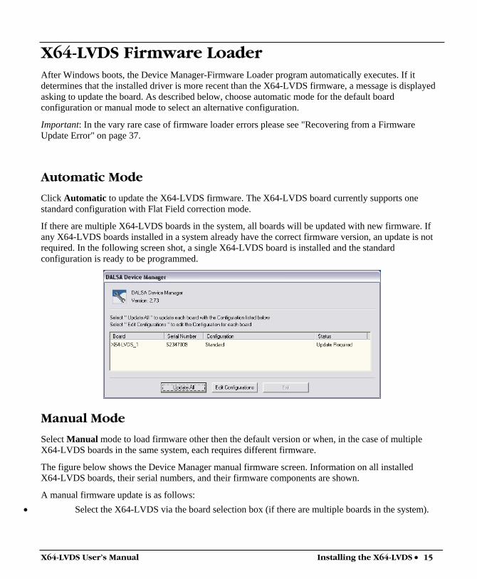
X64-LVDS Firmware Loader After Windows boots, the Device Manager-Firmware Loader program automatically executes. If it determines that the installed driver is more recent than the X64-LVDS firmware, a message is displayed asking to update the board. As described below, choose automatic mode for the default board configuration or manual mode to select an alternative configuration.
Important: In the vary rare case of firmware loader errors please see "Recovering from a Firmware Update Error" on page 37.
Automatic Mode
Click Automatic to update the X64-LVDS firmware. The X64-LVDS board currently supports one standard configuration with Flat Field correction mode.
If there are multiple X64-LVDS boards in the system, all boards will be updated with new firmware. If any X64-LVDS boards installed in a system already have the correct firmware version, an update is not required. In the following screen shot, a single X64-LVDS board is installed and the standard configuration is ready to be programmed.
Manual Mode
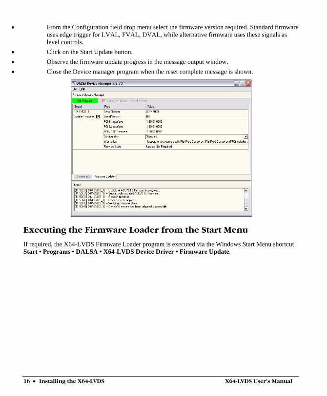
Select Manual mode to load firmware other then the default version or when, in the case of multiple X64-LVDS boards in the same system, each requires different firmware.
The figure below shows the Device Manager manual firmware screen. Information on all installed X64-LVDS boards, their serial numbers, and their firmware components are shown.
A manual firmware update is as follows: • Select the X64-LVDS via the board selection box (if there are multiple boards in the system).
16 • Installing the X64-LVDS X64-LVDS User's Manual
• From the Configuration field drop menu select the firmware version required. Standard firmware uses edge trigger for LVAL, FVAL, DVAL, while alternative firmware uses these signals as level controls.
• Click on the Start Update button. • Observe the firmware update progress in the message output window. • Close the Device manager program when the reset complete message is shown.
Executing the Firmware Loader from the Start Menu
If required, the X64-LVDS Firmware Loader program is executed via the Windows Start Menu shortcut Start • Programs • DALSA • X64-LVDS Device Driver • Firmware Update.
X64-LVDS User's Manual Installing the X64-LVDS • 17
Enabling the Serial Control Port The X64-LVDS includes a serial communication port for direct camera control by the frame grabber. The port is available on the VHDCI J2-Connector 1, where pin-32 is serial out and pin-34 is serial in (see "J2: Dual 68 Pin VHDCI Connectors" on page 82 ). The X64-LVDS driver supports this serial communication port either directly or by mapping it to a host computer COM port. Any serial port communication program, such as Windows HyperTerminal, can connect to the camera in use and modify its function modes via its serial port controls. The X64-LVDS serial port supports communication speeds up to 115 kbps.
Note: if your serial communication program can directly select the X64-LVDS serial port then mapping to a system COM port is not necessary.
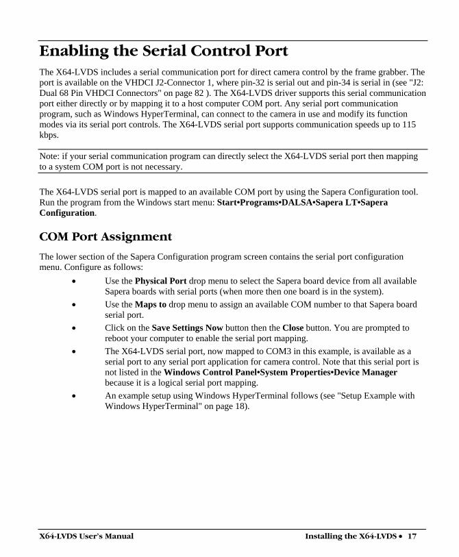
The X64-LVDS serial port is mapped to an available COM port by using the Sapera Configuration tool. Run the program from the Windows start menu: Start•Programs•DALSA•Sapera LT•Sapera Configuration.
COM Port Assignment
The lower section of the Sapera Configuration program screen contains the serial port configuration menu. Configure as follows:
• Use the Physical Port drop menu to select the Sapera board device from all available Sapera boards with serial ports (when more then one board is in the system).
• Use the Maps to drop menu to assign an available COM number to that Sapera board serial port.
• Click on the Save Settings Now button then the Close button. You are prompted to reboot your computer to enable the serial port mapping.
• The X64-LVDS serial port, now mapped to COM3 in this example, is available as a serial port to any serial port application for camera control. Note that this serial port is not listed in the Windows Control Panel•System Properties•Device Manager because it is a logical serial port mapping.
• An example setup using Windows HyperTerminal follows (see "Setup Example with Windows HyperTerminal" on page 18).
18 • Installing the X64-LVDS X64-LVDS User's Manual
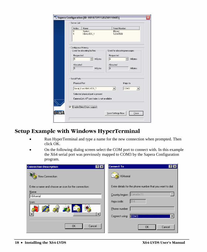
Setup Example with Windows HyperTerminal • Run HyperTerminal and type a name for the new connection when prompted. Then
click OK. • On the following dialog screen select the COM port to connect with. In this example
the X64 serial port was previously mapped to COM3 by the Sapera Configuration program.
X64-LVDS User's Manual Installing the X64-LVDS • 19
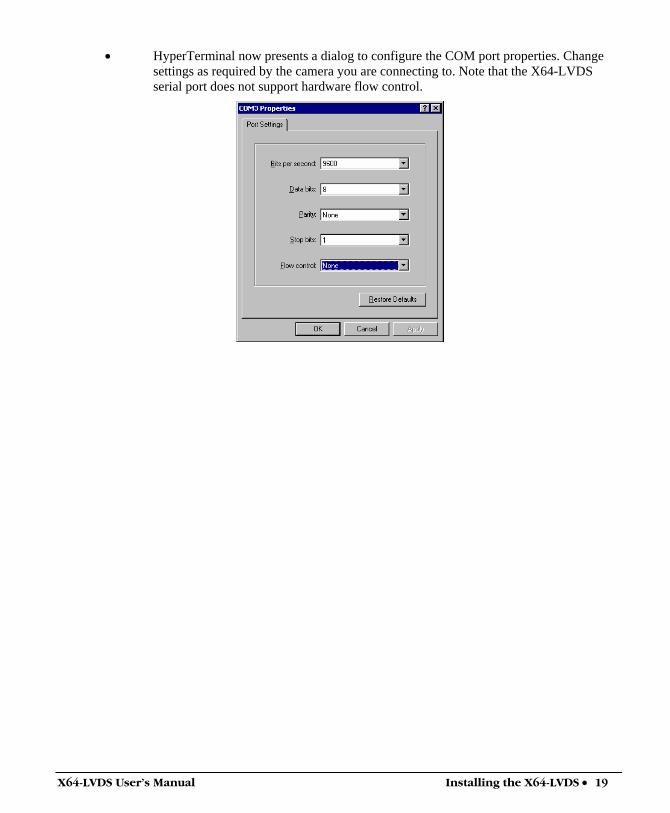
• HyperTerminal now presents a dialog to configure the COM port properties. Change settings as required by the camera you are connecting to. Note that the X64-LVDS serial port does not support hardware flow control.
20 • Installing the X64-LVDS X64-LVDS User's Manual
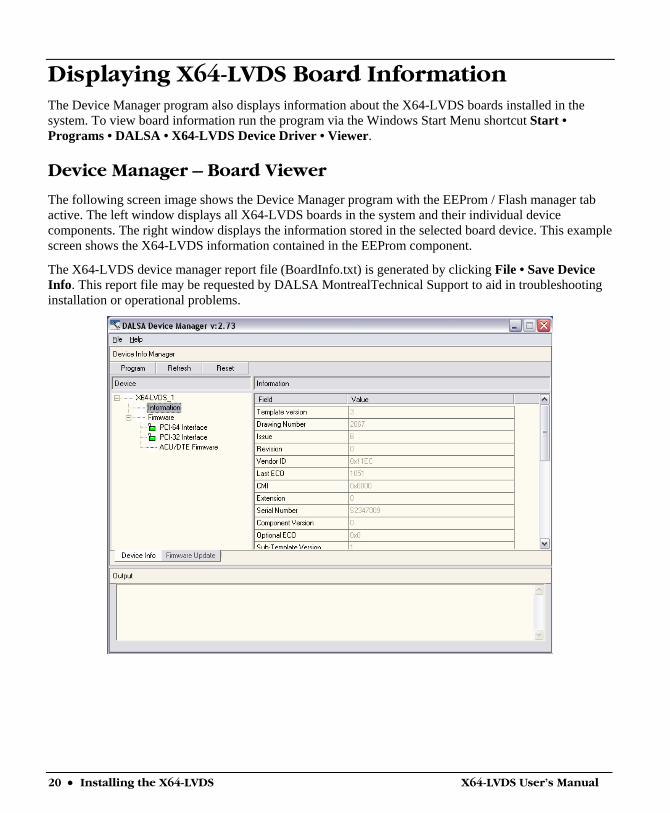
Displaying X64-LVDS Board Information The Device Manager program also displays information about the X64-LVDS boards installed in the system. To view board information run the program via the Windows Start Menu shortcut Start • Programs • DALSA • X64-LVDS Device Driver • Viewer.
Device Manager – Board Viewer
The following screen image shows the Device Manager program with the EEProm / Flash manager tab active. The left window displays all X64-LVDS boards in the system and their individual device components. The right window displays the information stored in the selected board device. This example screen shows the X64-LVDS information contained in the EEProm component.
The X64-LVDS device manager report file (BoardInfo.txt) is generated by clicking File • Save Device Info. This report file may be requested by DALSA MontrealTechnical Support to aid in troubleshooting installation or operational problems.
X64-LVDS User's Manual Installing the X64-LVDS • 21
Configuring Sapera
Viewing Installed Sapera Servers
The Sapera configuration program (Start•Programs•DALSA•Sapera LT•Sapera Configuration) allows the user to see all available Sapera servers for the installed Sapera-compatible boards.
The System entry represents the system server. It corresponds to the host machine (your computer) and is the only server that should always be present. As shown in the following screen image, server index 1 is the X64-LVDS board installed.
Increasing Contiguous Memory for Sapera Resources
The Contiguous Memory section lets the user specify the total amount of contiguous memory (a block of physical memory, occupying consecutive addresses) reserved for the resources needed for Sapera buffers allocation and Sapera messaging. For both items, the Requested value dialog box shows the driver default memory setting while the Allocated value displays the amount of contiguous memory that has been allocated successfully. The default values will generally satisfy the needs of most applications.
The Sapera buffers value determines the total amount of contiguous memory reserved at boot time for the allocation of dynamic resources used for host frame buffer management such as DMA descriptor tables plus other kernel needs. Adjust this value higher if your application generates any out-of-memory

22 • Installing the X64-LVDS X64-LVDS User's Manual
error while allocating host frame buffers. You can approximate the amount of contiguous memory required as follows:
• Calculate the total amount of host memory used for frame buffers ( number of frame buffers • number of pixels per line • number of lines • (2 – if buffer is 10 or 12 bits) ).
• Provide 1MB for every 256 MB of host frame buffer memory required. • Add an additional 1 MB if the frame buffers have a short line length, say 1k or less
( the increased number of individual frame buffers requires more resources ). • Add an additional 2 MB for various static and dynamic Sapera resources. • Test for any memory error when allocating host buffers. Simply use the "General
Options" on page 46 Buffer menu of the Sapera Grab demo program (see "Using the Grab Demo" on page 43) to allocate the number of host buffers required for your acquisition source. Feel free to test the maximum limit of host buffers possible on your host system – the Sapera Grab demo will not crash when the requested number of host frame buffers cannot be allocated.
Host Computer Frame Buffer Memory Limitations
When planning a Sapera application and its host frame buffers used, plus other Sapera memory resources, do not forget the Windows operating system memory needs. Window XP as an example, should always have a minimum of 128 MB for itself.
A Sapera application using scatter gather buffers could consume most of the remaining system memory. When using frame buffers allocated as a single contiguous memory block, typical limitations are one third of the total system memory with a maximum limit of approximately 100 MB. See the "General Options" on page 46 Buffer menu of the Sapera Grab demo program for information on selecting the type of host buffer memory allocation.
Contiguous Memory for Sapera Messaging
The current value for Sapera messaging determines the total amount of contiguous memory reserved at boot time for messages allocation. This memory space is used to store arguments when a Sapera function is called. Increase this value if you are using functions with large arguments, such as arrays and experience any memory errors.
X64-LVDS User's Manual Installing the X64-LVDS • 23
X64-LVDS Camera Connections The following figure shows the connector bracket end view of the X64-LVDS. Refer to section "Connector and Switch Specifications" on page 80 for details on the X64-LVDS connectors. See "J2: Dual 68 Pin VHDCI Connectors" on page 82 and "J1: Dual 68 Pin VHDCI Connectors" on page 90 for a description of the signal pins.
X64-LVDS revision A0 board
Connector 4
Connector 3 Connector 1
Connector 2
LED 1
LED 2
J1 J2
X64-LVDS revision B0 board
Connector 4
Connector 3 Connector 1
Connector 2
LED 1
LED 2
Note: Connector #1 is for camera taps 1 and 2, while connector #2 is for camera taps 3 and 4. Connector #3 is for camera taps 5 and 6, while connector #4 is for camera taps 7 and 8.
The hardware installation process is completed with the connection of a supported camera to the X64-LVDS board. If you purchased the specific cable for your camera from DALSA, the camera and board connectors are labeled on the cable itself. Connect the cable as indicated. If however, you fabricate the cable yourself, contact the DALSA Montreal Camera Application group for information and cable diagrams applicable to your camera.
24 • Installing the X64-LVDS X64-LVDS User's Manual
Camera Connection Examples Overview
The following diagrams are examples of camera connections for the X64-LVDS board. The information presented is generic and does not detail specifics as to camera brand and its signal specifications, or camera cabling requirements. Contact DALSA or browse our web site http://www.imaging.com/camsearch for the latest information on X64-LVDS supported cameras.
The various data input configurations are automatically programmed by the parameters defined in the Sapera camera file loaded for the camera in use. Camera files are easily prepared by the Sapera utility CamExpert.
One Camera – One 8-bit Channel or Tap
bit 0bit 1bit 2bit 3bit 4bit 5bit 6bit 7
Tap 1
bit 0bit 1bit 2bit 3bit 4bit 5bit 6bit 7
X64-LVDS
Camera
Programmable Control Signals
J2 - connectors 1 & 2
LED 1
J8 J9
J1 - connectors 3 & 4
X64-LVDS
J5J3
connector 1 - tap 1
J2: connector 1 - tap 1
If the camera has one channel or tap that outputs 8-bits per pixel:
Connect the camera to the 8-bit data port Tap 1, on the X64-LVDS input connector 1.
X64-LVDS User's Manual Installing the X64-LVDS • 25
One Camera – Two 8-bit Channels or Taps
bit 0bit 1bit 2bit 3bit 4bit 5bit 6bit 7
Tap 1
bit 0bit 1bit 2bit 3bit 4bit 5bit 6bit 7
X64-LVDS
Camera
Programmable Control Signals
J2 - connectors 1 & 2
LED 1
J8 J9
J1 - connectors 3 & 4
X64-LVDS
J5J3
connector 1 - tap 1&2
J2: connector 1 - tap 1
bit 0bit 1bit 2bit 3bit 4bit 5bit 6bit 7
Tap 2
bit 0bit 1bit 2bit 3bit 4bit 5bit 6bit 7
J2: connector 1 - tap 2
If the camera has two channels or taps that output 8-bits per pixel:
Connect the camera channel/tap 1 to the 8-bit data port Tap 1, on the X64-LVDS input connector 1. Connect the camera channel/tap 2 to the 8-bit data port Tap 2, on the X64-LVDS input connector 1.
26 • Installing the X64-LVDS X64-LVDS User's Manual
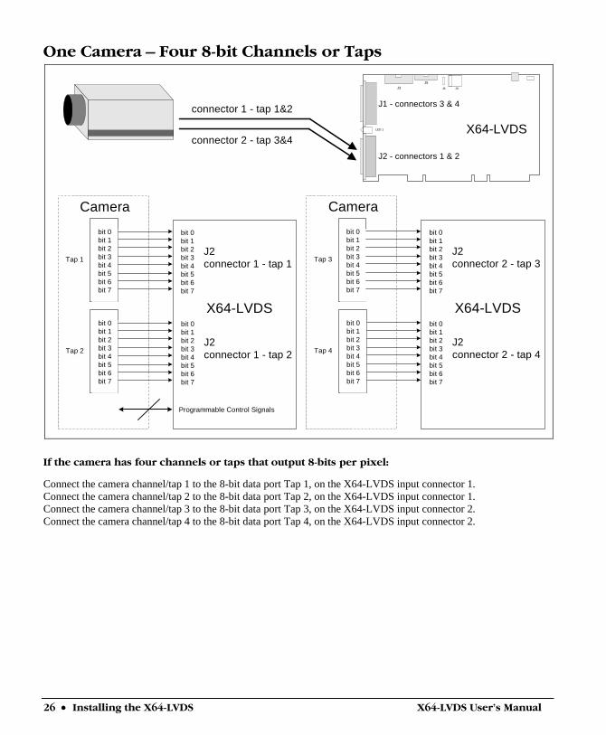
One Camera – Four 8-bit Channels or Taps
J2 - connectors 1 & 2
LED 1
J8 J9
J1 - connectors 3 & 4
X64-LVDS
J5J3
connector 1 - tap 1&2
connector 2 - tap 3&4
bit 0bit 1bit 2bit 3bit 4bit 5bit 6bit 7
Tap 1
bit 0bit 1bit 2bit 3bit 4bit 5bit 6bit 7
X64-LVDS
Camera
Programmable Control Signals
J2connector 1 - tap 1
bit 0bit 1bit 2bit 3bit 4bit 5bit 6bit 7
Tap 2
bit 0bit 1bit 2bit 3bit 4bit 5bit 6bit 7
J2connector 1 - tap 2
bit 0bit 1bit 2bit 3bit 4bit 5bit 6bit 7
Tap 3
bit 0bit 1bit 2bit 3bit 4bit 5bit 6bit 7
X64-LVDS
Camera
J2connector 2 - tap 3
bit 0bit 1bit 2bit 3bit 4bit 5bit 6bit 7
Tap 4
bit 0bit 1bit 2bit 3bit 4bit 5bit 6bit 7
J2connector 2 - tap 4
If the camera has four channels or taps that output 8-bits per pixel:
Connect the camera channel/tap 1 to the 8-bit data port Tap 1, on the X64-LVDS input connector 1. Connect the camera channel/tap 2 to the 8-bit data port Tap 2, on the X64-LVDS input connector 1. Connect the camera channel/tap 3 to the 8-bit data port Tap 3, on the X64-LVDS input connector 2. Connect the camera channel/tap 4 to the 8-bit data port Tap 4, on the X64-LVDS input connector 2.
X64-LVDS User's Manual Installing the X64-LVDS • 27
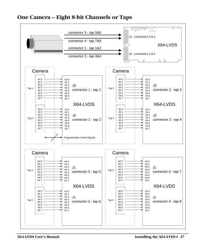
One Camera – Eight 8-bit Channels or Taps
J2 - connectors 1 & 2
LED 1
J8 J9
J1 - connectors 3 & 4
X64-LVDS
J5J3
connector 1 - tap 1&2
connector 2 - tap 3&4
bit 0bit 1bit 2bit 3bit 4bit 5bit 6bit 7
Tap 1
bit 0bit 1bit 2bit 3bit 4bit 5bit 6bit 7
X64-LVDS
Camera
Programmable Control Signals
J2connector 1 - tap 1
bit 0bit 1bit 2bit 3bit 4bit 5bit 6bit 7
Tap 2
bit 0bit 1bit 2bit 3bit 4bit 5bit 6bit 7
J2connector 1 - tap 2
bit 0bit 1bit 2bit 3bit 4bit 5bit 6bit 7
Tap 3
bit 0bit 1bit 2bit 3bit 4bit 5bit 6bit 7
X64-LVDS
Camera
J2connector 2 - tap 3
bit 0bit 1bit 2bit 3bit 4bit 5bit 6bit 7
Tap 4
bit 0bit 1bit 2bit 3bit 4bit 5bit 6bit 7
J2connector 2 - tap 4
connector 3 - tap 5&6
connector 4 - tap 7&8
bit 0bit 1bit 2bit 3bit 4bit 5bit 6bit 7
Tap 1
bit 0bit 1bit 2bit 3bit 4bit 5bit 6bit 7
X64-LVDS
Camera
J1connector 3 - tap 5
bit 0bit 1bit 2bit 3bit 4bit 5bit 6bit 7
Tap 2
bit 0bit 1bit 2bit 3bit 4bit 5bit 6bit 7
J1connector 3 - tap 6
bit 0bit 1bit 2bit 3bit 4bit 5bit 6bit 7
Tap 3
bit 0bit 1bit 2bit 3bit 4bit 5bit 6bit 7
X64-LVDS
Camera
J1connector 4 - tap 7
bit 0bit 1bit 2bit 3bit 4bit 5bit 6bit 7
Tap 4
bit 0bit 1bit 2bit 3bit 4bit 5bit 6bit 7
J1connector 4 - tap 8
28 • Installing the X64-LVDS X64-LVDS User's Manual
If the camera has eight channels or taps that output 8-bits per pixel:
Connect the camera channel/tap 1 to the 8-bit data port Tap 1, on the X64-LVDS input connector 1. Connect the camera channel/tap 2 to the 8-bit data port Tap 2, on the X64-LVDS input connector 1. Connect the camera channel/tap 3 to the 8-bit data port Tap 3, on the X64-LVDS input connector 2. Connect the camera channel/tap 4 to the 8-bit data port Tap 4, on the X64-LVDS input connector 2. Connect the camera channel/tap 5 to the 8-bit data port Tap 5, on the X64-LVDS input connector 3. Connect the camera channel/tap 6 to the 8-bit data port Tap 6, on the X64-LVDS input connector 3. Connect the camera channel/tap 7 to the 8-bit data port Tap 7, on the X64-LVDS input connector 4. Connect the camera channel/tap 8 to the 8-bit data port Tap 8, on the X64-LVDS input connector 4.
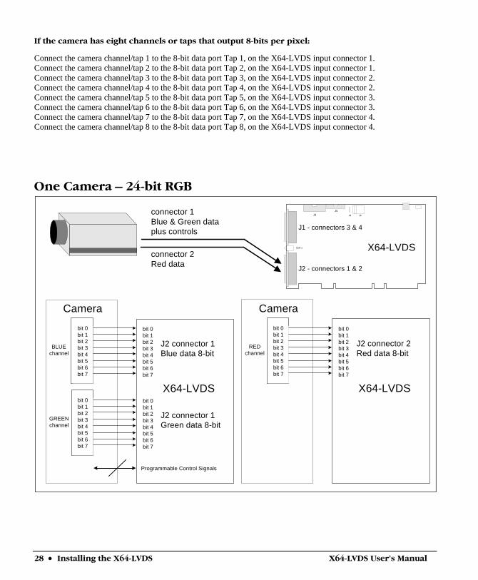
One Camera – 24-bit RGB
J2 - connectors 1 & 2
LED 1
J8 J9
J1 - connectors 3 & 4
X64-LVDS
J5J3connector 1
Blue & Green dataplus controls
connector 2Red data
bit 0bit 1bit 2bit 3bit 4bit 5bit 6bit 7
BLUEchannel
bit 0bit 1bit 2bit 3bit 4bit 5bit 6bit 7
X64-LVDS
Camera
Programmable Control Signals
J2 connector 1Blue data 8-bit
bit 0bit 1bit 2bit 3bit 4bit 5bit 6bit 7
GREENchannel
bit 0bit 1bit 2bit 3bit 4bit 5bit 6bit 7
J2 connector 1Green data 8-bit
bit 0bit 1bit 2bit 3bit 4bit 5bit 6bit 7
REDchannel
bit 0bit 1bit 2bit 3bit 4bit 5bit 6bit 7
X64-LVDS
Camera
J2 connector 2Red data 8-bit
X64-LVDS User's Manual Installing the X64-LVDS • 29
If the camera outputs RGB 24-bit data:
Connect the camera Blue data to X64-LVDS input connector 1. Connect the camera Green data to X64-LVDS input connector 1. Connect the camera Red data to X64-LVDS input connector 2. See "J2 – Connector 1: RGB-24 & RGB-30 Pinout" on page 87 and "J2 – Connector 2: RGB-24 & RGB-30 Pinout" on page 89 for details.
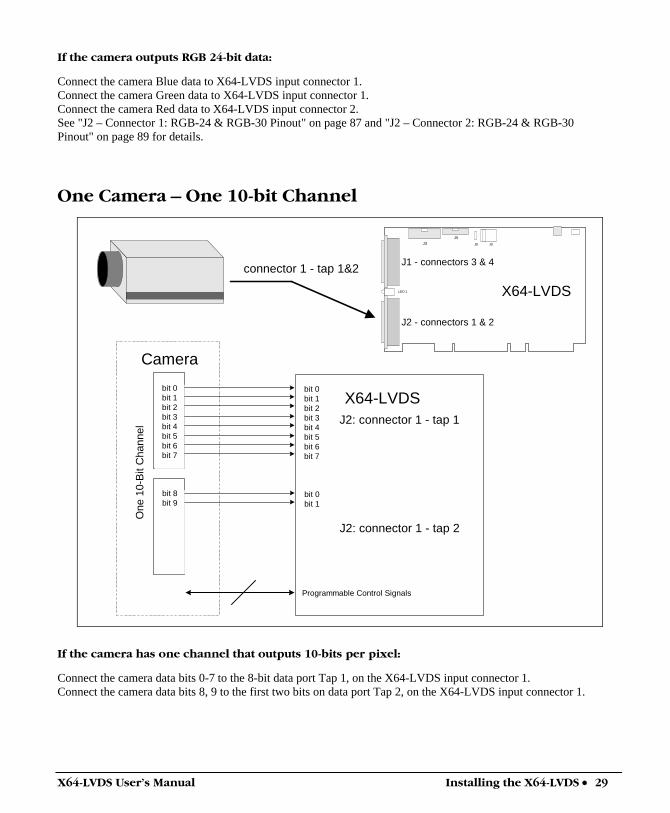
One Camera – One 10-bit Channel
bit 0bit 1bit 2bit 3bit 4bit 5bit 6bit 7
bit 0bit 1bit 2bit 3bit 4bit 5bit 6bit 7
X64-LVDS
Camera
Programmable Control Signals
J2 - connectors 1 & 2
LED 1
J8 J9
J1 - connectors 3 & 4
X64-LVDS
J5J3
connector 1 - tap 1&2
J2: connector 1 - tap 1
bit 8bit 9
One
10-
Bit
Cha
nnel
bit 0bit 1
J2: connector 1 - tap 2
If the camera has one channel that outputs 10-bits per pixel:
Connect the camera data bits 0-7 to the 8-bit data port Tap 1, on the X64-LVDS input connector 1. Connect the camera data bits 8, 9 to the first two bits on data port Tap 2, on the X64-LVDS input connector 1.
30 • Installing the X64-LVDS X64-LVDS User's Manual
One Camera – Two 10-bit Channels
J2 - connectors 1 & 2
LED 1
J8 J9
J1 - connectors 3 & 4
X64-LVDS
J5J3
connector 1 - tap 1&2
connector 2 - tap 3&4
bit 0bit 1bit 2bit 3bit 4bit 5bit 6bit 7
10-b
it C
hann
el #
1
bit 0bit 1bit 2bit 3bit 4bit 5bit 6bit 7
X64-LVDS
Camera
Programmable Control Signals
J2connector 1 - tap 1
bit 8bit 9
bit 0bit 1
J2connector 1 - tap 2
bit 0bit 1bit 2bit 3bit 4bit 5bit 6bit 7
10-b
it C
hann
el #
2
bit 0bit 1bit 2bit 3bit 4bit 5bit 6bit 7
X64-LVDS
Camera
J2connector 2 - tap 3
bit 8bit 9
bit 0bit 1
J2connector 2 - tap 4
If the camera has two channels that output 10-bits per pixel:
Connect the camera channel #1 data bits 0-7 to the 8-bit data port Tap 1, on the X64-LVDS input connector 1. Connect the camera channel #1 data bits 8, 9 to the first two bits on data port Tap 2, on the X64-LVDS input connector 1. Connect the camera channel #2 data bits 0-7 to the 8-bit data port Tap 3, on the X64-LVDS input connector 2. Connect the camera channel #2 data bits 8, 9 to the first two bits on data port Tap 4, on the X64-LVDS input connector 2.
X64-LVDS User's Manual Installing the X64-LVDS • 31
One Camera – Four 10-bit Channels
J2 - connectors 1 & 2
LED 1
J8 J9
J1 - connectors 3 & 4
X64-LVDS
J5J3
connector 1 - tap 1&2
connector 2 - tap 3&4
bit 0bit 1bit 2bit 3bit 4bit 5bit 6bit 7
10-b
it C
hann
el #
1
bit 0bit 1bit 2bit 3bit 4bit 5bit 6bit 7
X64-LVDS
Camera
Programmable Control Signals
J2connector 1 - tap 1
bit 8bit 9
bit 0bit 1
J2connector 1 - tap 2
bit 0bit 1bit 2bit 3bit 4bit 5bit 6bit 7
10-b
it C
hann
el #
2
bit 0bit 1bit 2bit 3bit 4bit 5bit 6bit 7
X64-LVDS
Camera
J2connector 2 - tap 3
bit 8bit 9
bit 0bit 1
J2connector 2 - tap 4
connector 3 - tap 5&6
connector 4 - tap 7&8
bit 0bit 1bit 2bit 3bit 4bit 5bit 6bit 7
10-b
it C
hann
el #
3
bit 0bit 1bit 2bit 3bit 4bit 5bit 6bit 7
X64-LVDS
Camera
J1connector 3 - tap 5
bit 8bit 9
bit 0bit 1
J1connector 3 - tap 6
bit 0bit 1bit 2bit 3bit 4bit 5bit 6bit 7
10-b
it C
hann
el #
4
bit 0bit 1bit 2bit 3bit 4bit 5bit 6bit 7
X64-LVDS
Camera
J1connector 4 - tap 7
bit 8bit 9
bit 0bit 1
J1connector 4 - tap 8
32 • Installing the X64-LVDS X64-LVDS User's Manual
If the camera has four channels that output 10-bits per pixel:
Connect the camera channel #1 data bits 0-7 to the 8-bit data port Tap 1, on the X64-LVDS input connector 1. Connect the camera channel #1 data bits 8, 9 to the first two bits on data port Tap 2, on the X64-LVDS input connector 1. Connect the camera channel #2 data bits 0-7 to the 8-bit data port Tap 3, on the X64-LVDS input connector 2. Connect the camera channel #2 data bits 8, 9 to the first two bits on data port Tap 4, on the X64-LVDS input connector 2. Connect the camera channel #3 data bits 0-7 to the 8-bit data port Tap 5, on the X64-LVDS input connector 3. Connect the camera channel #3 data bits 8, 9 to the first two bits on data port Tap 6, on the X64-LVDS input connector 3. Connect the camera channel #4 data bits 0-7 to the 8-bit data port Tap 7, on the X64-LVDS input connector 4. Connect the camera channel #4 data bits 8, 9 to the first two bits on data port Tap 8, on the X64-LVDS input connector 4.
X64-LVDS User's Manual Installing the X64-LVDS • 33
One Camera – 30-bit RGB
J2 - connectors 1 & 2
LED 1
J8 J9
J1 - connectors 3 & 4
X64-LVDS
J5J3connector 1
Blue & Green dataplus controls
connector 2Green & Red data
bit 0bit 1bit 2bit 3bit 4bit 5bit 6bit 7
X64-LVDS
Camera
Programmable Control Signals
J2 connector 1Blue data
bit 8bit 9
J2 connector 1Green data
bit 6bit 7
X64-LVDS
Camera
J2 connector 2Green databit 8
bit 9
J2 connector 2Red data
Bluechannel
bit 0bit 1bit 2bit 3bit 4bit 5
Greenchannel
Greenchannel
Redchannel
bit 0bit 1bit 2bit 3bit 4bit 5bit 6bit 7bit 8bit 9
If the camera outputs RGB 30-bit data:
Connect the camera Blue data to X64-LVDS input connector 1. Connect the camera Green data (bits 0-5) to X64-LVDS input connector 1. Connect the camera Green data (bits 6-9) to X64-LVDS input connector 2. Connect the camera Red data to X64-LVDS input connector 2. See "J2 – Connector 1: RGB-24 & RGB-30 Pinout" on page 87 and "J2 – Connector 2: RGB-24 & RGB-30 Pinout" on page 89 for details.
34 • Installing the X64-LVDS X64-LVDS User's Manual
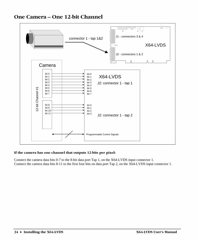
One Camera – One 12-bit Channel
bit 0bit 1bit 2bit 3bit 4bit 5bit 6bit 7
12-b
it C
hann
el #
1
bit 0bit 1bit 2bit 3bit 4bit 5bit 6bit 7
X64-LVDS
Camera
Programmable Control Signals
J2 - connectors 1 & 2
LED 1
J8 J9
J1 - connectors 3 & 4
X64-LVDS
J5J3
connector 1 - tap 1&2
J2: connector 1 - tap 1
bit 8bit 9bit 10bit 11
bit 0bit 1bit 2bit 3 J2: connector 1 - tap 2
If the camera has one channel that outputs 12-bits per pixel:
Connect the camera data bits 0-7 to the 8-bit data port Tap 1, on the X64-LVDS input connector 1. Connect the camera data bits 8-11 to the first four bits on data port Tap 2, on the X64-LVDS input connector 1.
X64-LVDS User's Manual Installing the X64-LVDS • 35
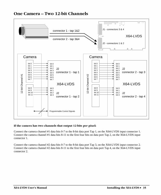
One Camera – Two 12-bit Channels
J2 - connectors 1 & 2
LED 1
J8 J9
J1 - connectors 3 & 4
X64-LVDS
J5J3
connector 1 - tap 1&2
connector 2 - tap 3&4
bit 0bit 1bit 2bit 3bit 4bit 5bit 6bit 7
12-b
it C
hann
el #
1
bit 0bit 1bit 2bit 3bit 4bit 5bit 6bit 7
X64-LVDS
Camera
Programmable Control Signals
J2connector 1 - tap 1
bit 8bit 9bit 10bit 11
bit 0bit 1bit 2bit 3
J2connector 1 - tap 2
bit 0bit 1bit 2bit 3bit 4bit 5bit 6bit 7
12-b
it C
hann
el #
2
bit 0bit 1bit 2bit 3bit 4bit 5bit 6bit 7
X64-LVDS
Camera
J2connector 2 - tap 3
bit 8bit 9bit 10bit 11
bit 0bit 1bit 2bit 3
J2connector 2 - tap 4
If the camera has two channels that output 12-bits per pixel:
Connect the camera channel #1 data bits 0-7 to the 8-bit data port Tap 1, on the X64-LVDS input connector 1. Connect the camera channel #1 data bits 8-11 to the first four bits on data port Tap 2, on the X64-LVDS input connector 1. Connect the camera channel #2 data bits 0-7 to the 8-bit data port Tap 3, on the X64-LVDS input connector 2. Connect the camera channel #2 data bits 8-11 to the first four bits on data port Tap 4, on the X64-LVDS input connector 2.
36 • Installing the X64-LVDS X64-LVDS User's Manual
One Camera – Four 12-bit Channels
J2 - connectors 1 & 2
LED 1
J8 J9
J1 - connectors 3 & 4
X64-LVDS
J5J3
connector 1 - tap 1&2
connector 2 - tap 3&4
bit 0bit 1bit 2bit 3bit 4bit 5bit 6bit 7
12-b
it C
hann
el #
1
bit 0bit 1bit 2bit 3bit 4bit 5bit 6bit 7
X64-LVDS
Camera
Programmable Control Signals
J2connector 1 - tap 1
bit 8bit 9bit 10bit 11
bit 0bit 1bit 2bit 3
J2connector 1 - tap 2
bit 0bit 1bit 2bit 3bit 4bit 5bit 6bit 7
12-b
it C
hann
el #
2
bit 0bit 1bit 2bit 3bit 4bit 5bit 6bit 7
X64-LVDS
Camera
J2connector 2 - tap 3
bit 8bit 9bit 10bit 11
bit 0bit 1bit 2bit 3
J2connector 2 - tap 4
connector 3 - tap 5&6
connector 4 - tap 7&8
bit 0bit 1bit 2bit 3bit 4bit 5bit 6bit 7
12-b
it C
hann
el #
3
bit 0bit 1bit 2bit 3bit 4bit 5bit 6bit 7
X64-LVDS
Camera
J1connector 3 - tap 5
bit 8bit 9bit 10bit 11
bit 0bit 1bit 2bit 3
J1connector 3 - tap 6
bit 0bit 1bit 2bit 3bit 4bit 5bit 6bit 7
12-b
it C
hann
el #
4
bit 0bit 1bit 2bit 3bit 4bit 5bit 6bit 7
X64-LVDS
Camera
J1connector 4 - tap 7
bit 8bit 9bit 10bit 11
bit 0bit 1bit 2bit 3
J1connector 4 - tap 8
X64-LVDS User's Manual Installing the X64-LVDS • 37
If the camera has four channels that output 12-bits per pixel:
Connect the camera channel #1 data bits 0-7 to the 8-bit data port Tap 1, on the X64-LVDS input connector 1. Connect the camera channel #1 data bits 8-11 to the first four bits on data port Tap 2, on the X64-LVDS input connector 1. Connect the camera channel #2 data bits 0-7 to the 8-bit data port Tap 3, on the X64-LVDS input connector 2. Connect the camera channel #2 data bits 8-11 to the first four bits on data port Tap 4, on the X64-LVDS input connector 2. Connect the camera channel #3 data bits 0-7 to the 8-bit data port Tap 5, on the X64-LVDS input connector 3. Connect the camera channel #3 data bits 8-11 to the first four bits on data port Tap 6, on the X64-LVDS input connector 3. Connect the camera channel #4 data bits 0-7 to the 8-bit data port Tap 7, on the X64-LVDS input connector 4. Connect the camera channel #4 data bits 8-11 to the first four bits on data port Tap 8, on the X64-LVDS input connector 4.
Troubleshooting Installation Problems The X64-LVDS (and the X64 family of products) has been tested by DALSA in a wide variety of 64-bit and 32-bit PCI computers. Although unlikely, installation problems may occur. This section describes what the user can check to determine the problem or the checks to make before contacting DALSA Montreal Technical Support.
Recovering from a Firmware Update Error
This procedure is required if any failure occurred while updating the X64-LVDS firmware during installation or during a manual firmware upgrade. On the rare occasion the board has corrupted firmware, any Sapera application such as CamExpert or the grab demo program will not find an installed board to control.
Possible reasons for firmware loading errors or corruption are: • Computer system mains power failure or deep brown-out. • PCI bus or checksum errors. • PCI bus timeout conditions due to other devices. • User forcing a partial firmware upload using an invalid firmware source file.
When the X64-LVDS firmware is corrupted, executing a manual firmware upload will not work because the firmware loader can not communicate with the board. In the extreme case, corrupted firmware may even prevent Windows from booting.
38 • Installing the X64-LVDS X64-LVDS User's Manual
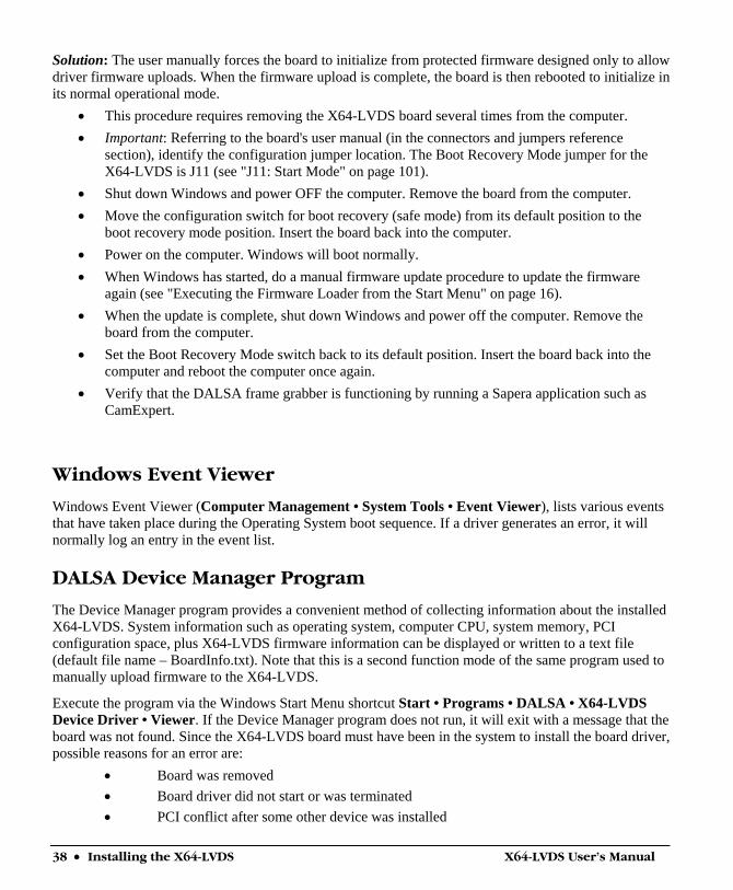
Solution: The user manually forces the board to initialize from protected firmware designed only to allow driver firmware uploads. When the firmware upload is complete, the board is then rebooted to initialize in its normal operational mode.
• This procedure requires removing the X64-LVDS board several times from the computer. • Important: Referring to the board's user manual (in the connectors and jumpers reference
section), identify the configuration jumper location. The Boot Recovery Mode jumper for the X64-LVDS is J11 (see "J11: Start Mode" on page 101).
• Shut down Windows and power OFF the computer. Remove the board from the computer. • Move the configuration switch for boot recovery (safe mode) from its default position to the
boot recovery mode position. Insert the board back into the computer. • Power on the computer. Windows will boot normally. • When Windows has started, do a manual firmware update procedure to update the firmware
again (see "Executing the Firmware Loader from the Start Menu" on page 16). • When the update is complete, shut down Windows and power off the computer. Remove the
board from the computer. • Set the Boot Recovery Mode switch back to its default position. Insert the board back into the
computer and reboot the computer once again. • Verify that the DALSA frame grabber is functioning by running a Sapera application such as
CamExpert.
Windows Event Viewer
Windows Event Viewer (Computer Management • System Tools • Event Viewer), lists various events that have taken place during the Operating System boot sequence. If a driver generates an error, it will normally log an entry in the event list.
DALSA Device Manager Program
The Device Manager program provides a convenient method of collecting information about the installed X64-LVDS. System information such as operating system, computer CPU, system memory, PCI configuration space, plus X64-LVDS firmware information can be displayed or written to a text file (default file name – BoardInfo.txt). Note that this is a second function mode of the same program used to manually upload firmware to the X64-LVDS.
Execute the program via the Windows Start Menu shortcut Start • Programs • DALSA • X64-LVDS Device Driver • Viewer. If the Device Manager program does not run, it will exit with a message that the board was not found. Since the X64-LVDS board must have been in the system to install the board driver, possible reasons for an error are:
• Board was removed • Board driver did not start or was terminated • PCI conflict after some other device was installed
X64-LVDS User's Manual Installing the X64-LVDS • 39
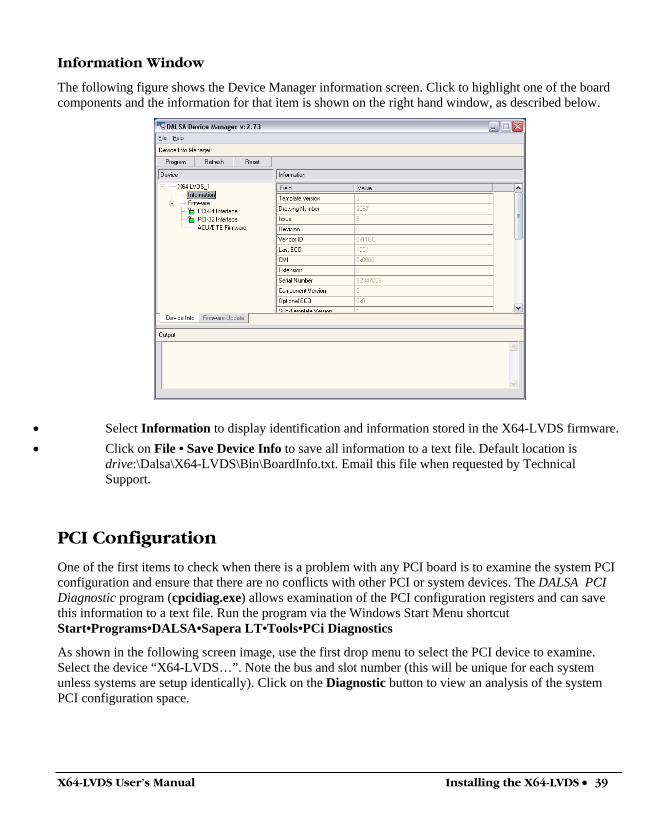
Information Window
The following figure shows the Device Manager information screen. Click to highlight one of the board components and the information for that item is shown on the right hand window, as described below.
• Select Information to display identification and information stored in the X64-LVDS firmware. • Click on File • Save Device Info to save all information to a text file. Default location is
drive:\Dalsa\X64-LVDS\Bin\BoardInfo.txt. Email this file when requested by Technical Support.
PCI Configuration
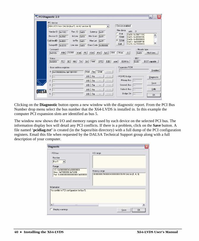
One of the first items to check when there is a problem with any PCI board is to examine the system PCI configuration and ensure that there are no conflicts with other PCI or system devices. The DALSA PCI Diagnostic program (cpcidiag.exe) allows examination of the PCI configuration registers and can save this information to a text file. Run the program via the Windows Start Menu shortcut Start•Programs•DALSA•Sapera LT•Tools•PCi Diagnostics
As shown in the following screen image, use the first drop menu to select the PCI device to examine. Select the device “X64-LVDS…”. Note the bus and slot number (this will be unique for each system unless systems are setup identically). Click on the Diagnostic button to view an analysis of the system PCI configuration space.
40 • Installing the X64-LVDS X64-LVDS User's Manual
Clicking on the Diagnostic button opens a new window with the diagnostic report. From the PCI Bus Number drop menu select the bus number that the X64-LVDS is installed in. In this example the computer PCI expansion slots are identified as bus 5.
The window now shows the I/O and memory ranges used by each device on the selected PCI bus. The information display box will detail any PCI conflicts. If there is a problem, click on the Save button. A file named ‘pcidiag.txt’ is created (in the Sapera\bin directory) with a full dump of the PCI configuration registers. Email this file when requested by the DALSA Technical Support group along with a full description of your computer.
X64-LVDS User's Manual Installing the X64-LVDS • 41
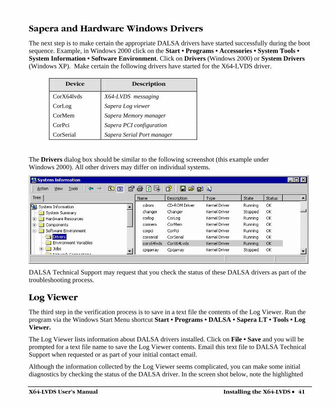
Sapera and Hardware Windows Drivers
The next step is to make certain the appropriate DALSA drivers have started successfully during the boot sequence. Example, in Windows 2000 click on the Start • Programs • Accessories • System Tools • System Information • Software Environment. Click on Drivers (Windows 2000) or System Drivers (Windows XP). Make certain the following drivers have started for the X64-LVDS driver.
Device Description
CorX64lvds X64-LVDS messaging CorLog Sapera Log viewer CorMem Sapera Memory manager CorPci Sapera PCI configuration CorSerial Sapera Serial Port manager
The Drivers dialog box should be similar to the following screenshot (this example under Windows 2000). All other drivers may differ on individual systems.
DALSA Technical Support may request that you check the status of these DALSA drivers as part of the troubleshooting process.
Log Viewer
The third step in the verification process is to save in a text file the contents of the Log Viewer. Run the program via the Windows Start Menu shortcut Start • Programs • DALSA • Sapera LT • Tools • Log Viewer.
The Log Viewer lists information about DALSA drivers installed. Click on File • Save and you will be prompted for a text file name to save the Log Viewer contents. Email this text file to DALSA Technical Support when requested or as part of your initial contact email.
Although the information collected by the Log Viewer seems complicated, you can make some initial diagnostics by checking the status of the DALSA driver. In the screen shot below, note the highlighted
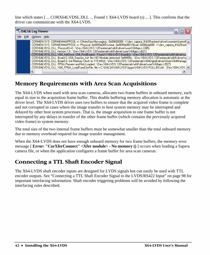
42 • Installing the X64-LVDS X64-LVDS User's Manual
line which states [ ... CORX64LVDSL.DLL ... Found 1 X64-LVDS board (s) ... ]. This confirms that the driver can communicate with the X64-LVDS.
Memory Requirements with Area Scan Acquisitions
The X64-LVDS when used with area scan cameras, allocates two frame buffers in onboard memory, each equal in size to the acquisition frame buffer. This double buffering memory allocation is automatic at the driver level. The X64-LVDS driver uses two buffers to ensure that the acquired video frame is complete and not corrupted in cases where the image transfer to host system memory may be interrupted and delayed by other host system processes. That is, the image acquisition to one frame buffer is not interrupted by any delays in transfer of the other frame buffer (which contains the previously acquired video frame) to system memory.
The total size of the two internal frame buffers must be somewhat smaller than the total onboard memory due to memory overhead required for image transfer management.
When the X64-LVDS does not have enough onboard memory for two frame buffers, the memory error message [ Error: "CorXferConnect" <Xfer module> - No memory () ] occurs when loading a Sapera camera file, or when the application configures a frame buffer for area scan cameras.
Connecting a TTL Shaft Encoder Signal
The X64-LVDS shaft encoder inputs are designed for LVDS signals but can easily be used with TTL encoder outputs. See “Connecting a TTL Shaft Encoder Signal to the LVDS/RS422 Input” on page 98 for important interfacing information. Shaft encoder triggering problems will be avoided by following the interfacing rules described.

X64-LVDS User's Manual The Sapera Demo Application • 43
The Sapera Demo Application
Grab Demo Overview Program Start•Programs•Sapera LT•Demos•Grab Demo Program file \Dalsa\Sapera\Demos\Classes\vc\GrabDemo\Release\GrabDemo.exe Workspace \Dalsa\Sapera\Demos\Classes\vc\SapDemos.dsw Description This program demonstrates the basic acquisition functions included in the Sapera
library. The program allows you to acquire images, either in continuous or in one-shot mode, while adjusting the acquisition parameters. The program code may be extracted for use within your own application.
Remarks This demo is built using Visual C++ 6.0 using the MFC library. It is based on the Sapera standard API and Sapera C++ classes. See the Sapera User’s and Reference manuals for more information.
Using the Grab Demo
Server Selection
Run the grab demo from the start menu Start•Programs•Sapera LT•Demos•Grab Demo.
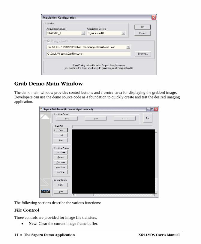
The demo program first displays the acquisition configuration menu. The Acquisition Server drop menu permits selecting from any installed Sapera acquisition servers (installed DALSA acquisition hardware using Sapera drivers). The Acquisition Device drop menu permits selecting from the available input devices available on the selected server.
CCF File Selection
The acquisition configuration menu is also used to select the required camera configuration file for the connected camera. Sapera camera files contain timing parameters and video conditioning parameters. The default folder for camera configuration files is also used by the CamExpert utility to save user generated or modified camera files.
Use the Sapera CamExpert utility program to generate the camera configuration file based on timing and control parameters entered. The CamExpert live acquisition window allows immediate verification of those parameters. CamExpert reads both Sapera *.cca and *.cvi for backward compatibility with the original Sapera camera files.
44 • The Sapera Demo Application X64-LVDS User's Manual
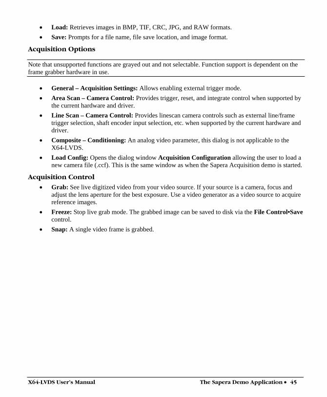
Grab Demo Main Window
The demo main window provides control buttons and a central area for displaying the grabbed image. Developers can use the demo source code as a foundation to quickly create and test the desired imaging application.
The following sections describe the various functions:
File Control
Three controls are provided for image file transfers. • New: Clear the current image frame buffer.
X64-LVDS User's Manual The Sapera Demo Application • 45
• Load: Retrieves images in BMP, TIF, CRC, JPG, and RAW formats. • Save: Prompts for a file name, file save location, and image format.
Acquisition Options
Note that unsupported functions are grayed out and not selectable. Function support is dependent on the frame grabber hardware in use.
• General – Acquisition Settings: Allows enabling external trigger mode. • Area Scan – Camera Control: Provides trigger, reset, and integrate control when supported by
the current hardware and driver. • Line Scan – Camera Control: Provides linescan camera controls such as external line/frame
trigger selection, shaft encoder input selection, etc. when supported by the current hardware and driver.
• Composite – Conditioning: An analog video parameter, this dialog is not applicable to the X64-LVDS.
• Load Config: Opens the dialog window Acquisition Configuration allowing the user to load a new camera file (.ccf). This is the same window as when the Sapera Acquisition demo is started.
Acquisition Control
• Grab: See live digitized video from your video source. If your source is a camera, focus and adjust the lens aperture for the best exposure. Use a video generator as a video source to acquire reference images.
• Freeze: Stop live grab mode. The grabbed image can be saved to disk via the File Control•Save control.
• Snap: A single video frame is grabbed.
46 • The Sapera Demo Application X64-LVDS User's Manual
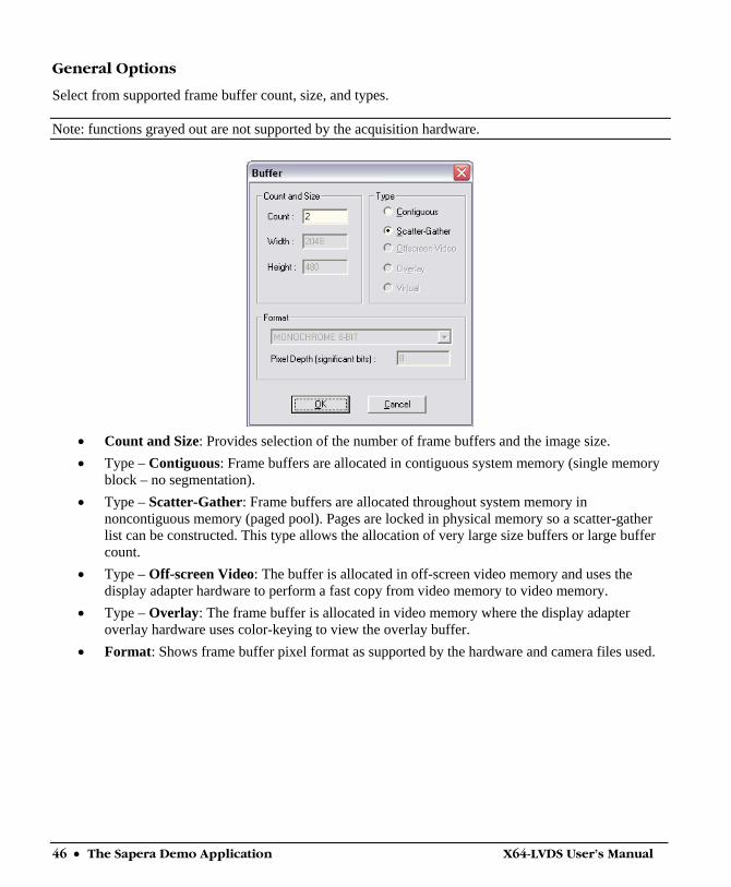
General Options
Select from supported frame buffer count, size, and types.
Note: functions grayed out are not supported by the acquisition hardware.
• Count and Size: Provides selection of the number of frame buffers and the image size. • Type – Contiguous: Frame buffers are allocated in contiguous system memory (single memory
block – no segmentation). • Type – Scatter-Gather: Frame buffers are allocated throughout system memory in
noncontiguous memory (paged pool). Pages are locked in physical memory so a scatter-gather list can be constructed. This type allows the allocation of very large size buffers or large buffer count.
• Type – Off-screen Video: The buffer is allocated in off-screen video memory and uses the display adapter hardware to perform a fast copy from video memory to video memory.
• Type – Overlay: The frame buffer is allocated in video memory where the display adapter overlay hardware uses color-keying to view the overlay buffer.
• Format: Shows frame buffer pixel format as supported by the hardware and camera files used.
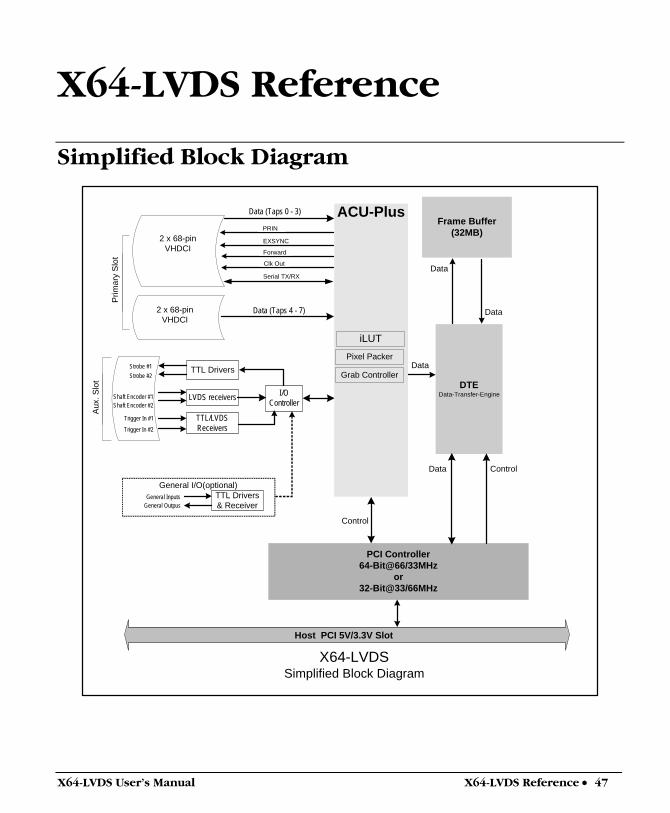
X64-LVDS User's Manual X64-LVDS Reference • 47
X64-LVDS Reference
Simplified Block Diagram
X64-LVDSSimplified Block Diagram
Host PCI 5V/3.3V Slot
TTL Drivers
DTEData-Transfer-Engine
PCI Controller64-Bit@66/33MHz
or32-Bit@33/66MHz
Trigger In #1
Trigger In #2
Strobe #1Strobe #2
Shaft Encoder #1Shaft Encoder #2
LVDS receivers
TTL/LVDSReceivers
I/OController
Data Control
Data
Control
Data
Data
TTL Drivers& Receiver
General InputsGeneral Outpus
General I/O(optional)
2 x 68-pinVHDCI
ACU-Plus
Pixel Packer
Grab Controller
Data (Taps 0 - 3)
Prim
ary
Slo
t
Data (Taps 4 - 7)
Aux.
Slo
t
2 x 68-pinVHDCI
Clk Out
Forward
EXSYNC
PRINFrame Buffer
(32MB)
iLUT
Serial TX/RX
48 • X64-LVDS Reference X64-LVDS User's Manual
X64-LVDS Acquisition Timing
PCLK2
LVAL3
FVAL(Vsync)
Pixel Clock Range: 1Hz up to 75MHz
Min/Max9 HB5
Min/Max4,9 VB6
LVAL/FVAL setup time1
DATA first7 last8
(Hsync)
1 The setup times for LVAL and FVAL are the same. Both must be high and stable before the rising edge of the Pixel Clock.
2 Pixel Clock must always be present. 3 LVAL must be active high to acquire camera data.
For driver 1.10 and later, LVAL and FVAL are edge sensitive. 4 Minimum of 1. 5 HB – Horizontal Blanking:
Minimum: 4 clocks/cycle Maximum: no limits
6 VB – Vertical Blanking: Minimum: 1 line Maximum: no limits
7 First Active Pixel (unless otherwise specified in the CCA file – "Horizontal Back invalid = x" where ‘x’
defines the number of pixels to be skipped). 8 Last Active Pixel – defined in the CCA file under "Horizontal active = y" – where ‘y’ is the total number
of active pixels per tap.
9 Maximum Valid Data: 8-bits/pixel x 256K Pixels/line (LVAL) 16-bits/pixel x 128K Pixels/line (LVAL) 32-bits/pixel x 64K Pixels/line (LVAL) 64-bits/pixel x 32K Pixels/line (LVAL) 16,000,000 lines (FVAL)
X64-LVDS User's Manual X64-LVDS Reference • 49
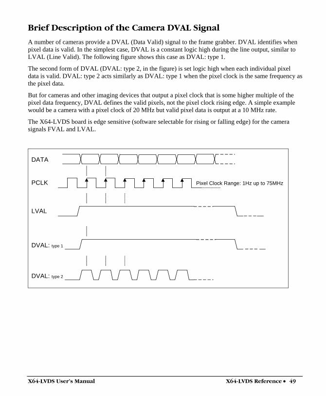
Brief Description of the Camera DVAL Signal
A number of cameras provide a DVAL (Data Valid) signal to the frame grabber. DVAL identifies when pixel data is valid. In the simplest case, DVAL is a constant logic high during the line output, similar to LVAL (Line Valid). The following figure shows this case as DVAL: type 1.
The second form of DVAL (DVAL: type 2, in the figure) is set logic high when each individual pixel data is valid. DVAL: type 2 acts similarly as DVAL: type 1 when the pixel clock is the same frequency as the pixel data.
But for cameras and other imaging devices that output a pixel clock that is some higher multiple of the pixel data frequency, DVAL defines the valid pixels, not the pixel clock rising edge. A simple example would be a camera with a pixel clock of 20 MHz but valid pixel data is output at a 10 MHz rate.
The X64-LVDS board is edge sensitive (software selectable for rising or falling edge) for the camera signals FVAL and LVAL.
PCLK
LVAL
Pixel Clock Range: 1Hz up to 75MHz
DATA
DVAL: type 1
DVAL: type 2
50 • X64-LVDS Reference X64-LVDS User's Manual
Line Trigger Source Selection for Linescan Applications Linescan imaging applications require some form of external event trigger to synchronize linescan camera exposures to the moving object. This synchronization signal is either an external trigger source (one exposure per trigger event) or a shaft encoder source composed of a single or dual phase (quadrature) signal. The X64-LVDS shaft encoder inputs provide additional functionality with pulse drop or pulse multiply support.
The following table describes the line trigger source types supported. Refer to the Sapera Acquisition Parameters Reference Manual (OC-SAPM-APR00) for descriptions of the Sapera parameters.
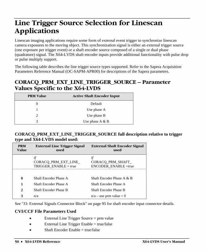
CORACQ_PRM_EXT_LINE_TRIGGER_SOURCE – Parameter Values Specific to the X64-LVDS
PRM Value Active Shaft Encoder Input
0 Default 1 Use phase A 2 Use phase B 3 Use phase A & B
CORACQ_PRM_EXT_LINE_TRIGGER_SOURCE full description relative to trigger type and X64-LVDS model used:
PRM Value
External Line Trigger Signal used
External Shaft Encoder Signal used
if CORACQ_PRM_EXT_LINE_ TRIGGER_ENABLE = true
if CORACQ_PRM_SHAFT_ ENCODER_ENABLE =true
0 Shaft Encoder Phase A Shaft Encoder Phase A & B 1 Shaft Encoder Phase A Shaft Encoder Phase A 2 Shaft Encoder Phase B Shaft Encoder Phase B 3 n/a n/a – use prm value = 0
See "J3: External Signals Connector Block" on page 95 for shaft encoder input connector details.
CVI/CCF File Parameters Used • External Line Trigger Source = prm value • External Line Trigger Enable = true/false • Shaft Encoder Enable = true/false
X64-LVDS User's Manual X64-LVDS Reference • 51
Shaft Encoder Interface Timing Connector J3, Dual Balanced Shaft Encoder Inputs:
• Input 1: Pin 5 (Phase A +) & Pin 6 (Phase A -) (see "J3: External Signals Connector Block" on page 95 for complete connector signal details)
• Input 2: Pin 7 (Phase B +) & Pin 8 (Phase B -) • When using TTL shaft encoders see “Connecting a TTL Shaft Encoder Signal to the
LVDS/RS422 Input” on page 98 for important interfacing information.
Web inspection systems with variable web speeds typically provide one or two synchronization signals from a web mounted encoder to coordinate trigger signals. These trigger signals are used by the acquisition linescan camera. The X64-LVDS supports single or dual shaft encoder signals. Dual encoder signals are typically 90 degrees out of phase relative to each other and provide greater web motion resolution. When using only one shaft encoder input phase, say phase A, then the phase B inputs must be terminated by connecting the + input to a voltage a minimum of 100 mV positive relative to the – input.
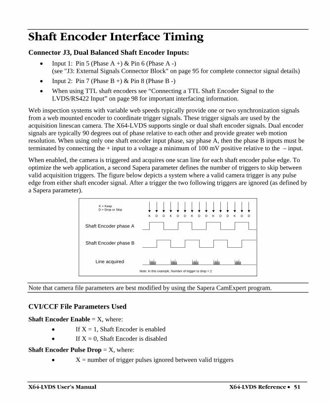
When enabled, the camera is triggered and acquires one scan line for each shaft encoder pulse edge. To optimize the web application, a second Sapera parameter defines the number of triggers to skip between valid acquisition triggers. The figure below depicts a system where a valid camera trigger is any pulse edge from either shaft encoder signal. After a trigger the two following triggers are ignored (as defined by a Sapera parameter).
K D D K D D K D D K D D K D D
Shaft Encoder phase A
Shaft Encoder phase B
K = KeepD = Drop or Skip
Note: in this example, Number of trigger to drop = 2
Line acquired
Note that camera file parameters are best modified by using the Sapera CamExpert program.
CVI/CCF File Parameters Used
Shaft Encoder Enable = X, where: • If X = 1, Shaft Encoder is enabled • If X = 0, Shaft Encoder is disabled
Shaft Encoder Pulse Drop = X, where: • X = number of trigger pulses ignored between valid triggers
52 • X64-LVDS Reference X64-LVDS User's Manual
For information on camera configuration files see the Sapera Acquisition Parameters Reference Manual (OC-SAPM-APR00).
Virtual Frame_Reset for Linescan Cameras When using linescan cameras a frame buffer is allocated in host system memory to store captured video lines. To control when a video line is stored as the first line in this “virtual” frame buffer, an external frame trigger signal called FRAME_RESET is used. The number of lines sequentially grabbed and stored in the virtual frame buffer is controlled by the Sapera vertical cropping parameter.
Virtual Frame_Reset Timing Diagram
The following timing diagram shows an example of grabbing 10 video lines from a linescan camera and the use of FRAME_RESET to define when a video line is stored at the beginning of the virtual frame buffer. The FRAME_RESET signal (generated by some external event) is input on the X64-LVDS trigger input.
• FRAME_RESET can be TTL or LVDS and be rising or falling edge active. • FRAME_RESET control is configured for rising edge trigger in this example. • FRAME_RESET connects to the X64-LVDS via the Trigger In 1 balanced inputs on connector
J3 pin 1 (+) and 2 (-). • After the X64-LVDS receives FRAME_RESET, the EXSYNC control signal is output to the
camera to trigger n lines of video as per the defined virtual frame size. • The EXSYNC control signal is either based on timing controls input on one or both X64-LVDS
shaft encoder inputs (see “J3: External Signals Connector Block” on page 95 pinout) or an internal X64-LVDS clock.
• The number of lines captured is specified by the Sapera vertical cropping parameter.
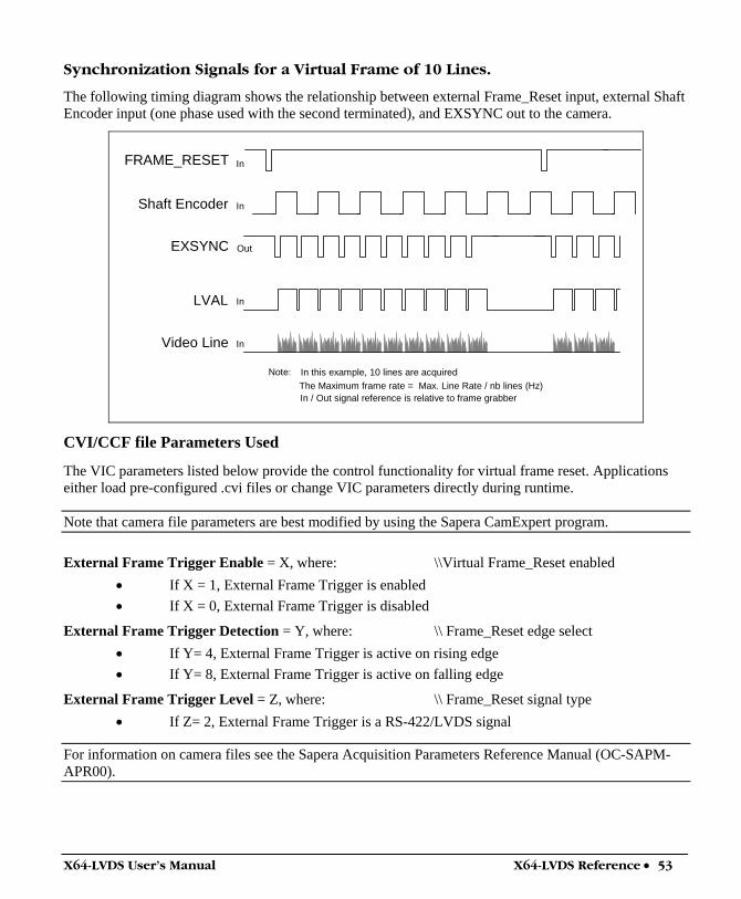
X64-LVDS User's Manual X64-LVDS Reference • 53
Synchronization Signals for a Virtual Frame of 10 Lines.
The following timing diagram shows the relationship between external Frame_Reset input, external Shaft Encoder input (one phase used with the second terminated), and EXSYNC out to the camera.
LVAL
Note: In this example, 10 lines are acquired
Video Line
EXSYNC
The Maximum frame rate = Max. Line Rate / nb lines (Hz)
Shaft Encoder
FRAME_RESET In
In
In
In
Out
In / Out signal reference is relative to frame grabber
CVI/CCF file Parameters Used
The VIC parameters listed below provide the control functionality for virtual frame reset. Applications either load pre-configured .cvi files or change VIC parameters directly during runtime.
Note that camera file parameters are best modified by using the Sapera CamExpert program.
External Frame Trigger Enable = X, where: \\Virtual Frame_Reset enabled • If X = 1, External Frame Trigger is enabled • If X = 0, External Frame Trigger is disabled
External Frame Trigger Detection = Y, where: \\ Frame_Reset edge select • If Y= 4, External Frame Trigger is active on rising edge • If Y= 8, External Frame Trigger is active on falling edge
External Frame Trigger Level = Z, where: \\ Frame_Reset signal type • If Z= 2, External Frame Trigger is a RS-422/LVDS signal
For information on camera files see the Sapera Acquisition Parameters Reference Manual (OC-SAPM-APR00).
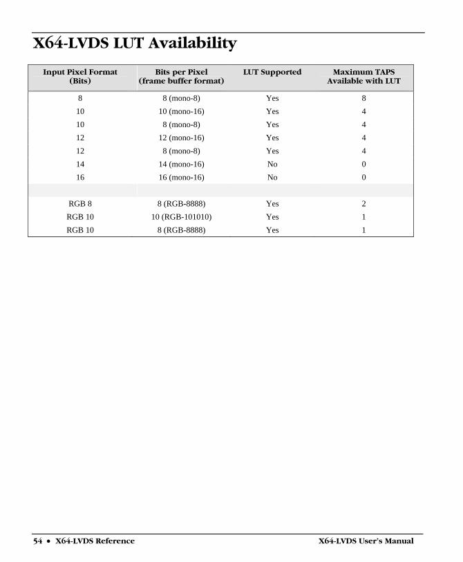
54 • X64-LVDS Reference X64-LVDS User's Manual
X64-LVDS LUT Availability
Input Pixel Format (Bits)
Bits per Pixel (frame buffer format)
LUT Supported Maximum TAPS Available with LUT
8 8 (mono-8) Yes 8 10 10 (mono-16) Yes 4 10 8 (mono-8) Yes 4 12 12 (mono-16) Yes 4 12 8 (mono-8) Yes 4 14 14 (mono-16) No 0 16 16 (mono-16) No 0
RGB 8 8 (RGB-8888) Yes 2 RGB 10 10 (RGB-101010) Yes 1 RGB 10 8 (RGB-8888) Yes 1
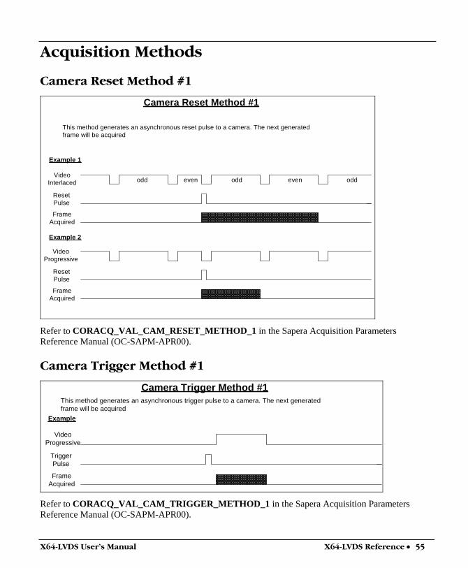
X64-LVDS User's Manual X64-LVDS Reference • 55
Acquisition Methods
Camera Reset Method #1
Camera Reset Method #1
VideoInterlaced oddeven
ResetPulse
VideoProgressive
odd
FrameAcquired
ResetPulse
FrameAcquired
This method generates an asynchronous reset pulse to a camera. The next generatedframe will be acquired
Example 1
Example 2
even odd
Refer to CORACQ_VAL_CAM_RESET_METHOD_1 in the Sapera Acquisition Parameters Reference Manual (OC-SAPM-APR00).
Camera Trigger Method #1
Camera Trigger Method #1
VideoProgressive
TriggerPulse
FrameAcquired
This method generates an asynchronous trigger pulse to a camera. The next generatedframe will be acquired
Example
Refer to CORACQ_VAL_CAM_TRIGGER_METHOD_1 in the Sapera Acquisition Parameters Reference Manual (OC-SAPM-APR00).
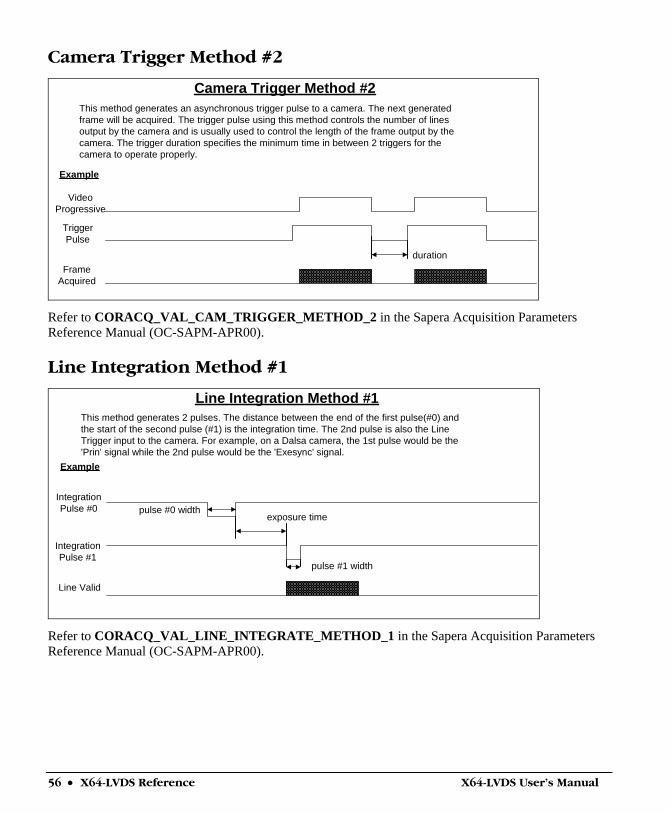
56 • X64-LVDS Reference X64-LVDS User's Manual
Camera Trigger Method #2
Camera Trigger Method #2
VideoProgressive
TriggerPulse
FrameAcquired
This method generates an asynchronous trigger pulse to a camera. The next generatedframe will be acquired. The trigger pulse using this method controls the number of linesoutput by the camera and is usually used to control the length of the frame output by thecamera. The trigger duration specifies the minimum time in between 2 triggers for thecamera to operate properly.
Example
duration
Refer to CORACQ_VAL_CAM_TRIGGER_METHOD_2 in the Sapera Acquisition Parameters Reference Manual (OC-SAPM-APR00).
Line Integration Method #1
Line Integration Method #1
IntegrationPulse #1
Line Valid
This method generates 2 pulses. The distance between the end of the first pulse(#0) andthe start of the second pulse (#1) is the integration time. The 2nd pulse is also the LineTrigger input to the camera. For example, on a Dalsa camera, the 1st pulse would be the'Prin' signal while the 2nd pulse would be the 'Exesync' signal.
Example
exposure time
IntegrationPulse #0
pulse #1 width
pulse #0 width
Refer to CORACQ_VAL_LINE_INTEGRATE_METHOD_1 in the Sapera Acquisition Parameters Reference Manual (OC-SAPM-APR00).
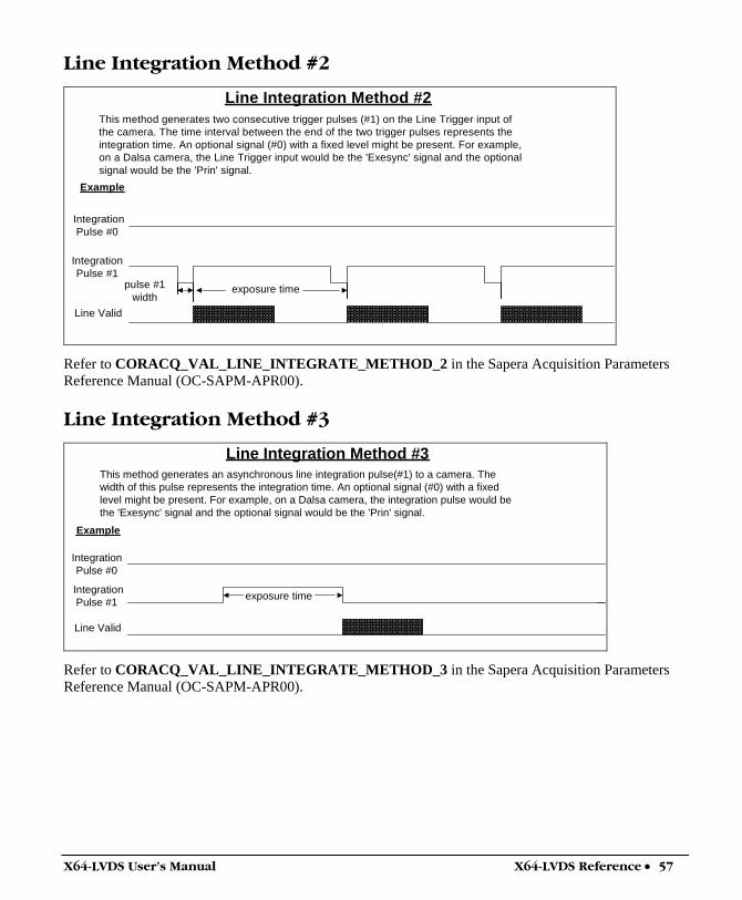
X64-LVDS User's Manual X64-LVDS Reference • 57
Line Integration Method #2
Line Integration Method #2
IntegrationPulse #1
Line Valid
This method generates two consecutive trigger pulses (#1) on the Line Trigger input ofthe camera. The time interval between the end of the two trigger pulses represents theintegration time. An optional signal (#0) with a fixed level might be present. For example,on a Dalsa camera, the Line Trigger input would be the 'Exesync' signal and the optionalsignal would be the 'Prin' signal.
Example
exposure timepulse #1width
IntegrationPulse #0
Refer to CORACQ_VAL_LINE_INTEGRATE_METHOD_2 in the Sapera Acquisition Parameters Reference Manual (OC-SAPM-APR00).
Line Integration Method #3
Line Integration Method #3
IntegrationPulse #0
Line Valid
This method generates an asynchronous line integration pulse(#1) to a camera. Thewidth of this pulse represents the integration time. An optional signal (#0) with a fixedlevel might be present. For example, on a Dalsa camera, the integration pulse would bethe 'Exesync' signal and the optional signal would be the 'Prin' signal.
Example
exposure time IntegrationPulse #1
Refer to CORACQ_VAL_LINE_INTEGRATE_METHOD_3 in the Sapera Acquisition Parameters Reference Manual (OC-SAPM-APR00).
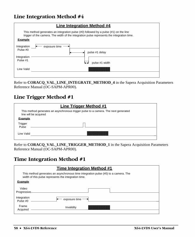
58 • X64-LVDS Reference X64-LVDS User's Manual
Line Integration Method #4
Line Integration Method #4
IntegrationPulse #1
Line Valid
This method generates an integration pulse (#0) followed by a pulse (#1) on the linetrigger of the camera. The width of the integration pulse represents the integration time.
Example
exposure timeIntegrationPulse #0
pulse #1 delay
pulse #1 width
Refer to CORACQ_VAL_LINE_INTEGRATE_METHOD_4 in the Sapera Acquisition Parameters Reference Manual (OC-SAPM-APR00).
Line Trigger Method #1
Line Trigger Method #1
TriggerPulse
Line Valid
This method generates an asynchronous trigger pulse to a camera. The next generatedline will be acquired
Example
Refer to CORACQ_VAL_LINE_TRIGGER_METHOD_1 in the Sapera Acquisition Parameters Reference Manual (OC-SAPM-APR00).
Time Integration Method #1
Time Integration Method #1
VideoProgressive
IntegrationPulse #0
FrameAcquired
This method generates an asynchronous time integration pulse (#0) to a camera. Thewidth of this pulse represents the integration time.
Example
exposure time
Invalidity
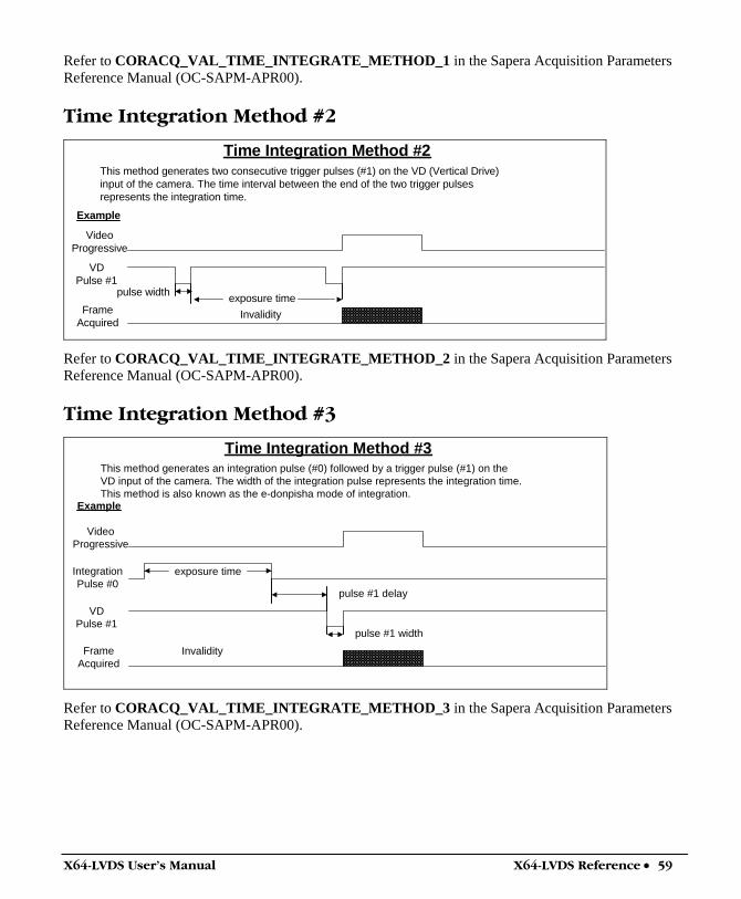
X64-LVDS User's Manual X64-LVDS Reference • 59
Refer to CORACQ_VAL_TIME_INTEGRATE_METHOD_1 in the Sapera Acquisition Parameters Reference Manual (OC-SAPM-APR00).
Time Integration Method #2
Time Integration Method #2
VideoProgressive
VDPulse #1
FrameAcquired
This method generates two consecutive trigger pulses (#1) on the VD (Vertical Drive)input of the camera. The time interval between the end of the two trigger pulsesrepresents the integration time.
Example
exposure timepulse width
Invalidity
Refer to CORACQ_VAL_TIME_INTEGRATE_METHOD_2 in the Sapera Acquisition Parameters Reference Manual (OC-SAPM-APR00).
Time Integration Method #3
Time Integration Method #3
VideoProgressive
VDPulse #1
FrameAcquired
This method generates an integration pulse (#0) followed by a trigger pulse (#1) on theVD input of the camera. The width of the integration pulse represents the integration time.This method is also known as the e-donpisha mode of integration.
Example
exposure timeIntegrationPulse #0
pulse #1 delay
pulse #1 width
Invalidity
Refer to CORACQ_VAL_TIME_INTEGRATE_METHOD_3 in the Sapera Acquisition Parameters Reference Manual (OC-SAPM-APR00).
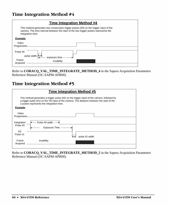
60 • X64-LVDS Reference X64-LVDS User's Manual
Time Integration Method #4
Time Integration Method #4
VideoProgressive
Pulse #0
FrameAcquired
This method generates two consecutive trigger pulses (#0) on the trigger input of thecamera. The time interval between the start of the two trigger pulses represents theintegration time.
Example
exposure timepulse width
Invalidity
Refer to CORACQ_VAL_TIME_INTEGRATE_METHOD_4 in the Sapera Acquisition Parameters Reference Manual (OC-SAPM-APR00).
Time Integration Method #5
Time Integration Method #5
VideoProgressive
VDPulse #1
FrameAcquired
This method generates a trigger pulse (#0) on the trigger input of the camera, followed bya trigger pulse (#1) on the VD input of the camera. The distance between the start of the2 pulses represents the integration time.
Example
Pulse #0 widthIntegrationPulse #0
pulse #1 widthInvalidity
Exposure Time
Refer to CORACQ_VAL_TIME_INTEGRATE_METHOD_5 in the Sapera Acquisition Parameters Reference Manual (OC-SAPM-APR00).
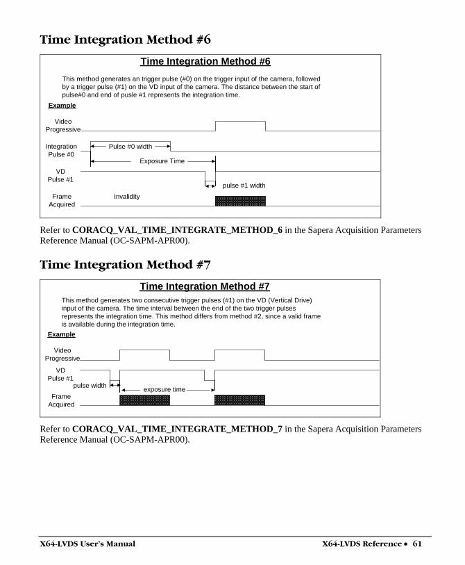
X64-LVDS User's Manual X64-LVDS Reference • 61
Time Integration Method #6
Time Integration Method #6
VideoProgressive
VDPulse #1
FrameAcquired
This method generates an trigger pulse (#0) on the trigger input of the camera, followedby a trigger pulse (#1) on the VD input of the camera. The distance between the start ofpulse#0 and end of pusle #1 represents the integration time.
Example
Pulse #0 widthIntegrationPulse #0
pulse #1 widthInvalidity
Exposure Time
Refer to CORACQ_VAL_TIME_INTEGRATE_METHOD_6 in the Sapera Acquisition Parameters Reference Manual (OC-SAPM-APR00).
Time Integration Method #7
Time Integration Method #7
VideoProgressive
VDPulse #1
FrameAcquired
This method generates two consecutive trigger pulses (#1) on the VD (Vertical Drive)input of the camera. The time interval between the end of the two trigger pulsesrepresents the integration time. This method differs from method #2, since a valid frameis available during the integration time.
Example
exposure timepulse width
Refer to CORACQ_VAL_TIME_INTEGRATE_METHOD_7 in the Sapera Acquisition Parameters Reference Manual (OC-SAPM-APR00).
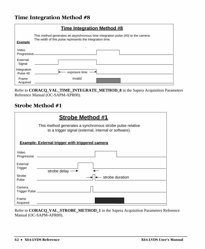
62 • X64-LVDS Reference X64-LVDS User's Manual
Time Integration Method #8
Time Integration Method #8
VideoProgressive
IntegrationPulse #0
FrameAcquired
This method generates an asynchronous time integration pulse (#0) to the camera.The width of this pulse represents the integration time.
Example
ExternalSignal
Invalid
exposure time
Refer to CORACQ_VAL_TIME_INTEGRATE_METHOD_8 in the Sapera Acquisition Parameters Reference Manual (OC-SAPM-APR00).
Strobe Method #1
Strobe Method #1This method generates a synchronous strobe pulse relative
to a trigger signal (external, internal or software).
Example: External trigger with triggered camera
VideoProgressive
CameraTrigger Pulse
FrameAcquired
StrobePulse
strobe delay
ExternalTrigger
strobe duration
Refer to CORACQ_VAL_STROBE_METHOD_1 in the Sapera Acquisition Parameters Reference Manual (OC-SAPM-APR00).
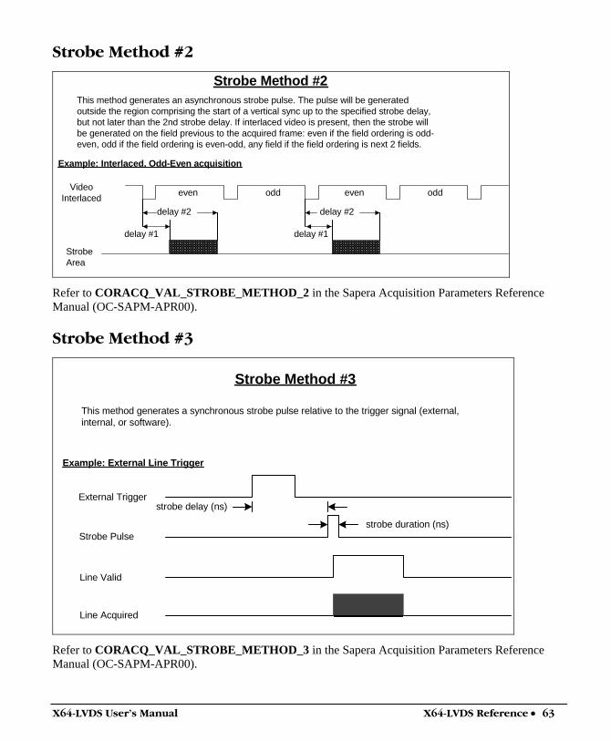
X64-LVDS User's Manual X64-LVDS Reference • 63
Strobe Method #2
Strobe Method #2This method generates an asynchronous strobe pulse. The pulse will be generatedoutside the region comprising the start of a vertical sync up to the specified strobe delay,but not later than the 2nd strobe delay. If interlaced video is present, then the strobe willbe generated on the field previous to the acquired frame: even if the field ordering is odd-even, odd if the field ordering is even-odd, any field if the field ordering is next 2 fields.
Example: Interlaced, Odd-Even acquisition
VideoInterlaced even evenodd odd
StrobeArea
delay #2
delay #1
delay #2
delay #1
Refer to CORACQ_VAL_STROBE_METHOD_2 in the Sapera Acquisition Parameters Reference Manual (OC-SAPM-APR00).
Strobe Method #3
Strobe Method #3
This method generates a synchronous strobe pulse relative to the trigger signal (external,internal, or software).
Example: External Line Trigger
External Trigger
Strobe Pulse
Line Valid
Line Acquired
strobe delay (ns)
strobe duration (ns)
Refer to CORACQ_VAL_STROBE_METHOD_3 in the Sapera Acquisition Parameters Reference Manual (OC-SAPM-APR00).
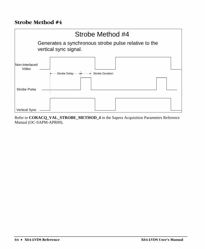
64 • X64-LVDS Reference X64-LVDS User's Manual
Strobe Method #4
Strobe Delay Strobe Duration
Non-InterlacedVideo
Strobe Pulse
Vertical Sync
Strobe Method #4Generates a synchronous strobe pulse relative to thevertical sync signal.
Refer to CORACQ_VAL_STROBE_METHOD_4 in the Sapera Acquisition Parameters Reference Manual (OC-SAPM-APR00).
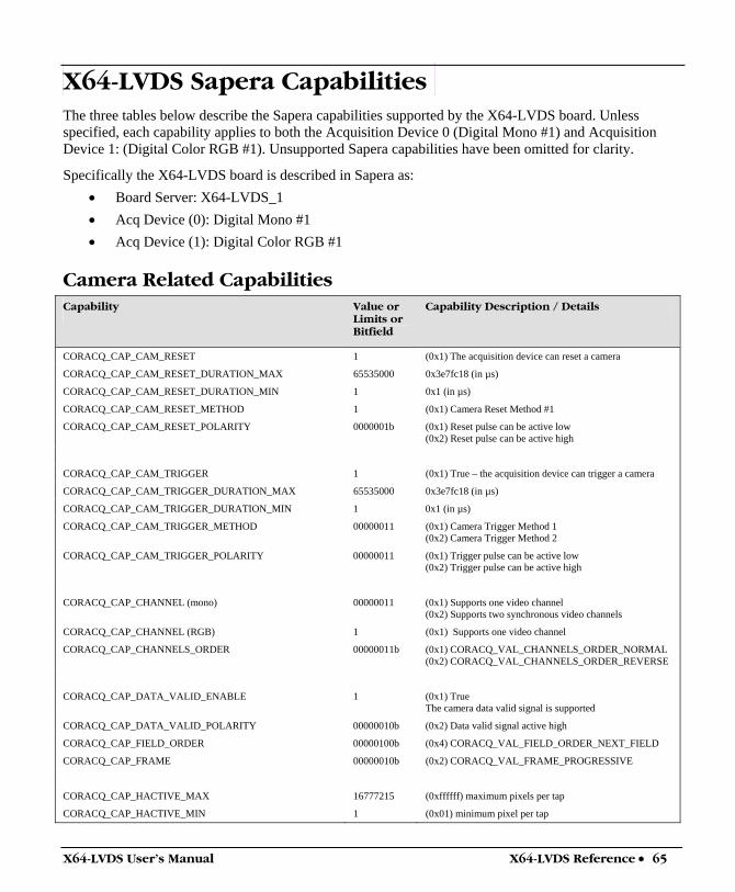
X64-LVDS User's Manual X64-LVDS Reference • 65
X64-LVDS Sapera Capabilities The three tables below describe the Sapera capabilities supported by the X64-LVDS board. Unless specified, each capability applies to both the Acquisition Device 0 (Digital Mono #1) and Acquisition Device 1: (Digital Color RGB #1). Unsupported Sapera capabilities have been omitted for clarity.
Specifically the X64-LVDS board is described in Sapera as: • Board Server: X64-LVDS_1 • Acq Device (0): Digital Mono #1 • Acq Device (1): Digital Color RGB #1
Camera Related Capabilities Capability Value or
Limits or Bitfield
Capability Description / Details
CORACQ_CAP_CAM_RESET 1 (0x1) The acquisition device can reset a camera
CORACQ_CAP_CAM_RESET_DURATION_MAX 65535000 0x3e7fc18 (in µs)
CORACQ_CAP_CAM_RESET_DURATION_MIN 1 0x1 (in µs)
CORACQ_CAP_CAM_RESET_METHOD 1 (0x1) Camera Reset Method #1
CORACQ_CAP_CAM_RESET_POLARITY 0000001b (0x1) Reset pulse can be active low (0x2) Reset pulse can be active high
CORACQ_CAP_CAM_TRIGGER 1 (0x1) True – the acquisition device can trigger a camera
CORACQ_CAP_CAM_TRIGGER_DURATION_MAX 65535000 0x3e7fc18 (in µs)
CORACQ_CAP_CAM_TRIGGER_DURATION_MIN 1 0x1 (in µs)
CORACQ_CAP_CAM_TRIGGER_METHOD 00000011 (0x1) Camera Trigger Method 1 (0x2) Camera Trigger Method 2
CORACQ_CAP_CAM_TRIGGER_POLARITY 00000011 (0x1) Trigger pulse can be active low (0x2) Trigger pulse can be active high
CORACQ_CAP_CHANNEL (mono) 00000011 (0x1) Supports one video channel (0x2) Supports two synchronous video channels
CORACQ_CAP_CHANNEL (RGB) 1 (0x1) Supports one video channel
CORACQ_CAP_CHANNELS_ORDER 00000011b (0x1) CORACQ_VAL_CHANNELS_ORDER_NORMAL (0x2) CORACQ_VAL_CHANNELS_ORDER_REVERSE
CORACQ_CAP_DATA_VALID_ENABLE 1 (0x1) True The camera data valid signal is supported
CORACQ_CAP_DATA_VALID_POLARITY 00000010b (0x2) Data valid signal active high
CORACQ_CAP_FIELD_ORDER 00000100b (0x4) CORACQ_VAL_FIELD_ORDER_NEXT_FIELD
CORACQ_CAP_FRAME 00000010b (0x2) CORACQ_VAL_FRAME_PROGRESSIVE
CORACQ_CAP_HACTIVE_MAX 16777215 (0xffffff) maximum pixels per tap
CORACQ_CAP_HACTIVE_MIN 1 (0x01) minimum pixel per tap
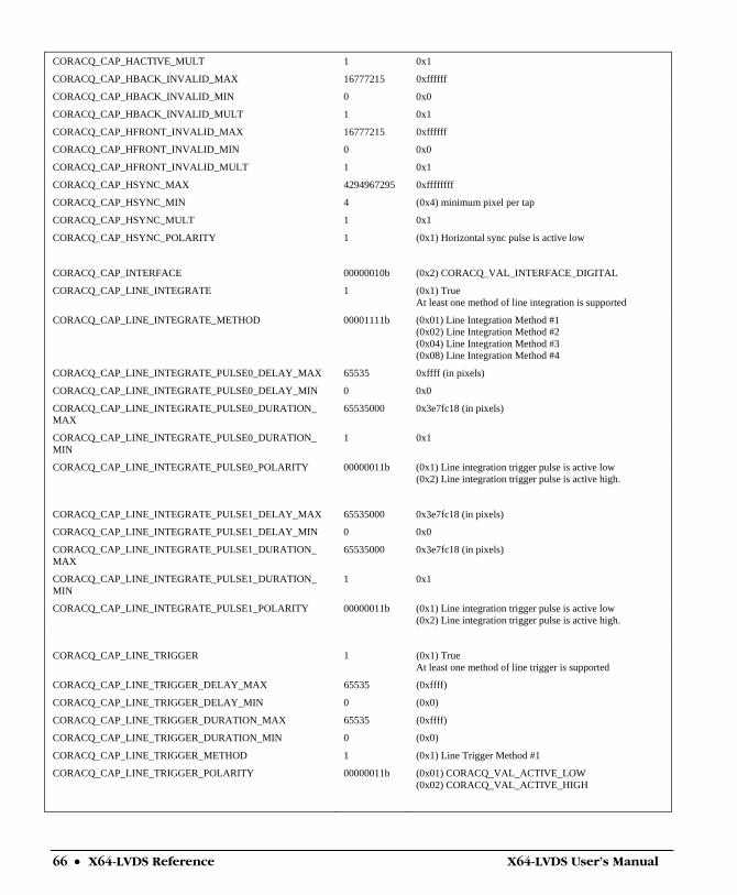
66 • X64-LVDS Reference X64-LVDS User's Manual
CORACQ_CAP_HACTIVE_MULT 1 0x1
CORACQ_CAP_HBACK_INVALID_MAX 16777215 0xffffff
CORACQ_CAP_HBACK_INVALID_MIN 0 0x0
CORACQ_CAP_HBACK_INVALID_MULT 1 0x1
CORACQ_CAP_HFRONT_INVALID_MAX 16777215 0xffffff
CORACQ_CAP_HFRONT_INVALID_MIN 0 0x0
CORACQ_CAP_HFRONT_INVALID_MULT 1 0x1
CORACQ_CAP_HSYNC_MAX 4294967295 0xffffffff
CORACQ_CAP_HSYNC_MIN 4 (0x4) minimum pixel per tap
CORACQ_CAP_HSYNC_MULT 1 0x1
CORACQ_CAP_HSYNC_POLARITY 1 (0x1) Horizontal sync pulse is active low
CORACQ_CAP_INTERFACE 00000010b (0x2) CORACQ_VAL_INTERFACE_DIGITAL
CORACQ_CAP_LINE_INTEGRATE 1 (0x1) True At least one method of line integration is supported
CORACQ_CAP_LINE_INTEGRATE_METHOD 00001111b (0x01) Line Integration Method #1 (0x02) Line Integration Method #2 (0x04) Line Integration Method #3 (0x08) Line Integration Method #4
CORACQ_CAP_LINE_INTEGRATE_PULSE0_DELAY_MAX 65535 0xffff (in pixels)
CORACQ_CAP_LINE_INTEGRATE_PULSE0_DELAY_MIN 0 0x0
CORACQ_CAP_LINE_INTEGRATE_PULSE0_DURATION_ MAX
65535000 0x3e7fc18 (in pixels)
CORACQ_CAP_LINE_INTEGRATE_PULSE0_DURATION_ MIN
1 0x1
CORACQ_CAP_LINE_INTEGRATE_PULSE0_POLARITY 00000011b (0x1) Line integration trigger pulse is active low (0x2) Line integration trigger pulse is active high.
CORACQ_CAP_LINE_INTEGRATE_PULSE1_DELAY_MAX 65535000 0x3e7fc18 (in pixels)
CORACQ_CAP_LINE_INTEGRATE_PULSE1_DELAY_MIN 0 0x0
CORACQ_CAP_LINE_INTEGRATE_PULSE1_DURATION_ MAX
65535000 0x3e7fc18 (in pixels)
CORACQ_CAP_LINE_INTEGRATE_PULSE1_DURATION_ MIN
1 0x1
CORACQ_CAP_LINE_INTEGRATE_PULSE1_POLARITY 00000011b (0x1) Line integration trigger pulse is active low (0x2) Line integration trigger pulse is active high.
CORACQ_CAP_LINE_TRIGGER 1 (0x1) True At least one method of line trigger is supported
CORACQ_CAP_LINE_TRIGGER_DELAY_MAX 65535 (0xffff)
CORACQ_CAP_LINE_TRIGGER_DELAY_MIN 0 (0x0)
CORACQ_CAP_LINE_TRIGGER_DURATION_MAX 65535 (0xffff)
CORACQ_CAP_LINE_TRIGGER_DURATION_MIN 0 (0x0)
CORACQ_CAP_LINE_TRIGGER_METHOD 1 (0x1) Line Trigger Method #1
CORACQ_CAP_LINE_TRIGGER_POLARITY 00000011b (0x01) CORACQ_VAL_ACTIVE_LOW (0x02) CORACQ_VAL_ACTIVE_HIGH
X64-LVDS User's Manual X64-LVDS Reference • 67
CORACQ_CAP_LINESCAN_DIRECTION 1 (0x1) True Line scan direction signal can be controlled by the acquisition device
CORACQ_CAP_LINESCAN_DIRECTION_POLARITY 00000011 (0x1) Linescan direction signal can be active low (0x2) Linescan direction signal can be active high
CORACQ_CAP_PIXEL_CLK_DETECTION 00000100b (0x4) CORACQ_VAL_RISING_EDGE
CORACQ_CAP_PIXEL_CLK_EXT_MAX 200,000,000 0xbebc200 (in Hz)
CORACQ_CAP_PIXEL_CLK_EXT_MIN 1,000,000 0xf4240 (in Hz)
CORACQ_CAP_PIXEL_CLK_INT_MAX 200,000,000 0xbebc200 (in Hz)
CORACQ_CAP_PIXEL_CLK_INT_MIN 1,000,000 0xf4240 (in Hz)
CORACQ_CAP_PIXEL_CLK_SRC 00000010b (0x2) External pixel clock
CORACQ_CAP_PIXEL_DEPTH (mono) 8 LUT format = 16844800 (see Sapera Basic Ref)
CORACQ_CAP_PIXEL_DEPTH (mono) 10 LUT format = 16779776 (see Sapera Basic Ref)
CORACQ_CAP_PIXEL_DEPTH (mono) 10 LUT format = 16844800 (see Sapera Basic Ref)
CORACQ_CAP_PIXEL_DEPTH (mono) 12 LUT available with alternative firmware
CORACQ_CAP_PIXEL_DEPTH (mono) 14 no LUT
CORACQ_CAP_PIXEL_DEPTH (mono) 16 no LUT
CORACQ_CAP_PIXEL_DEPTH_PER_TAP (mono) 8 (0x8)
CORACQ_CAP_PIXEL_DEPTH (RGB) 8 LUT format = 1124075520 (see Sapera Basic Ref)
CORACQ_CAP_PIXEL_DEPTH (RGB) 10 LUT format = 1124076032 (see Sapera Basic Ref)
CORACQ_CAP_PIXEL_DEPTH_PER_TAP (RGB) 10 0xa
CORACQ_CAP_SCAN 00000011b (0x1) CORACQ_VAL_SCAN_AREA (0x2) CORACQ_VAL_SCAN_LINE
CORACQ_CAP_SIGNAL 00000010b (0x2) CORACQ_VAL_SIGNAL_DIFFERENTIAL
CORACQ_CAP_SYNC 00000100b (0x4) Separate horizontal and vertical sync source.
CORACQ_CAP_TAP_DIRECTION 01111111b (0x01)CORACQ_VAL_TAP_DIRECTION_LR (0x02)CORACQ_VAL_TAP_DIRECTION_RL (0x04)CORACQ_VAL_TAP_DIRECTION_UD (0x08)CORACQ_VAL_TAP_DIRECTION_DU (0x10)CORACQ_VAL_TAP_DIRECTION_FROM_TOP (0x20)CORACQ_VAL_TAP_DIRECTION_FROM_MID (0x40)CORACQ_VAL_TAP_DIRECTION_FROM_BOT
CORACQ_CAP_TAP_OUTPUT 00000111b (0x01) CORACQ_VAL_TAP_OUTPUT_ALTERNATE (0x02) CORACQ_VAL_TAP_OUTPUT_SEGMENTED (0x04) CORACQ_VAL_TAP_OUTPUT_PARALLEL
CORACQ_CAP_TAPS mono 8 0x8
CORACQ_CAP_TAPS RGB 1 0x1
CORACQ_CAP_TIME_INTEGRATE 1 (0x1) True At least one method of time integration is supported
68 • X64-LVDS Reference X64-LVDS User's Manual
CORACQ_CAP_TIME_INTEGRATE_METHOD 01111111b (0x01) Time Integration Method #1 (0x02) Time Integration Method #2 (0x04) Time Integration Method #3 (0x08) Time Integration Method #4 (0x10) Time Integration Method #5 (0x20) Time Integration Method #6 (0x40) Time Integration Method #7
CORACQ_CAP_TIME_INTEGRATE_PULSE0_DELAY_MAX 65535000 0x3e7fc18 (in µs)
CORACQ_CAP_TIME_INTEGRATE_PULSE0_DELAY_MIN 0 0x0
CORACQ_CAP_TIME_INTEGRATE_PULSE0_DURATION_ MAX
65535000 0x3e7fc18 (in µs)
CORACQ_CAP_TIME_INTEGRATE_PULSE0_DURATION_ MIN
1 0x1
CORACQ_CAP_TIME_INTEGRATE_PULSE0_POLARITY 00000011b (0x1) Time integration trigger pulse is active low (0x2) Time integration trigger pulse is active high.
CORACQ_CAP_TIME_INTEGRATE_PULSE1_DELAY_MAX 65535000 0x3e7fc18 (in µs)
CORACQ_CAP_TIME_INTEGRATE_PULSE1_DELAY_MIN 0 0x0
CORACQ_CAP_TIME_INTEGRATE_PULSE1_DURATION_ MAX
65535000 0x3e7fc18 (in µs)
CORACQ_CAP_TIME_INTEGRATE_PULSE1_DURATION_ MIN
0 0x0
CORACQ_CAP_TIME_INTEGRATE_PULSE1_POLARITY 00000011b (0x1) Time integration trigger pulse is active low (0x2) Time integration trigger pulse is active high.
CORACQ_CAP_VACTIVE_MAX 16777215 0xffffff lines
CORACQ_CAP_VACTIVE_MIN 1 0x1 line
CORACQ_CAP_VACTIVE_MULT 1 0x1
CORACQ_CAP_VBACK_INVALID_MAX 16777215 0xffffff
CORACQ_CAP_VBACK_INVALID_MIN 0 0x0
CORACQ_CAP_VBACK_INVALID_MULT 1 0x1
CORACQ_CAP_VFRONT_INVALID_MAX 16777215 0xffffff
CORACQ_CAP_VFRONT_INVALID_MIN 0 0x0
CORACQ_CAP_VFRONT_INVALID_MULT 1 0x1
CORACQ_CAP_VIDEO ( Mono) 00000001b (0x1) CORACQ_VAL_VIDEO_MONO
CORACQ_CAP_VIDEO ( Color RGB) 00001000b (0x8) CORACQ_VAL_VIDEO_RGB
CORACQ_CAP_VIDEO_STD 1 (0x1) CORACQ_VAL_VIDEO_STD_NON_STD
CORACQ_CAP_VSYNC_MAX 4294967295 0xffffffff
CORACQ_CAP_VSYNC_MIN 0 0x0
CORACQ_CAP_VSYNC_MULT 1 0x1
CORACQ_CAP_VSYNC_POLARITY 1 (0x1) Vertical sync pulse is active low
X64-LVDS User's Manual X64-LVDS Reference • 69
VIC Related Capabilities Capability Value or
Limits or Bitfield
Capability Description / Details
CORACQ_CAP_BIT_ORDERING 1 (0x1) Standard digital bit ordering
CORACQ_CAP_CAMSEL_MONO 1 (0x1) camera supported
CORACQ_CAP_CAMSEL_RGB 1 (0x1) camera supported
CORACQ_CAP_CROP_HORZ 1 (0x1) True, horizontal cropping is supported
CORACQ_CAP_CROP_HEIGHT_MAX 16777215 0xffffff (in lines)
CORACQ_CAP_CROP_HEIGHT_MIN 1 0x1 (lines)
CORACQ_CAP_CROP_HEIGHT_MULT 1 0x1 (lines)
CORACQ_CAP_CROP_LEFT_MAX 16777215 0xffffff (in pixels)
CORACQ_CAP_CROP_LEFT_MIN 0 0x0 (in pixels)
CORACQ_CAP_CROP_LEFT_MULT 8 0x8 (pixels)
CORACQ_CAP_CROP_TOP_MAX 16777215 0xffffff (in lines)
CORACQ_CAP_CROP_TOP_MIN 0 0x0 (in lines)
CORACQ_CAP_CROP_TOP_MULT 1 0x1 (lines)
CORACQ_CAP_CROP_VERT 1 (0x1) True, vertical cropping is supported
CORACQ_CAP_CROP_WIDTH_MAX 16777215 0xffffff (in pixels)
CORACQ_CAP_CROP_WIDTH_MIN 8 0x8 (pixels)
CORACQ_CAP_CROP_WIDTH_MULT 8 0x8 (pixels)
CORACQ_CAP_EXT_FRAME_TRIGGER 1 (0x1) True, external frame trigger is available
CORACQ_CAP_EXT_FRAME_TRIGGER_DETECTION 01101111b (0x01) Active low signal (0x02) Active high signal (0x04) Rising signal edge (0x08) Falling signal edge (0x20) Double pulse rising signal edges (0x40) Double pulse falling signal edges
CORACQ_CAP_EXT_FRAME_TRIGGER_LEVEL 00000011b (0x01), A TTL signal level (0x02), A RS-422 signal level
CORACQ_CAP_EXT_LINE_TRIGGER 1 (0x1) True, external line trigger is available
CORACQ_CAP_EXT_LINE_TRIGGER_DETECTION 00000100b (0x04), Rising signal edge
CORACQ_CAP_EXT_LINE_TRIGGER_LEVEL 00000010b (0x02), A RS-422 signal level
CORACQ_CAP_EXT_LINE_TRIGGER_SOURCE 4 (0x4)
CORACQ_CAP_EXT_TRIGGER 1 (0x1) True, external trigger is available
CORACQ_CAP_EXT_TRIGGER_DETECTION 00001111b (0x01) An active low signal. (0x02) An active high signal. (0x04) The rising edge of the signal. (0x08) The falling edge of the signal.
CORACQ_CAP_EXT_TRIGGER_FRAME_COUNT 1 (0x1) True, more than 1 frame can be acquired
70 • X64-LVDS Reference X64-LVDS User's Manual
CORACQ_CAP_EXT_TRIGGER_LEVEL 00000011b (0x01), A TTL signal level (0x02), A RS-422 signal level
CORACQ_CAP_EXT_TRIGGER_SOURCE 0 (0x0)
CORACQ_CAP_EXT_TRIGGER_DURATION_MAX 16777215 0xffffff
CORACQ_CAP_EXT_TRIGGER_DURATION_MIN 0 0x0
CORACQ_CAP_FRAME_LENGTH 00000011b (0x1) Fixed length images (0x2) Variable length images
CORACQ_CAP_HSYNC_REF 2 (0x2) End of horizontal sync
CORACQ_CAP_INT_FRAME_TRIGGER 1 (0x1) True, internal frame trigger is available
CORACQ_CAP_INT_FRAME_TRIGGER_FREQ_MAX 1073741823 0x3fffffff (in milli-Hz)
CORACQ_CAP_INT_FRAME_TRIGGER_FREQ_MIN 1 0x1 (in milli-Hz)
CORACQ_CAP_INT_LINE_TRIGGER 1 (0x1) True, internal line trigger is available
CORACQ_CAP_LINE_INTEGRATE_DURATION_MAX 16777215 0xffffff (in pixels)
CORACQ_CAP_LINE_INTEGRATE_DURATION_MIN 1 0x1 (in pixels)
CORACQ_CAP_LUT 1 (0x1) True, at least one LUT is available
CORACQ_CAP_LUT_ENABLE 1 (0x1) True, input LUT can be enabled/disabled
CORACQ_CAP_OUTPUT_FORMAT (mono) CORACQ_VAL_OUTPUT_FORMAT_MONO8
CORACQ_CAP_OUTPUT_FORMAT (mono) CORACQ_VAL_OUTPUT_FORMAT_MONO16
CORACQ_CAP_OUTPUT_FORMAT (RGB) CORACQ_VAL_OUTPUT_FORMAT_RGB101010
CORACQ_CAP_OUTPUT_FORMAT (RGB)) CORACQ_VAL_OUTPUT_FORMAT_RGB8888
CORACQ_CAP_OUTPUT_FORMAT_BYTE_MULT 4 0x4 (in bytes)
CORACQ_CAP_SCALE_HORZ_METHOD 1 (0x1) Disable horizontal scaling
CORACQ_CAP_SCALE_VERT_METHOD 1 (0x1) Disable vertical scaling
CORACQ_CAP_SHAFT_ENCODER 1 (0x1) True, shaft encoder option is available
CORACQ_CAP_SHAFT_ENCODER_ENABLE 1 0x1
CORACQ_CAP_SHAFT_ENCODER_DROP 1 (0x1) True, edge dropping is available.
CORACQ_CAP_SHAFT_ENCODER_DROP_MAX 255 (0x0ff )
CORACQ_CAP_SHAFT_ENCODER_DROP_MIN 0 (0x0)
CORACQ_CAP_SHAFT_ENCODER_LEVEL 00000010b (0x2) a differential signal
CORACQ_CAP_STROBE 1 (0x1) Supports at least one output strobe pulse method
CORACQ_CAP_STROBE_DELAY_2_MAX 65535 0xffff (in µs)
CORACQ_CAP_STROBE_DELAY_2_MIN 0 0x0 (in µs)
CORACQ_CAP_STROBE_DELAY_MAX 65535 0xffff (in µs)
CORACQ_CAP_STROBE_DELAY_MIN 0 0x0 (in µs)
CORACQ_CAP_STROBE_DURATION_MAX 65535 0xffff (in µs)
CORACQ_CAP_STROBE_DURATION_MIN 0 0x0 (in µs)
CORACQ_CAP_STROBE_LEVEL 1 (0x1) A TTL signal.
CORACQ_CAP_STROBE_METHOD 00000011b (0x01) Strobe Method #1 (0x02) Strobe Method #2
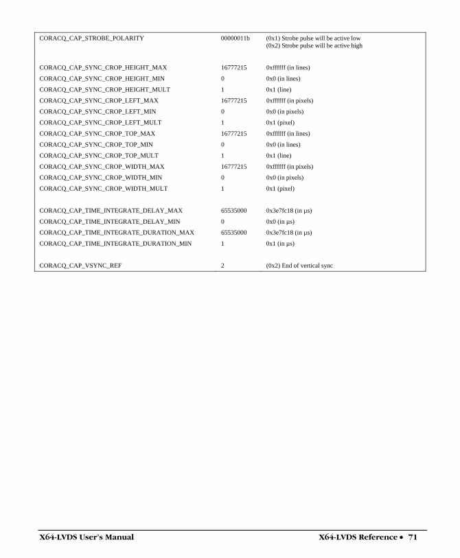
X64-LVDS User's Manual X64-LVDS Reference • 71
CORACQ_CAP_STROBE_POLARITY 00000011b (0x1) Strobe pulse will be active low (0x2) Strobe pulse will be active high
CORACQ_CAP_SYNC_CROP_HEIGHT_MAX 16777215 0xffffff (in lines)
CORACQ_CAP_SYNC_CROP_HEIGHT_MIN 0 0x0 (in lines)
CORACQ_CAP_SYNC_CROP_HEIGHT_MULT 1 0x1 (line)
CORACQ_CAP_SYNC_CROP_LEFT_MAX 16777215 0xffffff (in pixels)
CORACQ_CAP_SYNC_CROP_LEFT_MIN 0 0x0 (in pixels)
CORACQ_CAP_SYNC_CROP_LEFT_MULT 1 0x1 (pixel)
CORACQ_CAP_SYNC_CROP_TOP_MAX 16777215 0xffffff (in lines)
CORACQ_CAP_SYNC_CROP_TOP_MIN 0 0x0 (in lines)
CORACQ_CAP_SYNC_CROP_TOP_MULT 1 0x1 (line)
CORACQ_CAP_SYNC_CROP_WIDTH_MAX 16777215 0xffffff (in pixels)
CORACQ_CAP_SYNC_CROP_WIDTH_MIN 0 0x0 (in pixels)
CORACQ_CAP_SYNC_CROP_WIDTH_MULT 1 0x1 (pixel)
CORACQ_CAP_TIME_INTEGRATE_DELAY_MAX 65535000 0x3e7fc18 (in µs)
CORACQ_CAP_TIME_INTEGRATE_DELAY_MIN 0 0x0 (in µs)
CORACQ_CAP_TIME_INTEGRATE_DURATION_MAX 65535000 0x3e7fc18 (in µs)
CORACQ_CAP_TIME_INTEGRATE_DURATION_MIN 1 0x1 (in µs)
CORACQ_CAP_VSYNC_REF 2 (0x2) End of vertical sync
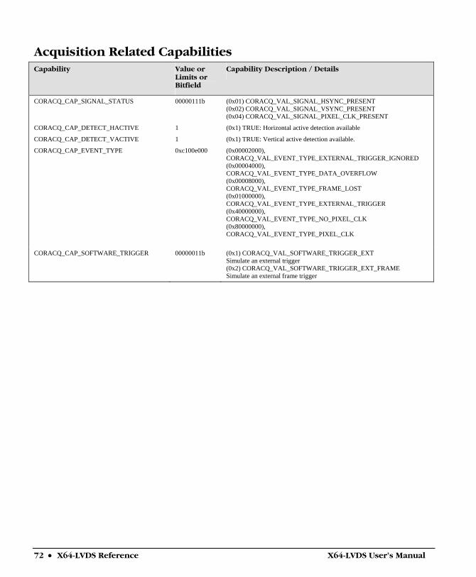
72 • X64-LVDS Reference X64-LVDS User's Manual
Acquisition Related Capabilities Capability Value or
Limits or Bitfield
Capability Description / Details
CORACQ_CAP_SIGNAL_STATUS 00000111b (0x01) CORACQ_VAL_SIGNAL_HSYNC_PRESENT (0x02) CORACQ_VAL_SIGNAL_VSYNC_PRESENT (0x04) CORACQ_VAL_SIGNAL_PIXEL_CLK_PRESENT
CORACQ_CAP_DETECT_HACTIVE 1 (0x1) TRUE: Horizontal active detection available
CORACQ_CAP_DETECT_VACTIVE 1 (0x1) TRUE: Vertical active detection available.
CORACQ_CAP_EVENT_TYPE 0xc100e000 (0x00002000), CORACQ_VAL_EVENT_TYPE_EXTERNAL_TRIGGER_IGNORED (0x00004000), CORACQ_VAL_EVENT_TYPE_DATA_OVERFLOW (0x00008000), CORACQ_VAL_EVENT_TYPE_FRAME_LOST (0x01000000), CORACQ_VAL_EVENT_TYPE_EXTERNAL_TRIGGER (0x40000000), CORACQ_VAL_EVENT_TYPE_NO_PIXEL_CLK (0x80000000), CORACQ_VAL_EVENT_TYPE_PIXEL_CLK
CORACQ_CAP_SOFTWARE_TRIGGER 00000011b (0x1) CORACQ_VAL_SOFTWARE_TRIGGER_EXT Simulate an external trigger (0x2) CORACQ_VAL_SOFTWARE_TRIGGER_EXT_FRAME Simulate an external frame trigger
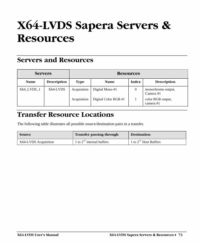
X64-LVDS User's Manual X64-LVDS Sapera Servers & Resources • 73
X64-LVDS Sapera Servers & Resources
Servers and Resources
Servers Resources
Name Description Type Name Index Description
X64_LVDS_1 X64-LVDS Acquisition Digital Mono #1 0 monochrome output, Camera #1
Acquisition Digital Color RGB #1 1 color RGB output, camera #1
Transfer Resource Locations The following table illustrates all possible source/destination pairs in a transfer.
Source Transfer passing through Destination
X64-LVDS Acquisition 1 to 217 internal buffers 1 to 217 Host Buffers

74 • X64-LVDS Sapera Servers & Resources X64-LVDS User's Manual
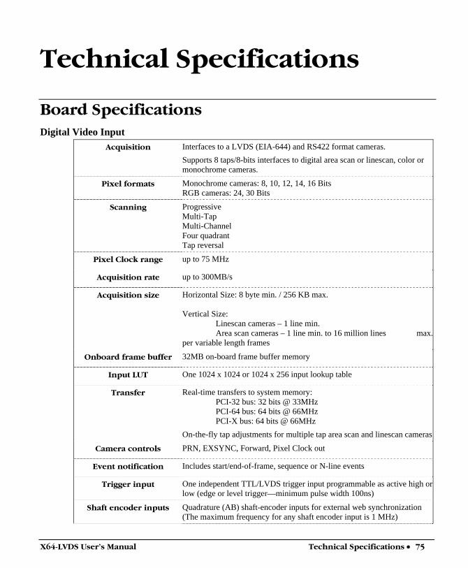
X64-LVDS User's Manual Technical Specifications • 75
Technical Specifications
Board Specifications Digital Video Input
Acquisition Interfaces to a LVDS (EIA-644) and RS422 format cameras. Supports 8 taps/8-bits interfaces to digital area scan or linescan, color or monochrome cameras.
Pixel formats Monochrome cameras: 8, 10, 12, 14, 16 Bits RGB cameras: 24, 30 Bits
Scanning Progressive Multi-Tap Multi-Channel Four quadrant Tap reversal
Pixel Clock range up to 75 MHz
Acquisition rate up to 300MB/s
Acquisition size Horizontal Size: 8 byte min. / 256 KB max. Vertical Size: Linescan cameras – 1 line min. Area scan cameras – 1 line min. to 16 million lines max. per variable length frames
Onboard frame buffer 32MB on-board frame buffer memory
Input LUT One 1024 x 1024 or 1024 x 256 input lookup table
Transfer Real-time transfers to system memory: PCI-32 bus: 32 bits @ 33MHz PCI-64 bus: 64 bits @ 66MHz PCI-X bus: 64 bits @ 66MHz On-the-fly tap adjustments for multiple tap area scan and linescan cameras
Camera controls PRN, EXSYNC, Forward, Pixel Clock out
Event notification Includes start/end-of-frame, sequence or N-line events
Trigger input One independent TTL/LVDS trigger input programmable as active high or low (edge or level trigger—minimum pulse width 100ns)
Shaft encoder inputs Quadrature (AB) shaft-encoder inputs for external web synchronization (The maximum frequency for any shaft encoder input is 1 MHz)
76 • Technical Specifications X64-LVDS User's Manual
Strobe output One strobe TTL output
Additional I/O signals Use the optional X-I/O module providing 8 input & 8 output general I/Os
Serial Port Supports communication speeds 9600 to 115 kbps
Development software Supported by Sapera LT and Sapera Processing programming libraries. Application development using C/C++ DLLs and ActiveX controls with Microsoft Visual Studio® or Visual Basic version 6.0.
X64-LVDS Physical Dimensions
Approximately 6.7 in. (17 cm) wide by 4.2 in. (10.7 cm) high (conforms to half length PCI)
Host System Requirements General System Requirements for the X64-LVDS Series
Computer system with a 64 bit – 66/33 MHz PCI slot or a 32 bit – 33 MHz PCI slot. Compatible with 5V or 3.3 V slots.
Operating System Support
Windows NT 4.0 SP6 and Windows 2000 SP1 and Windows XP
Power Requirements +5 Volt 2 amp typical Note: other internal voltages are derived from +5V +12 Volt As per camera connected and supplied by X64-LVDS PC power interface
Environment Ambient Temperature: 10° to 50° C (operation)
0° to 70° C (storage) Relative Humidity: 5% to 90% non-condensing (operating)
0% to 95% (storage)
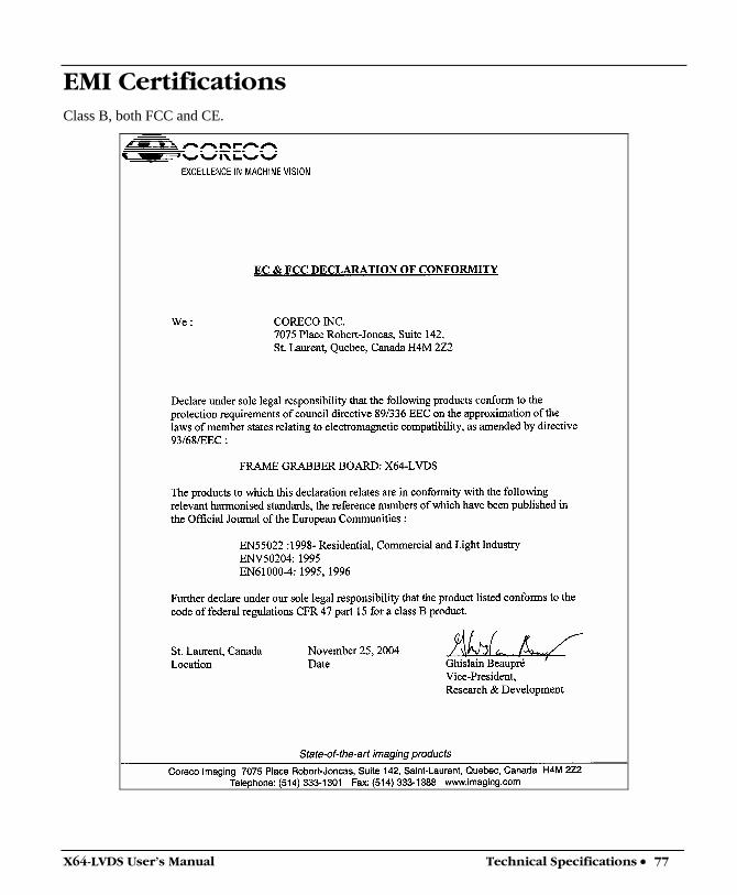
X64-LVDS User's Manual Technical Specifications • 77
EMI Certifications Class B, both FCC and CE.
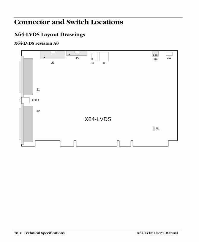
78 • Technical Specifications X64-LVDS User's Manual
Connector and Switch Locations
X64-LVDS Layout Drawings
X64-LVDS revision A0
J2
LED 1
J8 J9J10 J12
J1
J11
X64-LVDS
J5J3
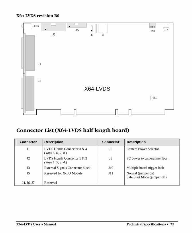
X64-LVDS User's Manual Technical Specifications • 79
X64-LVDS revision B0
J2
LEDs
J8 J9J10 J12
J1
J11
X64-LVDS
J5J3
Connector List (X64-LVDS half length board)
Connector Description Connector Description
J1 LVDS Honda Connector 3 & 4 ( taps 5, 6, 7, 8 )
J8 Camera Power Selector
J2 LVDS Honda Connector 1 & 2 ( taps 1, 2, 3, 4 )
J9 PC power to camera interface.
J3 External Signals Connector block J10 Multiple board trigger lock J5 Reserved for X-I/O Module J11 Normal (jumper on)
Safe Start Mode (jumper off) J4, J6, J7 Reserved
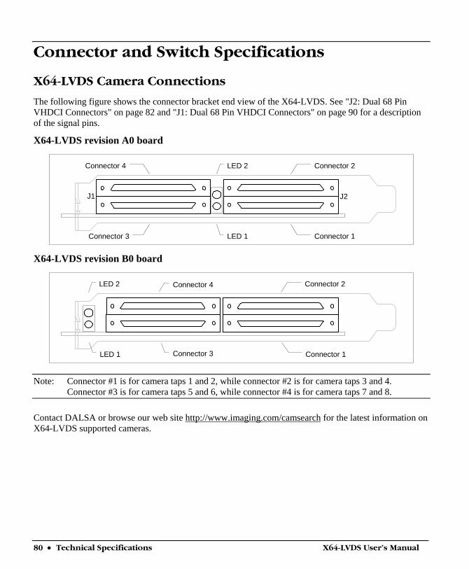
80 • Technical Specifications X64-LVDS User's Manual
Connector and Switch Specifications
X64-LVDS Camera Connections
The following figure shows the connector bracket end view of the X64-LVDS. See "J2: Dual 68 Pin VHDCI Connectors" on page 82 and "J1: Dual 68 Pin VHDCI Connectors" on page 90 for a description of the signal pins.
X64-LVDS revision A0 board
Connector 4
Connector 3 Connector 1
Connector 2
LED 1
LED 2
J1 J2
X64-LVDS revision B0 board
Connector 4
Connector 3 Connector 1
Connector 2
LED 1
LED 2
Note: Connector #1 is for camera taps 1 and 2, while connector #2 is for camera taps 3 and 4. Connector #3 is for camera taps 5 and 6, while connector #4 is for camera taps 7 and 8.
Contact DALSA or browse our web site http://www.imaging.com/camsearch for the latest information on X64-LVDS supported cameras.
X64-LVDS User's Manual Technical Specifications • 81
Status LED Functional Description • Red: No camera connected or camera has no power. • Green: Camera connected and is ON. Camera clock detected. No line valid detected. • Slow Flashing Green: Camera Line Valid signal detected. • Fast Flashing Green: Image grab in progress.
Programmable Camera Controls
Both J1 and J2 have four programmable camera control signals (LVDS pairs). These controls (CC1, CC2, CC3, CC4) are configured with CamExpert and saved into the camera control file for the camera used. The following table lists the available signals and the default assignment for each camera control. Refer to the connector pinout descriptions that follow in this manual.
Control Signal Description Default Assignment
EXSYNC CC1 default PRIN CC2 default
Forward CC3 default Pixel Clock out CC4 default
Logic Hi Logic Low
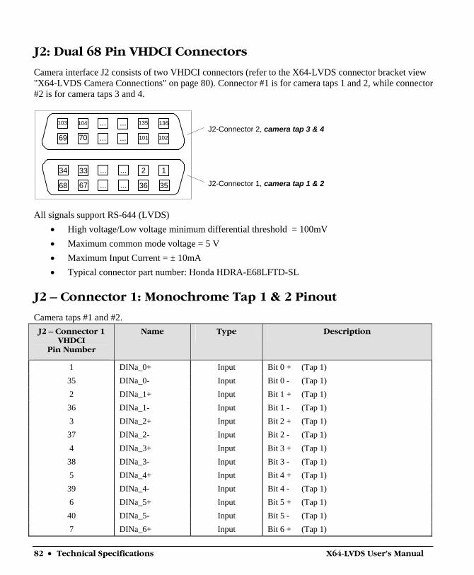
82 • Technical Specifications X64-LVDS User's Manual
J2: Dual 68 Pin VHDCI Connectors
Camera interface J2 consists of two VHDCI connectors (refer to the X64-LVDS connector bracket view "X64-LVDS Camera Connections" on page 80). Connector #1 is for camera taps 1 and 2, while connector #2 is for camera taps 3 and 4.
33
67
...
...
34 2
68 36 35
1...
...
70 ...
...
69 101
103
102...
...104 135 136J2-Connector 2, camera tap 3 & 4
J2-Connector 1, camera tap 1 & 2
All signals support RS-644 (LVDS)
• High voltage/Low voltage minimum differential threshold = 100mV • Maximum common mode voltage = 5 V • Maximum Input Current = ± 10mA • Typical connector part number: Honda HDRA-E68LFTD-SL
J2 – Connector 1: Monochrome Tap 1 & 2 Pinout
Camera taps #1 and #2. J2 – Connector 1
VHDCI Pin Number
Name Type Description
1 DINa_0+ Input Bit 0 + (Tap 1) 35 DINa_0- Input Bit 0 - (Tap 1) 2 DINa_1+ Input Bit 1 + (Tap 1)
36 DINa_1- Input Bit 1 - (Tap 1) 3 DINa_2+ Input Bit 2 + (Tap 1)
37 DINa_2- Input Bit 2 - (Tap 1) 4 DINa_3+ Input Bit 3 + (Tap 1)
38 DINa_3- Input Bit 3 - (Tap 1) 5 DINa_4+ Input Bit 4 + (Tap 1)
39 DINa_4- Input Bit 4 - (Tap 1) 6 DINa_5+ Input Bit 5 + (Tap 1)
40 DINa_5- Input Bit 5 - (Tap 1) 7 DINa_6+ Input Bit 6 + (Tap 1)
X64-LVDS User's Manual Technical Specifications • 83
41 DINa_6- Input Bit 6 - (Tap 1) 8 DINa_7+ Input Bit 7 + (Tap 1)
42 DINa_7- Input Bit 7 - (Tap 1) 9, 43 GND Ground 10 DINb_0+ Input Bit 0 + (Tap 2) 44 DINb_0- Input Bit 0 - (Tap 2) 11 DINb_1+ Input Bit 1 + (Tap 2) 45 DINb_1- Input Bit 1 - (Tap 2) 12 DINb_2+ Input Bit 2 + (Tap 2) 46 DINb_2- Input Bit 2 - (Tap 2) 13 DINb_3+ Input Bit 3 + (Tap 2) 47 DINb_3- Input Bit 3 - (Tap 2) 14 DINb_4+ Input Bit 4 + (Tap 2) 48 DINb_4- Input Bit 4 - (Tap 2) 15 DINb_5+ Input Bit 5 + (Tap 2) 49 DINb_5- Input Bit 5 - (Tap 2) 16 DINb_6+ Input Bit 6 + (Tap 2) 50 DINb_6- Input Bit 6 - (Tap 2) 17 DINb_7+ Input Bit 7 + (Tap 2) 51 DINb_7- Input Bit 7 - (Tap 2)
18, 52 GND Ground 19 PHA+ Input Shaft Encoder Phase A + 53 PHA- Input Shaft Encoder Phase A - 20 PHB+ Input Shaft Encoder Phase B + 54 PHB- Input Shaft Encoder Phase B - 21 Trig1+ Input External Trigger 1 + 55 Trig1- Input External Trigger 1 - 22 Out12V Output 12 Volt Source (fused – power off reset) 56 Out12V Output 12 Volt Source (fused – power off reset) 23 cam CC2+ Output
(default: PRIN) Programmable Camera Control 2 + (see Programmable Camera Controls)
57 cam CC2- Output Programmable Camera Control 2 - 24 cam CC1+ Output
(default: EXSYNC) Programmable Camera Control 1 +
58 cam CC1- Output Programmable Camera Control 1 - 25 cam CC3+ Output
(default: Forward) Programmable Camera Control 3 +
59 cam CC3- Output Programmable Camera Control 3 -
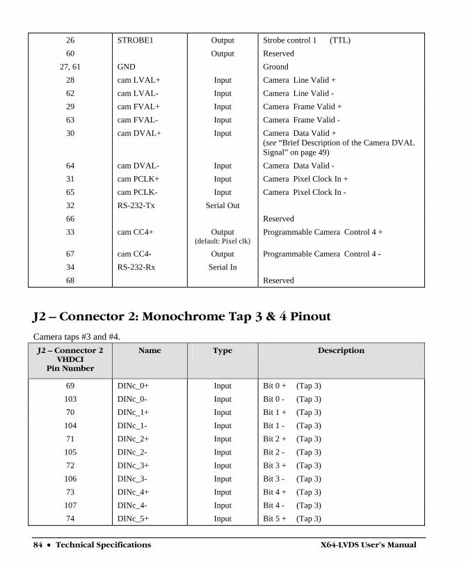
84 • Technical Specifications X64-LVDS User's Manual
26 STROBE1 Output Strobe control 1 (TTL) 60 Output Reserved
27, 61 GND Ground 28 cam LVAL+ Input Camera Line Valid + 62 cam LVAL- Input Camera Line Valid - 29 cam FVAL+ Input Camera Frame Valid + 63 cam FVAL- Input Camera Frame Valid - 30 cam DVAL+ Input Camera Data Valid +
(see “Brief Description of the Camera DVAL Signal” on page 49)
64 cam DVAL- Input Camera Data Valid - 31 cam PCLK+ Input Camera Pixel Clock In + 65 cam PCLK- Input Camera Pixel Clock In - 32 RS-232-Tx Serial Out 66 Reserved 33 cam CC4+ Output
(default: Pixel clk) Programmable Camera Control 4 +
67 cam CC4- Output Programmable Camera Control 4 - 34 RS-232-Rx Serial In 68 Reserved
J2 – Connector 2: Monochrome Tap 3 & 4 Pinout
Camera taps #3 and #4. J2 – Connector 2
VHDCI Pin Number
Name Type Description
69 DINc_0+ Input Bit 0 + (Tap 3) 103 DINc_0- Input Bit 0 - (Tap 3) 70 DINc_1+ Input Bit 1 + (Tap 3) 104 DINc_1- Input Bit 1 - (Tap 3) 71 DINc_2+ Input Bit 2 + (Tap 3) 105 DINc_2- Input Bit 2 - (Tap 3) 72 DINc_3+ Input Bit 3 + (Tap 3) 106 DINc_3- Input Bit 3 - (Tap 3) 73 DINc_4+ Input Bit 4 + (Tap 3) 107 DINc_4- Input Bit 4 - (Tap 3) 74 DINc_5+ Input Bit 5 + (Tap 3)
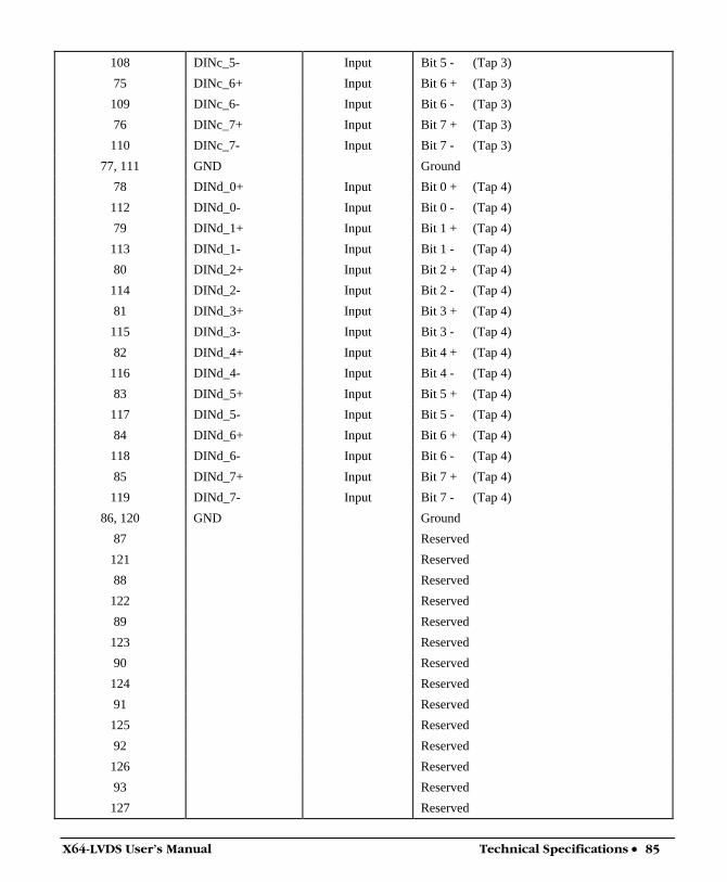
X64-LVDS User's Manual Technical Specifications • 85
108 DINc_5- Input Bit 5 - (Tap 3) 75 DINc_6+ Input Bit 6 + (Tap 3) 109 DINc_6- Input Bit 6 - (Tap 3) 76 DINc_7+ Input Bit 7 + (Tap 3) 110 DINc_7- Input Bit 7 - (Tap 3)
77, 111 GND Ground 78 DINd_0+ Input Bit 0 + (Tap 4) 112 DINd_0- Input Bit 0 - (Tap 4) 79 DINd_1+ Input Bit 1 + (Tap 4) 113 DINd_1- Input Bit 1 - (Tap 4) 80 DINd_2+ Input Bit 2 + (Tap 4) 114 DINd_2- Input Bit 2 - (Tap 4) 81 DINd_3+ Input Bit 3 + (Tap 4) 115 DINd_3- Input Bit 3 - (Tap 4) 82 DINd_4+ Input Bit 4 + (Tap 4) 116 DINd_4- Input Bit 4 - (Tap 4) 83 DINd_5+ Input Bit 5 + (Tap 4) 117 DINd_5- Input Bit 5 - (Tap 4) 84 DINd_6+ Input Bit 6 + (Tap 4) 118 DINd_6- Input Bit 6 - (Tap 4) 85 DINd_7+ Input Bit 7 + (Tap 4) 119 DINd_7- Input Bit 7 - (Tap 4)
86, 120 GND Ground 87 Reserved 121 Reserved 88 Reserved 122 Reserved 89 Reserved 123 Reserved 90 Reserved 124 Reserved 91 Reserved 125 Reserved 92 Reserved 126 Reserved 93 Reserved 127 Reserved
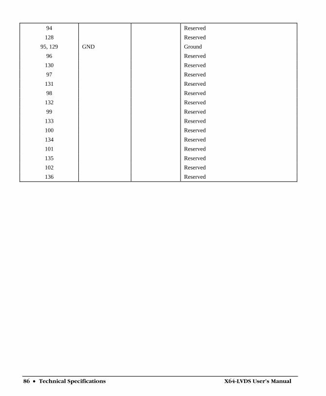
86 • Technical Specifications X64-LVDS User's Manual
94 Reserved 128 Reserved
95, 129 GND Ground 96 Reserved 130 Reserved 97 Reserved 131 Reserved 98 Reserved 132 Reserved 99 Reserved 133 Reserved 100 Reserved 134 Reserved 101 Reserved 135 Reserved 102 Reserved 136 Reserved
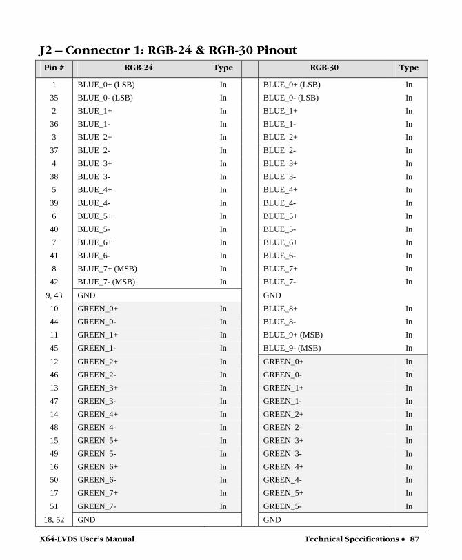
X64-LVDS User's Manual Technical Specifications • 87
J2 – Connector 1: RGB-24 & RGB-30 Pinout Pin # RGB-24 Type RGB-30 Type
1 BLUE_0+ (LSB) In BLUE_0+ (LSB) In 35 BLUE_0- (LSB) In BLUE_0- (LSB) In 2 BLUE_1+ In BLUE_1+ In
36 BLUE_1- In BLUE_1- In 3 BLUE_2+ In BLUE_2+ In
37 BLUE_2- In BLUE_2- In 4 BLUE_3+ In BLUE_3+ In
38 BLUE_3- In BLUE_3- In 5 BLUE_4+ In BLUE_4+ In
39 BLUE_4- In BLUE_4- In 6 BLUE_5+ In BLUE_5+ In
40 BLUE_5- In BLUE_5- In 7 BLUE_6+ In BLUE_6+ In
41 BLUE_6- In BLUE_6- In 8 BLUE_7+ (MSB) In BLUE_7+ In
42 BLUE_7- (MSB) In BLUE_7- In
9, 43 GND GND 10 GREEN_0+ In BLUE_8+ In 44 GREEN_0- In BLUE_8- In 11 GREEN_1+ In BLUE_9+ (MSB) In 45 GREEN_1- In BLUE_9- (MSB) In
12 GREEN_2+ In GREEN_0+ In 46 GREEN_2- In GREEN_0- In 13 GREEN_3+ In GREEN_1+ In 47 GREEN_3- In GREEN_1- In 14 GREEN_4+ In GREEN_2+ In 48 GREEN_4- In GREEN_2- In 15 GREEN_5+ In GREEN_3+ In 49 GREEN_5- In GREEN_3- In 16 GREEN_6+ In GREEN_4+ In 50 GREEN_6- In GREEN_4- In 17 GREEN_7+ In GREEN_5+ In 51 GREEN_7- In GREEN_5- In
18, 52 GND GND
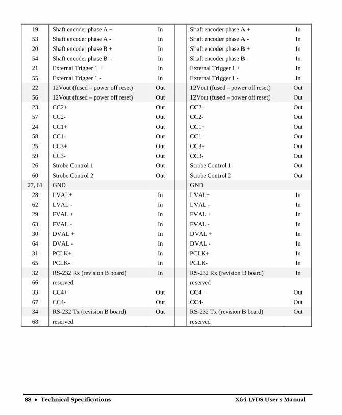
88 • Technical Specifications X64-LVDS User's Manual
19 Shaft encoder phase A + In Shaft encoder phase A + In 53 Shaft encoder phase A - In Shaft encoder phase A - In 20 Shaft encoder phase B + In Shaft encoder phase B + In 54 Shaft encoder phase B - In Shaft encoder phase B - In 21 External Trigger 1 + In External Trigger 1 + In 55 External Trigger 1 - In External Trigger 1 - In 22 12Vout (fused – power off reset) Out 12Vout (fused – power off reset) Out 56 12Vout (fused – power off reset) Out 12Vout (fused – power off reset) Out 23 CC2+ Out CC2+ Out 57 CC2- Out CC2- Out 24 CC1+ Out CC1+ Out 58 CC1- Out CC1- Out 25 CC3+ Out CC3+ Out 59 CC3- Out CC3- Out 26 Strobe Control 1 Out Strobe Control 1 Out 60 Strobe Control 2 Out Strobe Control 2 Out
27, 61 GND GND 28 LVAL+ In LVAL+ In 62 LVAL - In LVAL - In 29 FVAL + In FVAL + In 63 FVAL - In FVAL - In 30 DVAL + In DVAL + In 64 DVAL - In DVAL - In 31 PCLK+ In PCLK+ In 65 PCLK- In PCLK- In 32 RS-232 Rx (revision B board) In RS-232 Rx (revision B board) In 66 reserved reserved 33 CC4+ Out CC4+ Out 67 CC4- Out CC4- Out 34 RS-232 Tx (revision B board) Out RS-232 Tx (revision B board) Out 68 reserved reserved
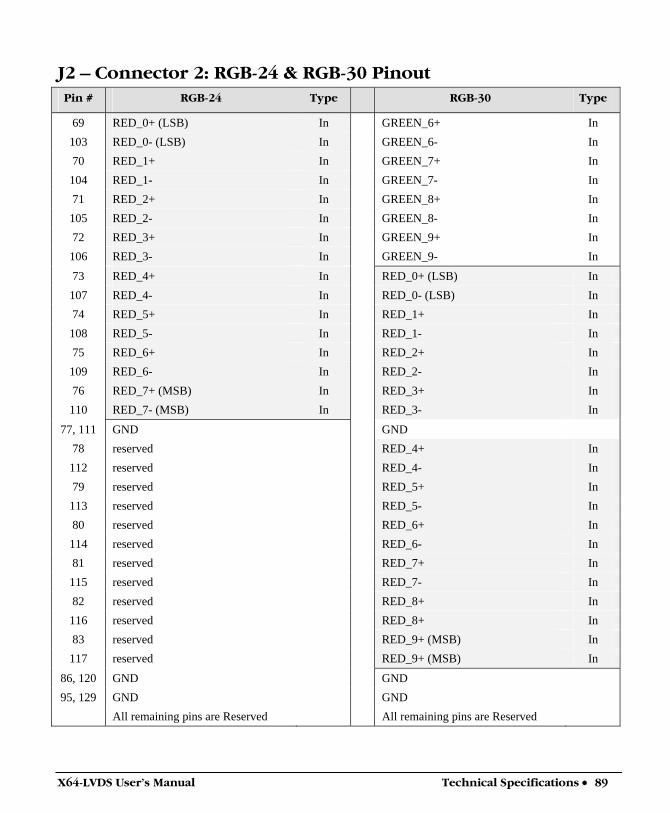
X64-LVDS User's Manual Technical Specifications • 89
J2 – Connector 2: RGB-24 & RGB-30 Pinout Pin # RGB-24 Type RGB-30 Type
69 RED_0+ (LSB) In GREEN_6+ In 103 RED_0- (LSB) In GREEN_6- In 70 RED_1+ In GREEN_7+ In 104 RED_1- In GREEN_7- In 71 RED_2+ In GREEN_8+ In 105 RED_2- In GREEN_8- In 72 RED_3+ In GREEN_9+ In 106 RED_3- In GREEN_9- In
73 RED_4+ In RED_0+ (LSB) In 107 RED_4- In RED_0- (LSB) In 74 RED_5+ In RED_1+ In 108 RED_5- In RED_1- In 75 RED_6+ In RED_2+ In 109 RED_6- In RED_2- In 76 RED_7+ (MSB) In RED_3+ In 110 RED_7- (MSB) In RED_3- In
77, 111 GND GND 78 reserved RED_4+ In 112 reserved RED_4- In 79 reserved RED_5+ In 113 reserved RED_5- In 80 reserved RED_6+ In 114 reserved RED_6- In 81 reserved RED_7+ In 115 reserved RED_7- In 82 reserved RED_8+ In 116 reserved RED_8+ In 83 reserved RED_9+ (MSB) In 117 reserved RED_9+ (MSB) In
86, 120 GND GND 95, 129 GND GND
All remaining pins are Reserved All remaining pins are Reserved
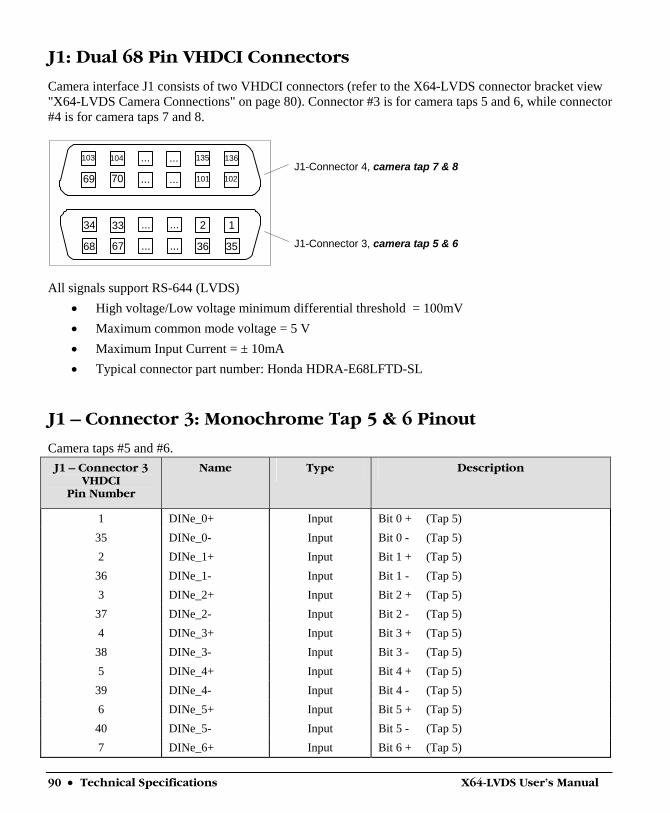
90 • Technical Specifications X64-LVDS User's Manual
J1: Dual 68 Pin VHDCI Connectors
Camera interface J1 consists of two VHDCI connectors (refer to the X64-LVDS connector bracket view "X64-LVDS Camera Connections" on page 80). Connector #3 is for camera taps 5 and 6, while connector #4 is for camera taps 7 and 8.
33
67
...
...
34 2
68 36 35
1...
...
70 ...
...
69 101
103
102...
...104 135 136J1-Connector 4, camera tap 7 & 8
J1-Connector 3, camera tap 5 & 6
All signals support RS-644 (LVDS)
• High voltage/Low voltage minimum differential threshold = 100mV • Maximum common mode voltage = 5 V • Maximum Input Current = ± 10mA • Typical connector part number: Honda HDRA-E68LFTD-SL
J1 – Connector 3: Monochrome Tap 5 & 6 Pinout
Camera taps #5 and #6. J1 – Connector 3
VHDCI Pin Number
Name Type Description
1 DINe_0+ Input Bit 0 + (Tap 5) 35 DINe_0- Input Bit 0 - (Tap 5) 2 DINe_1+ Input Bit 1 + (Tap 5)
36 DINe_1- Input Bit 1 - (Tap 5) 3 DINe_2+ Input Bit 2 + (Tap 5)
37 DINe_2- Input Bit 2 - (Tap 5) 4 DINe_3+ Input Bit 3 + (Tap 5)
38 DINe_3- Input Bit 3 - (Tap 5) 5 DINe_4+ Input Bit 4 + (Tap 5)
39 DINe_4- Input Bit 4 - (Tap 5) 6 DINe_5+ Input Bit 5 + (Tap 5)
40 DINe_5- Input Bit 5 - (Tap 5) 7 DINe_6+ Input Bit 6 + (Tap 5)
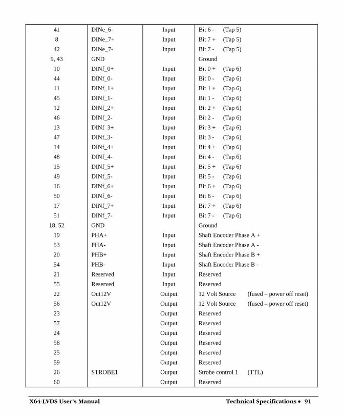
X64-LVDS User's Manual Technical Specifications • 91
41 DINe_6- Input Bit 6 - (Tap 5) 8 DINe_7+ Input Bit 7 + (Tap 5)
42 DINe_7- Input Bit 7 - (Tap 5) 9, 43 GND Ground 10 DINf_0+ Input Bit 0 + (Tap 6) 44 DINf_0- Input Bit 0 - (Tap 6) 11 DINf_1+ Input Bit 1 + (Tap 6) 45 DINf_1- Input Bit 1 - (Tap 6) 12 DINf_2+ Input Bit 2 + (Tap 6) 46 DINf_2- Input Bit 2 - (Tap 6) 13 DINf_3+ Input Bit 3 + (Tap 6) 47 DINf_3- Input Bit 3 - (Tap 6) 14 DINf_4+ Input Bit 4 + (Tap 6) 48 DINf_4- Input Bit 4 - (Tap 6) 15 DINf_5+ Input Bit 5 + (Tap 6) 49 DINf_5- Input Bit 5 - (Tap 6) 16 DINf_6+ Input Bit 6 + (Tap 6) 50 DINf_6- Input Bit 6 - (Tap 6) 17 DINf_7+ Input Bit 7 + (Tap 6) 51 DINf_7- Input Bit 7 - (Tap 6)
18, 52 GND Ground 19 PHA+ Input Shaft Encoder Phase A + 53 PHA- Input Shaft Encoder Phase A - 20 PHB+ Input Shaft Encoder Phase B + 54 PHB- Input Shaft Encoder Phase B - 21 Reserved Input Reserved 55 Reserved Input Reserved 22 Out12V Output 12 Volt Source (fused – power off reset) 56 Out12V Output 12 Volt Source (fused – power off reset) 23 Output Reserved 57 Output Reserved 24 Output Reserved 58 Output Reserved 25 Output Reserved 59 Output Reserved 26 STROBE1 Output Strobe control 1 (TTL) 60 Output Reserved
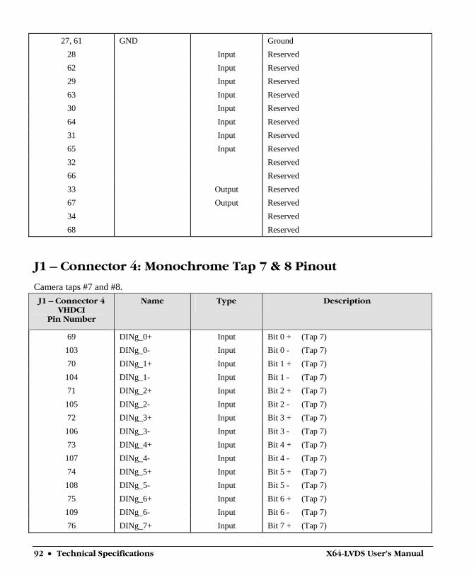
92 • Technical Specifications X64-LVDS User's Manual
27, 61 GND Ground 28 Input Reserved 62 Input Reserved 29 Input Reserved 63 Input Reserved 30 Input Reserved 64 Input Reserved 31 Input Reserved 65 Input Reserved 32 Reserved 66 Reserved 33 Output Reserved 67 Output Reserved 34 Reserved 68 Reserved
J1 – Connector 4: Monochrome Tap 7 & 8 Pinout
Camera taps #7 and #8. J1 – Connector 4
VHDCI Pin Number
Name Type Description
69 DINg_0+ Input Bit 0 + (Tap 7) 103 DINg_0- Input Bit 0 - (Tap 7) 70 DINg_1+ Input Bit 1 + (Tap 7) 104 DINg_1- Input Bit 1 - (Tap 7) 71 DINg_2+ Input Bit 2 + (Tap 7) 105 DINg_2- Input Bit 2 - (Tap 7) 72 DINg_3+ Input Bit 3 + (Tap 7) 106 DINg_3- Input Bit 3 - (Tap 7) 73 DINg_4+ Input Bit 4 + (Tap 7) 107 DINg_4- Input Bit 4 - (Tap 7) 74 DINg_5+ Input Bit 5 + (Tap 7) 108 DINg_5- Input Bit 5 - (Tap 7) 75 DINg_6+ Input Bit 6 + (Tap 7) 109 DINg_6- Input Bit 6 - (Tap 7) 76 DINg_7+ Input Bit 7 + (Tap 7)
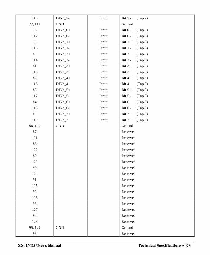
X64-LVDS User's Manual Technical Specifications • 93
110 DINg_7- Input Bit 7 - (Tap 7) 77, 111 GND Ground
78 DINh_0+ Input Bit 0 + (Tap 8) 112 DINh_0- Input Bit 0 - (Tap 8) 79 DINh_1+ Input Bit 1 + (Tap 8) 113 DINh_1- Input Bit 1 - (Tap 8) 80 DINh_2+ Input Bit 2 + (Tap 8) 114 DINh_2- Input Bit 2 - (Tap 8) 81 DINh_3+ Input Bit 3 + (Tap 8) 115 DINh_3- Input Bit 3 - (Tap 8) 82 DINh_4+ Input Bit 4 + (Tap 8) 116 DINh_4- Input Bit 4 - (Tap 8) 83 DINh_5+ Input Bit 5 + (Tap 8) 117 DINh_5- Input Bit 5 - (Tap 8) 84 DINh_6+ Input Bit 6 + (Tap 8) 118 DINh_6- Input Bit 6 - (Tap 8) 85 DINh_7+ Input Bit 7 + (Tap 8) 119 DINh_7- Input Bit 7 - (Tap 8)
86, 120 GND Ground 87 Reserved 121 Reserved 88 Reserved 122 Reserved 89 Reserved 123 Reserved 90 Reserved 124 Reserved 91 Reserved 125 Reserved 92 Reserved 126 Reserved 93 Reserved 127 Reserved 94 Reserved 128 Reserved
95, 129 GND Ground 96 Reserved
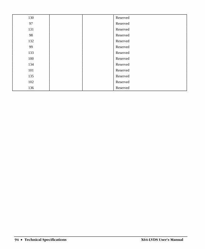
94 • Technical Specifications X64-LVDS User's Manual
130 Reserved 97 Reserved 131 Reserved 98 Reserved 132 Reserved 99 Reserved 133 Reserved 100 Reserved 134 Reserved 101 Reserved 135 Reserved 102 Reserved 136 Reserved
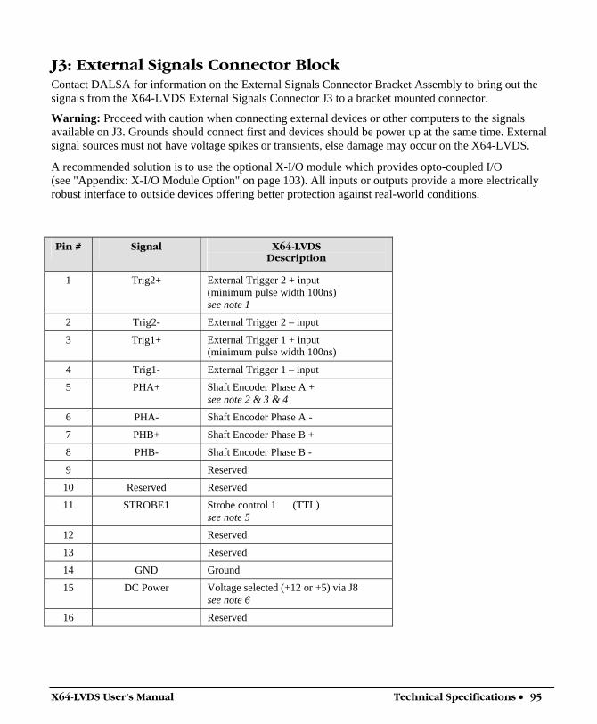
X64-LVDS User's Manual Technical Specifications • 95
J3: External Signals Connector Block Contact DALSA for information on the External Signals Connector Bracket Assembly to bring out the signals from the X64-LVDS External Signals Connector J3 to a bracket mounted connector.
Warning: Proceed with caution when connecting external devices or other computers to the signals available on J3. Grounds should connect first and devices should be power up at the same time. External signal sources must not have voltage spikes or transients, else damage may occur on the X64-LVDS.
A recommended solution is to use the optional X-I/O module which provides opto-coupled I/O (see "Appendix: X-I/O Module Option" on page 103). All inputs or outputs provide a more electrically robust interface to outside devices offering better protection against real-world conditions.
Pin # Signal X64-LVDS
Description
1 Trig2+ External Trigger 2 + input (minimum pulse width 100ns) see note 1
2 Trig2- External Trigger 2 – input
3 Trig1+ External Trigger 1 + input (minimum pulse width 100ns)
4 Trig1- External Trigger 1 – input
5 PHA+ Shaft Encoder Phase A + see note 2 & 3 & 4
6 PHA- Shaft Encoder Phase A -
7 PHB+ Shaft Encoder Phase B +
8 PHB- Shaft Encoder Phase B -
9 Reserved
10 Reserved Reserved
11 STROBE1 Strobe control 1 (TTL) see note 5
12 Reserved
13 Reserved
14 GND Ground
15 DC Power Voltage selected (+12 or +5) via J8 see note 6
16 Reserved
96 • Technical Specifications X64-LVDS User's Manual
Notes for X64-LVDS External Signals Connector 1. Refer to Sapera parameters
CORACQ_PRM_EXT_TRIGGER_LEVEL CORACQ_PRM_EXT_FRAME_TRIGGER_LEVEL CORACQ_PRM_EXT_TRIGGER_ENABLE CORACQ_PRM_EXT_TRIGGER_DETECTION
2. See "Line Trigger Source Selection for Linescan Applications" on page 50 for more information. Refer to Sapera parameters CORACQ_PRM_SHAFT_ENCODER_ENABLE CORACQ_PRM_SHAFT_ENCODER_DROP or refer to CORACQ_PRM_EXT_LINE_TRIGGER_ENABLE CORACQ_PRM_EXT_LINE_TRIGGER_DETECTION CORACQ_PRM_EXT_LINE_TRIGGER_LEVEL (fixed at LVDS) CORACQ_PRM_EXT_LINE_TRIGGER_SOURCE
3. Important: When using only one shaft encoder input phase, say phase A, then the phase B inputs must be terminated by connecting phase B- to board ground available on any pin labeled GND and phase B+ to any DC source with a minimum of 100 mV positive relative to the phase B- input.
4. See "Connecting a TTL Shaft Encoder Signal to the LVDS/RS422 Input" on page 98 for details on using a TTL shaft encoder signal.
5. Refer to Sapera parameters CORACQ_PRM_STROBE_ENABLE CORACQ_PRM_STROBE_POLARITY, CORACQ_PRM_STROBE_LEVEL, CORACQ_PRM_STROBE_METHOD, CORACQ_PRM_STROBE_DELAY CORACQ_PRM_STROBE_DURATION
6. The supplied host PC voltage is selected (+12 or +5) via the shorting jumper J8. A 1.5A resettable fuse is included on the board. If the fuse is tripped, power off the host computer to reset the fuse.
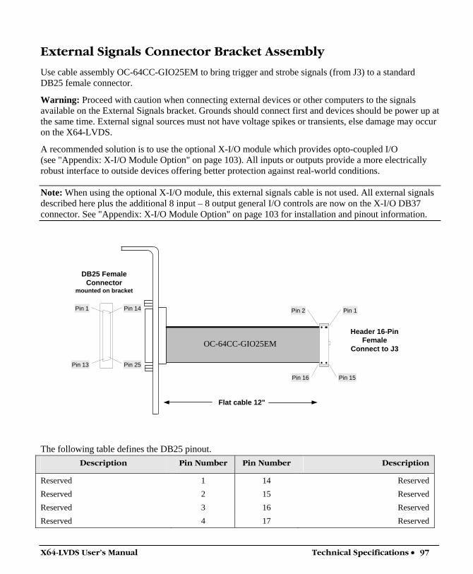
X64-LVDS User's Manual Technical Specifications • 97
External Signals Connector Bracket Assembly
Use cable assembly OC-64CC-GIO25EM to bring trigger and strobe signals (from J3) to a standard DB25 female connector.
Warning: Proceed with caution when connecting external devices or other computers to the signals available on the External Signals bracket. Grounds should connect first and devices should be power up at the same time. External signal sources must not have voltage spikes or transients, else damage may occur on the X64-LVDS.
A recommended solution is to use the optional X-I/O module which provides opto-coupled I/O (see "Appendix: X-I/O Module Option" on page 103). All inputs or outputs provide a more electrically robust interface to outside devices offering better protection against real-world conditions.
Note: When using the optional X-I/O module, this external signals cable is not used. All external signals described here plus the additional 8 input – 8 output general I/O controls are now on the X-I/O DB37 connector. See "Appendix: X-I/O Module Option" on page 103 for installation and pinout information.
DB25 FemaleConnector
mounted on bracket
Header 16-PinFemale
Connect to J3
Flat cable 12"
Pin 2
OC-64CC-GIO25EM
Pin 1
Pin 16 Pin 15
Pin 1 Pin 14
Pin 13 Pin 25
The following table defines the DB25 pinout. Description Pin Number Pin Number Description
Reserved 1 14 Reserved Reserved 2 15 Reserved Reserved 3 16 Reserved Reserved 4 17 Reserved
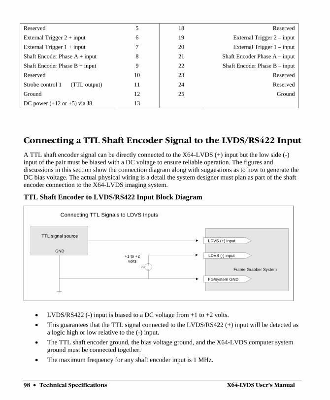
98 • Technical Specifications X64-LVDS User's Manual
Reserved 5 18 Reserved External Trigger 2 + input 6 19 External Trigger 2 – input External Trigger 1 + input 7 20 External Trigger 1 – input Shaft Encoder Phase A + input 8 21 Shaft Encoder Phase A – input Shaft Encoder Phase B + input 9 22 Shaft Encoder Phase B – input Reserved 10 23 Reserved Strobe control 1 (TTL output) 11 24 Reserved Ground 12 25 Ground DC power (+12 or +5) via J8 13
Connecting a TTL Shaft Encoder Signal to the LVDS/RS422 Input
A TTL shaft encoder signal can be directly connected to the X64-LVDS (+) input but the low side (-) input of the pair must be biased with a DC voltage to ensure reliable operation. The figures and discussions in this section show the connection diagram along with suggestions as to how to generate the DC bias voltage. The actual physical wiring is a detail the system designer must plan as part of the shaft encoder connection to the X64-LVDS imaging system.
TTL Shaft Encoder to LVDS/RS422 Input Block Diagram
LDVS (+) input
LDVS (-) input
FG/system GND
DC
+1 to +2volts
TTL signal source
GND
Frame Grabber System
Connecting TTL Signals to LDVS Inputs
• LVDS/RS422 (-) input is biased to a DC voltage from +1 to +2 volts. • This guarantees that the TTL signal connected to the LVDS/RS422 (+) input will be detected as
a logic high or low relative to the (-) input. • The TTL shaft encoder ground, the bias voltage ground, and the X64-LVDS computer system
ground must be connected together. • The maximum frequency for any shaft encoder input is 1 MHz.
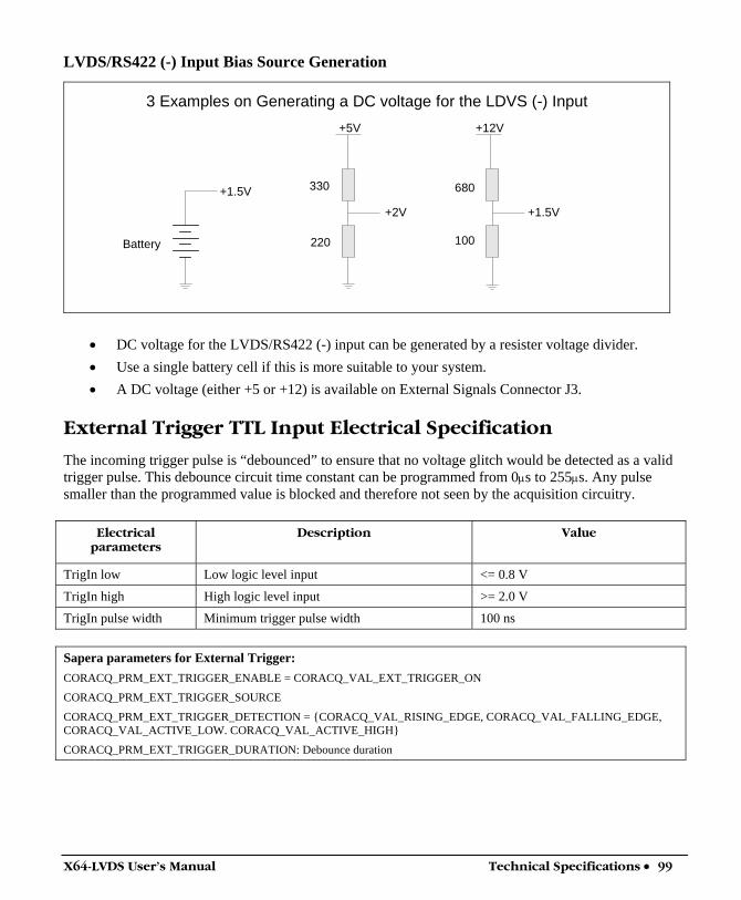
X64-LVDS User's Manual Technical Specifications • 99
LVDS/RS422 (-) Input Bias Source Generation
330
220
+5V
+2V
680
100
+12V
+1.5V
+1.5V
Battery
3 Examples on Generating a DC voltage for the LDVS (-) Input
• DC voltage for the LVDS/RS422 (-) input can be generated by a resister voltage divider. • Use a single battery cell if this is more suitable to your system. • A DC voltage (either +5 or +12) is available on External Signals Connector J3.
External Trigger TTL Input Electrical Specification
The incoming trigger pulse is “debounced” to ensure that no voltage glitch would be detected as a valid trigger pulse. This debounce circuit time constant can be programmed from 0μs to 255μs. Any pulse smaller than the programmed value is blocked and therefore not seen by the acquisition circuitry.
Electrical parameters
Description Value
TrigIn low Low logic level input <= 0.8 V
TrigIn high High logic level input >= 2.0 V
TrigIn pulse width Minimum trigger pulse width 100 ns Sapera parameters for External Trigger: CORACQ_PRM_EXT_TRIGGER_ENABLE = CORACQ_VAL_EXT_TRIGGER_ON
CORACQ_PRM_EXT_TRIGGER_SOURCE
CORACQ_PRM_EXT_TRIGGER_DETECTION = {CORACQ_VAL_RISING_EDGE, CORACQ_VAL_FALLING_EDGE, CORACQ_VAL_ACTIVE_LOW. CORACQ_VAL_ACTIVE_HIGH}
CORACQ_PRM_EXT_TRIGGER_DURATION: Debounce duration
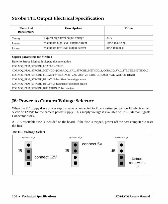
100 • Technical Specifications X64-LVDS User's Manual
Strobe TTL Output Electrical Specification
Electrical parameters
Description Value
VOH typ Typical high-level output voltage 3.9V
IOH max Maximum high-level output current -8mA (sourcing)
IOL max Maximum low-level output current 8mA (sinking) Sapera parameters for Strobe : Refer to Strobe Method in Sapera documentation CORACQ_PRM_STROBE_ENABLE = TRUE
CORACQ_PRM_STROBE_METHOD={CORACQ_VAL_STROBE_METHOD_1, CORACQ_VAL_STROBE_METHOD_2}
CORACQ_PRM_STROBE_POLARITY={CORACQ_VAL_ACTIVE_LOW, CORACQ_VAL_ACTIVE_HIGH}
CORACQ_PRM_STROBE_DELAY: Pulse offset from trigger event
CORACQ_PRM_STROBE_DELAY_2: Duration of exclusion region
CORACQ_PRM_STROBE_DURATION: Pulse duration
J8: Power to Camera Voltage Selector
When the PC floppy drive power supply cable is connected to J9, a shorting jumper on J8 selects either 5 Vdc or 12 Vdc for the camera power supply. This supply voltage is available on J3 – External Signals Connector block.
A 1.5A resettable fuse is included on the board. If the fuse is tripped, power off the host computer to reset the fuse.
J8: DC voltage Select
J8connect 12V
J8
connect 5V
top board edge top board edge
J8
Default;no power to
J3
top board edge
X64-LVDS User's Manual Technical Specifications • 101
J9: PC Power to Camera Interface
Connect the PC floppy drive power connector to J9 so as to supply DC power to the camera. Place the J8 shorting jumper so as to select 5 Vdc or 12 Vdc for the camera or other I/O device.
J11: Start Mode • Default Mode: Shunt jumper is installed. • Safe Mode: Shunt jumper is removed if any problems occurred while updating the X64
firmware. With the jumper off, reboot the computer and update the firmware again. When the update is complete, install the jumper and reboot the computer once again. (See "Recovering from a Firmware Update Error" on page 37).
J4, J6, J7: Reserved
102 • Technical Specifications X64-LVDS User's Manual
Brief Description of Standards RS-232, RS-422, & RS-644 (LVDS)
RS-232
Short for recommended standard-232C, a standard interface approved by the Electronic Industries Association (EIA) connecting serial devices.
The standards for RS-232 and similar interfaces usually restrict RS-232 to 256kbps or less and line lengths of 15M (50 ft) or less.
Transmitted Data (TxD) This signal is active when data is transmitted from the DTE device to the DCE device. When no data is transmitted, the signal is held in the mark condition (logic '1', negative voltage).
Received Data (RxD) This signal is active when the DTE device receives data from the DCE device. When no data is transmitted, the signal is held in the mark condition (logic '1', negative voltage).
DTE (Data Terminal Equipment) DCE (Data Communication Equipment)
RS-422
RS-422 uses a twisted-pair wire (i.e., 2 wires) for each signal. The differential drive voltage swing is 0 to +5V. RS-422 does not have tri-state capability (its driver is always enabled) and it is therefore usable only in point-to-point communications.
Although RS-422 is noise resistant, due to being differential data can still be damaged by EMI/RFI. A shielded cable can protect the transmitters/receivers from EMI/RFI.
RS-644 (LVDS)
LVDS (Low-Voltage Differential Signaling): method to communicate data using a very low voltage swing (about 350mV) over two differential PCB traces or a balanced cable. LVDS allows single channel data transmission at hundreds of Megabits per second (Mbps).

X64-LVDS User's Manual Appendix: X-I/O Module Option • 103
Appendix: X-I/O Module Option
X-I/O Module Overview • The X-I/O module requires X64-LVDS board driver version 1.10 (or later) and Sapera LT
version 5.30 (or later). • Occupies an adjacent slot to the X64-LVDS. Slot can be either PCI-32 or PCI-64—no PCI
signals or power are used. • Connects to the X64-LVDS via 2 flat ribbon cables. Connect cable OC-64CC-F1616 from the
X64-LVDS J3 to the X-I/O J22. Connect cable OC-IO0C-ANLVDS from the X64-LVDS J5 to the X-I/O J23. Note that the external signals connector bracket (OC-64CC-GIO25EM) is removed from the X64-LVDS board.
• All X64-LVDS external signals, such as trigger, shaft encoder, strobe, are available on the X-I/O DB37. See "DB37 Pinout Description" on page 106.
• X-I/O provides 8 outputs software selectable as NPN (current sink) or PNP (source driver) type drivers. See "Outputs in NPN Mode: Electrical Details" on page 107 and "Outputs in PNP Mode: Electrical Details" on page 108.
• X-I/O provides 2 opto-coupled inputs. See "Opto-coupled Input: Electrical Details" on page 109. • X-I/O provides 6 TTL level inputs with software selectable transition point. See "TTL Input
Electrical Details" on page 109. • X-I/O provides both +5 volt and +12 volt power output pins on the DB37, where power comes
directly from the host system power supply. • Onboard flash memory to store user defined power up I/O states.
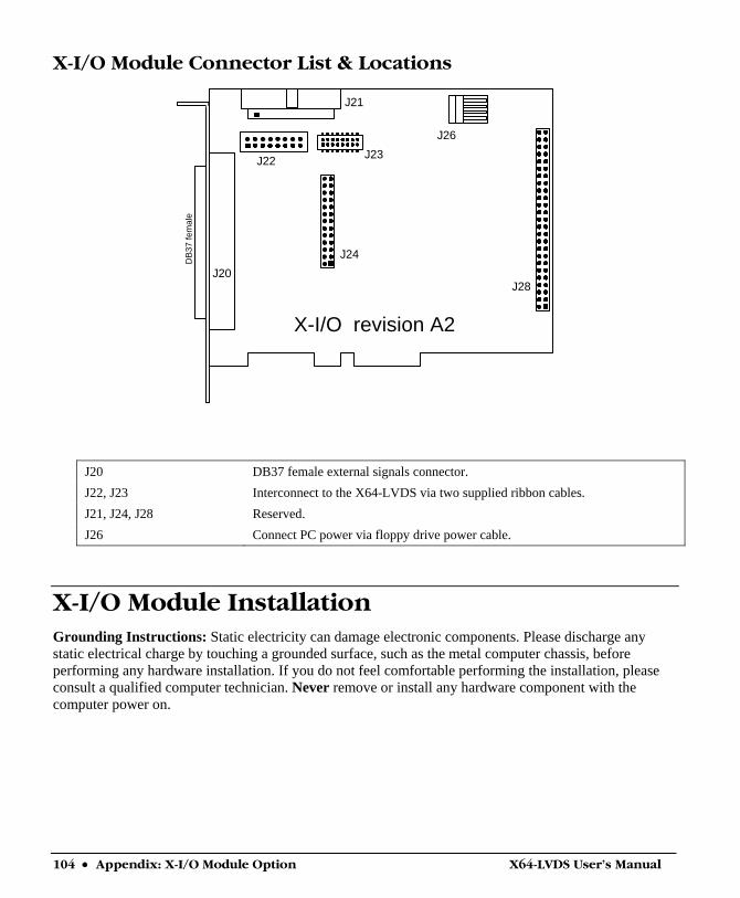
104 • Appendix: X-I/O Module Option X64-LVDS User's Manual
X-I/O Module Connector List & Locations
DB
37 fe
mal
e
J21
J22 J23
J24J20
J26
J28
X-I/O revision A2
J20 DB37 female external signals connector. J22, J23 Interconnect to the X64-LVDS via two supplied ribbon cables. J21, J24, J28 Reserved. J26 Connect PC power via floppy drive power cable.
X-I/O Module Installation Grounding Instructions: Static electricity can damage electronic components. Please discharge any static electrical charge by touching a grounded surface, such as the metal computer chassis, before performing any hardware installation. If you do not feel comfortable performing the installation, please consult a qualified computer technician. Never remove or install any hardware component with the computer power on.
X64-LVDS User's Manual Appendix: X-I/O Module Option • 105
Board Installation
Installing an X-I/O Module to an existing X64-LVDS installation takes only a few minutes. Install the X-I/O board into the host system as follows:
• Power off the computer system that has the installed X64-LVDS board. • Disconnect the external signals cable (OC-64CC-GIO25EM) if it was used. Remove that cable
bracket from the computer. • Insert the X-I/O module into any free PCI slot (no PCI electrical connections are used), securing
the bracket. • Connect the X-I/O module via 2 flat ribbon cables. Connect cable OC-64CC-F1616 from the
X64-LVDS J3 to the X-I/O J22. Connect cable OC-IO0C-ANLVDS from the X64-LVDS J5 to the X-I/O J23.
• Power on the computer again. • For new X64-LVDS and X-I/O module installations, simply follow the procedure to install
Sapera and the X64-LVDS driver (start with "Sapera LT Library Installation" on page 10).
X64-LVDS and X-I/O Driver Update • If both Sapera 5.30 and X64-LVDS driver 1.10 need to be installed, follow the procedure
"Upgrading Sapera or any DALSA Board Driver" on page 9. This procedure steps through the upgrade of both Sapera and the board driver—typically required when installing the X-I/O module in the field.
• If the X64-LVDS installation already has the required Sapera and board driver version, install the X-I/O module and perform a firmware update as described in "Executing the Firmware Loader from the Start Menu" on page 16.
X-I/O Module External Connections to the DB37 Users can assemble their interface cable, using some or all of the signals available on the X-I/O module DB37. Use a male DB37 with thumb screws for a secure fit. Wiring type should meet the needs of the imaging environment.
For the external signals Trigger Input, Shaft Encoder Input, and Strobe output, now available on the DB37, refer to "J3: External Signals Connector Block" on page 95 for signal details.
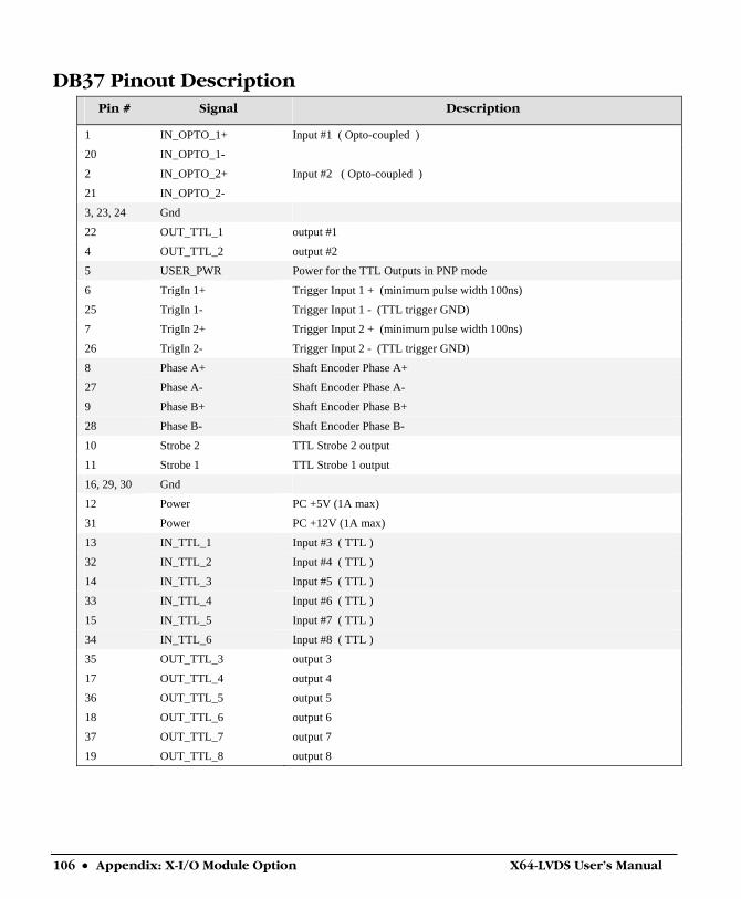
106 • Appendix: X-I/O Module Option X64-LVDS User's Manual
DB37 Pinout Description Pin # Signal Description
1 IN_OPTO_1+
20 IN_OPTO_1-
Input #1 ( Opto-coupled )
2 IN_OPTO_2+
21 IN_OPTO_2-
Input #2 ( Opto-coupled )
3, 23, 24 Gnd
22 OUT_TTL_1 output #1
4 OUT_TTL_2 output #2
5 USER_PWR Power for the TTL Outputs in PNP mode
6 TrigIn 1+ Trigger Input 1 + (minimum pulse width 100ns)
25 TrigIn 1- Trigger Input 1 - (TTL trigger GND)
7 TrigIn 2+ Trigger Input 2 + (minimum pulse width 100ns)
26 TrigIn 2- Trigger Input 2 - (TTL trigger GND)
8 Phase A+ Shaft Encoder Phase A+
27 Phase A- Shaft Encoder Phase A-
9 Phase B+ Shaft Encoder Phase B+
28 Phase B- Shaft Encoder Phase B-
10 Strobe 2 TTL Strobe 2 output
11 Strobe 1 TTL Strobe 1 output
16, 29, 30 Gnd
12 Power PC +5V (1A max)
31 Power PC +12V (1A max)
13 IN_TTL_1 Input #3 ( TTL )
32 IN_TTL_2 Input #4 ( TTL )
14 IN_TTL_3 Input #5 ( TTL )
33 IN_TTL_4 Input #6 ( TTL )
15 IN_TTL_5 Input #7 ( TTL )
34 IN_TTL_6 Input #8 ( TTL )
35 OUT_TTL_3 output 3
17 OUT_TTL_4 output 4
36 OUT_TTL_5 output 5
18 OUT_TTL_6 output 6
37 OUT_TTL_7 output 7
19 OUT_TTL_8 output 8
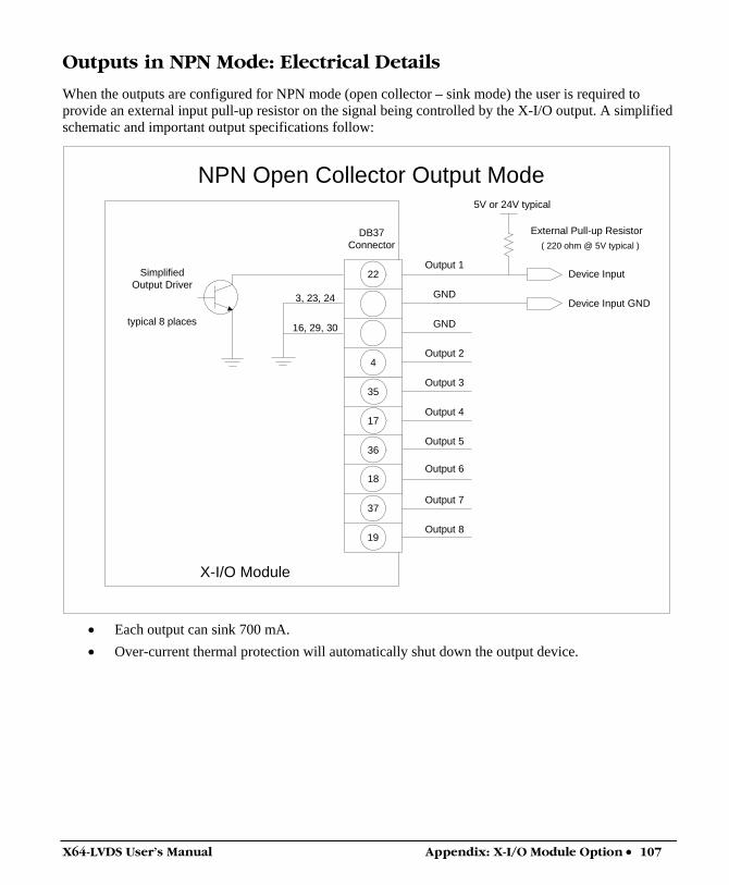
X64-LVDS User's Manual Appendix: X-I/O Module Option • 107
Outputs in NPN Mode: Electrical Details
When the outputs are configured for NPN mode (open collector – sink mode) the user is required to provide an external input pull-up resistor on the signal being controlled by the X-I/O output. A simplified schematic and important output specifications follow:
Output 1
Output 2
Output 3
Output 4
Output 5
Output 6
Output 7
Output 8
GND
GND
External Pull-up Resistor
Device Input
Device Input GND
DB37Connector
SimplifiedOutput Driver
typical 8 places
X-I/O Module
22
3, 23, 24
4
35
17
36
18
37
19
16, 29, 30
NPN Open Collector Output Mode5V or 24V typical
( 220 ohm @ 5V typical )
• Each output can sink 700 mA. • Over-current thermal protection will automatically shut down the output device.
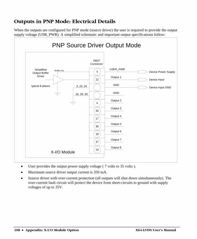
108 • Appendix: X-I/O Module Option X64-LVDS User's Manual
Outputs in PNP Mode: Electrical Details
When the outputs are configured for PNP mode (source driver) the user is required to provide the output supply voltage (USR_PWR). A simplified schematic and important output specifications follow:
Output 1
Output 2
Output 3
Output 4
Output 5
Output 6
Output 7
Output 8
GND
GND
Device Input
Device Input GND
DB37Connector
SimplifiedOutput Buffer
Driver
typical 8 places
X-I/O Module
22
3, 23, 24
4
35
17
36
18
37
19
16, 29, 30
PNP Source Driver Output Mode
Device Power SupplyUSER_PWR
5Buffer Vcc
• User provides the output power supply voltage ( 7 volts to 35 volts ). • Maximum source driver output current is 350 mA. • Source driver with over-current protection (all outputs will shut down simultaneously). The
over-current fault circuit will protect the device from short-circuits to ground with supply voltages of up to 35V.
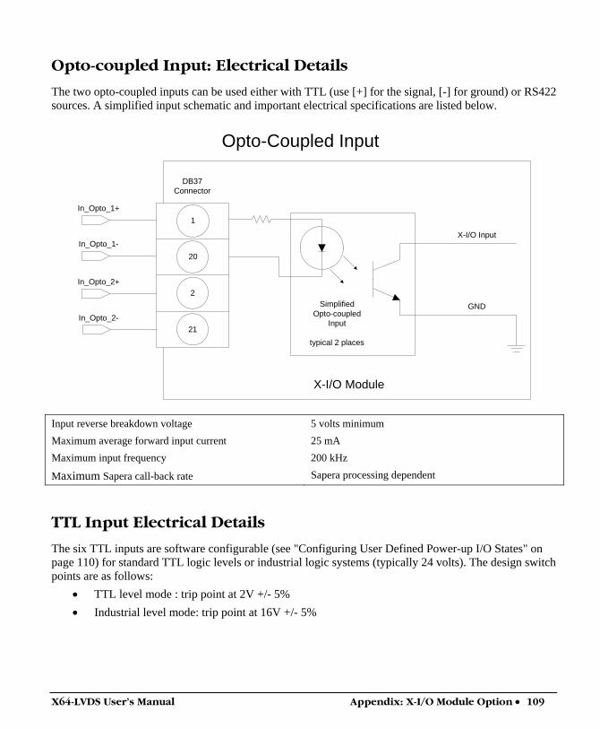
X64-LVDS User's Manual Appendix: X-I/O Module Option • 109
Opto-coupled Input: Electrical Details
The two opto-coupled inputs can be used either with TTL (use [+] for the signal, [-] for ground) or RS422 sources. A simplified input schematic and important electrical specifications are listed below.
X-I/O Input
GNDSimplifiedOpto-coupled
Input
typical 2 places
1
20
2
21
X-I/O Module
Opto-Coupled Input
DB37Connector
In_Opto_1+
In_Opto_1-
In_Opto_2+
In_Opto_2-
Input reverse breakdown voltage 5 volts minimum Maximum average forward input current 25 mA Maximum input frequency 200 kHz
Maximum Sapera call-back rate Sapera processing dependent
TTL Input Electrical Details
The six TTL inputs are software configurable (see "Configuring User Defined Power-up I/O States" on page 110) for standard TTL logic levels or industrial logic systems (typically 24 volts). The design switch points are as follows:
• TTL level mode : trip point at 2V +/- 5% • Industrial level mode: trip point at 16V +/- 5%
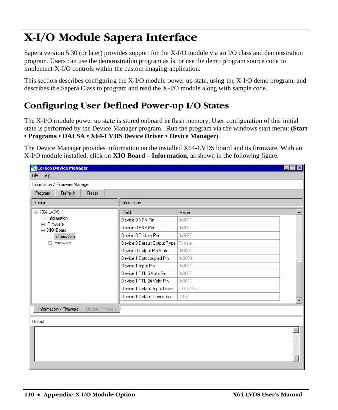
110 • Appendix: X-I/O Module Option X64-LVDS User's Manual
X-I/O Module Sapera Interface Sapera version 5.30 (or later) provides support for the X-I/O module via an I/O class and demonstration program. Users can use the demonstration program as is, or use the demo program source code to implement X-I/O controls within the custom imaging application.
This section describes configuring the X-I/O module power up state, using the X-I/O demo program, and describes the Sapera Class to program and read the X-I/O module along with sample code.
Configuring User Defined Power-up I/O States
The X-I/O module power up state is stored onboard in flash memory. User configuration of this initial state is performed by the Device Manager program. Run the program via the windows start menu: (Start • Programs • DALSA • X64-LVDS Device Driver • Device Manager).
The Device Manager provides information on the installed X64-LVDS board and its firmware. With an X-I/O module installed, click on XIO Board – Information, as shown in the following figure.
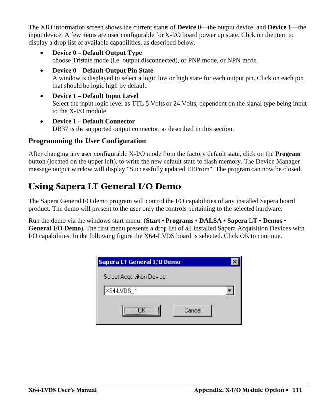
X64-LVDS User's Manual Appendix: X-I/O Module Option • 111
The XIO information screen shows the current status of Device 0—the output device, and Device 1—the input device. A few items are user configurable for X-I/O board power up state. Click on the item to display a drop list of available capabilities, as described below.
• Device 0 – Default Output Type choose Tristate mode (i.e. output disconnected), or PNP mode, or NPN mode.
• Device 0 – Default Output Pin State A window is displayed to select a logic low or high state for each output pin. Click on each pin that should be logic high by default.
• Device 1 – Default Input Level Select the input logic level as TTL 5 Volts or 24 Volts, dependent on the signal type being input to the X-I/O module.
• Device 1 – Default Connector DB37 is the supported output connector, as described in this section.
Programming the User Configuration
After changing any user configurable X-I/O mode from the factory default state, click on the Program button (located on the upper left), to write the new default state to flash memory. The Device Manager message output window will display "Successfully updated EEProm". The program can now be closed.
Using Sapera LT General I/O Demo
The Sapera General I/O demo program will control the I/O capabilities of any installed Sapera board product. The demo will present to the user only the controls pertaining to the selected hardware.
Run the demo via the windows start menu: (Start • Programs • DALSA • Sapera LT • Demos • General I/O Demo). The first menu presents a drop list of all installed Sapera Acquisition Devices with I/O capabilities. In the following figure the X64-LVDS board is selected. Click OK to continue.
112 • Appendix: X-I/O Module Option X64-LVDS User's Manual
General I/O Module Control Panel
The I/O module control demo presents the I/O capabilities of the installed hardware. The following figure shows the X-I/O module connected to the X64-LVDS board.
Output Pins: The first column displays the current state of the eight output pins (I/O Device #0). • The startup default state is user configured using the Device Manager program. • The state of each output can be changed by clicking on its status button. • Use the Signal Output drop menu to select the output mode (Tristate, PNP, NPN).
Input Pins: The second section provides input pin status (I/O device #1). Note that this program is a demo, therefore no action takes place on an input event.
• The first column reads the logic level present on each input. The Input Level drop menu changes the logic level from 5V TTL to 24V logic. Use the Device Manager program to select the default logic level type.
• The second column demonstrates activating interrupts on individual inputs. In this demo program, use the Enable box to activate the interrupt on an input. The Count box will tally detected input events. Use the Signal Event drop menu to select which input signal edge to detect. The Reset button clears all event counts.
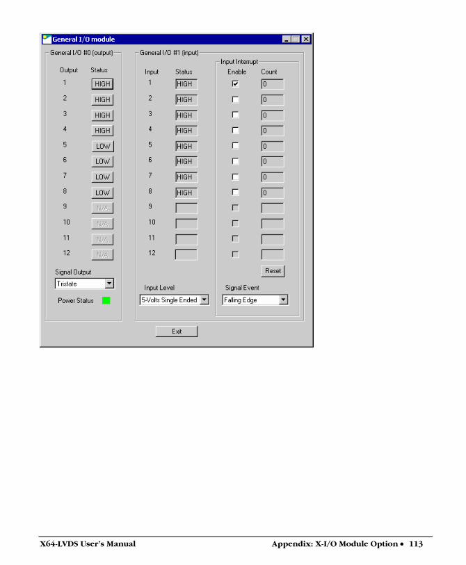
X64-LVDS User's Manual Appendix: X-I/O Module Option • 113
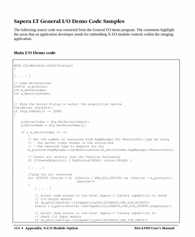
114 • Appendix: X-I/O Module Option X64-LVDS User's Manual
Sapera LT General I/O Demo Code Samples
The following source code was extracted from the General I/O demo program. The comments highlight the areas that an application developer needs for embedding X-I/O module controls within the imaging application.
Main I/O Demo code BOOL CGioMainDlg::OnInitDialog() { [ . . . ] // some declarations UINT32 m_gioCount; int m_ServerIndex; int m_ResourceIndex; // Show the Server Dialog to select the acquisition device CGioServer dlg(this); if (dlg.DoModal() == IDOK) { m_ServerIndex = dlg.GetServerIndex(); m_ServerName = dlg.GetServerName(); if ( m_ServerIndex != -1) { // Get the number of resources from SapManager for ResourceGio type by using // - the server index chosen in the dialog box // - the resource type to enquire for Gio m_gioCount=SapManager::GetResourceCount(m_ServerIndex,SapManager::ResourceGio); // Create all objects [see the function following] if (!CreateObjects()) { EndDialog(TRUE); return FALSE; } [ . . . ] //Loop for all resources for (UINT32 iDevice = 0; (iDevice < MAX_GIO_DEVICE) && (iDevice < m_gioCount); iDevice++) { [ . . . ] // direct read access to low-level Sapera C library capability to check // I/O Output module if (m_pGio[iDevice]->IsCapabilityValid(CORGIO_CAP_DIR_OUTPUT)) status = m_pGio[iDevice]->GetCapability(CORGIO_CAP_DIR_OUTPUT,&capOutput); // direct read access to low-level Sapera C library capability to // check I/O Input module if (m_pGio[iDevice]->IsCapabilityValid(CORGIO_CAP_DIR_INPUT))
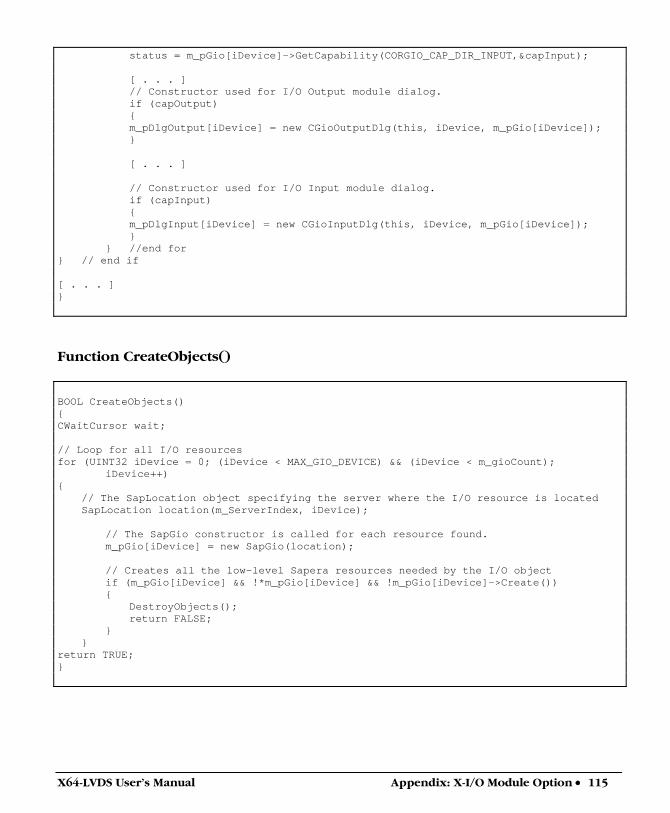
X64-LVDS User's Manual Appendix: X-I/O Module Option • 115
status = m_pGio[iDevice]->GetCapability(CORGIO_CAP_DIR_INPUT,&capInput); [ . . . ] // Constructor used for I/O Output module dialog. if (capOutput) { m_pDlgOutput[iDevice] = new CGioOutputDlg(this, iDevice, m_pGio[iDevice]); } [ . . . ] // Constructor used for I/O Input module dialog. if (capInput) { m_pDlgInput[iDevice] = new CGioInputDlg(this, iDevice, m_pGio[iDevice]); } } //end for } // end if [ . . . ] }
Function CreateObjects() BOOL CreateObjects() { CWaitCursor wait; // Loop for all I/O resources for (UINT32 iDevice = 0; (iDevice < MAX_GIO_DEVICE) && (iDevice < m_gioCount); iDevice++) { // The SapLocation object specifying the server where the I/O resource is located SapLocation location(m_ServerIndex, iDevice); // The SapGio constructor is called for each resource found. m_pGio[iDevice] = new SapGio(location); // Creates all the low-level Sapera resources needed by the I/O object if (m_pGio[iDevice] && !*m_pGio[iDevice] && !m_pGio[iDevice]->Create()) { DestroyObjects(); return FALSE; } } return TRUE; }
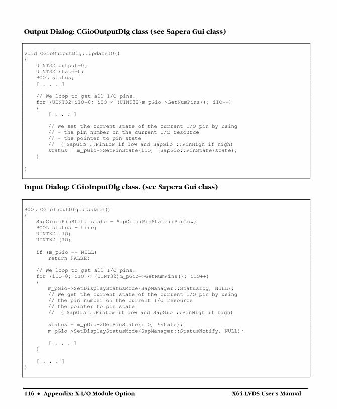
116 • Appendix: X-I/O Module Option X64-LVDS User's Manual
Output Dialog: CGioOutputDlg class (see Sapera Gui class) void CGioOutputDlg::UpdateIO() { UINT32 output=0; UINT32 state=0; BOOL status; [ . . . ] // We loop to get all I/O pins. for (UINT32 iIO=0; iIO < (UINT32)m_pGio->GetNumPins(); iIO++) { [ . . . ] // We set the current state of the current I/O pin by using // - the pin number on the current I/O resource // - the pointer to pin state // ( SapGio ::PinLow if low and SapGio ::PinHigh if high) status = m_pGio->SetPinState(iIO, (SapGio::PinState)state); } }
Input Dialog: CGioInputDlg class. (see Sapera Gui class) BOOL CGioInputDlg::Update() { SapGio::PinState state = SapGio::PinState::PinLow; BOOL status = true; UINT32 iIO; UINT32 jIO; if (m_pGio == NULL) return FALSE; // We loop to get all I/O pins. for (iIO=0; iIO < (UINT32)m_pGio->GetNumPins(); iIO++) { m_pGio->SetDisplayStatusMode(SapManager::StatusLog, NULL); // We get the current state of the current I/O pin by using // the pin number on the current I/O resource // the pointer to pin state // ( SapGio ::PinLow if low and SapGio ::PinHigh if high) status = m_pGio->GetPinState(iIO, &state); m_pGio->SetDisplayStatusMode(SapManager::StatusNotify, NULL); [ . . . ] } [ . . . ] }
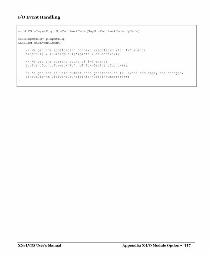
X64-LVDS User's Manual Appendix: X-I/O Module Option • 117
I/O Event Handling void CGioInputDlg::GioCallbackInfo(SapGioCallbackInfo *pInfo) { CGioInputDlg* pInputDlg; CString strEventCount; // We get the application context associated with I/O events pInputDlg = (CGioInputDlg*)pInfo->GetContext(); // We get the current count of I/O events strEventCount.Format("%d", pInfo->GetEventCount()); // We get the I/O pin number that generated an I/O event and apply the changes. pInputDlg->m_GioEventCount[pInfo->GetPinNumber()]++; }

118 • Appendix: X-I/O Module Option X64-LVDS User's Manual
X64-LVDS User's Manual DALSA Contact Information • 119
DALSA Contact Information
Sales Information Visit our web site: http://www.imaging.com/ Email: mailto:[email protected]
Canada/International
DALSA Montreal 7075 Place Robert-Joncas Suite #142 St. Laurent, Quebec H4M 2Z2 Canada
Tel: (514) 333-1301 Fax: (514) 333-1388
US Sales Office
DALSA 700 Technology Park Drive Billerica, Ma. 01821
Tel: (978) 670-2000 Fax: (978) 670-2010
Asia Sales Office
DALSA Asia Pacific Ikebukuro East 13F 3-4-3 Higashi Ikebukuro, Toshima-ku, Tokyo Japan
Tel: +81 3 5960 6353 Fax: +81 3 5960 6354

120 • DALSA Contact Information X64-LVDS User's Manual
Technical Support
Any support question or request can be submitted via our web site:
Technical support form via our web page: Support requests for imaging product installations, Support requests for imaging applications
http://www.imaging.com/support
Camera support information http://www.imaging.com/camsearch Product literature and driver updates http://www.imaging.com/download
X64-LVDS User's Manual Glossary of Terms • 121
Glossary of Terms
Bandwidth
Describes the measure of data transfer capacity. PCI devices must share the maximum PCI bus bandwidth when transferring data to and from system memory or other devices.
CAM
Sapera camera file that uses the file extension CCA by default. Files using the CCA extension, also called CAM files (CORECO CAMERA files), contain all parameters which describe the camera video signal characteristics and operation modes (i.e. what the camera outputs).
Channel
Camera data path that includes all parts of a video line.
Checksum
A value used to ensure data is stored without error. It is created by calculating the binary values in a block of data using some algorithm and storing the results with the data.
CMI
Client Modification Instruction. A client requested engineering change applied to a DALSA board product to support either a non-standard function or custom camera.
Contiguous memory
A block of physical memory, occupying consecutive addresses.
CRC
Proprietary Sapera raw image data file format that supports any Sapera buffer type and utilizes an informative file header. Refer to the Sapera Basic Modules Reference Manual “Buffer File Formats” section.
Firmware
Software such as a board driver that is stored in nonvolatile memory mounted on that board.
Frame buffer
An area of memory used to hold a frame of image data. A frame buffer may exist on the acquisition hardware or be allocated by the acquisition hardware device driver in host system memory.
122 • Glossary of Terms X64-LVDS User's Manual
Grab
Acquiring an image frame by means of a frame grabber.
Host
Refers to the computer system that supports the installed frame grabber.
Host buffer
Refers to a frame buffer allocated in the physical memory of the host computer system.
LSB
Least Significant Bit in a binary data word.
MSB
Most Significant Bit in a binary data word.
PCI 32
Peripheral Component Interconnect. The PCI local bus is a 32-bit high-performance expansion bus intended for interconnecting add-in boards, controllers, and processor/memory systems.
PCI 64
A superset of the PCI specification providing a 64 bit data path and a 66 MHz clock.
Pixel
Picture Element. The number of pixels describes the number of digital samples taken of the analog video signal. The number of pixels per video line by the number of active video lines describes the acquisition image resolution. The binary size of each pixel (i.e., 8-bits, 15-bits, 24-bits) defines the number of gray levels or colors possible for each pixel.
RAW
A Sapera data file format where there is no header information and that supports any Sapera buffer type. Refer to the Sapera Basic Modules Reference Manual “Buffer File Formats” section.
X64-LVDS User's Manual Glossary of Terms • 123
Scatter Gather
Host system memory allocated for frame buffers that is virtually contiguous but physically scattered throughout all available memory.
Tap
Data path from a camera that includes a part of or whole video line. When a camera tap outputs a partial video line, the multiple camera tap data must be constructed by combining the data in the correct order.
VIC
Sapera camera parameter definition file that uses the file extension CVI by default. Files using the CVI extension, also know as VIC files (CORECO VIDEO files), contain all operating parameters related to the frame grabber board (i.e. what the frame grabber can actually do with camera controls or incoming video).

124 • Glossary of Terms X64-LVDS User's Manual
X64-LVDS User's Manual Index • 125
Index
A About Sapera LT 5 acquisition parameters 43 administrator 9, 10 AUTORUN 10
B BoardInfo.txt 20, 38 boot failure 37 boot recovery mode 38 buffer count 46
C C++ class library 5 cable diagrams 23 calibration information 39 camera connections 24 Camera file 43, 51, 53 camera serial port control 17 CamExpert 43, 51, 53 Certifications 77 configuration switch 38 connector location 104 Contiguous Memory 21 CORACQ_CAP_BIT_ORDERING 69 CORACQ_CAP_CAM_RESET 65 CORACQ_CAP_CAM_RESET_DURATION_MAX 65 CORACQ_CAP_CAM_RESET_DURATION_MIN 65 CORACQ_CAP_CAM_RESET_METHOD 65 CORACQ_CAP_CAM_RESET_POLARITY 65 CORACQ_CAP_CAM_TRIGGER 65 CORACQ_CAP_CAM_TRIGGER_DURATION_MAX 65 CORACQ_CAP_CAM_TRIGGER_DURATION_MIN 65 CORACQ_CAP_CAM_TRIGGER_METHOD 65 CORACQ_CAP_CAM_TRIGGER_POLARITY 65 CORACQ_CAP_CAMSEL_MONO 69 CORACQ_CAP_CAMSEL_RGB 69 CORACQ_CAP_CHANNEL 65
CORACQ_CAP_CHANNELS_ORDER 65 CORACQ_CAP_CROP_HEIGHT_MAX 69 CORACQ_CAP_CROP_HEIGHT_MIN 69 CORACQ_CAP_CROP_HEIGHT_MULT 69 CORACQ_CAP_CROP_HORZ 69 CORACQ_CAP_CROP_LEFT_MAX 69 CORACQ_CAP_CROP_LEFT_MIN 69 CORACQ_CAP_CROP_LEFT_MULT 69 CORACQ_CAP_CROP_TOP_MAX 69 CORACQ_CAP_CROP_TOP_MIN 69 CORACQ_CAP_CROP_TOP_MULT 69 CORACQ_CAP_CROP_VERT 69 CORACQ_CAP_CROP_WIDTH_MAX 69 CORACQ_CAP_CROP_WIDTH_MIN 69 CORACQ_CAP_CROP_WIDTH_MULT 69 CORACQ_CAP_DATA_VALID_ENABLE 65 CORACQ_CAP_DATA_VALID_POLARITY 65 CORACQ_CAP_DETECT_HACTIVE 72 CORACQ_CAP_DETECT_VACTIVE 72 CORACQ_CAP_EVENT_TYPE 72 CORACQ_CAP_EXT_FRAME_TRIGGER 69 CORACQ_CAP_EXT_FRAME_TRIGGER_DETECTION 69 CORACQ_CAP_EXT_FRAME_TRIGGER_LEVEL 69 CORACQ_CAP_EXT_LINE_TRIGGER 69 CORACQ_CAP_EXT_LINE_TRIGGER_DETECTION 69 CORACQ_CAP_EXT_LINE_TRIGGER_LEVEL 69 CORACQ_CAP_EXT_LINE_TRIGGER_SOURCE 69 CORACQ_CAP_EXT_TRIGGER 69 CORACQ_CAP_EXT_TRIGGER_DETECTION 69 CORACQ_CAP_EXT_TRIGGER_DURATION_MAX 70 CORACQ_CAP_EXT_TRIGGER_DURATION_MIN 70 CORACQ_CAP_EXT_TRIGGER_FRAME_COUNT 69 CORACQ_CAP_EXT_TRIGGER_LEVEL 70 CORACQ_CAP_EXT_TRIGGER_SOURCE 70 CORACQ_CAP_FIELD_ORDER 65 CORACQ_CAP_FRAME 65 CORACQ_CAP_FRAME_LENGTH 70 CORACQ_CAP_HACTIVE_MAX 65 CORACQ_CAP_HACTIVE_MIN 65 CORACQ_CAP_HACTIVE_MULT 66 CORACQ_CAP_HBACK_INVALID_MAX 66 CORACQ_CAP_HBACK_INVALID_MIN 66 CORACQ_CAP_HBACK_INVALID_MULT 66 CORACQ_CAP_HFRONT_INVALID_MAX 66 CORACQ_CAP_HFRONT_INVALID_MIN 66 CORACQ_CAP_HFRONT_INVALID_MULT 66
126 • Index X64-LVDS User's Manual
CORACQ_CAP_HSYNC_MAX 66 CORACQ_CAP_HSYNC_MIN 66 CORACQ_CAP_HSYNC_MULT 66 CORACQ_CAP_HSYNC_POLARITY 66 CORACQ_CAP_HSYNC_REF 70 CORACQ_CAP_INT_FRAME_TRIGGER 70 CORACQ_CAP_INT_FRAME_TRIGGER_FREQ_MAX 70 CORACQ_CAP_INT_FRAME_TRIGGER_FREQ_MIN 70 CORACQ_CAP_INT_LINE_TRIGGER 70 CORACQ_CAP_INTERFACE 66 CORACQ_CAP_LINE_INTEGRATE 66 CORACQ_CAP_LINE_INTEGRATE_DURATION_MAX 70 CORACQ_CAP_LINE_INTEGRATE_DURATION_MIN 70 CORACQ_CAP_LINE_INTEGRATE_METHOD 66 CORACQ_CAP_LINE_INTEGRATE_PULSE0_DELAY_MAX 66 CORACQ_CAP_LINE_INTEGRATE_PULSE0_DELAY_MIN 66 CORACQ_CAP_LINE_INTEGRATE_PULSE0_DURATION_MAX 66 CORACQ_CAP_LINE_INTEGRATE_PULSE0_DURATION_MIN 66 CORACQ_CAP_LINE_INTEGRATE_PULSE0_POLARITY 66 CORACQ_CAP_LINE_INTEGRATE_PULSE1_DELAY_MAX 66 CORACQ_CAP_LINE_INTEGRATE_PULSE1_DELAY_MIN 66 CORACQ_CAP_LINE_INTEGRATE_PULSE1_DURATION_MAX 66 CORACQ_CAP_LINE_INTEGRATE_PULSE1_DURATION_MIN 66 CORACQ_CAP_LINE_INTEGRATE_PULSE1_POLARITY 66 CORACQ_CAP_LINE_TRIGGER 66 CORACQ_CAP_LINE_TRIGGER_DELAY_MAX 66 CORACQ_CAP_LINE_TRIGGER_DELAY_MIN 66 CORACQ_CAP_LINE_TRIGGER_DURATION_MAX 66 CORACQ_CAP_LINE_TRIGGER_DURATION_MIN 66 CORACQ_CAP_LINE_TRIGGER_METHOD 66 CORACQ_CAP_LINE_TRIGGER_POLARITY 66 CORACQ_CAP_LINESCAN_DIRECTION 67 CORACQ_CAP_LINESCAN_DIRECTION_POLARITY 67 CORACQ_CAP_LUT 70 CORACQ_CAP_LUT_ENABLE 70
CORACQ_CAP_OUTPUT_FORMAT 70 CORACQ_CAP_OUTPUT_FORMAT_BYTE_MULT 70 CORACQ_CAP_PIXEL_CLK_DETECTION 67 CORACQ_CAP_PIXEL_CLK_EXT_MAX 67 CORACQ_CAP_PIXEL_CLK_EXT_MIN 67 CORACQ_CAP_PIXEL_CLK_INT_MAX 67 CORACQ_CAP_PIXEL_CLK_INT_MIN 67 CORACQ_CAP_PIXEL_CLK_SRC 67 CORACQ_CAP_PIXEL_DEPTH 67 CORACQ_CAP_PIXEL_DEPTH_PER_TAP 67 CORACQ_CAP_SCALE_HORZ_METHOD 70 CORACQ_CAP_SCALE_VERT_METHOD 70 CORACQ_CAP_SCAN 67 CORACQ_CAP_SHAFT_ENCODER 70 CORACQ_CAP_SHAFT_ENCODER_DROP 70 CORACQ_CAP_SHAFT_ENCODER_DROP_MAX 70 CORACQ_CAP_SHAFT_ENCODER_DROP_MIN 70 CORACQ_CAP_SHAFT_ENCODER_ENABLE 70 CORACQ_CAP_SHAFT_ENCODER_LEVEL 70 CORACQ_CAP_SIGNAL 67 CORACQ_CAP_SIGNAL_STATUS 72 CORACQ_CAP_SOFTWARE_TRIGGER 72 CORACQ_CAP_STROBE 70 CORACQ_CAP_STROBE_DELAY_2_MAX 70 CORACQ_CAP_STROBE_DELAY_2_MIN 70 CORACQ_CAP_STROBE_DELAY_MAX 70 CORACQ_CAP_STROBE_DELAY_MIN 70 CORACQ_CAP_STROBE_DURATION_MAX 70 CORACQ_CAP_STROBE_DURATION_MIN 70 CORACQ_CAP_STROBE_LEVEL 70 CORACQ_CAP_STROBE_METHOD 70 CORACQ_CAP_STROBE_POLARITY 71 CORACQ_CAP_SYNC 67 CORACQ_CAP_SYNC_CROP_HEIGHT_MAX 71 CORACQ_CAP_SYNC_CROP_HEIGHT_MIN 71 CORACQ_CAP_SYNC_CROP_HEIGHT_MULT 71 CORACQ_CAP_SYNC_CROP_LEFT_MAX 71 CORACQ_CAP_SYNC_CROP_LEFT_MIN 71 CORACQ_CAP_SYNC_CROP_LEFT_MULT 71 CORACQ_CAP_SYNC_CROP_TOP_MAX 71 CORACQ_CAP_SYNC_CROP_TOP_MIN 71 CORACQ_CAP_SYNC_CROP_TOP_MULT 71 CORACQ_CAP_SYNC_CROP_WIDTH_MAX 71 CORACQ_CAP_SYNC_CROP_WIDTH_MIN 71 CORACQ_CAP_SYNC_CROP_WIDTH_MULT 71 CORACQ_CAP_TAP_DIRECTION 67 CORACQ_CAP_TAP_OUTPUT 67 CORACQ_CAP_TAPS 67 CORACQ_CAP_TIME_INTEGRATE 67
X64-LVDS User's Manual Index • 127
CORACQ_CAP_TIME_INTEGRATE_DELAY_MAX 71 CORACQ_CAP_TIME_INTEGRATE_DELAY_MIN 71 CORACQ_CAP_TIME_INTEGRATE_DURATION_MAX 71 CORACQ_CAP_TIME_INTEGRATE_DURATION_MIN 71 CORACQ_CAP_TIME_INTEGRATE_METHOD 68 CORACQ_CAP_TIME_INTEGRATE_PULSE0_DELAY_MAX 68 CORACQ_CAP_TIME_INTEGRATE_PULSE0_DELAY_MIN 68 CORACQ_CAP_TIME_INTEGRATE_PULSE0_DURATION_MAX 68 CORACQ_CAP_TIME_INTEGRATE_PULSE0_DURATION_MIN 68 CORACQ_CAP_TIME_INTEGRATE_PULSE0_POLARITY 68 CORACQ_CAP_TIME_INTEGRATE_PULSE1_DELAY_MAX 68 CORACQ_CAP_TIME_INTEGRATE_PULSE1_DELAY_MIN 68 CORACQ_CAP_TIME_INTEGRATE_PULSE1_DURATION_MAX 68 CORACQ_CAP_TIME_INTEGRATE_PULSE1_DURATION_MIN 68 CORACQ_CAP_TIME_INTEGRATE_PULSE1_POLARITY 68 CORACQ_CAP_VACTIVE_MAX 68 CORACQ_CAP_VACTIVE_MIN 68 CORACQ_CAP_VACTIVE_MULT 68 CORACQ_CAP_VBACK_INVALID_MAX 68 CORACQ_CAP_VBACK_INVALID_MIN 68 CORACQ_CAP_VBACK_INVALID_MULT 68 CORACQ_CAP_VFRONT_INVALID_MAX 68 CORACQ_CAP_VFRONT_INVALID_MIN 68 CORACQ_CAP_VFRONT_INVALID_MULT 68 CORACQ_CAP_VIDEO 68 CORACQ_CAP_VIDEO_STD 68 CORACQ_CAP_VSYNC_MAX 68 CORACQ_CAP_VSYNC_MIN 68 CORACQ_CAP_VSYNC_MULT 68 CORACQ_CAP_VSYNC_POLARITY 68 CORACQ_CAP_VSYNC_REF 71 CORACQ_PRM_EXT_LINE_TRIGGER_DETECTION 96 CORACQ_PRM_EXT_LINE_TRIGGER_ENABLE 96 CORACQ_PRM_EXT_LINE_TRIGGER_LEVEL 96 CORACQ_PRM_EXT_LINE_TRIGGER_SOURCE 96
CORACQ_PRM_EXT_TRIGGER_DETECTION 96 CORACQ_PRM_EXT_TRIGGER_ENABLE 96 CORACQ_PRM_EXT_TRIGGER_LEVEL 96 CORACQ_PRM_SHAFT_ENCODER_DROP 96 CORACQ_PRM_SHAFT_ENCODER_ENABLE 96 CORACQ_PRM_SHAFT_ENCODER_LEVEL 96 CORACQ_PRM_STROBE_DELAY 96 CORACQ_PRM_STROBE_DURATION 96 CORACQ_PRM_STROBE_ENABLE 96 CORACQ_PRM_STROBE_LEVEL 96 CORACQ_PRM_STROBE_METHOD 96 CORACQ_PRM_STROBE_POLARITY 96 CORACQ_VAL_CAM_TRIGGER_METHOD_1 55, 56, 62 CORACQ_VAL_LINE_INTEGRATE_METHOD_1 56 CORACQ_VAL_LINE_INTEGRATE_METHOD_2 57 CORACQ_VAL_LINE_INTEGRATE_METHOD_3 57 CORACQ_VAL_LINE_INTEGRATE_METHOD_4 58 CORACQ_VAL_LINE_TRIGGER_METHOD_1 58 CORACQ_VAL_STROBE_METHOD_1 62 CORACQ_VAL_STROBE_METHOD_2 63 CORACQ_VAL_STROBE_METHOD_3 63 CORACQ_VAL_STROBE_METHOD_4 64 CORACQ_VAL_TIME_INTEGRATE_METHOD_1 59 CORACQ_VAL_TIME_INTEGRATE_METHOD_2 59 CORACQ_VAL_TIME_INTEGRATE_METHOD_3 59 CORACQ_VAL_TIME_INTEGRATE_METHOD_4 60 CORACQ_VAL_TIME_INTEGRATE_METHOD_5 60 CORACQ_VAL_TIME_INTEGRATE_METHOD_6 61 CORACQ_VAL_TIME_INTEGRATE_METHOD_7 61
D DALSA Device Manager 38 DB25 female connector 97 debounce circuit time constant 99 Device Manager 15, 20, 110 Digital Signature 11, 12 driver upgrade 9
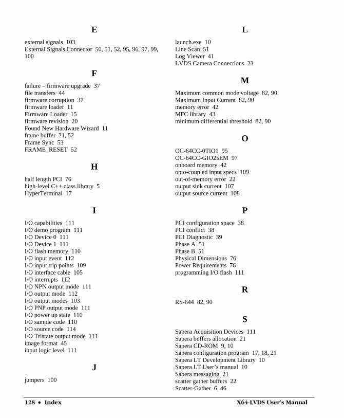
128 • Index X64-LVDS User's Manual
E external signals 103 External Signals Connector 50, 51, 52, 95, 96, 97, 99, 100
F failure – firmware upgrade 37 file transfers 44 firmware corruption 37 firmware loader 11 Firmware Loader 15 firmware revision 20 Found New Hardware Wizard 11 frame buffer 21, 52 Frame Sync 53 FRAME_RESET 52
H half length PCI 76 high-level C++ class library 5 HyperTerminal 17
I I/O capabilities 111 I/O demo program 111 I/O Device 0 111 I/O Device 1 111 I/O flash memory 110 I/O input event 112 I/O input trip points 109 I/O interface cable 105 I/O interrupts 112 I/O NPN output mode 111 I/O output mode 112 I/O output modes 103 I/O PNP output mode 111 I/O power up state 110 I/O sample code 110 I/O source code 114 I/O Tristate output mode 111 image format 45 input logic level 111
J jumpers 100
L launch.exe 10 Line Scan 51 Log Viewer 41 LVDS Camera Connections 23
M Maximum common mode voltage 82, 90 Maximum Input Current 82, 90 memory error 42 MFC library 43 minimum differential threshold 82, 90
O OC-64CC-0TIO1 95 OC-64CC-GIO25EM 97 onboard memory 42 opto-coupled input specs 109 out-of-memory error 22 output sink current 107 output source current 108
P PCI configuration space 38 PCI conflict 38 PCI Diagnostic 39 Phase A 51 Phase B 51 Physical Dimensions 76 Power Requirements 76 programming I/O flash 111
R RS-644 82, 90
S Sapera Acquisition Devices 111 Sapera buffers allocation 21 Sapera CD-ROM 9, 10 Sapera configuration program 17, 18, 21 Sapera LT Development Library 10 Sapera LT User’s manual 10 Sapera messaging 21 scatter gather buffers 22 Scatter-Gather 6, 46
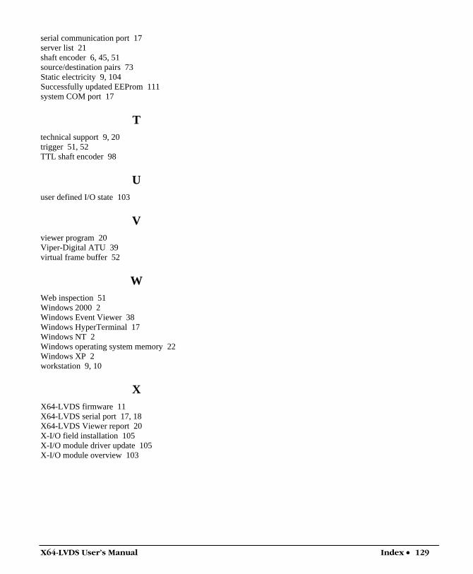
X64-LVDS User's Manual Index • 129
serial communication port 17 server list 21 shaft encoder 6, 45, 51 source/destination pairs 73 Static electricity 9, 104 Successfully updated EEProm 111 system COM port 17
T technical support 9, 20 trigger 51, 52 TTL shaft encoder 98
U user defined I/O state 103
V viewer program 20 Viper-Digital ATU 39 virtual frame buffer 52
W Web inspection 51 Windows 2000 2 Windows Event Viewer 38 Windows HyperTerminal 17 Windows NT 2 Windows operating system memory 22 Windows XP 2 workstation 9, 10
X X64-LVDS firmware 11 X64-LVDS serial port 17, 18 X64-LVDS Viewer report 20 X-I/O field installation 105 X-I/O module driver update 105 X-I/O module overview 103