wireless sensor network
DESCRIPTION
Design and development of wireless sensor network / Home Automation system using ZigbeeTRANSCRIPT
DESIGN AND DEVELOPMENT OF WIRELESS SENSOR NETWORK
A Major Project
Submitted in Partial Fulfillment of the Requirements For the Degree of
Bachelor OF TECHNOLOGY IN
ELECTRONICS & COMMUNICATION
ENGINEERING By
Rupam Patel and Akash Patel [06BEC109] [06BEC063]
Under the Guidance of
Prof. Mehul R. Naik
Department of Electrical Engineering Electronics & Communication Engineering Program
Institute of Technology, NIRMA UNIVERSITY AHMEDABAD 382 481
May 2010
II
Institute of Technology Department of Electrical Engineering
Electronics and Communication Branch
CERTIFICATE This is to certify that the Major Project Report entitled “Wireless Sensor
Network” submitted by Rupam Patel (Roll No. 06BEC109) & Akash Patel
(Roll No. 06BEC063) as the partial fulfillment of the requirements for the
award of the degree of Bachelor of Technology in Electronics &
Communication Engineering, Institute of Technology, Nirma University is the
record of work carried out by them under my supervision and guidance. The
work submitted in our opinion has reached a level required for being accepted
for the examination.
Date:
Prof. Mehul R. Naik Prof. A. S. Ranade (Project Guide) Head of Department Assistant Professor Electrical Engineering Electronics and Communication Institute of Technology Institute of Technology Nirma University Nirma University

III
ACKNOWLEDGEMENTS
We thank the Electronics and Communication Department, Institute of Technology, Nirma
University for giving us an opportunity to carry out this project work.
Apart from our efforts, the success of this project depends largely on the encouragement and
guidance of several other important individuals. We take this opportunity to express my
gratitude towards these people who have been instrumental in the successful completion of
this project.
We would like to convey our heart-felt gratitude to our project guide, Prof. Mehul R. Naik.
Sir, we thank you for allowing us to work on this project under your guidance. Your valuable
time, your technical expertise and most importantly, constant encouragement and motivation
in all the stages of the project was something for which we cannot thank you enough.
Our sincere thanks are also to Prof. A. S. Ranade, Head of the Department of EC
Engineering, Institute Of Technology, Nirma University, Ahmedabad for his co-operation
and motivation during our study.
We are highly indebted to God and to our family members by whose blessings, we are able to
complete our report. And also very thankful to all our friends for their help at all different
stages and whom we shared very intimate relationship.
THANK YOU.

IV
ABSTRACT Networks of wireless sensor devices are being deployed to collectively monitor and
disseminate information about a variety of phenomena of interest. Wireless networks have
changed the way we look at computing. Unlike the concept of reactive computing, these
networks usher in proactive computing by using intelligent sensors called ‘motes’ or ‘nodes’.
Unlike standard networking gear, wireless sensors can reorganize themselves to form a
network and convey meaningful data. These motes have the capability to reorganize
themselves into a network and transmit data that can range from measuring light,
temperature, humidity or even motion. Communication of signals is carried out using radio
frequency (RF) waves. The main advantages of wireless systems over wired systems is the
considerable reduction in the cost and power consumption. One can envisage a future where
we would be living in a world surrounded by embedded computers that anticipate human
need and act proactively.
Wireless Sensor Network is a subject still under research across all over the world. Now-a-
days there has been advancements in this field with smaller size and portability. We have
attempted to use the newly derived ZigBee protocol for the development of our project.
ZigBee provides low power wireless support with reasonable range of around 400 m. The
main part of the project is the base station which is equipped with the USB support for
communication with PC to access the data sent or received by the ZigBee module. The end
device is also equipped with same ZigBee module to accommodate the data transfer. The
form of data communicating between the devices is Analog as well as Digital. The power
consumption in the ZigBee module is so less that the device can run for months without
changing the batteries. This makes the application more versatile to use in harsh conditions
and in rural places. The PCBs are made with utmost accuracy and optimization of the
component placing. Due to the complexity of the circuits, the PCBs are made in industries
with PTH (Plated Through Hole) technology and SMD (Surface Mounting Device)
components, which ensure the reliability and optimization.
The main purpose of the project is the optimization of power as well as design parameters

V
Contents LIST OF FIGURES .............................................................................................................. III
LIST OF TABLES ................................................................................................................ IV
1 INTRODUCTION ............................................................................................................. 2
1.1 OVERVIEW OF WIRELESS SENSOR NETWORKS .............................................................. 3 1.2 MODELLING OF WIRELESS SENSOR NETWORKS ............................................................ 4 1.3 CHALLENGES ................................................................................................................. 6 1.4 OBJECTIVE OF THE PROJECT .......................................................................................... 7
2 PRIOR STUDIES .............................................................................................................. 9
2.1 CROSS-BOW SENSOR NETWORK KIT ............................................................................. 10 2.1.1 Robust Mesh Network .......................................................................................... 11
2.2 ARDUINO [5] ................................................................................................................. 11 2.2.1 Features ............................................................................................................... 12 2.2.2 Software ............................................................................................................... 12 2.2.3 Overview of the hardware used for study ............................................................ 13 2.2.4 Bootloader [6] ....................................................................................................... 14
3 HARDWARE DESCRIPTION ...................................................................................... 15
3.1 HARDWARE REQUIREMENTS ....................................................................................... 17 3.2 BLOCK DIAGRAM ........................................................................................................ 17
3.2.1 Base Station ......................................................................................................... 17 3.2.2 Remote Sensor Node ............................................................................................ 18
3.3 HARDWARE COMPONENTS .......................................................................................... 20 3.3.1 XBee RF Module [7] .............................................................................................. 20 3.3.2 Atmega168 Microcontroller [8] ............................................................................ 25 3.3.3 FT232R USB - UART Bridge Converter IC [9] .................................................... 27
3.4 MISCELLANEOUS HARDWARE PARTS: ......................................................................... 29 3.5 PROTOCOLS ................................................................................................................. 29
3.5.1 ZigBee (IEEE 802.15.4) ....................................................................................... 29 3.5.2 USB [13] Protocol ................................................................................................. 32
4 PRINTED CIRCUIT BOARD DESIGN ....................................................................... 33
4.1 INTRODUCTION TO PCB DESIGN USING EAGLE 5.7.0 ................................................... 34 4.2 FEATURES OF EAGLE 5.7.0 .......................................................................................... 34 4.3 INITIAL DESIGN OF WIRELESS NODE ........................................................................... 35 4.4 GENERATING GERBER FILES ........................................................................................ 37
5 COMMUNICATION INTERFACE ............................................................................. 38
5.1 SERIAL COMMUNICATION AND USB INTERFACE USING FT232R ................................ 39 5.2 CONFIGURING FT232R ................................................................................................ 41
5.2.1 Driver Installation ............................................................................................... 41 5.2.2 FTDI Configuration ............................................................................................. 44
5.3 WIRELESS COMMUNICATION USING IEEE 802.15.4 XBEE MODULE ........................... 45 5.3.1 Configuring XBEE ............................................................................................... 45
5.4 UNIVERSAL ASYNCHRONOUS RECEIVER TRANSMITTER (UART) INTERFACE ............. 47 5.4.1 Transmitting and receiving serial data ................................................................ 48
VI
5.4.2 Asynchronous receiving and transmitting ........................................................... 49
6 SOFTWARE INTERFACE ........................................................................................... 52
6.1 COMPILER AND SIMULATION SOFTWARE ..................................................................... 53 6.1.1 NetBeans IDE 6.8: [10] ......................................................................................... 53
6.2 INTERFACING HARDWARE VIA NETBEANS .................................................................. 55
7 APPLICATIONS ............................................................................................................. 58
7.1 APPLICATIONS ............................................................................................................. 59
8 RESULTS AND CONCLUSION ................................................................................... 63
REFERENCES ....................................................................................................................... 63
APPENDIX A ......................................................................................................................... 67
APPENDIX B ....................................................................................................................... 630
APPENDIX C ......................................................................................................................... 75
APPENDIX D ......................................................................................................................... 76
APPENDIX E ......................................................................................................................... 77
LIST OF FIGURES
VII
FIGURE 1-1 MODEL FOR DEPLOYMENT OF SENSORS IN A WIRELESS SENSOR NETWORK ............ 5 FIGURE 3-1 WIRELESS SENSOR NODE COMPONENT LAYOUT .................................................. 16 FIGURE 3-2 BLOCK DIAGRAM FOR BASE STATION................................................................... 18 FIGURE 3-3 BLOCK DIAGRAM OF AD HOC WIRELESS SENSOR NODE ........................................ 19 FIGURE 3-4 XBEE MODULE .................................................................................................... 20 FIGURE 3-5 ATMEGA168 ARCHITECTURE ................................................................................ 25 FIGURE 3-6 DIAGRAM OF FT232R IC ...................................................................................... 27 FIGURE 3-7 PROTOCOL STACK OF ZIGBEE ............................................................................... 30 FIGURE 4-1 INITIAL DESIGN OF NODE ....................................................................................... 35 FIGURE 4-2 INITIAL DESIGN-2 .................................................................................................. 35 FIGURE 4-3 DESIGN AFTER ROUTING SIGNALS .......................................................................... 35 FIGURE 4-4 NEW CIRCULAR DESIGN ......................................................................................... 35 FIGURE 4-5 AFTER ROUTING SIGNALS ...................................................................................... 36 FIGURE 4-6 FINAL OPTIMIZED LAYOUT DSIGN ......................................................................... 36 FIGURE 4-7 GENERATING GERBER FILES USING CAM PROCESSOR IN EAGLE 5.7.0 .................. 37 FIGURE 5-1 BASIC CONNECTIONS OF FTDI TO CONTROLLER ................................................... 39 FIGURE 5-2 POP-UP WINDOW IN WINDOWS .............................................................................. 42 FIGURE 5-3 INSTALLING FTDI DRIVERS ................................................................................... 42 FIGURE 5-4 DRIVER INSTALLATION FINISHED, NEW VIRTUAL COM PORT CREATED ................ 43 FIGURE 5-5 DEVICE MANAGER ................................................................................................. 43 FIGURE 5-6 CONFIGURING FT232R USING FT PROG SOFTWARE ............................................. 44 FIGURE 5-7 IEEE 802.15.4 XBEE 1MW WIRE ANTENNA IC .................................................... 45 FIGURE 5-8 GUI OF X-CTU APPLICATION ............................................................................... 46 FIGURE 5-9 MODEM CONFIGURATION USING X-CTU APPLICATION ......................................... 46 FIGURE 6-1 WSN 1.0 GUI FOR ACCESSING HARDWARE .......................................................... 56 FIGURE 6-2 FLAG (~~~~~) IS USED FOR ERROR FREE TRANSMISSION OF THE FILE .................... 56 FIGURE 6-3 FILE SELECTION ..................................................................................................... 57 FIGURE 6-4 TRANSMITTING DATA ............................................................................................ 57 FIGURE 7-1 CONTEXT AWARE HOME ....................................................................................... 62 FIGURE 8-1 TOP COPPER LAYER COMPONENT SIDE ................................................................... 67 FIGURE 8-2 BOTTOM COPPER LAYER SOLDER SIDE ................................................................... 67 FIGURE 8-3 TOP LAYER SILK SCREEN ....................................................................................... 68 FIGURE 8-4 TOP LAYER MASK .................................................................................................. 68 FIGURE 8-5 BOTTOM LAYER MASK ........................................................................................... 68 FIGURE 8-6 DRILL DATA… ...................................................................................................... 68 FIGURE 8-7 TEST PCB ............................................................................................................. 69

LIST OF TABLES
TABLE 1 SUMMARY OF ARDUINO HARDWARE .......................................................................... 13 TABLE 2 OBSERVATION OF CURRENT CONSUMPTION ............................................................... 64

2
1 INTRODUCTION
3
1.1 Overview of Wireless Sensor Networks
Sensor networks are becoming more and more popular as cost of sensor gets cheaper and
cheaper. The sensor network is a wireless network formed by a group of sensors deployed in
same region, which can be used to measure air pressure, temperature, acceleration, etc.
Sensors transmit signals via radio signal. Since sensors are now small and cheap, they can be
deployed on a large scale. They become more and more important for applications like
security, traffic monitoring, agriculture, battlefield, etc. Most of those sensors are powered by
batteries. The lifespan of an energy-constrained sensor is determined by how fast the sensor
consumes energy. Sensors use energy to run circuitry and send radio signals. The later is
usually a function of distance and takes a large portion of the energy. Researchers are now
developing new routing mechanisms for sensor networks to save energy and prolong the
sensor lifespan. Four primary routing mechanisms are direct transmission, minimum energy
transmission, static clustering, and dynamic clustering. Sensor lifespan is an important
performance index for comparison of different routing mechanisms. So far, the comparison
between routing mechanisms is based on simulation results. Very few analytical results are
available.
A wireless sensor device is a battery-operated device, capable of sensing physical quantities.
In addition to sensing, it is capable of wireless communication, data storage, and a limited
amount of computation and signal processing. Advances in integrated circuit design are
continually shrinking the size, weight and cost of sensor devices, while simultaneously
improving their resolution and accuracy. At the same time, modern wireless networking
technologies enable the coordination and networking of a large number of such devices. A
Wireless Sensor Network (WSN) consists of a large number of wireless sensor devices
working collaboratively to achieve a common objective. A WSN has one or more sinks [1] (or
Base Stations) which collect data from all sensor devices. These sinks are the interface
through which the WSN interacts with the outside world. The basic premise of a WSN is to
perform networked sensing using a large number of relatively unsophisticated sensors,
instead of the conventional approach of deploying a few expensive and sophisticated sensing
modules. The potential advantage of networked sensing over the conventional approach can
be summarized as greater coverage, accuracy and reliability at a possibly lower cost. The
range of potential applications that WSNs are envisaged to support, is tremendous,

4
encompassing military, civilian, environmental and commercial areas. Some examples
include networked sensors for military surveillance, smart sensors to monitor and control
manufacturing facilities, biosensors for health applications, sensor networks to monitor
habitat or weather, and smart sensor environments for home electronics. Designing,
manufacturing and networking wireless sensor devices to support such a wide variety of
applications are a complex and challenging endeavour. As a result, there has been a lot of
research activity in the area of WSNs over the past five years or so.
WSNs can also facilitate controlling of physical environments from remote locations with
better accuracy. Sensor nodes have various energy and computational constraints because of
their inexpensive nature and ad-hoc method of deployment. Considerable research has been
focused at overcoming these deficiencies through more energy efficient routing, localization
algorithms and system design.
Research in the area of WSNs has been active at several levels, starting from the component
level, the system level, and all the way up to the application level. The component level
research focuses on improving the sensing, communication and computation capabilities of
an individual sensor device. Research at the system level is concerned with the mechanism of
networking and coordinating several sensor devices in an energy-efficient and scalable
fashion. Research at the application level is concerned with the processing of the data
produced by sensors, depending on the application objectives. Examples of such problems
include localization of a target being tracked by using measurements from several sensors,
computing the spatial profile of a signal of interest using all the sensor readings, and so on.
1.2 Modelling of Wireless Sensor Networks
• The most generic model for a WSN is based on the data gathering and communication
capabilities of sensors. If each sensor has a unique address, then some available
layered models such as OS can be used, with some modifications, to model the WSN.
However, uniqueness of addresses may not be feasible or even required. In that case,
a model can be developed based on the following assumptions:
• Initially, all the sensors have identical capabilities.
• The sensors are anonymous: they lack unique identifier (e.g. addresses).
5
• Several sensors can create a region (group): anonymity of a sensor in a sensor
network dictates the creation of regions.
• Each sensor belongs to exactly one region: the identity of this region is the only
identifier available to the sensor.
• A region has an address (coordinates) that uniquely identifies the region; no two
regions can have the same address.
• Communication among regions is based on addresses.
• Sensor synchronization is short-lived and group-based, where a group is loosely
defined as the collection of sensors that collaborate to achieve a given task.
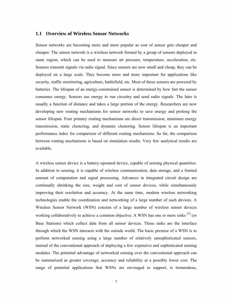
A five layer WSN model [2] is proposed based on these assumptions. The figure below shows
a generic WSN deployment and how individual layers of the model map to the underlying
WSN components.
Figure 1-1 Model for deployment of sensors in a Wireless Sensor Network
The sensors are deployed uniformly at random over the area of interest; once deployed, they
self-organize into a network that is expected to work unattended. The network is divided into
addressable regions. Each region contains a set of sensor nodes. An example of such an

6
organization can be provided using a base station (sink) that serves as a center of a polar
coordinate system. The distance between a sensor and the sink is determined based on the
(quantified) base-station signal level, as measured by the sensor node. The (quantified) angle
between a sensor and the sink (relative to a reference direction) is determined by directional
transmission from the sink. As a result, the area covered with sensors is divided into regions.
Each region is uniquely identified by its distance from the sink (an integer) and its angle (an
integer). All sensors within the region have the same values for distance and angle. The
mission determines the overall functioning of the WSN. It describes a high-level goal of the
WSN, i.e. what data is of interest and what types of services are needed. A set of services is
provided in support of a given mission. A service includes data collection and processing
from large areas of the WSN. Since individual sensors are identified only by their region,
service-related activities within a region are considered to be atomic. The service can be
decomposed into a set of services, each limited to a single region and involving all the active
sensors in the region. The sender, requesting such service, may be in the same region or
outside the region. Requesting, performing and replying to the service necessitate
communication among sensors. Each sensor has a set of sensory/control capabilities,
described by attributes with a specified range of values and a specified resolution.
Importantly, a given mission only requires a subset of capabilities, referred to as the sensor
configuration. Thus, the configuration of individual sensors is determined by the mission of
the WSN. A change in the mission often requires a change in the sensor configuration.
1.3 Challenges
Previously, sensor networks consisted of small number of sensor nodes that were wired to a
central processing station. However, nowadays, the focus is more on wireless, distributed,
sensing nodes. But, why distributed, wireless sensing? When the exact location of a particular
phenomenon is unknown, distributed sensing allows for closer placement to the phenomenon
than a single sensor would permit. Also, in many cases, multiple sensor nodes are required to
overcome environmental obstacles like obstructions, line of sight constraints etc. In most
cases, the environment to be monitored does not have an existing infrastructure for either
energy or communication. It becomes imperative for sensor nodes to survive on small, finite
sources of energy and communicate through a wireless communication channel.
The information gathering capabilities of distributed sensor networks are poised to
revolutionize the way the information infrastructure interacts with our physical environment.

7
Projecting IC cost curves into the future leads us to conclude that wireless sensing systems on
a chip will soon become so low-cost that that wireless capabilities will be built into
everything, from your home garden to stuffed animals to library books.
If wireless sensors are to become pervasive in businesses and homes, researchers must
provide inexpensive ICs. Due to the large densities of nodes, networks must be zero-
configuration, and zero-maintenance. In addition, the very long life required for autonomous
operation dictates that these devices must be extremely energy efficient for their energy
sources to last for the full life of the product to which they are attached.
In the majority of applications, locating sensors is also critical. An alarm from a sensor may
be meaningless unless the source is identified and located. If devices are to be dropped into
place or moved periodically users should not be required to input each device ID and its
coordinates, nor should the user interface identify devices by number. In fact, a device's
location can become its ID. Location of a device will be relative to its neighbours, which it
will cooperatively calculate based on peer-to-peer range measurements. Furthermore, sensor
data fusion and processing algorithms will reduce and make decisions based on the relative
location of input data.
Another requirement for sensor networks would be distributed processing capability. This is
necessary since communication is a major consumer of energy. A centralized system would
mean that some of the sensors would need to communicate over long distances that lead to
even more energy depletion. Hence, it would be a good idea to process locally as much
information as possible in order to minimize the total amount of information to be
transmitted.
1.4 Objective of the Project
The scope of the project involves the design and fabrication of a Base Station board and a
Remote Sensor Node board. The key objective is to establish a wireless link between the
Base Station and the Remote Sensor Node. Over the wireless link data from the sensors
housed on the Remote Sensor Node is to be transmitted to the Base Station. Received data at
the Base Station must then be processed and displayed the computer terminal. The computer
terminal is equipped with the software designed exclusively for the project using c#. c# is the
programming language from the package Visual Studio, it works in very similar way as of

8
usual c or c++. For the interfacing of the device with PC terminal, we have used USB ports,
which is a revolutionary step towards data communication with Atmel Microcontrollers
especially without USB interfacing facilities. There may be one or more different sensors for
various measureable physical quantities. Under this project, temperature sensing is the prime
focus. Wireless communication is required to occur at 2.4 GHz which is an industrial
standard and is extensively used in Bluetooth, ZigBee and similar wireless communication
technologies. This would facilitate easy transition into commercial applications.
As far as the data communication is concerned, the packet transfer between the Base Station
and the Remote Sensor Node should be efficient. Unnecessary overheads must be eliminated
while all the required data must be transmitted and received without errors. Packets generated
for transmission should include identity of the Remote Sensor Node, data to be recorded and
provision for error control.
The chief aim of the project is to achieve reduction in power consumption at the Remote
Sensor Node and if possible the Base Station too. This should be achieved without loss in
reliability and sensitivity. Components should be chosen to suit this objective. The circuits
have been designed with accurately manipulated components, most of which have SMD
(Surface Mounting Device) packages. The PCBs are also made as small as possible to reduce
power consumption and increase reliability. They also posses the specialities in terms of PTH
(Plated Through Hole) technology. The optimization of the circuit is the main purpose of the
design.

9
2 PRIOR STUDIES

10
2.1 Cross-bow sensor network kit Cross-bow has developed a specialized study kit for domestic purpose to study and simulate
the sensor network. It shows the practical demonstration of a network with several sensors
like temperature, light, and voice. The study of this kit helps understanding the sensor
network. The design also inspires to make the actual hardware related to the project. [4]
The applications for Wireless Sensor Networks are almost limitless with industries and
deployments having specific technology requirements such as reliability, battery-life, range,
frequencies, topologies, size of the network, sampling rate and sensor use.
To address the unique requirements of individual applications, Crossbow provides a broad
portfolio of wireless sensor network products that allow you to choose the optimal solution
for your industry, application and geographical requirements.
Development Kits
They provide users with a pre-configured set of hardware to get started with Crossbow’s Mote
hardware. Whether you are just getting started with Crossbow’s hardware, or looking to create
your own OEM hardware, or need a packaged system for outdoor deployments – there is a kit
for you.
Wireless Modules
These are available in many different forms. Depending on the radio frequency and platform
requirements you may have for your application, there is a variety of wireless modules to
choose from whether it is our popular IRIS or TelosBMote to our high-power Imote2 device.
Sensor Boards
They set Crossbow apart from other wireless sensor network platform providers. Our large
offering ranges from light, temp and humidity to GPS, magnetometers and barometric
pressure. Coupled with our versatile data acquisition boards that allow users to interface their
own sensors, it is easy to see why Crossbow is the chosen company for any wireless sensor
application.
Gateways
11
They provide users with real-time access to their data. Simple USB and serial interface boards
are available as well as the Stargaze Net bridge which is a full-fledged embedded sensor
network gateway.
2.1.1 Robust Mesh Network Traditional wireless RS485 often uses fixed routing, therefore any radio path is a critical path.
The proprietary Xmesh radio protocol is a self-forming / self-healing wireless mesh network
with ad-hoc multi-hopping capabilities. Therefore if any path becomes unreliable, the
network will automatically find a new, better path to stay in reliable multi-point
communications. MEMSIC/Crossbow-Japan, being a pioneer in wireless mesh networks, has
proven the robustness of Xmesh through deployments of wireless energy systems in energy,
storage, factory maintenance, and other various applications, of which over 30,000 nodes are
steadily working today. The WS-Z5000A uses IEEE802.15.4 standard, 2.4GHz radio.
The WS-Z5000A has numerous intuitive features that facilitate the ease in installation.
- RS485 line connection is easy to install by simply inserting lines into the push-in terminals.
- Packet communications to/from the equipment and to/from another node are indicated by
LEDs.
- Node ID, Group ID, and radio channel are selectable by switch, enabling these parameters.
- Mounting can be done by screws, hooks, or magnets.
2.2 Arduino [5] Arduino is an open hardware concept, developed by the students of university of Italy.
Arduino is an open-source physical computing platform based on a simple I/O board and a
development environment that implements the Processing/Wiring language. Arduino can be
used to develop stand-alone interactive objects or can be connected to software on your
computer (e.g. Flash, Processing, and MaxMSP). The boards can be assembled by hand or
purchased preassembled; the open-source
IDE can be downloaded for free.

12
2.2.1 Features An Arduino is a single-board microcontroller and a software suite for programming it. The
hardware consists of a simple open hardware design for the controller with an Atmel
AVR processor and on-board I/O support. The software consists of a standard programming
language and the boot loader that runs on the board
Hardware
An Arduino board consists of an 8-bit Atmel AVR microcontroller with complementary
components to facilitate programming and incorporation into other circuits. An important
aspect of the Arduino is the standard way that connectors are exposed allowing the CPU
board to be connected to a variety of interchangeable add-on modules (known as shields).
Official Arduinos have used the megaAVR series of chips, specifically the ATmega8. At a
conceptual level, when using the Arduino software stack all boards are programmed over
an RS-232 serial connection, but the way this is implemented in hardware varies by version.
Serial Arduino boards contain a simple inverter circuit to convert between RS-232-level
and TTL-level signals. Current Arduino boards are programmed via USB, implemented using
USB-to-serial adapter chips such as the FTDI FT232.
2.2.2 Software
The Arduino IDE is a cross-platform application written in Java which is derived from the
IDE made for the Processing programming language and the Wiring project. It includes a
code editor with features such as syntax highlighting, brace matching, and automatic
indentation, and is also capable of compiling and uploading programs to the board with a
single click. There is typically no need to edit Make files or run programs on the command.
The Arduino IDE comes with a C/C++ library called "Wiring" (from the project of the same
name), which makes many common input/output operations much easier. Arduino programs
are written in C/C++, although users only need to define two functions in order to make a
runnable program:
setup() – a function run once at the start of a program which can be used for
initializing settings, and
loop() – a function called repeatedly until the board is powered off.

13
2.2.3 Overview of the hardware used for study
The Arduino Duemilanove ("2009") is a microcontroller board based on the ATmega168. It
has 14 digital input/output pins (of which 6 can be used as PWM outputs), 6 analog inputs, a
16 MHz crystal oscillator, a USB connection, a power jack, an ICSP header, and a reset
button. It contains everything needed to support the microcontroller; simply connect it to a
computer with a USB cable or power it with a AC-to-DC adapter or battery to get started.
"Duemilanove" means 2009 in Italian and is named after the year of its release. The
Duemilanove is the latest in a series of USB Arduino boards; for a comparison with previous
versions, see the index of Arduino boards.
Table 1 Summary of Arduino hardware
Microcontroller ATmega168
Input Voltage 6-20V
Digital I/O Pins 14 (of which 6 provide PWM output)
Analog Input Pins 6
Flash Memory 16 KB (ATmega168) of which 2 KB used by bootloader
SRAM 1 KB (ATmega168)
EEPROM 512 bytes (ATmega168)
Clock Speed 16 MHz
Software
The open-source Arduino environment makes it easy to write code and upload it to the i/o
board. It runs on Windows, Mac OS X, and Linux. The environment is written in Java and
based on Processing, avr-gcc, and other open source software.
Programming using Processing language
Processing is an open source "programming language and integrated development
environment (IDE) built for the electronic arts and visual design communities" with the
purpose of teaching the basics of computer programming in a visual context, and to serve as
the foundation for electronic sketchbooks. The project was initiated in 2001 by Casey

14
Reas and Ben Fry, both formerly of the Aesthetics and Computation Group at the MIT Media
Lab.
2.2.4 Bootloader [6] A boot sequence is the initial set of operations that the computer performs when power is
switched on. The bootloader typically loads the main operating system for the computer.
A computer's central processor can only execute program code found in Read-Only Memory
(ROM) and Random Access Memory (RAM). Modern operating systems and application
program code and data are stored on non-volatile data storage devices, such as hard disk
drives, CD, DVD, USB flash drive, and floppy disk. When a computer is first powered on, it
does not have an operating system in ROM or RAM. The computer must initially execute a
small program stored in ROM along with the bare minimum of data needed to access the non-
volatile devices from which the operating system programs and data are loaded into RAM.
The small program that starts this sequence of loading into RAM, is known as a bootstrap
loader, bootstrap or boot loader. This small boot loader program's only job is to load other
data and programs which are then executed from RAM. Often, multiple-stage boot loaders
are used, during which several programs of increasing complexity sequentially load one after
the other in a process of chain loading.
When you upload a sketch, you're using the Arduino bootloader, a small program that has
been loaded on to the microcontroller on your board. It allows you to upload code without
using any additional hardware. The bootloader is active for a few seconds when the board
resets; then it starts whichever sketch was most recently uploaded to the microcontroller.

15
3 HARDWARE DESCRIPTION

16
Multipurpose Wireless Transceiver Node
Figure 3-1 Wireless Sensor Node Component Layout
Power Supply: Jumper Settings: Via USB As a Base Station: POW JMP connector Remove TXD, RXD Jumper Insert DIN – DOUT Left side Status LEDs: TX – Transmit Status As a Stand Alone Node: RX – Receive Status Insert TXD, RXD Jumper L1 – Power ON Insert DIN – DOUT Right Side L2 – XBEE Status L4 – Reset

17
3.1 Hardware Requirements
The basic requirement of the various components used in the circuits involved in the project
is that they must operate at low power levels. Especially, the microcontroller and the Radio
Frequency (RF) communication ICs should be chosen with great care as these components
contribute most to power consumption and dissipation.
Further it is necessary that the Printed Circuit Boards (PCBs) that are to house various circuit
components should be designed meticulously taking into consideration the main aim of the
project. Placement of components, routing of tracks for connecting the components, thickness
of the routing tracks etc. should be paid careful attention to so that dissipation of power may
be reduced to the greatest extent.
Since the chosen frequency of operation is 2.4 GHz, the design of the RF section on the PCB
must be carried out with appropriate considerations for noise reduction and optimum
coupling of power.
The main area of application of the project is in Wireless Sensor Networks. In such wireless
networks, size of sensor nodes is required to be minimal so as to facilitate deployment in any
possible environment. This necessitates that the PCBs be designed as small as possible
without compromising on performance, capability and functions.
3.2 Block Diagram
3.2.1 Base Station The Base Station (BS) is responsible for receiving data from the sensor nodes and processing
it as required. The microcontroller forms the heart of the BS and is responsible for enabling
wireless communication, data packet formation, data packet decoding, data forwarding and
displaying the received values on the on-board LCD. The microcontroller is connected to the
RF communication unit which consists of the RF integrated circuit and antenna. The
microcontroller is interfaced with the XBee module using SPI.

18
Figure 3-2 Block Diagram for Base Station
The microcontroller is also interfaced with a computer terminal using the USB interfaces.
This is meant to forward the received data to the computer terminal for displaying it on a GUI
and further processing, decision making etc. as may be necessary. All the components in the
BS are powered by a Power Unit. It consists of a battery or power supply (whichever is
available) and voltage regulators which limit the voltage to certain values in order to protect
the components and to reduce unnecessary power consumption.
3.2.2 Remote Sensor Node
The design of the Remote Sensor Node (SN) is a very crucial part of the project. In
construction it is similar to the BS. The SN consists of a microcontroller which collects
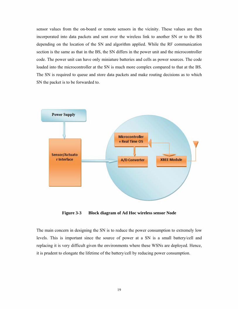
19
sensor values from the on-board or remote sensors in the vicinity. These values are then
incorporated into data packets and sent over the wireless link to another SN or to the BS
depending on the location of the SN and algorithm applied. While the RF communication
section is the same as that in the BS, the SN differs in the power unit and the microcontroller
code. The power unit can have only miniature batteries and cells as power sources. The code
loaded into the microcontroller at the SN is much more complex compared to that at the BS.
The SN is required to queue and store data packets and make routing decisions as to which
SN the packet is to be forwarded to.
Figure 3-3 Block diagram of Ad Hoc wireless sensor Node
The main concern in designing the SN is to reduce the power consumption to extremely low
levels. This is important since the source of power at a SN is a small battery/cell and
replacing it is very difficult given the environments where these WSNs are deployed. Hence,
it is prudent to elongate the lifetime of the battery/cell by reducing power consumption.

20
3.3 Hardware Components
3.3.1 XBee RF Module [7]
Figure 3-4 XBEE Module
The XBee and XBee-PRO OEM RF Modules were engineered to meet IEEE 802.15.4
standards and support the unique needs of low-cost, low-power wireless sensor networks. The
modules require minimal power and provide reliable delivery of data between devices. The
modules operate within the ISM 2.4 GHz frequency band and are pin-for-pin compatible with
each other.
XBee multipoint RF modules are ideal for applications requiring low latency and predictable
communication timing. Providing quick, robust communication in point-to-point, peer-to-
peer, and multipoint/star configurations, XBee multipoint products enable robust end-point
connectivity with ease. Whether deployed as a pure cable replacement for simple serial
communication, or as part of a more complex hub-and-spoke network of sensors, XBee
multipoint RF modules maximize wireless performance and ease of development.

21
Key Features
Long Range Data Integrity
Indoor/Urban: up to 100’ (30 m)
Outdoor line-of-sight: up to 300’ (100 m)
Transmit Power: 1 mW (0 dBm)
Receiver Sensitivity: -92 dBm
Low Power
TX Current: 45 mA (@3.3 V)
RX Current: 50 mA (@3.3 V)
Power-down Current: < 10 μA
Miscellaneous Features
802.15.4/Multipoint network topologies
2.4 GHz for worldwide deployment
900 MHz for long-range deployment
Fully interoperable Digi Drop-in Networking products, including gateways & device
Common XBee footprint for a variety of RF modules
Low-power sleep modes
Multiple antenna options
Industrial temperature rating (-40º C to 85º C)
Low power and long range variants available
Usability
A/D Conversion
Digital I/O lines
DSSS Support
No configuration necessary for out-of box RF communications
Free X-CTU Software
Extensive command set
Point-to-point, point-to-multipoint and peer-to-peer topologies supported
World Wide Acceptance
ISM (Industrial, Scientific & Medical) 2.4 GHz frequency band

22
RF Module Operation (Serial Communications) UART Data Flow
Serial Data Devices that have a UART interface can connect directly to the pins of the RF
module. System Data Flow Diagram in a UART‐interfaced environment (Low‐asserted
signals distinguished with horizontal line over signal name.) The XBee OEM RF Modules
interface to a host device through a logic-level asynchronous serial port. Through its serial
port, the module can communicate with any logic and voltage compatible UART; or through
a level translator to any serial device (For example: Through a Max- Stream proprietary RS-
232 or USB interface board).
API Operation
API (Application Programming Interface) Operation is an alternative to the default
Transparent Operation. The frame-based API extends the level to which a host application
can interact with the networking capabilities of the module. When in API mode, all data
entering and leaving the module is contained in frames that define operations or events within
the module.
Transmit Data Frames (received through the DI pin (pin 3)) include:
RF Transmit Data Frame
Command Frame (equivalent to AT commands)
Receive Data Frames (sent out the DO pin (pin 2)) include:
RF-received data frame
Command response
Figure 3.5 Voltage Level for UART
23
Event notifications such as reset, associate, disassociate, etc.
The API provides alternative means of configuring modules and routing data at the host
application layer. A host application can send data frames to the module that contain address
and payload information instead of using command mode to modify addresses. The module
will send data frames to the application containing status packets; as well as source, RSSI and
payload information from received data packets.
DI (Data In) Buffer
When serial data enters the RF module through the DI pin (pin 3), the data is stored in the DI
Buffer until it can be processed. Hardware Flow Control (CTS). When the DI buffer is 17
bytes away from being full; by default, the module de-asserts CTS (high) to signal to the host
device to stop sending data [refer to D7 (DIO7 Configuration) parameter]. CTS is re-asserted
after the DI Buffer has 34 bytes of memory available.
DO (Data Out) Buffer
When RF data is received, the data enters the DO buffer and is sent out the serial port to a
host device. Once the DO Buffer reaches capacity, any additional incoming RF data is lost.
Hardware Flow Control (RTS). If RTS is enabled for flow control (D6 (DIO6 Configuration)
Parameter = 1), data will not be sent out the DO Buffer as long as RTS (pin 16) is de-
asserted.
XBee Addressing Modes
Every RF data packet sent over-the-air contains a Source Address and Destination Address
field in its header. The RF module conforms to the 802.15.4 specification and supports both
short 16-bit addresses and long 64-bit addresses, To send a packet to a specific module using
64-bit addressing: Set Destination Address (DL + DH) to match the Source Address (SL +
SH) of the intended destination module. To send a packet to a specific module using 16-bit
addressing: Set DL (Destination Address Low) parameter to equal the MY parameter and set
the DH (Destination Address High) parameter to ‘0’.
24
Unicast Mode
By default, the RF module operates in unicast Mode. Unicast Mode is the only mode that
supports retries. While in this mode, receiving modules send an ACK (acknowledgement) of
RF packet reception to the transmitter. If the transmitting module does not receive the ACK,
it will re-send the packet up to three times or until the ACK is received.
Short 16-bit addresses. The module can be configured to use short 16-bit addresses as the
Source Address by setting (MY < 0xFFFE). Setting the DH parameter (DH = 0) will
configure the Destination Address to be a short 16-bit address (if DL < 0xFFFE). For two
modules to communicate using short addressing, the Destination Address of the transmitter
module must match the MY parameter of the receiver.
Long 64-bit addresses. The RF module’s serial number (SL parameter concatenated to the
SH parameter) can be used as a 64-bit source address when the MY (16-bit Source Address)
parameter is disabled. When the MY parameter is disabled (set MY = 0xFFFF or 0xFFFE),
the module’s source address is set to the 64-bit IEEE address stored in the SH and SL
parameters.
Broadcast Mode
Any RF module within range will accept a packet that contains a broadcast address. When
configured to operate in Broadcast Mode, receiving modules do not send ACKs
(Acknowledgements) and transmitting modules do not automatically re-send packets as is the
case in Unicast Mode. To send a broadcast packet to all modules regardless of 16-bit or 64-
bit addressing, set the desti-nation addresses of all the modules as shown below.
DL (Destination Low Address) = 0x0000FFFF
DH (Destination High Address) = 0x00000000 (default value)
25
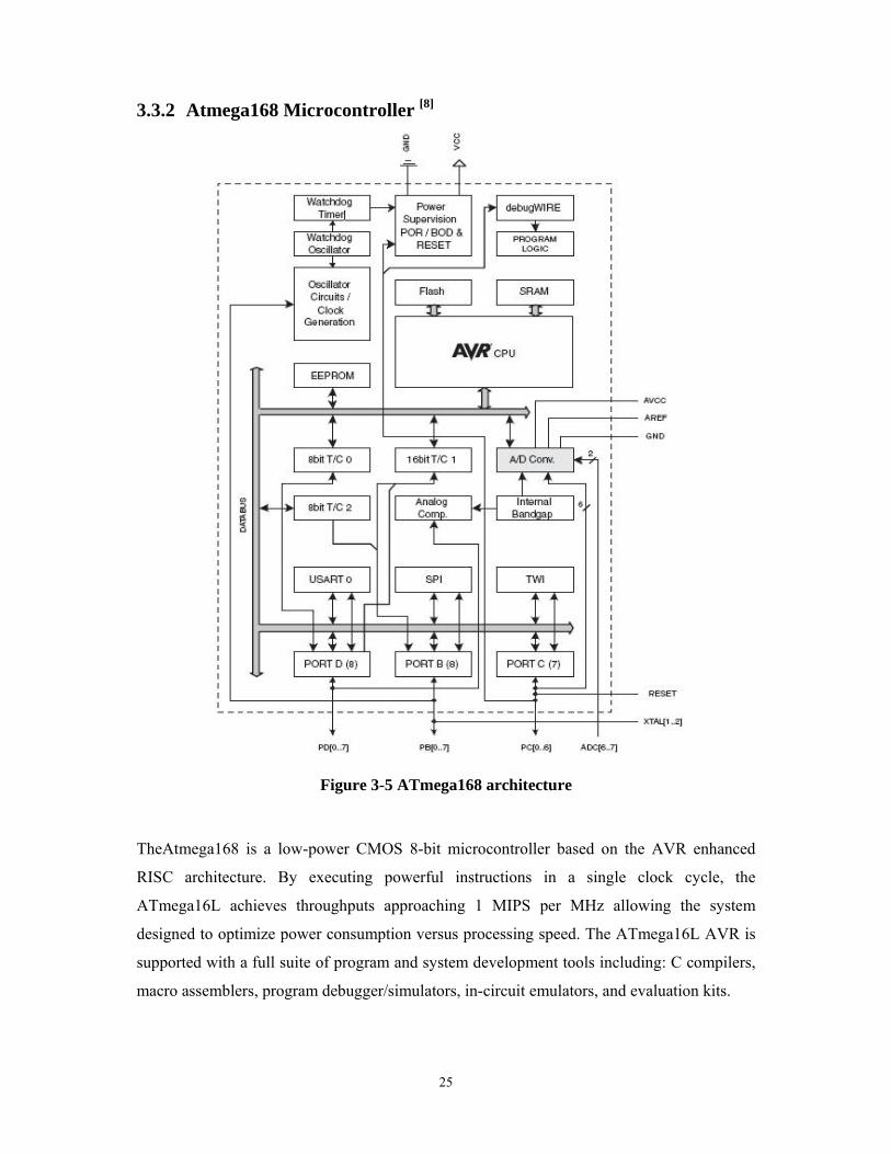
3.3.2 Atmega168 Microcontroller [8]
Figure 3-5 ATmega168 architecture
TheAtmega168 is a low-power CMOS 8-bit microcontroller based on the AVR enhanced
RISC architecture. By executing powerful instructions in a single clock cycle, the
ATmega16L achieves throughputs approaching 1 MIPS per MHz allowing the system
designed to optimize power consumption versus processing speed. The ATmega16L AVR is
supported with a full suite of program and system development tools including: C compilers,
macro assemblers, program debugger/simulators, in-circuit emulators, and evaluation kits.

26
The following features drive the choice of Atmega168 over other available microcontrollers:
• High-performance, Low-power AVR 8-bit Microcontroller
• Advanced RISC Architecture
o 131 Powerful Instructions – Most Single Clock Cycle Execution
o 32 x 8 General Purpose Working Registers
o Fully Static Operation
o Up to 20 MIPS Throughput at 20 MHz
o On-chip 2-cycle Multiplier
• High Endurance Non-volatile Memory Segments
o 16K Bytes of In-System Self-Programmable Flash program memory
o 512 Bytes EEPROM
o 1K Bytes Internal SRAM
o Write/Erase Cycles: 10,000 Flash/100,000 EEPROM
Peripheral Features
o Two 8-bit Timer/Counters with Separate Prescaler and Compare Mode
o One 16-bit Timer/Counter with Separate Prescaler, Compare & Capture Mode
o Real Time Counter with Separate Oscillator
o Six PWM Channels
o 8-channel 10-bit ADC in TQFP and QFN/MLF package
o Temperature Measurement
o 6-channel 10-bit ADC in PDIP Package
o Programmable Serial USART
o Master/Slave SPI Serial Interface
Special Microcontroller Features
o Power-on Reset and Programmable Brown-out Detection
o Internal Calibrated Oscillator
o External and Internal Interrupt Sources
o Six Sleep Modes: Idle, ADC Noise Reduction, Power-save, Power-down, Standby
and Extended Standby
o 23 Programmable I/O Lines

27
o Operating Voltage: 1.8 - 5.5V
o Speed Grade: 0 - 20 MHz @ 1.8 - 5.5V
o Low Power Consumption at 1
– Active Mode: 0.2 mA
– Power-down Mode: 0.1 μA
– Power-save Mode: 0.75 μA (Including 32 kHz RTC)
3.3.3 FT232R USB - UART Bridge Converter IC [9]
Figure 3-6 Diagram of FT232R IC
The FT232R is a USB to serial UART interface with the following advanced features
Single chip USB to asynchronous serial data transfer interface.
Entire USB protocol handled on the chip. No USB specific firmware programming
required.

28
Fully integrated 1024 bit EEPROM storing device descriptors and CBUS I/O
configuration.
Fully integrated USB termination resistors.
Fully integrated clock generation with no external crystal required plus optional clock
output selection enabling a glue-less interface to external MCU or FPGA.
Data transfer rates from 300 baud to 3 M baud (RS422, RS485 and RS232) at TTL
levels.
256 byte receive buffer and 128 byte transmit buffer utilising buffer smoothing
technology to allow for high data throughput.
Configurable CBUS I/O pins.
Transmit and receive LED drive signals. FIFO receive and transmit buffers for high
data throughput.
Synchronous and asynchronous bit bang interface options
Low USB bandwidth consumption.
USB 2.0 Full Speed compatible.
Low Power Consumption
+3.3V to +5.25V Single Supply Operation.
Integrated +3.3V level converter for USB I/O.
Integrated level converter on UART and CBUS for interfacing to between +1.8V and
+5V logic.
True 5V/3.3V/2.8V/1.8V CMOS drive output and TTL input. Low operating and
USB suspend current.
Typical Applications
USB to RS232/RS422/RS485 Converters
Upgrading Legacy Peripherals to USB
Cellular and Cordless Phone USB data transfer cables and interfaces
Interfacing MCU/PLD/FPGA based designs to USB
USB Audio and Low Bandwidth Video data transfer
PDA to USB data transfer
USB Smart Card Readers
USB Instrumentation
USB Industrial Control

29
USB MP3 Player Interface
USB FLASH Card Reader and Writers
Set Top Box PC - USB interface
USB Digital Camera Interface
USB Hardware Modems
USB Wireless Modems
USB Bar Code Readers
USB Software
3.4 Miscellaneous Hardware Parts: The hardware design is optimized for the components placement and power consumption.
For that purpose, the best choice of components is to use SMD (Surface Mounting Device)
components. Here is the list of the components used in the project circuit.
IC-XXXX - SOT223 Packaged SMD Voltage Regulator
Mini USB-B – SMD USB connector
c1206 – SMD Capacitors
r1206 – SMD Resistors
SMD LEDs (Red, Green)
Crystal Oscillator
Push Button switch for Reset
Male connectors for external connections to other devices such as sensors.
3.5 Protocols
3.5.1 ZigBee (IEEE 802.15.4) ZigBee is a specification for a suite of high level communication protocols using small, low-
power digital radios based on the IEEE 802.15.4-2003standard for wireless personal area
networks (WPANs), such as wireless headphones connecting with cell phones via short-range
radio. The technology defined by the ZigBee specification is intended to be simpler and less
expensive than other WPANs, such as Bluetooth. ZigBee is targeted at radio-frequency (RF)
applications that require a low data rate, long battery life, and secure networking.

30
ZigBee is a low-cost, low-power, wireless mesh networking proprietary standard. The low
cost allows the technology to be widely deployed in wireless control and monitoring
applications, the low power-usage allows longer life with smaller batteries.
Figure 3-7 Protocol Stack of ZigBee
Protocols:
The protocols build on recent algorithmic research (Ad-hoc On-demand Distance
Vector, neuRFon) to automatically construct a low-speed ad-hoc network of nodes. In most
large network instances, the network will be a cluster of clusters. It can also form a mesh or a
single cluster. The current profiles derived from the ZigBee protocols support beacon and
non-beacon enabled networks.
In non-beacon-enabled networks, an unslotted CSMA/CA channel access mechanism is used.
In this type of network, ZigBee Routers typically have their receivers continuously active,
requiring a more robust power supply. However, this allows for heterogeneous networks in
which some devices receive continuously, while others only transmit when an external
stimulus is detected. The typical example of a heterogeneous network is a wireless light
31
switch: The ZigBee node at the lamp may receive constantly, since it is connected to the
mains supply, while a battery-powered light switch would remain asleep until the switch is
thrown. The switch then wakes up, sends a command to the lamp, receives an
acknowledgment, and returns to sleep. In such a network the lamp node will be at least a
ZigBee Router, if not the ZigBee Coordinator; the switch node is typically a ZigBee End
Device.
In beacon-enabled networks, the special network nodes called ZigBee Routers transmit
periodic beacons to confirm their presence to other network nodes. Nodes may sleep between
beacons, thus lowering their duty cycle and extending their battery life. Beacon intervals may
range from 15.36 milliseconds to 15.36 ms * 214 = 251.65824 seconds at 250 Kbit/s, from 24
milliseconds to 24 ms * 214 = 393.216 seconds at 40 Kbit/s and from 48 milliseconds to 48
ms * 214 = 786.432 seconds at 20 Kbit/s. However, low duty cycle operation with long
beacon intervals requires precise timing, which can conflict with the need for low product
cost.
Device Types:
There are three different types of ZigBee [12] devices:
ZigBee coordinator (ZC): The most capable device, the coordinator forms the root of
the network tree and might bridge to other networks. There is exactly one ZigBee
coordinator in each network since it is the device that started the network originally.
ZigBee Router (ZR): As well as running an application function, a router can act as an
intermediate router, passing on data from other devices.
ZigBee End Device (ZED): Contains just enough functionality to talk to the parent
node (either the coordinator or a router); it cannot relay data from other devices. This
relationship allows the node to be asleep a significant amount of the time thereby
giving long battery life.
Typical Applications
Home Entertainment and Control — Smart lighting, advanced temperature control,
safety and security, movies and music

32
Home Awareness — Water sensors, power sensors, energy monitoring, smoke and fire
detectors, smart appliances and access sensors
Mobile Services — m-payment, m-monitoring and control, m-security and access
control, m-healthcare and tele-assist
Commercial Building — Energy monitoring, HVAC, lighting, access control
Industrial Plant — Process control, asset management, environmental management,
energy management, industrial device control
3.5.2 USB [13] Protocol USB (Universal Serial Bus) is a specification to establish communication between devices
and a host controller (usually personal computers), developed and invented by Intel. USB is
intended to replace many varieties of serial and parallel ports.
A USB system has an asymmetric design, consisting of a host, a multitude of downstream
USB ports, and multiple peripheral devices connected in a tiered-star topology.
Additional USB hubs may be included in the tiers, allowing branching into a tree structure
with up to five tier levels. A USB host may have multiple host controllers and each host
controller may provide one or more USB ports. Up to 127 devices, including hub devices if
present, may be connected to a single host controller
.

33
4 PRINTED CIRCUIT BOARD DESIGN

34
4.1 Introduction to PCB Design using Eagle 5.7.0
Eagle Layout Editor is a tool for designing PCB layout. Apart from designing, it also
provides various built-in features for design verification and manufacturing processing.
OrCAD capture provides a component information system that allows one to identify, utilize
and design with preferred parts. In the following subsection, a detailed description of the
features provided by OrCAD capture and OrCAD layout are discussed.
4.2 Features of Eagle 5.7.0
The EAGLE Layout Editor is an easy to use, yet powerful tool for designing printed circuit
boards (PCBs). The name EAGLE is an acronym, which stands for
Easily Applicable Graphical Layout Editor
• Maximum drawing area 1.6 x 1.6m (64 x 64 inch)
• Resolution 1/10,000mm (0.1 micron)
• Up to 16 signal layers
• Conventional and SMT parts
• Comes with a full set of part libraries
• Easy to create own parts with the fully integrated library editor
• Undo/redo function for ANY editing command, to any depth
• Script files for batch command execution
• Copper pouring
• Cut and paste function for copying entire sections of a drawing
• Design rule check
• Interactive Follow-me Router (requires the Autorouter module)
35
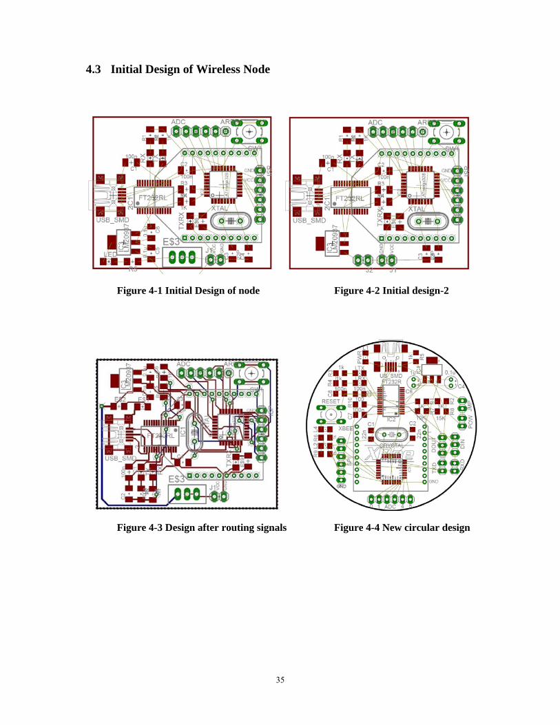
4.3 Initial Design of Wireless Node
Figure 4-1 Initial Design of node Figure 4-2 Initial design-2
Figure 4-3 Design after routing signals Figure 4-4 New circular design
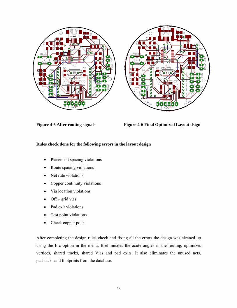
36
Figure 4-5 After routing signals Figure 4-6 Final Optimized Layout dsign
Rules check done for the following errors in the layout design
• Placement spacing violations
• Route spacing violations
• Net rule violations
• Copper continuity violations
• Via location violations
• Off – grid vias
• Pad exit violations
• Test point violations
• Check copper pour
After completing the design rules check and fixing all the errors the design was cleaned up
using the Erc option in the menu. It eliminates the acute angles in the routing, optimizes
vertices, shared tracks, shared Vias and pad exits. It also eliminates the unused nets,
padstacks and footprints from the database.
37
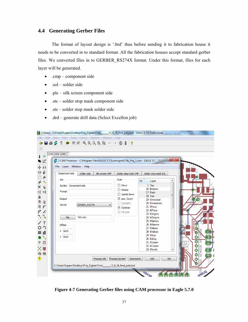
4.4 Generating Gerber Files
The format of layout design is ‘.brd’ thus before sending it to fabrication house it
needs to be converted in to standard format. All the fabrication houses accept standard gerber
files. We converted files in to GERBER_RS274X format. Under this format, files for each
layer will be generated.
• .cmp – component side
• .sol – solder side
• .plc – silk screen component side
• .stc – solder stop mask component side
• .sts – solder stop mask solder side
• .drd – generate drill data (Select Excellon job)
Figure 4-7 Generating Gerber files using CAM processor in Eagle 5.7.0
38
5 COMMUNICATION INTERFACE

39
5.1 Serial Communication and USB Interface using FT232R
Two main types of on-board communication occur in the project. Serial communication over
via USB is achieved by the use of FT232R IC. FT232R works as USB to Serial bridge
converter. Communication between XBEE and microcontroller is done via UART. As well
as UART is used to made communication between User terminal and wireless node.
The FT232R is a USB to serial UART bridge interface device which simplifies USB to serial
designs and reduces external component count by fully integrating an external EEPROM,
USB termination resistors and an integrated clock circuit which requires no external crystal,
into the device. It has been designed to operate efficiently with a USB host controller by
using as little as possible of the total USB bandwidth available.
Figure 5-1 Basic Connections of FTDI to controller
40
Signals Used in FT232R
• TXDEN# - transmit enable for RS485 designs.
• PWREN# - Power control for high power, bus powered designs.
• TXLED# - for pulsing an LED upon transmission of data.
• RXLED# - for pulsing an LED upon receiving data.
• TX&RXLED# - which will pulse an LED upon transmission OR reception of data.
• SLEEP# - indicates that the device going into USB suspend mode.
• CLK48 / CLK24 / CLK12 / CLK6 - 48MHz, 24MHz, 12MHz, and 6MHz clock
output signal options.
Internal EEPROM
The internal EEPROM in the FT232R is used to store USB Vendor ID (VID), Product ID
(PID), device serial number, product description string and various other USB configuration
descriptors. The internal EEPROM is also used to configure the CBUS pin functions.
USB Transceiver
The USB Transceiver Cell provides the USB 1.1 / USB 2.0 full-speed physical interface to
the USB cable. The output drivers provide +3.3V level slew rate control signalling, whilst a
differential input receiver and two single ended input receivers provide USB data in.
USB DPLL
The USB DPLL cell locks on to the incoming NRZI USB data and generates recovered clock
and data signals for the Serial Interface Engine (SIE) block.
Internal 12MHz Oscillator
The Internal 12MHz Oscillator cell generates a 12MHz reference clock. This provides an
input to the x4 Clock Multiplier function. The 12MHz Oscillator is also used as the reference
clock for the SIE, USB Protocol Engine and UART FIFO controller blocks.
Serial Interface Engine (SIE)
The Serial Interface Engine (SIE) block performs the parallel to serial and serial to parallel
conversion of the USB data. In accordance with the USB 2.0 specification, it performs bit
stuffing/un-stuffing. It checks CRC (Cyclic redundancy check) on the USB data-stream.

41
USB Protocol Engine
The USB Protocol Engine manages the data stream from the device USB control endpoint. It
handles the low level USB protocol requests generated by the USB host controller and the
commands for controlling the functional parameters of the UART in accordance with the
USB 2.0 specification.
FIFO TX Buffer (128 bytes)
Data from the USB data OUT endpoint is stored in the FIFO TX buffer and removed from
the buffer to the UART transmit register under control of the UART FIFO controller.
FIFO RX Buffer (256 bytes)
Data from the UART receive register is stored in the FIFO RX buffer prior to being removed
by the SIE on a USB data request from the device data IN endpoint.
UART FIFO Controller
The UART FIFO controller handles the transfer of data between the FIFO RX and TX
buffers and the UART transmit and receive registers.
5.2 Configuring FT232R
5.2.1 Driver Installation
To access FT232R on PC, FTDI USB drivers must be installed on PC. Once drivers
get installed, It can be detect using FT_PROG software (www.ftdichip.com).
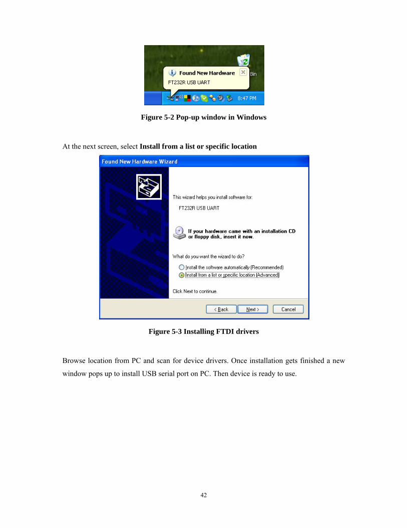
When you plug in the node, you may hear a sound from the computer and a little popup
bubble in the bottom right corner of the screen that says ‘Found New Hardware FT232R
USB UART’
42
Figure 5-2 Pop-up window in Windows
At the next screen, select Install from a list or specific location
Figure 5-3 Installing FTDI drivers
Browse location from PC and scan for device drivers. Once installation gets finished a new
window pops up to install USB serial port on PC. Then device is ready to use.
43
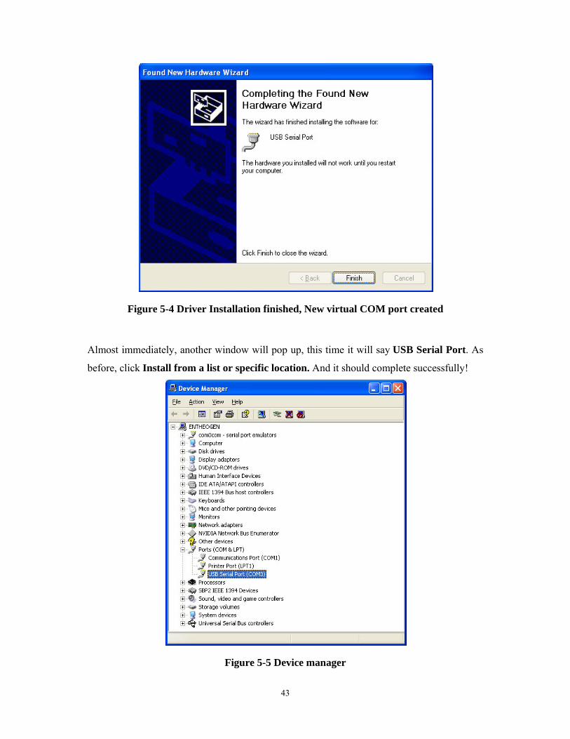
Figure 5-4 Driver Installation finished, New virtual COM port created
Almost immediately, another window will pop up, this time it will say USB Serial Port. As
before, click Install from a list or specific location. And it should complete successfully!
Figure 5-5 Device manager
44
When the computer is done rebooting, make sure the node is plugged in (and the red light is
lit). Go to the Device Manager (From the Start Menu, select Settings->Control Panel.
Double click on System and select the Hardware tab. Then click on the Device
Manager button)
Look for an entry under Ports (COM & LPT) that says USB Serial Port (COM) the COM
number may vary but it should be something like COM3 orCOM4. The COM stands for
"communication", and each one has a unique number, known as the COM Port number. In
this case the COM Port number is COM3.
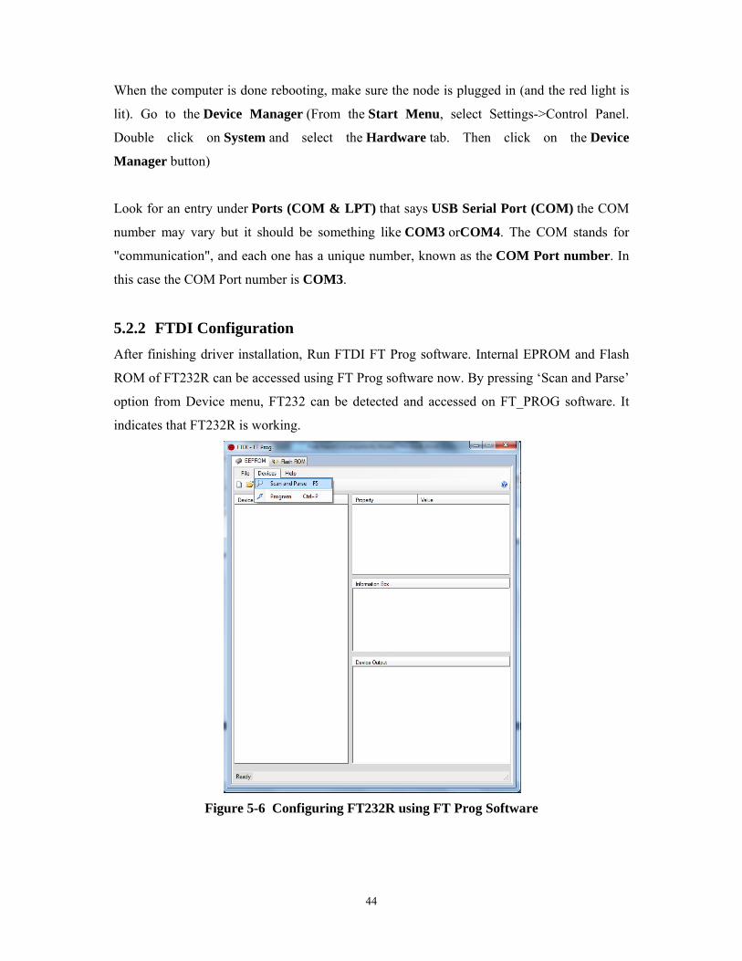
5.2.2 FTDI Configuration After finishing driver installation, Run FTDI FT Prog software. Internal EPROM and Flash
ROM of FT232R can be accessed using FT Prog software now. By pressing ‘Scan and Parse’
option from Device menu, FT232 can be detected and accessed on FT_PROG software. It
indicates that FT232R is working.
Figure 5-6 Configuring FT232R using FT Prog Software
45
5.3 Wireless Communication using IEEE 802.15.4 XBEE module
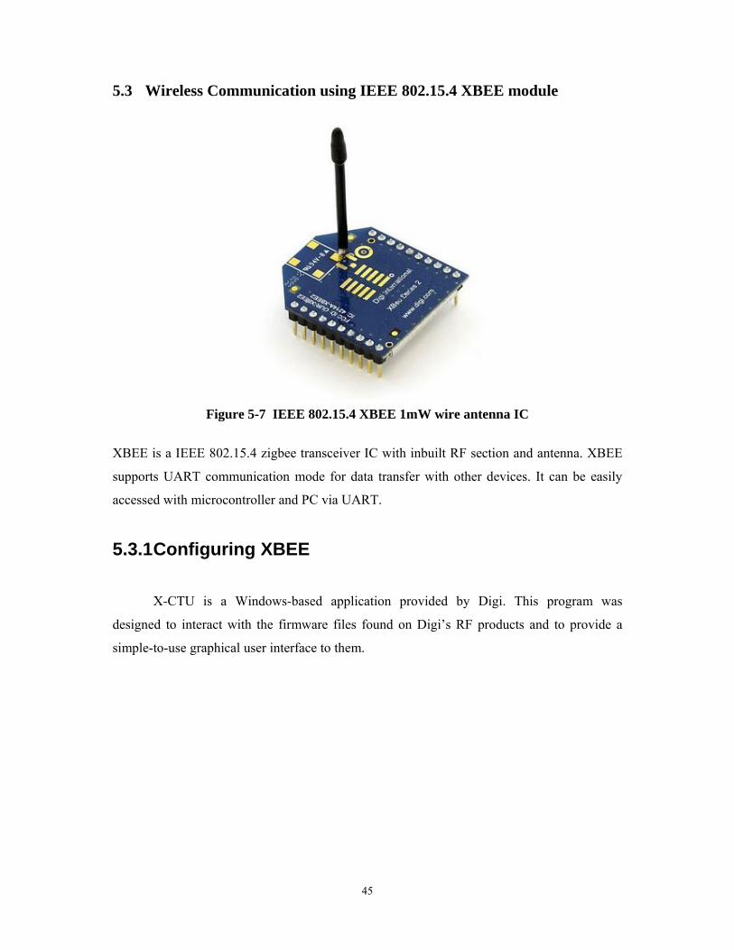
Figure 5-7 IEEE 802.15.4 XBEE 1mW wire antenna IC
XBEE is a IEEE 802.15.4 zigbee transceiver IC with inbuilt RF section and antenna. XBEE
supports UART communication mode for data transfer with other devices. It can be easily
accessed with microcontroller and PC via UART.
5.3.1 Configuring XBEE
X-CTU is a Windows-based application provided by Digi. This program was
designed to interact with the firmware files found on Digi’s RF products and to provide a
simple-to-use graphical user interface to them.

Figur
Figur
re 5-9 Mode
e 5-8 GUI o
em Configu
46
of X-CTU a
uration usin
application
g X-CTU ap
pplication

47
PC Settings
Allows user to select the desired COM port and configure that port to fit the radios settings.
Range Test
Allows user to perform a range test between two radios.
Terminal
Allows access to the computer’s COM port with a terminal emulation program. This tab also
allows the ability to access the radios’ firmware using AT commands.
Modem Configuration
Allows user to program the radios’ firmware settings via a graphical user interface. This tab
also allows customers the ability to change firmware version also. This operation is
performed via AT commands. Using AT commands following parameters can set..
• Channel ID
• Device ID
• Power mode
• Sleep mode settings
• Data rate
• TX – RX power level
• Parity check
• Security (Encryption key)
• I/O settings
• Firmware update
5.4 Universal Asynchronous Receiver Transmitter (UART) Interface
A Universal Asynchronous Receiver/Transmitter a computer hardware that translates data
between parallel and serial forms. UARTs are commonly used in conjunction with other
communication standards.
A UART is usually an individual (or part of an) integrated circuit used for serial
communications over a computer or peripheral device serial port. UARTs are now commonly
included in microcontrollers. Many modern ICs now come with a UART that can also

48
communicate synchronously (e.g. FT232R); these devices are called USARTs (universal
synchronous/asynchronous receiver/transmitter).
A UART usually contains the following components:
A clock generator, usually a multiple of the bit rate to allow sampling in the middle of a
bit period.
Input and output shift registers
Transmit/receive control
Read/write control logic
Transmit/receive buffers (optional)
Parallel data bus buffer (optional)
First-in, first-out (FIFO) buffer memory (optional)
5.4.1 Transmitting and receiving serial data
The Universal Asynchronous Receiver/Transmitter (UART) controller is the key component
of the serial communications subsystem of a computer. The UART takes bytes of data and
transmits the individual bits in a sequential fashion. At the destination, a second UART re-
assembles the bits into complete bytes. Serial transmission of digital information (bits)
through a single wire or other medium is much more cost effective than parallel transmission
through multiple wires. A UART is used to convert the transmitted information between its
sequential and parallel form at each end of the link. Each UART contains a shift
register which is the fundamental method of conversion between serial and parallel forms.
The UART usually does not directly generate or receive the external signals used between
different items of equipment. Typically, separate interface devices are used to convert the
logic level signals of the UART to and from the external signaling levels.
As of 2008, UARTs are commonly used with RS-232 for embedded systems
communications. It is useful to communicate between microcontrollers and also with PCs.
Many chips provide UART functionality in silicon, and low-cost chips exist to convert logic
level signals (such as TTL voltages) to RS-232 level signals (for example, FT232R, used in
the project)
49
5.4.2 Asynchronous receiving and transmitting
In asynchronous transmitting, teletype-style UARTs send a "start" bit, five to eight data bits,
least-significant-bit first, an optional "parity" bit, and then one, one and a half, or two "stop"
bits. The start bit is the opposite polarity of the data-line's idle state. The stop bit is the data-
line's idle state, and provides a delay before the next character can start. (This is called
asynchronous transmission). In mechanical teletypes, the "stop" bit was often stretched to two
bit times to give the mechanism more time to finish printing a character. A stretched "stop"
bit also helps resynchronization
Asynchronous transmission allows data to be transmitted without the sender having to send a
clock signal to the receiver. Instead, the sender and receiver must agree on timing parameters
in advance and special bits are added to each word which is used to synchronize the sending
and receiving units.
When a word is given to the UART for Asynchronous transmissions, a bit called the "Start
Bit" is added to the beginning of each word that is to be transmitted. The Start Bit is used to
alert the receiver that a word of data is about to be sent, and to force the clock in the receiver
into synchronization with the clock in the transmitter. These two clocks must be accurate
enough to not have the frequency drift by more than 10% during the transmission of the
remaining bits in the word.
After the Start Bit, the individual bits of the word of data are sent, with the Least Significant
Bit (LSB) being sent first. Each bit in the transmission is transmitted for exactly the same
amount of time as all of the other bits, and the receiver “looks” at the wire at approximately
halfway through the period assigned to each bit to determine if the bit is a 1 or a 0. For
example, if it takes two seconds to send each bit, the receiver will examine the signal to
determine if it is a 1 or a 0 after one second has passed, then it will wait two seconds and then
examine the value of the next bit, and so on.
Table Data Stream in Serial Communication
Start Data 0 Data 1 Data 2 Data 3 Data 4 Data 5 Data 6 Data 7 END
50
When the entire data word has been sent, the transmitter may add a Parity Bit that the
transmitter generates. The Parity Bit may be used by the receiver to perform simple error
checking. Then at least one Stop Bit is sent by the transmitter.
All operations of the UART hardware are controlled by a clock signal which runs at a
multiple (say, 16) of the data rate - each data bit is as long as 16 clock pulses. The receiver
tests the state of the incoming signal on each clock pulse, looking for the beginning of the
start bit. If the apparent start bit lasts at least one-half of the bit time, it is valid and signals the
start of a new character. If not, the spurious pulse is ignored. After waiting a further bit time,
the state of the line is again sampled and the resulting level clocked into a shift register. After
the required number of bit periods for the character length (5 to 8 bits, typically) have
elapsed, the contents of the shift register is made available (in parallel fashion) to the
receiving system. The UART will set a flag indicating new data is available, and may also
generate a processor interrupt to request that the host processor transfers the received data. In
some common types of UART, a small first-in, first-out (FIFO) buffer memory is inserted
between the receiver shift register and the host system interface. This allows the host
processor more time to handle an interrupt from the UART and prevents loss of received data
at high rates.
Transmitting and receiving UARTs must be set for the same bit speed, character length,
parity, and stop bits for proper operation. The receiving UART may detect some mismatched
settings and set a "framing error" flag bit for the host system; in exceptional cases the
receiving UART will produce an erratic stream of mutilated characters and transfer them to
the host system.
Typical serial ports used with personal computers connected to modems use eight data bits,
no parity, and one stop bit; for this configuration the number of ASCII character per seconds
equals the bit rate divided by 10
5.4.3 Special Receiver Condition
Overrun Error
An "overrun error" occurs when the USART receiver cannot process the character that just
came in before the next one arrives. Various USART devices have different amounts of
buffer space to hold received characters. The CPU must service the USART in order to

51
remove characters from the input buffer. If the CPU does not service the USART quickly
enough and the buffer becomes full, an Overrun Error will occur.
Under-run Error
An "under-run error" occurs when the UART transmitter has completed sending a character
and the transmit buffer is empty. In asynchronous modes this is treated as an indication that
no data remains to be transmitted, rather than an error, since additional stop bits can be
appended. This error indication is commonly found in USARTs, since an under-run is more
serious in synchronous systems.
Framing Error
A "framing error" occurs when the designated "start" and "stop" bits are not valid. As the
"start" bit is used to identify the beginning of an incoming character, it acts as a reference for
the remaining bits. If the data line is not in the expected idle state when the "stop" bit is
expected, a Framing Error will occur.
Parity Error
A "parity error" occurs when the number of "active" bits does not agree with the specified
parity configuration of the USART, producing a Parity Error. Because the "parity" bit is
optional, this error will not occur if parity has been disabled. Parity error is set when the
parity of an incoming data character does not match the expected value.
Break Condition
A "break condition" occurs when the receiver input is at the "space" level for longer than
some duration of time, typically, for more than a character time. This is not necessarily an
error, but appears to the receiver as a character of all zero bits with a framing error.
Some equipment will deliberately transmit the "break" level for longer than a character as an
out-of-band signal. When signalling rates are mismatched, no meaningful characters can be
sent, but a long "break" signal can be a useful way to get the attention of a mismatched
receiver to do something (such as resetting itself). Unix-like systems can use the long "break"
level as a request to change the signalling rate, to support dial-in access at multiple signalling
rates.

52
6 SOFTWARE INTERFACE
53
6.1 Compiler and Simulation Software
The Writing, compiling & debugging of the programming code is done by the use of
NetBeans. NetBeans refers to both a platform framework for Java desktop applications, and
an Integrated Development Environment (IDE) for developing with JAVA, C, C++,
Python and many other programming languages.
6.1.1 NetBeans IDE 6.8: [10]
The NetBeans IDE is an open source IDE, written in Java and runs everywhere where a JVM
(Java Virtual Machine) is installed, including Windows, Mac OS & Linux. A JDK (Java
Development Kit) is required for Java development functionality, but is not required for
development in other programming languages.
The NetBeans Platform allows applications to be developed from a set of modular software
components called modules. Applications based on the NetBeans platform (including the
NetBeans IDE) can be extended by us.
The platform offers reusable services common to desktop applications, allowing developers
to focus on the logic specific to their application. Among the features of the platform are:
User interface management (e.g. menus and toolbars)
User settings management
Storage management (saving and loading any kind of data)
Window management
Wizard framework (supports step-by-step dialogs)
NetBeans Visual Library
NetBeans Features:
These modules are part of the NetBeans IDE.
NetBeans Profiler
The NetBeans Profile is a tool for the monitoring of Java applications: It helps you find
memory leaks and optimize speed. Formerly downloaded separately, it is integrated into the
core IDE since version 6.0.
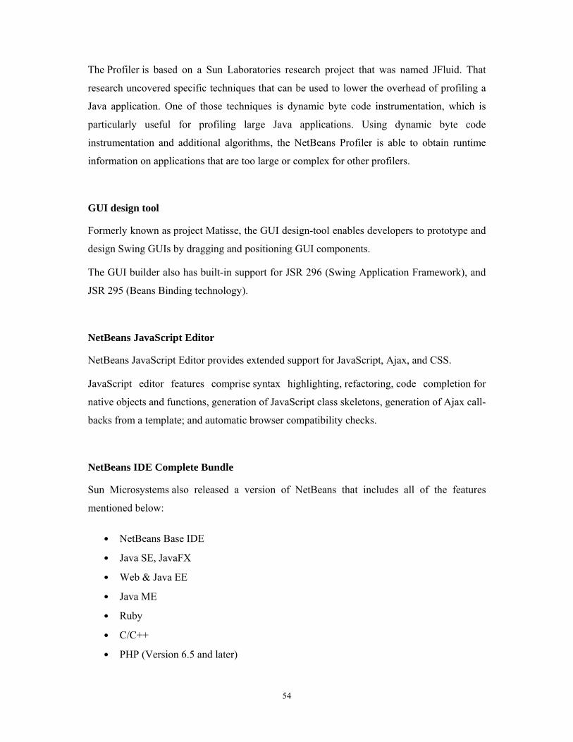
54
The Profiler is based on a Sun Laboratories research project that was named JFluid. That
research uncovered specific techniques that can be used to lower the overhead of profiling a
Java application. One of those techniques is dynamic byte code instrumentation, which is
particularly useful for profiling large Java applications. Using dynamic byte code
instrumentation and additional algorithms, the NetBeans Profiler is able to obtain runtime
information on applications that are too large or complex for other profilers.
GUI design tool
Formerly known as project Matisse, the GUI design-tool enables developers to prototype and
design Swing GUIs by dragging and positioning GUI components.
The GUI builder also has built-in support for JSR 296 (Swing Application Framework), and
JSR 295 (Beans Binding technology).
NetBeans JavaScript Editor
NetBeans JavaScript Editor provides extended support for JavaScript, Ajax, and CSS.
JavaScript editor features comprise syntax highlighting, refactoring, code completion for
native objects and functions, generation of JavaScript class skeletons, generation of Ajax call-
backs from a template; and automatic browser compatibility checks.
NetBeans IDE Complete Bundle
Sun Microsystems also released a version of NetBeans that includes all of the features
mentioned below:
NetBeans Base IDE
Java SE, JavaFX
Web & Java EE
Java ME
Ruby
C/C++
PHP (Version 6.5 and later)

55
Glassfish
Apache Tomcat
6.2 WSN 1.0 GUI
WSN 1.0 is general purpose GUI software made in NetBeans which enables interfacing of
PC with wireless node via USB port. It uses rxtxSerial.dll file which has inbuilt functions to
communicate with USB port. Data in serial form is sent and received through USB COM port
can be accessed using WSN 1.0
Features of WSN 1.0:
• COM port selection
• Data rate selection
• File/Text data transmission option
• Preserves file format as it is
• Large text area to view received data
• GUI can be easily modified
*Refer APPENDIX B for source code.
6.2.1 WSN 1.0 GUI development in NetBeans WSM 1.0 uses serial communication library files to access USB port of the PC. It has powerful built in functions to communicate with serial port. SerialPortEventListener: This function is responsible for communication with serial port of the PC. All the configuration of COM port as well as data rate settings are accomplished in this function CommPortIdentifier: It identifies COM port at where wireless node is connected SerialPortEvent: All the events that occurs is to be written in this function
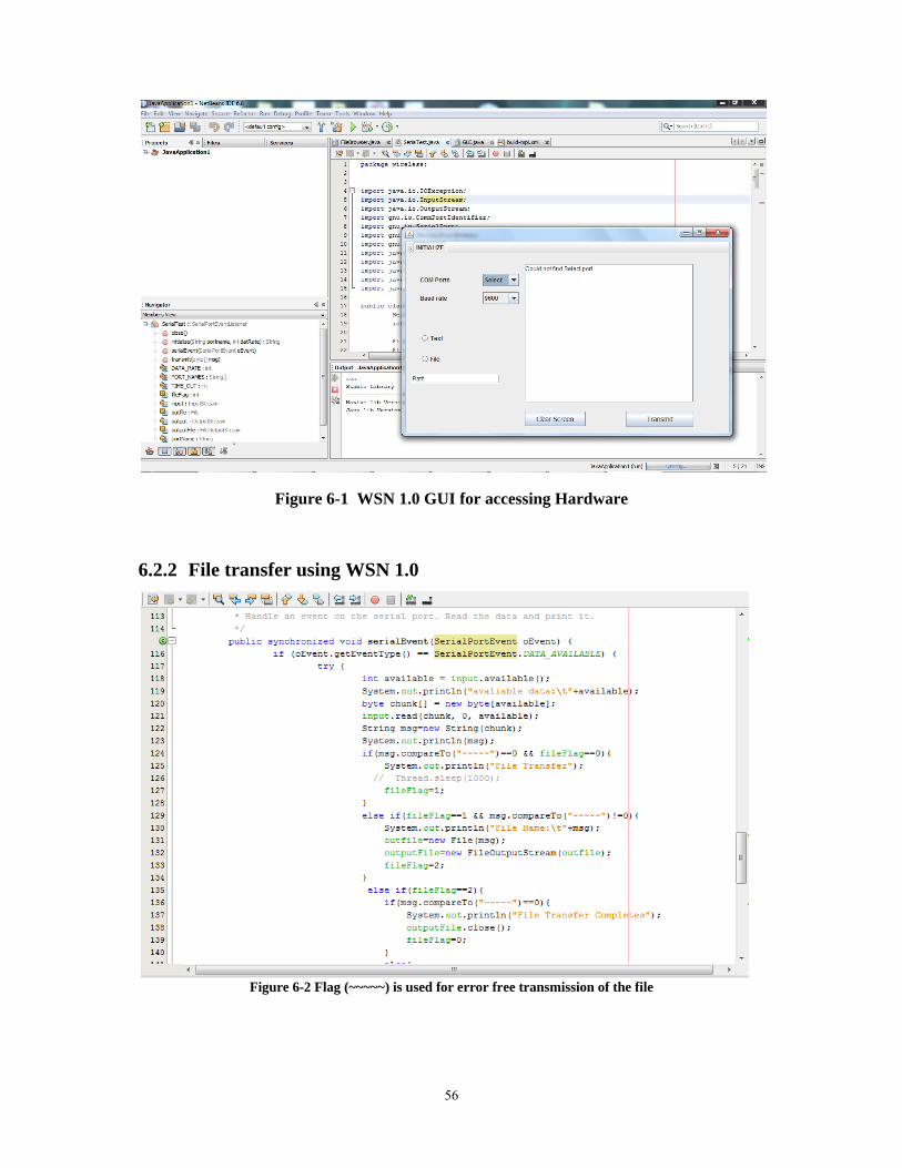
56
Figure 6-1 WSN 1.0 GUI for accessing Hardware
6.2.2 File transfer using WSN 1.0
Figure 6-2 Flag (~~~~~) is used for error free transmission of the file
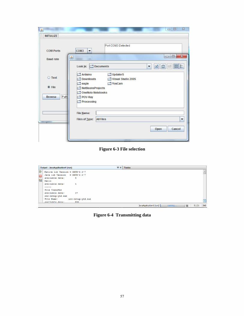
57
Figure 6-3 File selection
Figure 6-4 Transmitting data

58
7 APPLICATIONS

59
7.1 Applications
Some fields where wireless sensor networks find widespread applications are listed below.
These applications are feasible using ZigBee, which allows data rate of 250kbps. For that
specialized speech coding is required to compress the data. Types of streaming are as
follows:
Unicast protocols send a separate copy of the media stream from the server to each
recipient. Unicast is the norm for most Internet connections, but does not scale well
when many users want to view the same program concurrently.
Multicast protocols were developed to reduce the data replication (and consequent
server/network loads) that occurs when many recipients receive Unicast content
streams independently. These protocols send a single
1. File Transfer
File transfer is a generic term for the act of transmitting files over a computer network or
the Internet. There are numerous ways and protocols to transfer files over a network.
Computers which provide a file transfer service are often called file servers. Depending on
the client's perspective the data transfer is called uploading or downloading.
There are 2 types of file transfers:
Pull-based file transfers where the receiver initiates a file transmission request.
Push-based file transfers where the sender initiates a file transmission request.
Here the data transfer is initiated by the sender so it is called Push-based. The protocol used
from the large pool of protocols is ZigBee, which allows 250kbps with very low power
consumption. File of any format (Text, Audio etc.) can be transferred over air from one
computer terminal to the other using the application. A dedicated GUI (Graphical User
Interface) is designed such that it allows the direct text chatting and an additional option to
select the desired file to transferred is also provided.

60
2. Live Media streaming
The verb 'to stream' is also derived from this term, meaning to deliver media in this
manner. Streaming media are multimedia that are constantly received by, and
normally presented to, an end-user while being delivered by a streaming provider.
Live streaming of audio is stream from the source to a group of recipients. Depending
on the network infrastructure and type, multicast transmission may be feasible.
Peer-to-peer (P2P) protocols arrange for prerecorded streams to be sent between
computers. This prevents the server and its network connections from becoming a
bottleneck. However, it raises technical, performance, quality, and business issues.
3. Seismic Structure Response
• Science
- Understand response of buildings and underlying soil to ground shaking.
- Develop models to predict structure response for earthquake scenarios.
• Techniques and Applications
- Identification of seismic events that cause significant structure shaking.
- Local, at-node processing of waveforms.
- Embedded Network Sensing (ENS) [2] will provide field data at sufficient densities to
develop predictive models of structure, foundation, soil response.
4. Contaminant Transport
• Science
- Understand inter-media contaminant transport and fate in real systems.
- Identify risky situations before they become exposures. Subterranean deployment.
• Techniques
- Environmental Micro-Sensors.
- Sensors capable of recognizing phases in air/water/soil mixtures.
- Sensors that withstand physically and chemically harsh conditions.
- Signal Processing: Nodes capable of real-time analysis of signals.
- Collaborative signal processing to expend energy only where there is risk.

61
5. Ecosystem Monitoring
• Science
- Understand response of wild populations to habitats over time.
- Develop in situ observation of species and ecosystem dynamics.
• Techniques
- Data acquisition of physical and chemical properties, at various spatial and temporal
scales, appropriate to the ecosystem, species and habitat.
- Automatic identification of organisms (current techniques involve close-range
human observation).
- Measurements over long period of time, taken in-situ. Harsh environments with
extremes in temperature, moisture, obstructions etc.
6. Context Aware Home
The goal of research on context-aware buildings[3] is to offer an unobtrusive and appealing
environment embedded with pervasive devices that help its occupants to achieve their tasks at
hand; technology that interacts closely with its occupants in the most natural ways to the
point where such interaction becomes implicit. A multitude of futuristic scenarios have been
prophesied in magazines, movies and research papers. Researchers and technologists are
often very cautious in predicting the future shape of our technological landscape but the
following simple scenarios are among the recurring visions:
• Lights, chairs and tables automatically adjust as soon as the family gathers in the living
room to watch TV.
• Phones only ring in rooms where the addressee is actually present, preventing other
people being disturbed by useless ringing.
• The music being played in a room adapts automatically to the people within and the
pictures in the frames on the desk change depending on which person is working there.
• Interactive play spaces are created for children where images, music, narration, light and
sound effects are used to transform a normal child's bedroom into a fantasy land.
• In-house context-aware communication systems allow family members to speak to each
other as if they were in the same room, even when they are in different rooms.
• Elderly people will be supported in their daily life by context-aware homes, allowing
them to age in their own home or familiar environment.

62
• Complete security systems including emergency call out alarms for burglars, fire, or
injury with a complete awareness of the home owners wherever they are.
Figure 7-1 Context Aware Home
• In assisted living complexes, context-aware systems monitor the state of the elderly
occupants, freeing the nursing staff from the task of constantly supervising them, thus
giving them more time to care about those who actually need their support most.

63
8 RESULTS AND CONCLUSION

64
RESULTS
The designed hardware was fabricated and tested several times for various parameters to
determine the range, reliability, sensitivity and amount of power reduction achieved. The
results were highly encouraging and have been summarized below.
Reliability
The hardware designed is highly reliable. The hardware delivered satisfactory
performance for almost 100% of the time. Out of an approximate 50 times that the
hardware was switched on for operation, it functioned 49 times perfectly as it should be
working.
Power Consumption
The results obtained are comparable to industrial and commercial standards. The
electrical current consumption in various modes has been summarized in the following
table:
Table 2 Observation of Current Consumption
Mode Current Consumption
Transmit 11.5 mA
Receive 10.6 mA
Sleep 160 µA
Range
During testing a range of 100m (LOS) was achieved. It worked indoor range of 10m as
desired. However, keeping in mind that power transmitted has been limited to the
minimum since numerous such low power sensors will be deployed in the same area, it is
safe to assume that the range available is satisfactory.

65
CONCLUSION
The designed hardware conforms to the requirements detailed in the previous chapters
and performs with high reliability. The results obtained on testing the hardware are
satisfactory and the design is ready to be scaled for a full fledged Wireless Sensor
Network. The objective of power reduction in the nodes has been realized. With the use
of more sophisticated fabrication of the hardware this design is ideal to be used for
implementation of various commercial and industrial applications.
With regard to WSNs we may conclude that they have the potential to transform
communications. Integrating WSNs with existing services is also a possibility which
promises to usher in a revolution in communication technology. Unlike other networks,
WSNs are designed for specific applications. Applications include, but are not limited to,
environmental monitoring, surveillance systems, military target tracking and context
aware homes. In the future, WSNs are expected to become integral parts of our lives
through various such applications. Each application differs in features and requirements.
To support this diversity of applications, the development of new communication
protocols, algorithms, designs, and services are needed.

66
REFERENCES
[1] Yingshu Li, My T. Thai, Weili Wu, “Wireless Sensor Networks and Applications”,
Springer Science Media, LLC, 2008.
[2] Mohammad Ilyas, Imad Mahgoub, “Handbook of Sensor Networks: Compact Wireless
and Wired Sensing Systems”, CRC Press, 2005.
[3] Sven Meyer, Andry Rakotonirainy, “A Survey of Research on Context-Aware Homes”.
[4] XBow Technologies: http://www.xbow.com/Products/wproductsoverview.aspx
[5] Arduino: An open hardware: http://www.arduino.cc/
[6] Bootloader (Wikipedia): http://en.wikipedia.org/wiki/Booting
[7] Xbee: http://www.digi.com/products/wireless/zigbee-mesh/xbee-zb-module.jsp#overview
[8]Atmega168Datasheet: http://www.atmel.com/dyn/resources/prod_documents/doc2545.pdf
[9]FT232R Datasheet: http://www.ftdichip.com/Documents/DataSheets/DS_FT232R.pdf
[10] NetBeans: www.netbeans.org/
[11] X-CTU: http://x-ctu.software.informer.com/
[12] ZigBee Protocol: http://en.wikipedia.org/wiki/ZigBee
[13] USB Protocol: http://en.wikipedia.org/wiki/Universal_Serial_Bus

67
APPENDIX A:
PCB LAYOUTS
Figure 8-1 Top copper layer component side
Figure 8-2 Bottom copper layer solder side
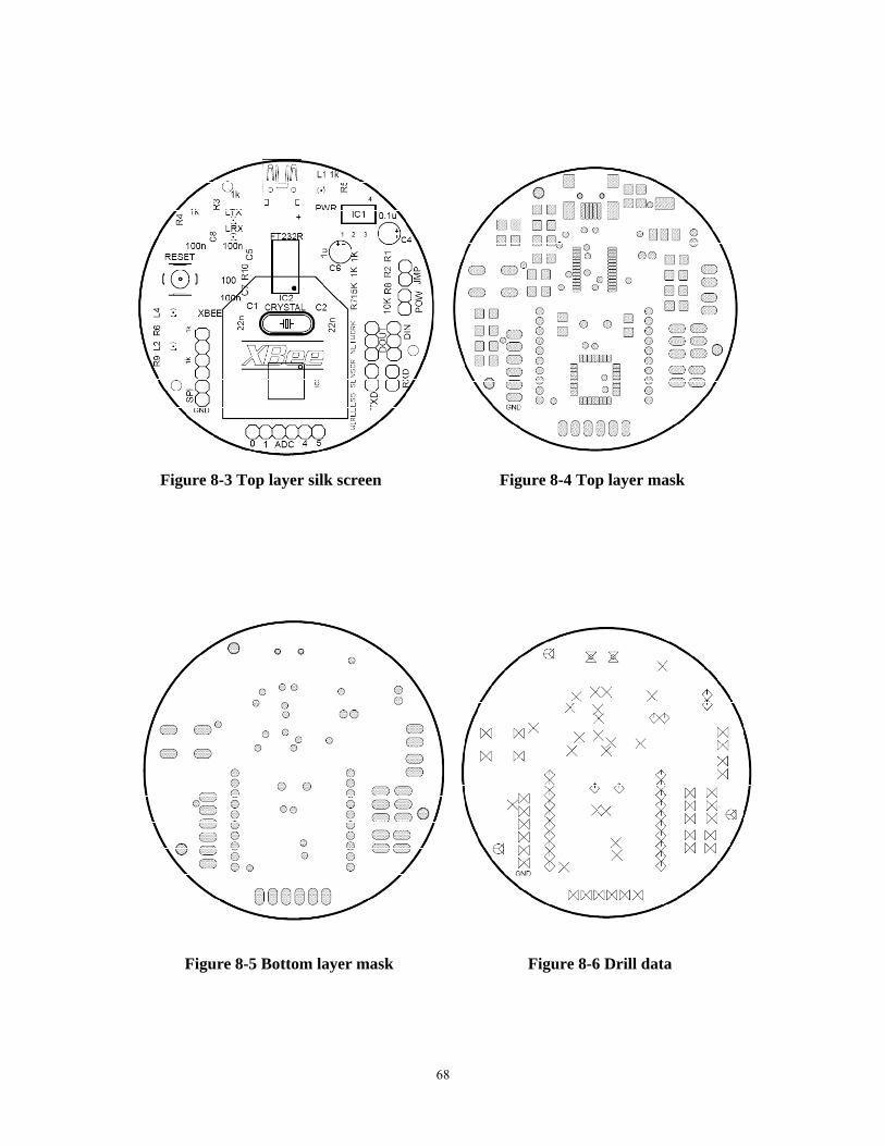
68
Figure 8-3 Top layer silk screen Figure 8-4 Top layer mask
Figure 8-5 Bottom layer mask Figure 8-6 Drill data

69
Figure 8-7 Test PCB

70
APPENDIX B:
JAVA Interfacing Code
/* This Code uses SerialTXRX Library to access USB port of the PC. It creates Virtual COM
port on USB. Data available on USB port is serial data */
package wireless;
import java.io.IOException;
import java.io.InputStream;
import java.io.OutputStream;
import gnu.io.CommPortIdentifier;
import gnu.io.SerialPort;
import gnu.io.SerialPortEvent;
import gnu.io.SerialPortEventListener;
import java.io.File;
import java.io.FileOutputStream;
import java.util.Enumeration;
import java.util.logging.Level;
import java.util.logging.Logger;
public class SerialTest implements SerialPortEventListener {
SerialPort serialPort;
int fileFlag;
File outfile;
FileOutputStream outputFile;
/** The port we're normally going to use. */
private static final String PORT_NAMES[] = {
"COM5", // Windows
"COM4",
"COM3",
"COM1"
};
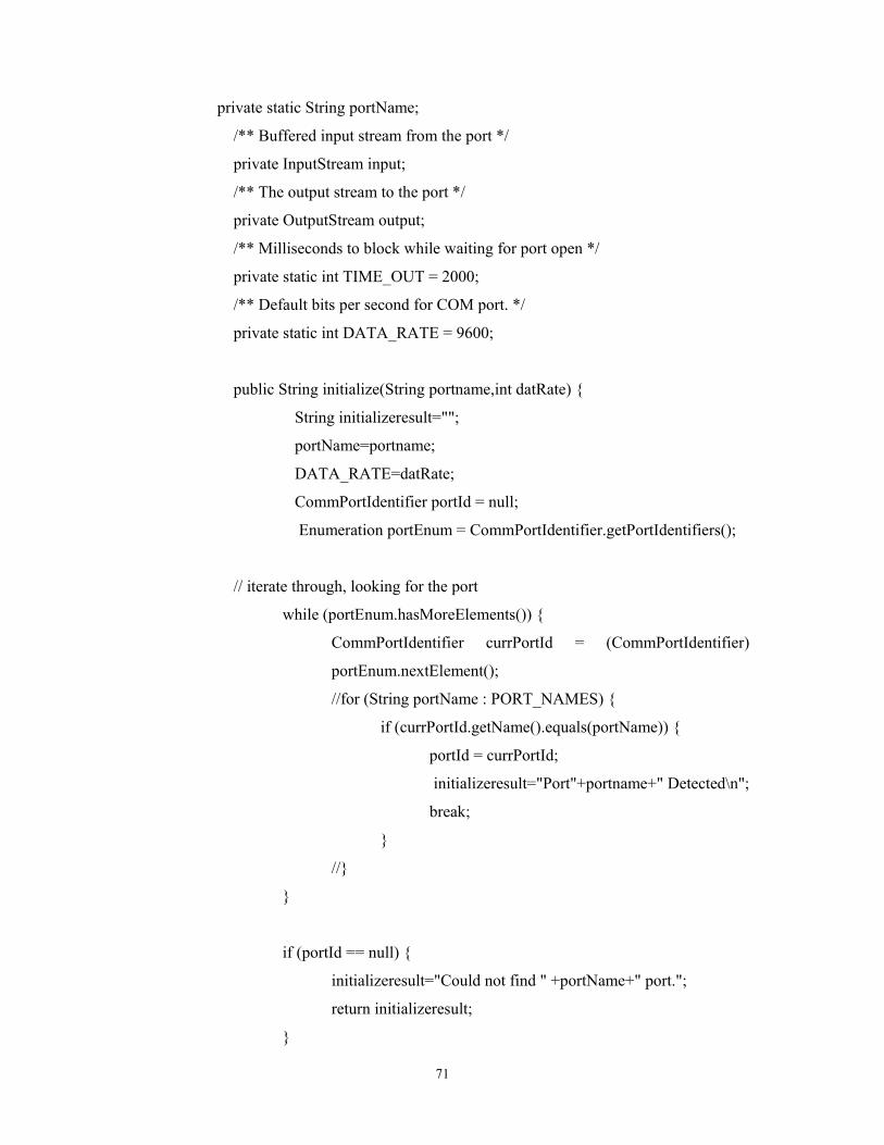
71
private static String portName;
/** Buffered input stream from the port */
private InputStream input;
/** The output stream to the port */
private OutputStream output;
/** Milliseconds to block while waiting for port open */
private static int TIME_OUT = 2000;
/** Default bits per second for COM port. */
private static int DATA_RATE = 9600;
public String initialize(String portname,int datRate) {
String initializeresult="";
portName=portname;
DATA_RATE=datRate;
CommPortIdentifier portId = null;
Enumeration portEnum = CommPortIdentifier.getPortIdentifiers();
// iterate through, looking for the port
while (portEnum.hasMoreElements()) {
CommPortIdentifier currPortId = (CommPortIdentifier)
portEnum.nextElement();
//for (String portName : PORT_NAMES) {
if (currPortId.getName().equals(portName)) {
portId = currPortId;
initializeresult="Port"+portname+" Detected\n";
break;
}
//}
}
if (portId == null) {
initializeresult="Could not find " +portName+" port.";
return initializeresult;
}
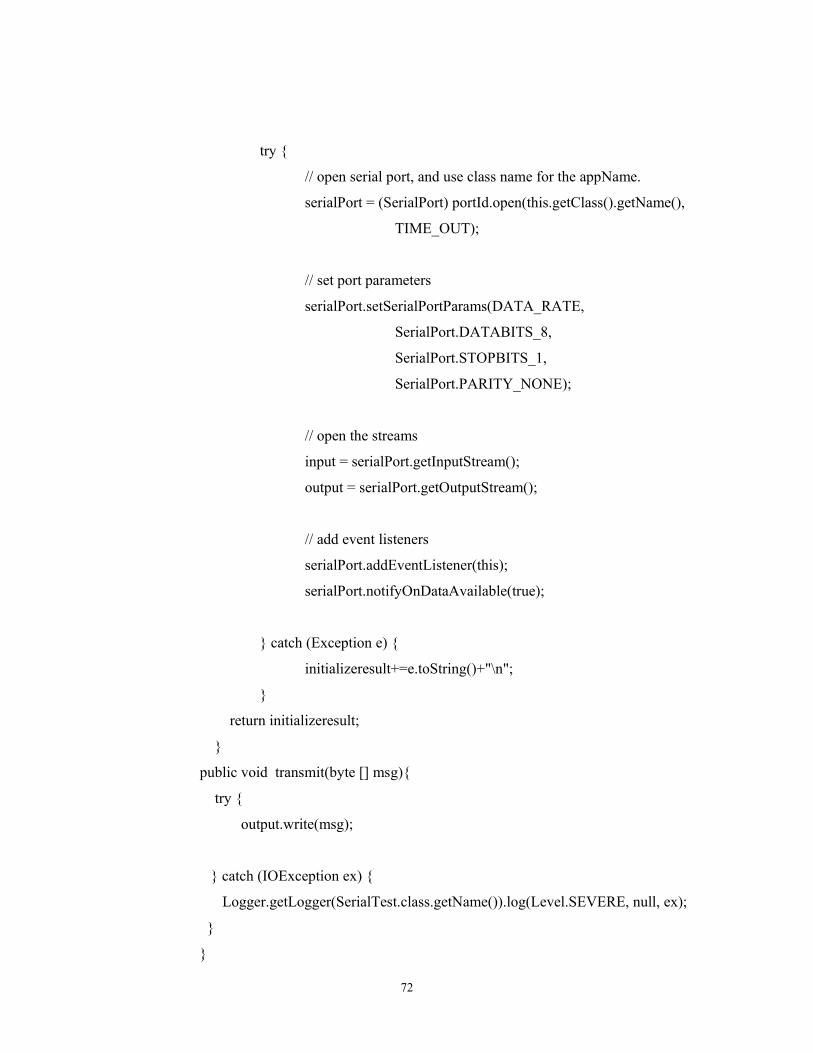
72
try {
// open serial port, and use class name for the appName.
serialPort = (SerialPort) portId.open(this.getClass().getName(),
TIME_OUT);
// set port parameters
serialPort.setSerialPortParams(DATA_RATE,
SerialPort.DATABITS_8,
SerialPort.STOPBITS_1,
SerialPort.PARITY_NONE);
// open the streams
input = serialPort.getInputStream();
output = serialPort.getOutputStream();
// add event listeners
serialPort.addEventListener(this);
serialPort.notifyOnDataAvailable(true);
} catch (Exception e) {
initializeresult+=e.toString()+"\n";
}
return initializeresult;
}
public void transmit(byte [] msg){
try {
output.write(msg);
} catch (IOException ex) {
Logger.getLogger(SerialTest.class.getName()).log(Level.SEVERE, null, ex);
}
}

73
public synchronized void close() {
if (serialPort != null) {
serialPort.removeEventListener();
serialPort.close();
}
}
/*
* Handle an event on the serial port. Read the data and print it.
*/
public synchronized void serialEvent(SerialPortEvent oEvent) {
if (oEvent.getEventType() == SerialPortEvent.DATA_AVAILABLE)
{
try {
int available = input.available();
System.out.println("avaliable data:\t"+available);
byte chunk[] = new byte[available];
input.read(chunk, 0, available);
String msg=new String(chunk);
System.out.println(msg);
if(msg.compareTo("~~~~~")==0 && fileFlag==0){
System.out.println("File Transfer");
// Thread.sleep(1000);
fileFlag=1;
}
else if(fileFlag==1 && msg.compareTo("~~~~~")!=0){
System.out.println("File Name:\t"+msg);
outfile=new File(msg);
outputFile=new FileOutputStream(outfile);
fileFlag=2;
}
else if(fileFlag==2){
if(msg.compareTo("~~~~~")==0){

74
System.out.println("File Transfer Completes");
outputFile.close();
fileFlag=0;
}
else{
outputFile.write(chunk);
}
//System.out.println(msg);
}
else{
new MyMain().getMsg(chunk);
}
} catch (Exception e) {
System.err.println(e.toString());
}
}
if(oEvent.getEventType()==SerialPortEvent.OUTPUT_BUFFER_EMPTY){
System.out.println("rpam");
}
// Ignore all the other eventTypes, but you should consider the other
ones.
}
}

75
APPENDIX C:
BILL OF MATERIALS
Name Quantity Price
1. Printed circuit Board 4 1390 INR
2. XBEE 2 3233 INR
3. FT232R 2 700 INR
4. ATmega168 2 700 INR
5. LM2937 2 70 INR
6. Arduino Board 1 1400 INR
7. USB Cable 2 120 INR
8. Prototype PCB 2 300 INR
9. 1k Resistor SMD – 1206 16 16 INR
10. 20 MHz XTAL 2 40 INR
11. Male Header 3 48 INR
12. Push Switch 2 10 INR
13. LED SMD – 1206 12 36 INR
14. Capacitor SMD – 100n -
1206 10 10 INR
15. Capacitor – 0.1uF 4 8 INR
16. Miscellaneous - 200 INR
17. Jumper 12 24 INR
18. 5V Battery 1 200 INR
Total 8512 INR

76
APPENDIX D:
RESOURCES
Resources Used:
• In System Programmer (For Programming of ATmega168)
• 2 Computer Terminals
• Soldering Iron
• Solder
• Flux
• Pliers
• Multimeter
Software Tools Used:
• WinAVR - For Microcontroller Programming
• JAVA – JRE and JDK - For GUI Development
• NetBeans IDE 6.8 - For GUI Development
• FTDI USB Drivers (www.ftdichip.com) - FT232R IC Drivers
• FT_PROG v1.3.1 (www.ftdichip.com) - Testing FT232R IC
• X-CTU (www.digi.com) - Testing XBEE Modules
• Arduino_Software_V_0018 (www.arduino.cc) – For Programming
Microcontroller
• Eagle-5.7.0 - For PCB Layout Design
• Eagle3D - 3D Simulated view of PCB
• POVray - 3D PCB diagram generator
• AVRdude - To burn Microcontroller

77
APPENDIX E:
STEPS TO RUN HARDWARE • Connect Node to PC using USB cable
• Install FTDI USB Drivers
• Select Jumper settings for XBEE Configuration. XBEE status LED is blinking.
• Run X-CTU Software and select appropriate Baud Rate and other settings
• Now select Jumper settings for Controller programming, Using USB programmer
program the controller as per the application requirement.
• Run GUI – WSN 1.0
• Click on INITIALIZE the hardware. It will scan the device and will automatically
update COM port.
• Transmit and Receive data…..

78
IEEE CODE OF ETHICS
We, the members of the IEEE, in recognition of the importance of our technologies in affecting the quality of life throughout the world, and in accepting a personal obligation to our profession, its members, and the communities we serve, do hereby commit ourselves to the highest ethical and professional conduct and agree: 1. To accept responsibility in making decisions consistent with the safety, health and
welfare of the public, and to disclose promptly factors that might endanger the public of the environment;
2. To avoid real or perceived conflicts of interest whenever possible, and to disclose them to affected parties when they do exist;
3. To be honest and realistic in stating claims or estimates based on available data; 4. To reject bribery in all its forms; 5. To improve on the understanding of technology, its appropriate application, and
potential consequences; 6. To maintain and improve our technical competencies and to undertake technological
tasks for others only if qualified by training or experience, or after full disclosure of pertinent limitations;
7. To seek, accept and offer honest criticism of technical work, to acknowledge and correct errors, and to credit properly the contributions of others;
8. To treat fairly all persons regardless of such factors as race, religion, gender, disability, age, or national origin;
9. To avoid injuring others, their property, reputation, or employment by false or malicious action;
10. To assist colleagues and co-workers in their professional development and to support them in following this code of ethics.
The IEEE code of ethics applies in multiple ways to our Minor Project experience. First, being honest and realistic in stating claims or estimates was extremely important to our project’s scope. Since our research will serve as background knowledge for other researchers in this area, we strived not to exaggerate our findings. Being conservative in estimates is a practice that every engineer should adopt, not just IEEE members. Furthermore, as we often presented the progress of our project work to faculty members of Nirma University, we were put in positions to give and receive constructive criticisms. It was important for us that these criticisms be received in a professional manner. Finally, our project focused on improving the understanding of technology and its appropriate applications. By writing this detailed report, we are furthering the understanding of the technology we have researched and making it easier for other engineers to understand our project.