wireless power receiver and 400ma buck battery …this technique modulates the resonant frequency of...
TRANSCRIPT

LTC4120
14120fa
For more information www.linear.com/LTC4120
Typical applicaTion
FeaTures DescripTion
Wireless Power Receiver and 400mA Buck Battery Charger
The LTC®4120 is a constant-current/constant-voltage wireless receiver and battery charger. An external program-ming resistor sets the charge current up to 400mA. The programmable float voltage of the LTC4120 accommodates several battery chemistries. The LTC4120 uses a Dynamic Harmonization Control (DHC) technique that allows high efficiency contactless charging across an air gap.
The LTC4120 regulates its input voltage via the DHC pin. This technique modulates the resonant frequency of a receiver tank to automatically adjust the power received as well as the power transmitted to provide an efficient solution for wirelessly charging battery-powered devices.
Wireless charging with the LTC4120 provides a method to power devices in harsh environments without requiring expensive failure-prone connectors. This allows products to be charged while locked within sealed enclosures, or in moving or rotating equipment, or where cleanliness or sanitation is critical.
This full featured battery charger includes accurate RUN pin threshold, low voltage battery preconditioning and bad battery fault detection, timer termination, auto-recharge, and NTC temperature qualified charging. The FAULT pin provides an indication of bad battery or temperature faults.
Once charging is terminated, the LTC4120 signals end-of-charge via the CHRG pin, and enters a low current sleep mode. An auto-restart feature starts a new charging cycle if the battery voltage drops by 2.5%.
applicaTions
n Dynamic Harmonization Control Optimizes Wireless Charging Over a Wide Coupling Range
n Wide Input Voltage Range: 4.3V to 40Vn Adjustable Battery Float Voltage: 3.5V to 11Vn 50mA to 400mA Charge Current Programmed with a
Single Resistorn ±1% Feedback Voltage Accuracyn Programmable 5% Accurate Charge Currentn No Microprocessor Requiredn No Transformer Coren Thermally Enhanced, Low Profile 16-Lead
(3mm × 3mm × 0.75mm) QFN Package
n Handheld Instrumentsn Industrial/Military Sensors and Devicesn Harsh Environmentsn Portable Medical Devicesn Physically Small Devicesn Electrically Isolated DevicesL, LT, LTC, LTM, Linear Technology, the Linear logo and Burst Mode are registered trademarks of Linear Technology Corporation. All other trademarks are the property of their respective owners.
+
INTVCCINFREQRUN
BOOST
SW
CHGSNS
NTC
DHC
FAULT
CHRG
3.01k 10µF
T
4120 TA01a
Li-Ion4.2V
22nF
26.7nF
6.5nF
47µH5µH
Tx CIRCUITRY
10µF
2.2µF
33µH
FB
PROG FBG
LTC4120
GND
BAT
1.01M
1.35M
Wireless Rx Voltage/Charge Current vs Spacing
SPACING (cm)0.4
V IN(
RX) (
V)
CHARGE CURRENT (mA)
30
35
40
1.0 1.4
4120 TA01b
25
20
0.6 0.8 1.2 1.6 1.8
VIN
15
10
200
267
333
400
133
67
0
ICHARGEMAX
NOTCHARGING
CHARGING

LTC4120
24120fa
For more information www.linear.com/LTC4120
pin conFiguraTionabsoluTe MaxiMuM raTings
IN, RUN, CHRG, FAULT, DHC ...................... –0.3V to 43VBOOST ................................... VSW – 0.3V to (VSW + 6V)SW (DC) ........................................ –0.3V to (VIN + 0.3V)SW (Pulsed <100ns) ......................–1.5V to (VIN + 1.5V)CHGSNS, BAT, FBG, FB ...............................–0.3V to 12VFREQ, NTC, PROG, INTVCC .......................... –0.3V to 6VICHGSNS, IBAT ..................................................... ±600mAIDHC ............................................................... 350mARMSICHRG, IFAULT, IFBG ..................................................±5mAIFB .........................................................................±5mAIINTVCC .................................................................. –5mAOperating Junction Temperature Range (Note 2) .................................................. –40°C to 125°CStorage Temperature Range .................. –65°C to 150°C
(Note 1)
orDer inForMaTionLEAD FREE FINISH TAPE AND REEL PART MARKING* PACKAGE DESCRIPTION TEMPERATURE RANGE
LTC4120EUD#PBF LTC4120EUD#TRPBF LGHB 16-Lead (3mm × 3mm) Plastic QFN –40°C to 125°C
LTC4120IUD#PBF LTC4120IUD#TRPBF LGHB 16-Lead (3mm × 3mm) Plastic QFN –40°C to 125°C
Consult LTC Marketing for parts specified with wider operating temperature ranges. *The temperature grade is identified by a label on the shipping container.
Consult LTC Marketing for information on nonstandard lead based finish parts.For more information on lead free part marking, go to: http://www.linear.com/leadfree/ For more information on tape and reel specifications, go to: http://www.linear.com/tapeandreel/
16 15 14 13
5 6 7 8
TOP VIEW
17GND
UD PACKAGE16-LEAD (3mm × 3mm) PLASTIC QFN
9
10
11
12
4
3
2
1INTVCC
BOOST
IN
SW
NTC
FBG
FB
BAT
RUN
FAUL
T
CHRG
PROG
GND
DHC
FREQ
CHGS
NS
TJMAX = 125°C, θJA = 54°C/W
EXPOSED PAD (PIN 17) IS GND, MUST BE SOLDERED TO PCB TO OBTAIN θJA

LTC4120
34120fa
For more information www.linear.com/LTC4120
elecTrical characTerisTics The l denotes the specifications which apply over the full operating junction temperature range, otherwise specifications are at TA = 25°C (Note 2). VIN = VRUN = 15V, VCHGSNS = VBAT = 4V, RPROG = 3.01k, VFB = 2.29V. Current into a pin is positive out of the pin is negative.
SYMBOL PARAMETER CONDITIONS MIN TYP MAX UNITS
VIN Operating Input Supply Range l 4.3 40 V
VBAT Battery Voltage Range 0 11 V
IIN DC Supply Current Switching, FREQ = GND 3.5 mA
Standby Mode (Note 3) l 130 220 µA
Sleep Mode (Note 3) VFB = 2.51V (Note 3)
l
60
100
µA
Disabled Mode (Note 3) l 37 70 µA
Shutdown Mode (Note 3) l 20 40 µA
∆VDUVLO Differential Undervoltage Lockout VIN-VBAT Falling, VIN = 5V l 25 80 160 mV
Hysteresis VIN-VBAT Rising, VIN = 5V l 80 115 175 mV
UVINTVCC INTVCC Undervoltage Lockout INTVCC Rising, VIN = INTVCC + 100mV, VBAT = NC l 4.00 4.15 4.26 V
Hysteresis INTVCC Falling 220 mV
VINTVCC INTVCC Regulated Voltage l 4.14 4.24 4.29 V
∆INTVCC INTVCC Load Regulation IINTVCC = 0mA to –5mA (Note 4) 1.7 %
Battery Charger
IBAT BAT Standby Current Standby Mode (Notes 3, 7, 8) l 2.5 4.5 µA
BAT Shutdown Current Shutdown Mode (Notes 3, 7, 8) l 1100 2000 nA
IFB Feedback Pin Bias Current (LTC4120) VFB = 2.5V (Note 7) l 15 50 nA
IFBG(LEAK) Feedback Ground Leakage Current Shutdown Mode (Notes 3, 7) l 1 µA
RFBG Feedback Ground Return Resistance l 1000 2000 Ω
VFB(REG) Feedback Regulation Voltage (Note 5)
l
2.393 2.370
2.400 2.407 2.418
V V
ICHG Battery Charge Current RPROG = 3.01k RPROG = 24.3k
l
l
383 45
401 50
421 55
mA mA
VUVCL Undervoltage Current Limit VIN Falling 12.0 V
VRCHG Battery Recharge Threshold VFB Falling Relative to VFB_REG l –42 –52 –62 mV
hPROG Ratio of BAT Current to PROG Current 988 mA/mA
VPROG PROG Pin Servo Voltage l 1.210 1.222 1.245 V
RSNS CHGSNS-BAT Sense Resistor IBAT = –100mA 300 mΩ
ILOWBAT Low Battery Linear Charge Current 0V < VFB < VTRKL, VBAT = 2.6V 6 10 16 mA
VLOWBAT Low Battery Threshold Voltage VBAT Rising Hysteresis
l 2.15 2.21 143
2.28 V mV
ITRKL Switch Mode Trickle Charge Current VFB < VTRKL, VBAT > VLOWBAT ICHG/10 mA
VPROG(TRKL) PROG Pin Servo Voltage in Switch Mode Trickle Charge
VBAT > VLOWBAT, 1.22V < VTRKL 120 mV
VTRKL Trickle Charge Threshold VFB Rising (Note 5) l 1.66 1.68 1.70 V
Hysteresis VFB Falling (Note 5) 45 mV
hC/10 End of Charge Indication Current Ratio (Note 6) 0.1 mA/mA
Timer Safety Timer Termination Period l 1.3 2.0 2.8 Hours
Bad Battery Termination Timeout l 19 30 42 Minutes

LTC4120
44120fa
For more information www.linear.com/LTC4120
elecTrical characTerisTics The l denotes the specifications which apply over the full operating junction temperature range, otherwise specifications are at TA = 25°C (Note 2). VIN = VRUN = 15V, VCHGSNS = VBAT = 4V, RPROG = 3.01k, VFB = 2.29V. Current into a pin is positive out of the pin is negative.
SYMBOL PARAMETER CONDITIONS MIN TYP MAX UNITS
Switcher
fOSC Switching Frequency FREQ = INTVCC FREQ = GND
l
l
1.10 0.56
1.35 0.71
1.75 0.81
MHz MHz
tMIN(ON) Minimum Controllable On-Time (Note 9) 120 ns
DC Duty Cycle Maximum (Note 9) l 94 %
RDS(ON)TOP Top Switch RDS(ON) ISW = –100mA 0.7 Ω
RDS(ON)BOT Bottom Switch RDS(ON) ISW = 100mA 0.35 Ω
IPEAK Peak Current Limit Measured Across RSNS with a 15µH Inductor in Series with RSNS (Note 9)
585 750 1250 mA
ISW Switch Pin Current (Note 8) VIN = Float, VRUN = 0V, VSW = 8.4V l 15 30 µA
Status Pins FAULT, CHRG
VOL Pin Output Voltage Low I = 2mA 500 mV
ILEAK Pin Leakage Current V = 45V, Pin High Impedance 0 1 µA
NTC
VTOO_COLD Cold Temperature VNTC/VINTVCC Fault Rising VNTC Threshold Falling VNTC Threshold
l 73 74 72
75 %INTVCC %INTVCC
VTOO_HOT Hot Temperature VNTC/VINTVCC Fault Falling VNTC Threshold Rising VNTC Threshold
l 35.5 36.5 37.5
37.5 %INTVCC %INTVCC
VDIS NTC Disable Voltage Falling VNTC Threshold Rising VNTC Threshold
l 1 2 3
3 %INTVCC %INTVCC
INTC NTC Input Leakage Current VNTC = VINTVCC –50 50 nA
RUN
VEN Enable threshold VRUN Rising l 2.35 2.45 2.55 V
Hysteresis VRUN Falling 200 mV
IRUN Run Pin Input Current VRUN = 40V 0.01 0.1 µA
VSD Shutdown Threshold (Note 3) VRUN Falling l 0.4 1.2 V
Hysteresis 220 mV
FREQ
VIL FREQ Pin Input Low l 0.4 V
VIH FREQ Pin Input High VINTVCC-VFREQ l 0.6 V
IFREQ FREQ Pin Input Current 0V < VFREQ < VINTVCC ±1 µA
Dynamic Harmonization Control
VIN(DHC) Input Regulation Voltage 14 V
IDHC DHC Pin Current VDHC = 1V, VIN < VIN(DHC) 330 mARMS
Note 1: Stresses beyond those listed under Absolute Maximum Ratings may cause permanent damage to the device. Exposure to any Absolute Maximum Rating condition for extended periods may affect device reliability and lifetime.Note 2: The LTC4120 is tested under pulsed load conditions such that TJ ≈ TA. The LTC4120E is guaranteed to meet performance specifications for junction temperatures from 0°C to 85°C. Specifications over the –40°C to 125°C operating junction temperature range are assured by design, characterization and correlation with statistical process controls. The LTC4120I is guaranteed over the full –40°C to 125°C operating junction temperature range. Note that the maximum ambient temperature
consistent with these specifications is determined by specific operating conditions in conjunction with board layout, the rated package thermal impedance, and other environmental factors.Note 3: Standby mode occurs during an NTC fault condition or when FB is at regulation but the timer has not timed out. Disabled mode occurs when VRUN is between VSD and VEN. Shutdown mode occurs when VRUN is below VSD or when the differential undervoltage lockout is engaged.Note 4: The internal supply INTVCC should only be used for the NTC divider, it should not be used for any other loads.Note 5: The FB pin is measured with a resistance of 588k in series with the pin.

LTC4120
54120fa
For more information www.linear.com/LTC4120
elecTrical characTerisTicsNote 6: hC/10 is expressed as a fraction of measured full charge current as measured at the PROG pin voltage when the CHRG pin de-asserts.Note 7: In an application circuit with an inductor connected from SW to CHGSNS, the total battery leakage current when disabled is the sum of IBAT, IFBG and ISW.
Typical perForMance characTerisTics
Typical VFB(REG) vs Temperature
ICCQ Disabled/Shutdown vs Temperature
IBAT Sleep/Shutdown vs Temperature ICHARGE vs Temperature
IIN Standby/Sleep vs Temperature
TA = 25°C, unless otherwise noted.
Note 8: When no supply is present at IN, the SW powers IN through the body diode of the topside switch. This may cause additional SW pin current depending on the load present at IN.Note 9: Guaranteed by design and/or correlation to static test.
TEMPERATURE (°C)–40
2.36
V FB(
REG)
(V)
2.37
2.39
2.40
2.41
2.43
–25 35 65
4120 G01
2.38
2.42
20 95 125
DUT = DEVICEUNDER TEST
110–10 5 50 80
4 UNITS TESTED
HIGH LIMITDUT1 VFB(REG) (V)DUT2 VFB(REG) (V)DUT3 VFB(REG) (V)DUT4 VFB(REG) (V)LOW LIMIT
TEMPERATURE (°C)–50
120
140
180
25 75
4120 G02
100
80
–25 0 50 100 125
60
40
160
I IN (µ
A)
2 UNITS TESTEDVIN = 15V
IIN STANDBY FREQ = INTVCCIIN STANDBY FREQ = INTVCCIIN STANDBY FREQ = GNDIIN STANDBY FREQ = GNDIIN SLEEPIIN SLEEP
TEMPERATURE (°C)–50
I CCQ
(µA)
40
50
60
25 75
4120 G03
30
20
–25 0 50 100 125
10
0
IIN SDIIN SD
IIN DISABLEDIIN DISABLED
2 UNITS TESTEDVIN = 15V
TEMPERATURE (°C)–50
I BAT
(µA)
7
25
4120 G04
4
2
–25 0 50
1
0
8
6
5
3
75 100 125
IBAT SLEEPIBAT SLEEP
IBAT SHUTDOWNIBAT SHUTDOWN
2 UNITS TESTEDVBAT = 4.2VRFB1 = 1.01MRFB2 = 1.35M
TEMPERATURE (°C)–50
399
400
402
25 75
4120 G05
398
397
–25 0 50 100 125
396
395
401
I CHA
RGE
(mA)
FREQ = GNDFREQ = GNDFREQ = INTVCCFREQ = INTVCC
RPROG = 3.01k2 UNITS TESTED

LTC4120
64120fa
For more information www.linear.com/LTC4120
Switching Frequency vs Temperature Buck Efficiency vs Battery Current
Typical tMIN(ON) vs Temperature
Typical perForMance characTerisTics
Wireless Power Transfer Efficiency, VIN_RX vs Battery Current
RSNS Current Limit IPEAK vs Temperature
IBAT Leak/VBAT-VIN vs Temperature
Typical Wireless Charging Cycle
TA = 25°C, unless otherwise noted.
TEMPERATURE (°C)–50
I PEA
K (m
A)
780
800
125
4120 G06
760
740
720
6800 50 100–25 25 75
700
820FREQ = INTVCCFREQ = GND
TEMPERATURE (°C)–50
0.8
1.0
1.4
25 75
4120 G07
0.6
–25 0 50 100 125
0.4
0.2
0
1.2
f SW
(MHz
)FREQ = GNDFREQ = GND
FREQ = INTVCCFREQ = INTVCC
2 UNITS TESTED
IBAT (mA)0
EFFI
CIEN
CY (%
)
75
80
85
400
4120 G08
70
65
60
50100 200 30050 150 250 350
55
95
90
VIN = 12.5VVIN = 14VVIN = 20VVIN = 30V
LSW = 68µH, SLF12555T-680M1R3FREQ = GNDVBAT = 4.2V
TEMPERATURE (°C)–50
I BAT
(µA)
VBAT -V
IN (mV)
14
25
4120 G09
8
4
–25 0 50
2
0
16
12
10
6
350
200
100
50
0
400
300
250
150
75 100 125
IBATIBATVBAT-VINVBAT-VIN
2 UNITS TESTED
VIN = FLOATVBAT = 4.2V
TEMPERATURE (°C)–50
80
t MIN
(0N)
(ns)
85
95
100
105
130
115
0 50 75 100
4120 G10
90
120
125
110
–22 25 125
2 UNITS TESTED
IBAT (mA)0
50
60
70
200
4120 G11
40
30
50 100 150 250
20
10
0
20
22
24
18
16
14
12
10
EFFI
CIEN
CY (%
)
VIN_RX (V)
9mm EFFICIENCY10mm EFFICIENCY11mm EFFICIENCY9mm V_RX10mm V_RX11mm V_RX
VFLOAT = 8.3VLSW = SLF6028-470MR59RPROG = 4.64k
TIME (HOURS)0
0
BATT
ERY
CURR
ENT
(mA)
VBAT , V
CHRG (V)
50
150
200
250
450
4120 G12
100
21 3
300
350
400
0
0.5
1.5
2.0
2.5
4.5
1.0
3.0
3.5
4.0
VCHRG
VBAT
IBAT
BAT = 940mAhrLSW = TDK SLF4075 15µHRFB1 = 732k, RFB2 = 976kRPROG = 3.01kAPPLICATION CCT OF FIGURE 10SPACING = 14mm

LTC4120
74120fa
For more information www.linear.com/LTC4120
Burst Mode Trigger Current
Input Disabled Current vs Input Voltage UVCL: ICHARGE vs Input Voltage
Shutdown Current vs Input Voltage
Typical Burst Mode Waveforms, IBAT = 38mA
Switching Current vs Input Voltage
Typical perForMance characTerisTics TA = 25°C, unless otherwise noted.
VIN (V)10
0
I BAT
(mA)
10
30
40
50
30
90
4120 G13
20
2015 3525 40
60
70
80
RPROG = 6.2k
RPROG = 3k
VSW5V/DIV
VPROG500mV/DIV
ILSW200mA/DIV 0mA
0V
0V
4µs/DIV 4120 G14
VIN (V)0
I IN (µ
A)
40
50
60
40
4120 G15
30
20
010 20 30
10
80
70
IIN SD TEMP = 125°CIIN SD TEMP = 35°CIIN SD TEMP = –40°C
VRUN = 0.6V
VIN (V)0
0
I IN (µ
A)
10
30
40
50
100
70
10 20
4120 G16
20
80
90
60
30 40
IIN SD TEMP = 125°CIIN SD TEMP = 35°CIIN SD TEMP = –40°C
VRUN = 1.6V
VIN (V)5
4
5
7
20 30
4120 G17
3
2
10 15 25 35 40
1
0
6
I IN S
WIT
CHIN
G (m
A)
FREQ = INTVCC
FREQ = GND
VIN (V)11.90
I CHA
RGE
(mA)
0.20
4120 G18
0.10
012.00 12.1011.95 12.05 12.15
0.30
0.40
0.15
0.05
0.25
0.35
12.20
IBAT TEMP = 125°CIBAT TEMP = 35°CIBAT TEMP = –40°C

LTC4120
84120fa
For more information www.linear.com/LTC4120
pin FuncTionsINTVCC (Pin 1): Internal Regulator Output Pin. This pin is the output of an internal linear regulator that generates the internal INTVCC supply from IN. It also supplies power to the switch gate drivers and the low battery linear charge current ILOWBAT. Connect a 2.2µF low ESR capacitor from INTVCC to GND. Do not place any external load on INTVCC other than the NTC bias network. When the RUN pin is above VEN, and INTVCC rises above the UVLO threshold, and IN rises above BAT by ∆VDUVLO and its hysteresis, the charger is enabled.
BOOST (Pin 2): Boosted Supply Pin. Connect a 22nF boost capacitor from this pin to the SW pin.
IN (Pin 3): Positive Input Power Supply. Decouple to GND with a 10µF or larger low ESR capacitor.
SW (Pin 4): Switch Pin. The SW pin delivers power from IN to BAT via the step-down switching regulator. An in-ductor should be connected from SW to CHGSNS. See the Applications Information section for a discussion of inductor selection.
GND (Pin 5, Exposed Pad Pin 17): Ground Pin. Connect to exposed pad. The exposed pad must be soldered to PCB GND to provide a low electrical and thermal impedance connection to ground.
DHC (Pin 6): Dynamic Harmonization Control Pin. Connect a Schottky diode from the DHC pin to the IN pin, and a capacitor from the DHC pin as shown in the Typical Ap-plication or the Block Diagram. When VIN is greater than VIN(DHC), this pin is high impedance. When VIN is below VIN(DHC) this pin is low impedance allowing the LTC4120 to modulate the resonance of the tuned receiver network. See Applications Information for more information on the tuned receiver network.
FREQ (Pin 7): Buck Switching Frequency Select Input Pin. Connect to INTVCC to select a 1.35MHz switching frequency or GND to select a 710kHz switching frequency. Do not float.
CHGSNS (Pin 8): Battery Charge Current Sense Pin. An internal current sense resistor between CHGSNS and BAT pins monitors battery charge current. An inductor should be connected from SW to CHGSNS.
BAT (Pin 9): Battery Output Pin. Battery charge current is delivered from this pin through the internal charge current sense resistor. In low battery conditions a small linear charge current, ILOWBAT, is sourced from this pin to precondition the battery. Decouple the BAT pin with a low ESR 10µF or greater ceramic capacitor to GND.
FB (Pin 10): Battery Voltage Feedback Pin. The charge function operates to achieve a final float voltage of 2.4V at this pin. Battery float voltage is programmed using a resistive divider from BAT to FB to FBG, and can be pro-grammed up to 11V. The feedback pin input bias current, IFB, is 15nA. Using a resistive divider with a Thevenin equivalent resistance of 588k compensates for input bias current error (see curve of FB Pin Bias Current versus Temperature in the Typical Performance Characteristics).
FBG (Pin 11): Feedback Ground Pin. This pin disconnects the external FB divider load from the battery when it is not needed. When sensing the battery voltage this pin pres-ents a low resistance, RFBG, to GND. When in disabled or shutdown modes this pin is high impedance.
NTC (Pin 12): Input to the Negative Temperature Coefficient Thermistor Monitoring Circuit. The NTC pin connects to a negative temperature coefficient thermistor which is typically co-packaged with the battery to determine if the battery is too hot or too cold to charge. If the battery’s temperature is out of range, the LTC4120 enters standby mode and charging is paused until the battery tempera-ture re-enters the valid range. A low drift bias resistor is required from INTVCC to NTC and a thermistor is required from NTC to GND. Tie the NTC pin to GND to disable NTC qualified charging if NTC functionality is not required.

LTC4120
94120fa
For more information www.linear.com/LTC4120
pin FuncTionsPROG (Pin 13): Charge Current Program and Charge Current Monitor Pin. Connect a 1% resistor between 3.01k (400mA) and 24.3k (50mA) from PROG to ground to program the charge current. While in constant-current mode, this pin regulates to 1.222V. The voltage at this pin represents the average battery charge current using the following formula:
IBAT = hPROG •
VPROG
RPROG
where hPROG is typically 988. Keep parasitic capacitance on the PROG pin to a minimum.
CHRG (Pin 14): Open-Drain Charge Status Output Pin. Typically pulled up through a resistor to a reference voltage, the CHRG pin indicates the status of the battery charger. The pin can be pulled up to voltages as high as IN when disabled, and can sink currents up to 5mA when enabled. When the battery is being charged, the CHRG pin is pulled low. When the termination timer expires or the charge current drops below 10% of the programmed value, the CHRG pin is forced to a high impedance state.
FAULT (Pin 15): Open-Drain Fault Status Output Pin. Typi-cally pulled up through a resistor to a reference voltage, this status pin indicates fault conditions during a charge cycle. The pin can be pulled up to voltages as high as IN when disabled, and can sink currents up to 5mA when enabled. An NTC temperature fault causes this pin to be pulled low. A bad battery fault also causes this pin to be pulled low. If no fault conditions exist, the FAULT pin remains high impedance.
RUN (Pin 16): Run Pin. When RUN is pulled below VEN and its hysteresis, the device is disabled. In disabled mode, battery charge current is zero and the CHRG and FAULT pins assume high impedance states. If the voltage at RUN is pulled below VSD, the device is in shutdown mode. When the voltage at the RUN pin rises above VEN, the INTVCC LDO turns on. When the INTVCC LDO rises above its UVLO threshold the charger is enabled. The RUN pin should be tied to a resistive divider from VIN to program the input voltage at which charging is enabled. Do not float the RUN pin.

LTC4120
104120fa
For more information www.linear.com/LTC4120
block DiagraM
INTVCC
ITH
INTVCC
INTVCC
HOTCOLD
DISABLE
IN
2
INTVCC
INTVCC
INTVCC
RSNS0.3Ω
RFB1
10k
RNOM10k
TRFB2
RPROG
4PWM
LTC4120
ENABLE
ENABLE
RUN
CIN10µF
•
C2S
C2P
LR
2.45V
BOOST
CINTVCC2.2µF
CBST22nF
LSW33µH
1INTVCC
SW
8CHGSNS
10FB
11FBG
13PROG
4120 F01
9BAT
GND
CBAT10µF
Li-Ion
LDO
5
+–
INTVCC
588k
V-EA
C-EA
UVCL
DZ
VFB(REG)
1.2V
ENABLE
+–+
–+
+–
0.9V
BATSHUTDOWN
DUVLO
VIN(DHC)
IN
+–
IN – 80mV
+–
BAT
2.21V+–
16
DHC6
FAULT
ENABLE
LOWBAT
15
CHRG14
NTC
LOWBAT
12
FREQIN
IN
7
IN3
CNTRL
NTC
DHC
Figure 1. Block Diagram

LTC4120
114120fa
For more information www.linear.com/LTC4120
TesT circuiT
Figure 2. VIN(DHC) Test Circuit
NTCVIN(DHC)
INTVCC
IN
RUN
2.2µF
4120 F02
GNDDHC
LTC4120
10µF
10Ω665Ω
49.9Ω
IRLML5103TR
665Ω2k
20V
680nF

LTC4120
124120fa
For more information www.linear.com/LTC4120
operaTionWireless Power System Overview
The LTC4120 is one component in a complete wireless power system. A complete system is composed of trans-mit circuitry, a transmit coil, a receive coil and receive circuitry—including the LTC4120. Please refer to the Applications Information section for more information on transmit circuitry and coils. In particular, the Resonant Transmitter and Receiver and the Alternative Transmit-ter Options sections include information necessary to complete the design of a wireless power system. Further information can be found in AN138: Wireless Power Users Guide, as well as the DC1969A: wireless power transmit and receiver demo kit and manual.
LTC4120 Overview
The LTC4120 is a synchronous step-down (buck) wire-less battery charger with dynamic harmonization control (DHC). DHC is a highly efficient method of regulating the received input voltage in a resonant coupled power transfer application. The LTC4120 serves as a constant-current/constant-voltage battery charger with the following built-in
1www.PowerByProxi.com
charger functions: programmable charge current, program-mable float voltage (LTC4120), battery precondition with half-hour timeout, precision shutdown/run control, NTC thermal protection, a 2-hour safety termination timer, and automatic recharge. The LTC4120 also provides output pins to indicate state of charge and fault status.
The circuit in Figure 3 is a fully functional system using a basic current-fed resonant converter for the transmitter and a series resonant converter for the receiver with the LTC4120. Advanced transmitters by Power-By-Proxi1 may also be used with the LTC4120. For more information on transmitter design refer to Application Note 138: Wireless Power Users Guide.
Wireless Power Transfer
A wireless coupled power transfer system consists of a transmitter that generates an alternating magnetic field, and a receiver that collects power from that field. The ideal transmitter efficiently generates a large alternating current in the transmitter coil, LX. The push-pull current-fed resonant converter, shown in Figure 3, is an example
Figure 3. DC-AC Converter, Transmit/Receive Coils, Tuned Series Resonant Receiver and AC-DC Rectifier
C4
R1
C5
CX
C2S
LX LR
L1
• •L2
VDC5V
TRANSMITTER
R2
D2
M1 M2
D5, D8, D9: DFLS240L
D3
D1 D4
C2PD8 D5
D9
DHCCBST
D639VDFLZ39
LSW
BOOST
SW
CHGSNSBAT
LTC4120
GND
VIN
CIN
CBAT
4120 F03
Li-Ion+

LTC4120
134120fa
For more information www.linear.com/LTC4120
Figure 4. Resonant Receiver Tank
CX
C2S1:n
LX LRC2P
D8 D5
D9
DHCLTC4120
VIN
CIN
4120 F04
operaTionof a basic power transmitter that may be used with the LTC4120. This transmitter typically operates at a frequency of approximately 130kHz; though the operating frequency varies depending on the load at the receiver and the cou-pling to the receiver coil. For LX = 5µH, and CX = 300nF, the transmitter frequency is:
fO ≈
12 • π • LX • CX
= 130kHz
This transmitter typically generates an AC coil current of about 2.5ARMS. For more information on this transmitter, refer to AN138: Wireless Power Users Guide.
The receiver consists of a coil, LR, configured in a resonant circuit followed by a rectifier and the LTC4120. The receiver coil presents a load reflected back to the transmitter through the mutual inductance between LR and LX. The reflected impedance of the receiver may influence the operating frequency of the transmitter. Likewise, the power output by the transmitter depends on the load at the receiver. The resonant coupled charging system, consisting of both the transmitter and LTC4120 charger, provides an efficient method for wireless battery charging as the power output by the transmitter varies automatically based on the power used to charge a battery.
Dynamic Harmonization Control
Dynamic harmonization control (DHC) is a technique for regulating the received input power in a wireless power transfer system. DHC modulates the impedance of the resonant receiver to regulate the voltage at the input to the LTC4120. When the input voltage to the LTC4120 is below the VIN(DHC) set point, the LTC4120 allows more
power to appear at the receiver by tuning the receiver resonance closer to the transmitter resonance. If the input voltage exceeds VIN(DHC), the LTC4120 tunes the receiver resonance away from the transmitter, which reduces the power available at the receiver. The amount that the input power increases or decreases is a function of the coupling, the tuning capacitor, C2P, the receiver coil, LR, and the operating frequency.
Figure 4 illustrates the components that implement the DHC function to automatically tune the resonance of the receiver. Capacitor C2S and inductor LR serve as a series resonator. Capacitor C2P and the DHC pin of the LTC4120 form a parallel resonance when the DHC pin is low imped-ance, and disconnect when the DHC pin is high impedance. C2P adjusts the receiver resonance to control the amount of power available at the input of the LTC4120. C2P also affects power dissipation in the LTC4120 due to the AC current being shunted by the DHC pin. For this reason it is not recommended to apply total capacitance in excess of 30nF at this pin.
Using DHC, the LTC4120 automatically adjusts the power received depending on load requirements; typically the load is battery charge current. This technique results in significant power savings, as the power required by the

LTC4120
144120fa
For more information www.linear.com/LTC4120
operaTiontransmitter automatically adjusts to the requirements at the receiver. Furthermore, DHC reduces the rectified voltage seen at the input of the LTC4120 under light load conditions when the battery is fully charged.
The design of the resonant receiver circuit (LR, C2S and C2P), the transmitter circuit, and the mutual inductance between LX and LR determines both the maximum unloaded voltage at the input to the LTC4120 as well as the maximum power available at the input to the LTC4120. The value and tolerances of these components must be selected with care for stable operation, for this reason it is recommended to only use components with tight tolerances.
To understand the operating principle behind dynamic harmonization control (DHC), consider the following sim-plification. Here, a fixed-frequency transmitter is operating at a frequency fO = 130kHz. DHC automatically adjusts the impedance of the receiver tuned network so as to modulate the resonant frequency of the receiver between fT and fD.
fT ≅1
2 • π • LR • C2P+C2S( )
fD ≅1
2 • π LR • C2S
When the input voltage is above VIN(DHC) (typically 14V), the LTC4120 opens the DHC pin, detuning the receiver resonance away from the transmitter frequency fO, so that less power is received. When the input voltage is below VIN(DHC), the LTC4120 shunts the DHC pin to ground, tuning the receiver resonance closer to the transmitter frequency so that more power is available.
For the resonant converter shown in Figure 3, the operating frequency of the transmitter is not fixed, but varies depend-ing on the load impedance. However the basic operating principle of DHC remains valid. For more information on the design of the wireless power receiver resonant circuit refer to the applications section.
Programming The Battery Float Voltage
For the LTC4120, the battery float voltage is programmed by placing a resistive divider from the battery to FB and FBG as shown in Figure 5. The programmable battery float voltage, VFLOAT, is then governed by the following equation:
VFLOAT = VFB(REG) •
RFB1 + RFB2( )RFB2
where VFB(REG) is typically 2.4V.
Due to the input bias current (IFB) of the voltage error amp (V-EA), care must also be taken to select the Thevenin equivalent resistance of RFB1||RFB2 close to 588k. Start by calculating RFB1 to satisfy the following relations:
RFB1 =
VFLOAT • 588kVFB(REG)
Find the closest 0.1% or 1% resistor to the calculated value. With RFB1 calculate:
RFB2 =
VFB(REG) •RFB1
VFLOAT – VFB(REG)– 1000Ω
where 1000Ω represent the typical value of RFBG. This is the resistance of the FBG pin which serves as the ground return for the battery float voltage divider.
Figure 5. Programming the Float Voltage with the LTC4120
10µFRFB1
VFLOAT
Li-Ion
4120 F05
RFB2
ENABLE
BAT
FB
FBGIFB
LTC4120

LTC4120
154120fa
For more information www.linear.com/LTC4120
operaTionOnce RFB1 and RFB2 are selected, recalculate the value of VFLOAT obtained with the resistors available. If the error is too large substitute another standard resistor value for RFB1 and recalculate RFB2. Repeat until the float voltage error is acceptable.
Table 1 and Table 2 list recommended standard 0.1% and 1% resistor values for common battery float voltages.
Table 1: Recommended 0.1% Resistors for Common VFLOATVFLOAT RFB1 RFB2 TYPICAL ERROR3.6V 887k 1780k –0.13%4.1V 1.01M 1.42M 0.15%4.2V 1.01M 1.35M –0.13%7.2V 1.8M 898k 0.08%8.2V 2.00M 825k 0.14%8.4V 2.05M 816k 0.27%
Table 2: Recommended 1% Resistors for Common VFLOATVFLOAT RFB1 RFB2 TYPICAL ERROR3.6V 890k 1780k –0.13%4.1V 1.00M 1.43M 0.26%4.2V 1.02M 1.37M –0.34%7.2V 1.78M 887k 0.16%8.2V 2.05M 845k 0.14%8.4V 2.1M 845k –0.50%
Programming the Charge Current
The current-error amp (C-EA) measures the current through an internal 0.3Ω current sense resistor between the CHGSNS and BAT pins. The C-EA outputs a fraction of the charge current, 1/hPROG, to the PROG pin. The voltage-error amp (V-EA) and PWM control circuitry can limit the PROG pin voltage to control charge current. An internal clamp (DZ) limits the PROG pin voltage to VPROG, which in turn limits the charge current to:
ICHG =hPROG • VPROG
RPROG=
1207VRPROG
ICHG _ TRKL =hPROG • VPROG _ TRKL
RPROG=
120VRPROG
where hPROG is typically 988, VPROG is either 1.222V or 120mV during trickle charge, and RPROG is the resistance of the grounded resistor applied to the PROG pin. The PROG resistor sets the maximum charge current, or the current delivered while the charger is operating in constant-current (CC) mode.
Analog Charge Current Monitor
The PROG pin provides a voltage signal proportional to the actual charge current. Care must be exercised in mea-suring this voltage as any capacitance at the PROG pin forms a pole that may cause loop instability. If observing the PROG pin voltage, add a series resistor of at least 2k and limit stray capacitance at this node to less than 50pF.
In the event that the input voltage cannot support the demanded charge current, the PROG pin voltage may not represent the actual charge current. In cases such as this, the PWM switch frequency drops as the charger enters drop-out operation where the top switch remains on for more than one clock cycle as the inductor current attempts to ramp up to the desired current. If the top switch remains on in drop-out for 8 clock cycles a dropout detector forces the bottom switch on for the remainder of the 8th cycle. In such a case, the PROG pin voltage remains at 1.222V, but the charge current may not reach the desired level.
Undervoltage Current Limit
The undervoltage current limit (UVCL) feature reduces charge current as the input voltage drops below VUVCL (typically 12V). This low gain amplifier typically keeps VIN within 100mV of VUVCL, but if insufficient power is avail-able the input voltage may drop below this value; and the charge current will be reduced to zero.

LTC4120
164120fa
For more information www.linear.com/LTC4120
operaTionNTC Thermal Battery Protection
The LTC4120 monitors battery temperature using a therm-istor during the charging cycle. If the battery temperature moves outside a safe charging range, the IC suspends charging and signals a fault condition until the tempera-ture returns to the safe charging range. The safe charging range is determined by two comparators that monitor the voltage at the NTC pin. NTC qualified charging is disabled if the NTC pin is pulled below about 85mV (VDIS).
Thermistor manufacturers usually include either a tem-perature lookup table identified with a characteristic curve number, or a formula relating temperature to the resistor value. Each thermistor is also typically designated by a thermistor gain value B25/85.
The NTC pin should be connected to a voltage divider from INTVCC to GND as shown in Figure 6. In the simple application (RADJ = 0) a 1% resistor, RBIAS, with a value equal to the resistance of the thermistor at 25°C is connected from INTVCC to NTC, and a thermistor is con-nected from NTC to GND. With this setup, the LTC4120 pauses charging when the resistance of the thermistor increases to 285% of the RBIAS resistor as the tempera-ture drops. For a Vishay Curve 2 thermistor with B25/85 = 3490 and 25°C resistance of 10k, this corresponds to a temperature of about 0°C. The LTC4120 also pauses charging if the thermistor resistance decreases to 57.5%
of the RBIAS resistor. For the same Vishay Curve 2 therm-istor, this corresponds to approximately 40°C. With a Vishay Curve 2 thermistor, the hot and cold comparators both have about 2°C of hysteresis to prevent oscillations about the trip points.
The hot and cold trip points may be adjusted using a differ-ent type of thermistor, or a different RBIAS resistor, or by adding a desensitizing resistor, RADJ, or by a combination of these measures as shown in Figure 7. For example, by increasing RBIAS to 12.4k, with the same thermistor as before, the cold trip point moves down to –5°C, and the hot trip point moves down to 34°C. If a Vishay Curve 1 thermistor with B25/85 = 3950 and resistance of 100k at 25°C is used, a 1% RBIAS resistor of 118k and a 1% RADJ resistor of 12.1k results in a cold trip point of 0°C, and a hot trip point of 39°C.
End-Of-Charge Indication and Safety Timeout
The LTC4120 uses a safety timer to terminate charging. When the battery voltage reaches the float voltage, a safety timer begins counting down a 2-hour timeout. If charge current falls below one-tenth of the programmed maximum charge current, the CHRG status pin rises, but top-off charge current continues to flow until the timer finishes. Note that once the CHRG status pin rises, the LTC4120 stops monitoring the battery temperature via the NTC pin. After the timeout, the LTC4120 enters a low power sleep mode.
Automatic Recharge
In sleep mode, the IC continues to monitor battery voltage. If the battery falls 2.5% (VRCHG) from the full-charge float voltage, the LTC4120 engages an automatic recharge cycle. Automatic recharge has a built-in filter of about 0.5ms to prevent triggering a new charge cycle if a load transient causes the battery voltage to drop temporarily.
Figure 6. NTC Connections
+
RBIAS
REPLACE 29% INTVCCWITH 36.5% FOR 40°C
RNTC Li-IonT
4120 F06
RADJOPT
BAT
NTC
74% INTVCCTOO COLD
TOO HOT
IGNORE NTC
INTVCC
LTC4120
29% INTVCC
2% INTVCC
+–
+–
+–

LTC4120
174120fa
For more information www.linear.com/LTC4120
operaTionState of Charge and Fault Status Pins
The LTC4120 contains two open-drain outputs which provide charge status and signal fault indications. The binary-coded CHRG pin pulls low to indicate charging at a rate higher than C/10. The FAULT pin pulls low to indicate a bad battery timeout, or to indicate an NTC thermal fault condition. During NTC faults the CHRG pin remains low, but when a bad battery timeout occurs the CHRG pin de-asserts. When the open-drain outputs are pulled up with a resistor, Table 3 summarizes the charger state that is indicated by the pin voltages.
Table 3. LTC4120 Open-Drain Indicator Outputs with Resistor Pull-UpsFAULT CHRG CHARGER STATE
High High Off or Topping Off Charging at a Rate Less Than C/10
High Low Charging at Rate Higher Than C/10
Low High Bad Battery Fault
Low Low NTC Thermal Fault Charging Paused
Low Battery Voltage Operation
The LTC4120 automatically preconditions heavily dis-charged batteries. If the battery voltage is below VLOWBAT minus its hysteresis (typically 2.05V—e.g., battery pack protection has been engaged) a DC current, ILOWBAT, is applied to the BAT pin from the INTVCC supply. When the battery voltage rises above VLOWBAT, the switching regula-tor is enabled and charges the battery at a trickle charge level of 10% of the full-scale charge current (in addition to the DC ILOWBAT current). Trickle charging of the battery continues until the sensed battery voltage (sensed via the feedback pin for the LTC4120) rises above the trickle charge threshold, VTRKL. When the battery rises above the trickle charge threshold, the full-scale charge current is applied and the DC trickle charge current is turned off. If the battery remains below the trickle charge threshold for more than 30 minutes, charging terminates and the fault status pin is asserted to indicate a bad battery. After a bad battery fault, the LTC4120 automatically restarts a new charge cycle once the failed battery is removed and replaced with another battery.
Precision Run/Shutdown Control
The LTC4120 remains in a low power disabled mode until the RUN pin is driven above VEN (typically 2.45V). While the LTC4120 is in disabled mode, current drain from the battery is reduced to extend battery lifetime, the status pins are both de-asserted, and the FBG pin is high impedance. Charging can be stopped at any time by pulling the RUN pin below 2.25V. The LTC4120 also offers an extremely low operating current shutdown mode when the RUN pin is pulled below VSD (typically 0.7V). In this condition less than 5µA is drawn from the supply at IN.
Differential Undervoltage Lockout
The LTC4120 monitors the difference between the battery voltage, VBAT, and the input supply, VIN. If the difference (VIN-VBAT) falls to VDUVLO, all functions are disabled and the part is forced into shutdown mode until (VIN-VBAT) rises above the VDUVLO hysteresis.
User Selectable Buck Operating Frequency
The LTC4120 uses a constant-frequency synchronous step-down buck architecture to produce high operating efficiency. The nominal operating frequency of the buck, fOSC, is programmed by connecting the FREQ pin to either INTVCC or to GND to obtain a switching frequency of 1.35MHz or 710kHz, respectively. The high operating frequency allows the use of smaller external components.
Selection of the operating frequency is a trade-off between efficiency, component size, and margin from the minimum on-time of the switcher. Operation at lower frequency improves efficiency by reducing internal gate charge and switching losses, but requires larger inductance values to maintain low output ripple. Operation at higher frequency allows the use of smaller components, but may require sufficient margin from the minimum on-time at the lowest duty cycle if fixed-frequency switching is required.

LTC4120
184120fa
For more information www.linear.com/LTC4120
operaTionPWM Dropout Detector
If the input voltage approaches the battery voltage, the LTC4120 may require duty cycles approaching 100%. This mode of operation is known as dropout. In dropout, the operating frequency may fall well below the programmed fOSC value. If the top switch remains on for eight clock cycles, the dropout detector activates and forces the bottom switch on for the remainder of that clock cycle or until the inductor current decays to zero. This avoids a potential source of audible noise when using ceramic input or output capacitors and prevents the boost sup-ply capacitor for the top gate drive from discharging. In dropout operation, the actual charge current may not be able to reach the full-scale programmed value. In such a scenario the analog charge current monitor function does not represent actual charge current being delivered.
Burst Mode Operation
At low charge currents, for example during constant-voltage mode, the LTC4120 automatically enters Burst Mode operation. In Burst Mode operation the switcher is periodically forced into standby mode in order to improve efficiency. The LTC4120 automatically enters Burst Mode operation after it exits constant-current (CC) mode and as the charge current drops below about 80mA. Burst Mode operation is triggered at lower currents for larger PROG resistors, and depends on the input supply voltage. Refer to graph G13: Burst Mode Trigger Current and graph G14: Typical Burst Mode Waveform, in the Typical Performance Characteristics, for more information on Burst Mode op-eration. Burst Mode operation has some hysteresis and remains engaged for battery currents up to about 150mA.
While in Burst Mode operation, the PROG pin voltage to average charge current relationship is not well defined. This is due to the PROG pin voltage falling to 0V in be-
tween bursts, as shown in G14. If the PROG pin voltage falls below 120mV for longer than 350µs this causes the CHRG pin to de-assert, indicating C/10. Burst current ripple depends on the selected switch inductor, and VIN/VBAT.
BOOST Supply Refresh
The BOOST supply for the top gate drive in the LTC4120 switching regulator is generated by bootstrapping the BOOST flying capacitor to INTVCC whenever the bottom switch is turned on. This technique provides a voltage of INTVCC from the BOOST pin to the SW pin. In the event that the bottom switch remains off for a prolonged period of time, e.g., during Burst Mode operation, the BOOST supply may require a refresh. Similar to the PWM dropout timer, the LTC4120 counts the number of clock cycles since the last BOOST refresh. When this count reaches 32, the next PWM cycle begins by turning on the bottom side switch first. This pulse refreshes the BOOST flying capacitor to INTVCC and ensures that the topside gate driver has sufficient voltage to turn on the topside switch at the beginning of the next cycle.
Operation Without an Input Supply or Wireless Power
When a battery is the only available power source, care should be taken to eliminate loading of the IN pin. Load current on IN drains the battery through the body diode of the top side power switch as VIN falls below VSW. To prevent this possibility, place a diode between the input supply and the IN capacitor, CIN. The rectification diode (D9 in Figure 4 and Figure 10) in the wireless power ap-plications also eliminates this discharge path. Alternately, a diode may be placed in series with the BAT pin provided care is taken to directly sense the positive battery terminal voltage with FB via the battery resistive divider. This is illustrated with diode D7 in Figure 9.

LTC4120
194120fa
For more information www.linear.com/LTC4120
applicaTions inForMaTion
Wireless Power Transfer
In a wireless power transfer system, power is transmitted using alternating magnetic fields. Power is transferred based on the principle that an AC current in a transmit-ter coil produces an AC current in a receiver coil that is placed in the magnetic field generated by the transmitter coil. The magnetic field coupling is described by the mu-tual inductance, M. This term does not have a physical representation but is referred to using the unit-less terms k and n. Where k is the coupling coefficient:
k =
MLX •LR
And n is the turns ratio—the number of turns in the receiver coil divided by the number of turns in the transmitter coil:
n =
nRnX
=LRLX
The turns ratio is proportional to the square root of the ratio of receiver coil inductance to transmitter coil inductance. In the wireless power transfer system an AC current, IAC, applied to the transmit coil LX, produces an AC current in the receive coil, LR of:
IR(AC) = 2 • π • M • IAC = 2 • π • k • √LX • LR • IAC
The coupling coefficient is a variable that depends on the orientation and proximity of the transmitter coil relative to the receiver coil. If the two coils are in a transformer, then k = 1. If the two coils are completely isolated from each other then k = 0. In a typical LTC4120-based wireless power design, k varies from around 0.18 at 10mm spac-ing, to about 0.37 with the coils at 3mm spacing. This is illustrated in Figure 8.
With low resistance in the LX and LR coils, the efficiency is inherently high, even at low coupling ratios. The trans-mitter in Figure 3 generates a sine wave at the resonant frequency, fO, across the transmitter coil and capacitor (LX||CX). With a peak-to-peak amplitude that is proportional to the applied input voltage:
VAC ≅ 2 • π • VDC
This generates a sinusoidal current in the transmit coil with peak-to-peak amplitude:
IAC =
VAC2 • π • fO •LX
≅VDC
fO •LX
The AC voltage induced at the receive coil is a function of both the applied voltage, the coupling, as well as the impedance at the receiver. With no load at the receiver, the open-circuit voltage, VIN(OC), is approximately:
VIN(OC) ≅ k • n • 2 • π • VDC
The receiver (shown in Figure 4) uses a resonant tuned circuit followed by a rectifier to convert the induced AC voltage into a DC voltage to power the LTC4120 and charge a battery. Power delivered to the LTC4120 depends on the impedance of the LTC4120 and the impedance of the tuned circuit at the resonant frequency of the transmitter. The LTC4120 employs a proprietary circuit, called dynamic harmonization control (DHC) that modulates the imped-ance of the receiver depending on the voltage at the input to the LTC4120. This technique ensures that over a wide range of coupling coefficients the induced rectified voltage
Figure 8. Coupling Coefficient k vs Distance
+
+ ++
+
++
XX
X
X
XX
X
XXX
XX
X X
0.50NO MISALIGNMENT
5mm MISALIGNMENT
10mm MISALIGNMENT
0.45
0.40
0.35
0.30
COUP
LING
COE
FFIC
IENT
(k)
0.25
0.20
0.15
0.100 1 2 3 4 5
COIL DISTANCE (mm)6 7 8 9 10
4120 F08
Figure 7. Wireless Power Transfer
IR
1:n
IACLR
4120 F07
LX VR
LTC4120
204120fa
For more information www.linear.com/LTC4120
applicaTions inForMaTiondoes not exceed voltage compliance ratings when the load goes away (e.g, when the battery is fully charged). DHC efficiently adjusts the receiver impedance depending on the load without compromising available power.
In the event that the coupling may become too large (e.g. receiver coil is placed too close to the transmitter coil) then it is recommended to place a Zener diode across the input to the LTC4120 to prevent exceeding the absolute maximum rating of the LTC4120. Diode D6 (in Figure 3 and Figure 10) illustrates this connection.
The RMS voltage at the rectifier output depends on the load of the LTC4120, i.e., the charge current, as well as the applied AC current, IAC. The applied AC current depends both on the components of the tuned network as well as the applied DC voltage. The load at the receiver depends on the state of charge of the battery. If the coupling and/or the applied AC current is not well controlled, the addi-tion of a 39V Zener diode (D6 in Figures 3 and 10) at the input to the LTC4120 will prevent overvoltage conditions from damaging the LTC4120.
Resonant Transmitter and Receiver
An example DC/AC transmitter is shown in Figure 3. A 5V supply to the transmitter efficiently produces a circulat-ing AC current in LX, which is coupled to LR. Power is transmitted from transmitter to receiver at the resonant frequency, fO; which depends on both component values as well as the load at the receiver. The tolerance of the components selected in both the transmitter and receiver circuits is critical to achieving maximum power transfer. The voltages across the receiver components may reach 40V, so adequate voltage ratings must also be observed.
Using one of the approved transmitter options with this wireless power design provides a maximum of 2W at the input to the LTC4120. It is optimized for supplying 400mA of charge current to a 4.2V Li-Ion battery. If a higher bat-tery voltage is selected, then a lower charge current must be used as the maximum power available is limited. The maximum battery charge current, ICHG(MAX), that may
be programmed for a given float voltage, VFLOAT, can be calculated based on the charger efficiency, ηEFF, as:
ICHG(MAX) ≤
ηEFF • 2WVFLOAT
The charger efficiency, ηEFF, depends on the operating conditions and may be estimated using the Buck Efficiency curve, G05, in the Typical Performance Characteristics. Do not select a charge current greater than this limit when selecting RPROG.
Resonant Converter Component Selection
It is recommended to use the components listed in Table 4 for the resonant transmitter and receiver. Or follow the design procedure outlined below.
Table 4. Recommended Resonant ComponentsCOMPONENT VALUE TOL VENDOR P/N
LX 5µH 6.3µH
±5% ±10%
TDK WT-505060-8K2-LT Würth 760308111
LR 47µH Embedded 4-Layer PCB Coil Link to DC1967A Files
Ferrite Shield RODCORE ROD25.5/0.6
TDK-EPC B67410A223X195
CX (2 or 3 in Parallel)1
150nF 100nF 33nF
±2% ECHU1H154GX92 ECHU1H104GX9 ECHU1H333GX5
C2P (2 Parallel) 4.7nF 1.8nF
±5% GRM21B5C1H472JA01L GRM2165C1H182JA01L
C2S (2 Parallel) 4.7nF 22nF
±5% GRM2165C1H472JA01L GRM21B5C1H223JA01L
1CX = 300nF with TDK coil, or CX = 233nF with Würth LX coil.2Pay careful attention to assembly guidelines when using the ECHU ca-pacitors, as the capacitance value may shift if the capacitor is over heated while soldering. Plastic film capacitors such as Panasonic ECHU series, or Metallized Polypropylene capacitors such as WIMA MKP, are suitable for the transmitter.
Resonant Transmitter Tuning: LX, CX
The basic transmitter (shown in Figure 3) has a resonant frequency, fO, that is determined by components LX and CX. The selection of LX and CX are coupled so as to obtain the correct operating frequency. The selection of LX and LR is also coupled to ideally obtain a turns ratio of 1:3.

LTC4120
214120fa
For more information www.linear.com/LTC4120
applicaTions inForMaTionHaving selected a transmit inductor, LX, the transmit ca-pacitor should be selected to obtain a resonant frequency of 130kHz. Due to limited selection of standard component values, several standard value capacitors may need to be used in parallel to obtain the correct value for fO:
fO ≅
12 • π • LX • CX
= 130kHz
The transmitter inductor and capacitor, LX and CX, support a large circulating current. Series resistance in the inductor is a source of loss and should be kept to a minimum for optimal efficiency. Likewise the transmitter capacitor(s), CX, must support large ripple currents and must be selected with adequate voltage rating and low dissipation factors.
Resonant Receiver Tuning: LR, C2S, C2P
The tuned circuit resonance of the receiver, fT, is determined by the selection of LR and C2S + C2P. Select the capacitors to obtain a resonant frequency equal to fO:
fT ≅
12 • π • LR • C2P + C2S( )
As in the case of the transmitter, multiple parallel capacitors may need to be used to obtain the optimum value. Finally, select the detuned resonance, fD to be about 5% to 15% higher than the tuned resonance, keeping the value of C2P below 30nF to limit power dissipation in the DHC pin:
fD ≅
12 • π • LR • C2S
Alternative Transmitter Options
The resonant DC/AC transmitter discussed in the previous section is a basic and inexpensive to build transmitter. However, this basic transmitter requires a relatively pre-cise DC input voltage to meet a given set of receive power requirements. It is unable to prevent power transmission to foreign metal objects—and can therefore cause these objects to heat up. Furthermore, the operating frequency of the basic transmitter can vary with component selection.
LTC4120 customers can also choose more advanced transmitter options. With additional features such as: foreign metal detection; operation over a wide input voltage range; and fixed operating frequency. For more information on advanced transmitter options refer to the Wireless Power Users Guide.
Input Voltage and Minimum On-Time
The LTC4120 can operate from input voltages up to 40V. The LTC4120 maintains constant frequency operation under most operating conditions. Under certain situations with high input voltage and high switching frequency selected and a low battery voltage, the LTC4120 may not be able to maintain constant frequency operation. These factors, combined with the minimum on-time of the LTC4120, impose a minimum limit on the duty cycle to maintain fixed-frequency operation. The on-time of the top switch is related to the duty cycle (VBAT/VIN) and the switching frequency, fOSC in Hz:
tON =
VBATfOSC • VIN
When operating from a high input voltage with a low bat-tery voltage, the PWM control algorithm may attempt to enforce a duty cycle which requires an on-time lower than the LTC4120 minimum, tMIN(ON). This minimum duty cycle is approximately 18% for 1.35MHz operation or 9% for 710kHz operation. Typical minimum on-time is illustrated in graph G10 in the Typical Performance Characteristics section. If the on-time is driven below tMIN(ON), the charge current and battery voltage remain in regulation, but the switching duty cycle may not remain fixed, and/or the switching frequency may decrease to an integer fraction of its programmed value.
The maximum input voltage allowed to maintain constant frequency operation is:
VIN(MAX) =
VLOWBATfOSC • tMIN(ON)
where VLOWBAT, is the lowest battery voltage where the switcher is enabled.

LTC4120
224120fa
For more information www.linear.com/LTC4120
applicaTions inForMaTionExceeding the minimum on-time constraint does not affect charge current or battery float voltage, so it may not be of critical importance in most cases and high switching frequencies may be used in the design without any fear of severe consequences. As the sections on Inductor Selection and Capacitor Selection show, high switching frequencies allow the use of smaller board components, thus reducing the footprint of the applications circuit.
Fixed-frequency operation may also be influenced by dropout and Burst Mode operation as discussed previously.
Switching Inductor Selection: LSW
The primary criterion for switching inductor value selection in an LTC4120 charger is the ripple current created in that inductor. Once the inductance value is determined, the saturation current rating for that inductor must be equal to or exceed the maximum peak current in the inductor, IL(PEAK). The peak value of the inductor current is the sum of the programmed charge current, ICHG, plus one-half of the ripple current, ∆IL. The peak inductor current must also remain below the current limit of the LTC4120, IPEAK:
IL(PEAK) = ICHG +
∆IL2
< IPEAK
The current limit of the LTC4120, IPEAK, is at least 585mA (and at most 1250mA). The typical value of IPEAK is illus-trated in graph G06: RSNS Current Limit vs Temperature, in the Typical Performance Characteristics.
For a given input and battery voltage, the inductor value and switching frequency determines the peak-to-peak ripple current amplitude according to the following formula:
∆IL =
VIN – VBAT( ) • VBAT
fOSC • VIN •LSW
Ripple current is typically set to be within a range of 20% to 40% of the programmed charge current, ICHG. To obtain a ripple current in this range, select an inductor value us-ing the nearest standard inductance value available that obeys the following formula:
LSW ≥
VIN(MAX) – VFLOAT( ) • VFLOAT
fOSC • VIN(MAX) • 30% • ICHG( )
Then select an inductor with a saturation current rating at a value greater than IL(PEAK).
Table 5: LSW for 300mA < ICHARGE < 400mAVENDOR P/N LSW (µH) ISAT (A)
300mA < ICHARGE < 400mA
TDK VLCF5020T-150MR90-1 15 0.90
TDK VLCF5020T-220MR75-1 22 0.75
TDK VLCF5020T-330MR62-1 33 0.62
TDK VLCF4028T-150MR88-2 15 0.88
TDK VLCF4028T-220MR72-2 22 0.72
TDK VLCF4028T-330MR61-2 33 0.61
TDK VLCF4024T-150MR80-2 15 0.80
TDK VLCF4024T-220MR65-2 22 0.65
TDK VLCF4024T-330MR55-2 33 0.55
Coilcraft LPS4018-153ML 15 0.91
Coilcraft LPS4018-183ML 18 0.83
Coilcraft LPS4018-223ML 22 0.80
Coilcraft LPS4018-333ML 33 0.64
Wurth 744025150 15 0.90
Wurth 744025220 22 0.75
Wurth 744025270 27 0.67
Wurth 744025330 33 0.62
Wurth 744042150 15 0.75
Wurth 744042180 18 0.70
Wurth 744042220 22 0.60
Wurth 744042330 33 0.50

LTC4120
234120fa
For more information www.linear.com/LTC4120
applicaTions inForMaTionTable 6: LSW for 200mA < ICHARGE < 300mA
VENDOR P/N LSW (µH) ISAT (A)
200mA < ICHARGE < 300mA
TDK VLCF4028T-220MR65-2 22 0.72
TDK VLCF4028T-330MR61-2 33 0.61
TDK VLCF4028T-470MR48-2 47 0.48
TDK VLCF4024T-220MR65-2 22 0.65
TDK VLCF4024T-330MR55-2 33 0.55
TDK VLCF4024T-470MR44-2 47 0.44
Coilcraft LPS4018-223ML 22 0.80
Coilcraft LPS4018-333ML 33 0.64
Coilcraft LPS4018-473ML 47 0.55
Wurth 744042220 22 0.60
Wurth 744042330 33 0.50
Table 7: LSW for 100mA < ICHARGE < 200mAVENDOR P/N LSW (µH) ISAT (A)
100mA < ICHARGE < 200mA
TDK VLCF4028T-470MR48-2 47 0.48
TDK VLCF4024T-330MR55-2 33 0.55
TDK VLCF4024T-470MR44-2 47 0.44
TDK VLCF4020T-330MR47 33 0.47
TDK VLCF4020T-470MR39 47 0.39
TDK VLCF4018T-330MR42-2 33 0.42
TDK VLCF4018T-470MR34-2 47 0.34
Coilcraft LPS4018-473ML 47 0.55
Coilcraft LPS4018-683ML 68 0.45
Coilcraft LPS3314-333ML 33 0.38
Coilcraft LPS3314-473ML 47 0.33
Coilcraft LPS3314-563ML 56 0.30
Wurth 744042330 33 0.50
Wurth 744042470 47 0.45
Wurth 744042680 68 0.38
Table 8: LSW for ICHARGE < 100mAVENDOR P/N LSW (µH) ISAT (A)
ICHARGE < 100mA
TDK VLCF4028T-101MR33-2 100 0.33
TDK VLCF4020T-101MR26 100 0.26
TDK VLCF4024T-101MR30-2 100 0.30
Coilcraft LPS4018-104ML 100 0.36
Coilcraft LPS4018-124ML 120 0.33
Coilcraft LPS4018-154ML 150 0.29
Coilcraft LPS4018-184ML 180 0.26
Coilcraft LPS3314-823ML 82 0.24
Coilcraft LPS3314-104ML 100 0.23
Coilcraft LPS3314-124ML 120 0.21
Coilcraft LPS3314-154ML 150 0.19
Wurth 744042101 100 0.30
Wurth 744043101 100 0.29
Wurth 744043151 150 0.22
Input Capacitor: CIN
The LTC4120 charger is biased directly from the input supply at the VIN pin. This supply provides large switched currents, so a high quality, low ESR decoupling capacitor is recommended to minimize voltage glitches at VIN. Bulk capacitance is a function of the desired input ripple voltage (∆VIN), and follows the relation:
CIN(BULK) =
ICHGVBATVIN
∆VINµF( )
Input ripple voltages (∆VIN) above 10mV are not recom-mended. 10µF is typically adequate for most charger applications, with a voltage rating of 40V.
LTC4120
244120fa
For more information www.linear.com/LTC4120
applicaTions inForMaTionReverse Blocking Diode
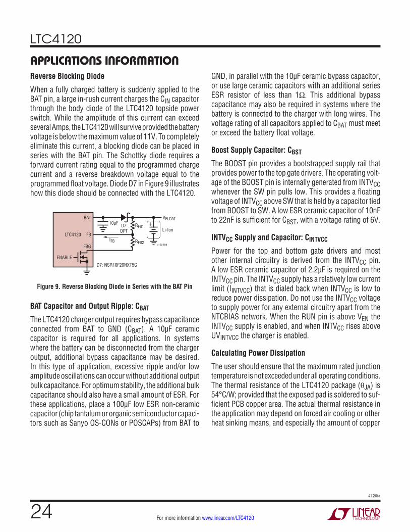
When a fully charged battery is suddenly applied to the BAT pin, a large in-rush current charges the CIN capacitor through the body diode of the LTC4120 topside power switch. While the amplitude of this current can exceed several Amps, the LTC4120 will survive provided the battery voltage is below the maximum value of 11V. To completely eliminate this current, a blocking diode can be placed in series with the BAT pin. The Schottky diode requires a forward current rating equal to the programmed charge current and a reverse breakdown voltage equal to the programmed float voltage. Diode D7 in Figure 9 illustrates how this diode should be connected with the LTC4120.
GND, in parallel with the 10µF ceramic bypass capacitor, or use large ceramic capacitors with an additional series ESR resistor of less than 1Ω. This additional bypass capacitance may also be required in systems where the battery is connected to the charger with long wires. The voltage rating of all capacitors applied to CBAT must meet or exceed the battery float voltage.
Boost Supply Capacitor: CBST
The BOOST pin provides a bootstrapped supply rail that provides power to the top gate drivers. The operating volt-age of the BOOST pin is internally generated from INTVCC whenever the SW pin pulls low. This provides a floating voltage of INTVCC above SW that is held by a capacitor tied from BOOST to SW. A low ESR ceramic capacitor of 10nF to 22nF is sufficient for CBST, with a voltage rating of 6V.
INTVCC Supply and Capacitor: CINTVCC
Power for the top and bottom gate drivers and most other internal circuitry is derived from the INTVCC pin. A low ESR ceramic capacitor of 2.2µF is required on the INTVCC pin. The INTVCC supply has a relatively low current limit (IINTVCC) that is dialed back when INTVCC is low to reduce power dissipation. Do not use the INTVCC voltage to supply power for any external circuitry apart from the NTCBIAS network. When the RUN pin is above VEN the INTVCC supply is enabled, and when INTVCC rises above UVINTVCC the charger is enabled.
Calculating Power Dissipation
The user should ensure that the maximum rated junction temperature is not exceeded under all operating conditions. The thermal resistance of the LTC4120 package (θJA) is 54°C/W; provided that the exposed pad is soldered to suf-ficient PCB copper area. The actual thermal resistance in the application may depend on forced air cooling or other heat sinking means, and especially the amount of copper
BAT10µF RFB1
Li-Ion
VFLOAT
D7OPT
IFB
FB
FBG
LTC4120
ENABLE
+
RFB2
D7: NSR10F20NXT5G
4120 F09
Figure 9. Reverse Blocking Diode in Series with the BAT Pin
BAT Capacitor and Output Ripple: CBAT
The LTC4120 charger output requires bypass capacitance connected from BAT to GND (CBAT). A 10µF ceramic capacitor is required for all applications. In systems where the battery can be disconnected from the charger output, additional bypass capacitance may be desired. In this type of application, excessive ripple and/or low amplitude oscillations can occur without additional output bulk capacitance. For optimum stability, the additional bulk capacitance should also have a small amount of ESR. For these applications, place a 100µF low ESR non-ceramic capacitor (chip tantalum or organic semiconductor capaci-tors such as Sanyo OS-CONs or POSCAPs) from BAT to

LTC4120
254120fa
For more information www.linear.com/LTC4120
applicaTions inForMaTionon the PCB to which the LTC4120 is attached. The actual power dissipation while charging is approximated by the following formula:
PD ≅ VIN – VBAT( ) • ITRKL
+VIN • IIN(SWITCHING)
+RSNS • ICHG2
+RDS(ON)(TOP) •VBATVIN
• ICHG2
+RDS(ON)(BOT) • 1–VBATVIN
⎛
⎝⎜⎞
⎠⎟• ICHG2
During trickle charge (VBAT < VTRKL) the power dissipation may be significant as ITRKL is typically 10mA, however during normal charging the ITRKL term is zero.
The junction temperature can be estimated using the fol-lowing formula:
TJ = TA + PD • θJA
where TA is the ambient operating temperature.
Significant power is also consumed in the transmitter electronics. The large AC voltage generated across the LX and CX tank results in power being dissipated in the DC resistance of the LX coil and the ESR of the CX capacitor. The large induced magnetic field in the LX coil may also induce heating in nearby metallic objects.
PCB Layout
To prevent magnetic and electrical field radiation and high frequency resonant problems, proper layout of the components connected to the LTC4120 is essential. For maximum efficiency, the switch node rise and fall times should be minimized. The following PCB design priority list will help insure proper topology. Layout the PCB using the guidelines listed below in this specific order.
1. Keep foreign metallic objects away from the transmit-ter coil. Metallic objects in proximity to the transmit coil will suffer from induction heating and will be a source of power loss. With the exception of a ferrite shield that can be used to improve the coupling from transmitter coil to receiver coil when placed behind the transmitter coil.
Advanced transmitters from PowerByProxi include features to detect the presence of foreign metallic objects that mitigates this issue.
2. VIN input capacitor should be placed as close as pos-sible to the IN and GND pins, with the shortest copper traces possible and a via connection to the GND plane
3. Place the switching inductor as close as possible to the SW pin. Minimize the surface area of the SW pin node. Make the trace width the minimum needed to support the programmed charge current, and ensure that the spacing to other copper traces be maximized to reduce capacitance from the SW node to any other node.
4. Place the BAT capacitor adjacent to the BAT pin and ensure that the ground return feeds to the same cop-per that connects to the input capacitor ground before connecting back to system ground.
5. Route analog ground (RUN ground and INTVCC capaci-tor ground) as a separate trace back to the LTC4120 GND pin before connecting to any other ground.
6. Place the INTVCC capacitor as close as possible to the INTVCC pin with a via connection to the GND plane.
7. Route the DHC trace with sufficient copper and vias to support 350mA of RMS current, and ensure that the spacing from the DHC node to other copper traces be maximized to reduce capacitance and radiated EMI from the DHC node to other sensitive nodes.
8. It is important to minimize parasitic capacitance on the PROG pin. The trace connecting to this pin should be as short as possible with extra wide spacing from adjacent copper traces.
9. Minimize capacitive coupling to GND from the FB pin.
10. Maximize the copper area connected to the exposed pad. Place via connections directly under the exposed pad to connect a large copper ground plane to the LTC4120 to improve heat transfer.
applicaTions inForMaTion
LTC4120
264120fa
For more information www.linear.com/LTC4120
applicaTions inForMaTionDesign Examples
The design example illustrated in Figure 10, reviews the design of the resonant coupled power transfer charger application. First the design of the wireless power receiver circuit is described. Then consider the design for the charger function given the maximum input voltage, a battery float voltage of 8.2V, and a charge current of 200mA for the LTC4120. This example also demonstrates how to select the switching inductance value to avoid discontinuous conduction; where switching noise increases.
The wireless power receiver is formed by the tuned net-work LR and C2P, C2S. This tuned network automatically modulates the resonance of the tank with the DHC pin of the LTC4120 to optimize power transfer. The resonant frequency of the tank should match the oscillation fre-quency of the transmitter. Given the transmitter shown in Figure 3 this frequency is 130kHz. The tuned receiver resonant frequency is:
fT =
12 • π • LR • (C2P + C2S)
= 131kHz
In this design example, the de-tuned resonant frequency is:
fD =
12 • π • LR • C2S
= 142kHz
fD should be set between 5% and 15% higher than fT. A higher level gives more control range but results in more power dissipation.
A 47µH coil is selected for LR to obtain a turns ratio of 3:1 from the transmitter coil, LX = 5µH.
Now C2S can be calculated to be 26.7nF. Two standard parallel 50V rated capacitors, 22nF and 4.7nF, provide a value within 1% of the calculated C2S. Now C2P can be calculated to be 6.5nF which can be obtained with 4.7nF and 1.8nF capacitors in parallel. All of the capacitors should be selected with 5% or better tolerance.
The rectifier, D8, D9 and D5 are selected as 50V rated Schottky diodes.
Now consider the design circuit for the LTC4120 charger function. First, the external feedback divider, RFB1/RFB2, is found using standard 0.1% values:
RFB1 =8.2V • 588k
2.5V≅ 1.93M
RFB2 =1.96M • 588k1.96M – 588k
≅ 845k
With these resistors, and including the resistance of the FBG pin, the battery float voltage is 8.204V.
With an 8.2V float voltage the maximum charge current available is limited by the maximum power available from the RCPT at ηEFF = 85% charger efficiency:
ICHG(MAX) ≤
85% • 2W8.2V
= 207mA
A charge current of 200mA is achieved by selecting a standard 1% RPROG resistor of:
RPROG =
hPROG • VPROGICHG
= 6.04k
While charging a battery, the resonant receiver is loaded by the charge current, this load reduces the input voltage from the open-circuit value to a typical voltage in a range from 12V (at UVCL) up to about 26V. The amplitude of this voltage depends primarily on the amount of coupling between the transmitter and the receiver, typically this voltage is about 17V.
The maximum loaded input voltage is used to select the operating frequency and influences the value of the switch-ing inductor. The saturation current rating of the switching inductor is selected based on the worst case conditions at the maximum open-circuit voltage.
A typical 2-cell Li-Ion battery pack engages pack protection for VBAT less than 5V, this is the lowest voltage considered for determining the on-time and selecting the 1.35MHz operating frequency.
tON =
5V1.35MHz • 17V
= 349ns > tMIN(ON)
applicaTions inForMaTion

LTC4120
274120fa
For more information www.linear.com/LTC4120
applicaTions inForMaTionNow the switching inductor value is calculated. The induc-tor value is calculated based on achieving a 30% ripple current. The ripple current is calculated at the typical input operating voltage of 17V:
L3 >
17V – 8.2V( ) • 8.2V2 • 1.35MHz • 17V • 30% • 200mA( )
= 27µH
33µH is the next standard inductor value that is greater than this minimum. This inductor value results in a worst-case ripple current at the input open-circuit voltage, VIN(OC).VIN(OC) is estimated based on the transmitter design in Figure 3, at the largest coupling coefficient k = 0.37 as:
VIN(OC) = k • n • π • VIN(TX)
VIN(OC) = 0.37 • 3 • 3.14 • 5V = 34.9V
∆IL =
34.9V – 8.2V( ) • 8.2V1.35MHz • 33µH • 34.9V
= 141mA
This results in a worst-case peak inductor current of:
IL(PEAK) = ICHG +
∆IL2
= 271mA
Select an inductor with a saturation current rating greater than the worst-case peak inductor current of 271mA.
Select a 50V rated capacitor for CIN = 10µF to achieve an input voltage ripple of 10mV at the typical operating input voltage of 17V:
∆VIN =
200mA • 8.2V17V
10µF= 10mV
And select 6V rated capacitors for CINTVCC = 2.2µF, CBOOST = 22nF, and CBAT = 10µF. Optionally add diode D6, a 1W, 39V Zener diode if the coupling from transmitter to receiver coils is not well enough controlled to ensure that VIN remains below 39V when the battery is fully charged.
Finally the RUN pin divider is selected to turn on the char-ger once the input voltage reaches 11.2V. With R3 = 374k and R4 = 102k the RUN pin reaches 2.4V at VIN = 11.2V. With this RUN pin divider, the LTC4120 is disabled once VIN falls below 10.5V.
For this design example, power dissipation during trickle charge, where the switching charge current is 20mA and the linear charge current is 10mA is calculated as follows:
PD = 20V – 5V( ) • 10mA
+20V • 3.2mA
+0.2Ω • 0.02A2
+0.7Ω •5V
20V• 0.02A2
+0.35Ω • 1–5V
20V⎛⎝⎜
⎞⎠⎟
• 0.02A2
= 0.21W
This dissipated power results in a junction temperature rise of:
PD • θJA = 0.2W • 54°C/W = 11°C
During regular charging with VBAT > VTRKL, the power dissipation reduces to:
PD = 20V • 3.2mA
+0.2Ω • 0.2A2
+0.7Ω •8.2V20V
• 0.2A2
+0.35Ω • 1–8.2V20V
⎛⎝⎜
⎞⎠⎟
• 0.2A2
= 92mW
This dissipated power results in a junction temperature rise of 5°C over ambient.

LTC4120
284120fa
For more information www.linear.com/LTC4120
package DescripTionPlease refer to http://www.linear.com/designtools/packaging/ for the most recent package drawings.
3.00 ±0.10(4 SIDES)
RECOMMENDED SOLDER PAD PITCH AND DIMENSIONS
1.45 ±0.05(4 SIDES)
NOTE:1. DRAWING CONFORMS TO JEDEC PACKAGE OUTLINE MO-220 VARIATION (WEED-2)2. DRAWING NOT TO SCALE3. ALL DIMENSIONS ARE IN MILLIMETERS4. DIMENSIONS OF EXPOSED PAD ON BOTTOM OF PACKAGE DO NOT INCLUDE MOLD FLASH. MOLD FLASH, IF PRESENT, SHALL NOT EXCEED 0.15mm ON ANY SIDE5. EXPOSED PAD SHALL BE SOLDER PLATED6. SHADED AREA IS ONLY A REFERENCE FOR PIN 1 LOCATION ON THE TOP AND BOTTOM OF PACKAGE
PIN 1TOP MARK(NOTE 6)
0.40 ±0.10
BOTTOM VIEW—EXPOSED PAD
1.45 ± 0.10(4-SIDES)
0.75 ±0.05 R = 0.115TYP
0.25 ±0.05
1
PIN 1 NOTCH R = 0.20 TYPOR 0.25 × 45° CHAMFER
15 16
2
0.50 BSC
0.200 REF
2.10 ±0.053.50 ±0.05
0.70 ±0.05
0.00 – 0.05
(UD16) QFN 0904
0.25 ±0.050.50 BSC
PACKAGE OUTLINE
UD Package16-Lead Plastic QFN (3mm × 3mm)
(Reference LTC DWG # 05-08-1691 Rev Ø)

LTC4120
294120fa
For more information www.linear.com/LTC4120
Information furnished by Linear Technology Corporation is believed to be accurate and reliable. However, no responsibility is assumed for its use. Linear Technology Corporation makes no representa-tion that the interconnection of its circuits as described herein will not infringe on existing patent rights.
revision hisToryREV DATE DESCRIPTION PAGE NUMBER
A 12/13 Updated Table 4 component values and brands. 20

LTC4120
304120fa
For more information www.linear.com/LTC4120 LINEAR TECHNOLOGY CORPORATION 2013
LT 1213 • PRINTED IN USALinear Technology Corporation1630 McCarthy Blvd., Milpitas, CA 95035-7417(408) 432-1900 ● FAX: (408) 434-0507 ● www.linear.com/LTC4120
relaTeD parTs
Typical applicaTion
PART NUMBER DESCRIPTION COMMENTS
LT3650-8.2/LT3650-8.4
Monolithic 2A Switch Mode Non-Synchronous 2-Cell Li-Ion Battery Charger
Standalone 9V ≤ VIN ≤ 32V (40V Absolute Maximum), 1MHz, 2A Programmable Charge Current, Timer or C/10 Termination, Small and Few External Components, 3mm × 3mm DFN-12 Package “-8.2” for 2× 4.1V Float Voltage Batteries, “-8.4” for 2× 4.2V Float Voltage Batteries
LT3650-4.1/LT3650-4.2
Monolithic 2A Switch Mode Non-Synchronous 1-Cell Li-Ion Battery Charger
Standalone 4.75V ≤ VIN ≤ 32V (40V Absolute Maximum), 1MHz, 2A Programmable Charge Current, Timer or C/10 Termination, Small and Few External Components, 3mm × 3mm DFN-12 Package “-4.1” for 4.1V Float Voltage Batteries, “-4.2” for 4.2V Float Voltage Batteries
LT3652HV Power Tracking 2A Battery Charger
Input Supply Voltage Regulation Loop for Peak Power Tracking in (MPPT) Solar Applications Standalone, 4.95V ≤ VIN ≤ 34V (40V Absolute Maximum), 1MHz, 2A Charge Current, 3.3V ≤ VOUT ≤ 18V. Timer or C/10 Termination, 3mm × 3mm DFN-12 Package and MSOP-12 Packages
LTC4070 Li-Ion/Polymer Shunt Battery Charger System
Low Operating Current (450nA), 1% Float Voltage Accuracy Over Full Temperature and Shunt Current Range, 50mA Maximum Internal Shunt Current (500mA with External PFET), Pin Selectable Float Voltages: 4.0V, 4.1V, 4.2V. Ultralow Power Pulsed NTC Float Conditioning for Li-Ion/Polymer Protection, 8-Lead (2mm × 3mm) DFN and MSOP
LTC4071 Li-Ion/Polymer Shunt Battery Charger System with Low Battery Disconnect
Integrated Pack Protection, <10nA Low Battery Disconnect Protects Battery From Over-Discharge. Low Operating Current (550nA), 1% Float Voltage Accuracy Over Full Temperature and Shunt Current Range, 50mA Maximum Internal Shunt Current, Pin Selectable Float Voltages: 4.0V, 4.1V, 4.2V. Ultralow Power Pulsed NTC Float Conditioning for Li-Ion/Polymer Protection, 8-Lead (2mm × 3mm) DFN and MSOP
LTC4065/LTC4065A
Standalone Li-Ion Battery Charger in 2mm × 2mm DFN
4.2V ±0.6% Float Voltage, Up to 750mA Charge Current ; “A” Version Has /ACPR Function. 2mm × 2mm DFN Package
Figure 10. Resonant Coupled Power Transfer Charger Application
INTVCCIN
RUN
FREQ
CHRG
FAULT
2kBOOST
SW
CHGSNS
DHC
RPROG6.04k
4120 F10
Li-IonT
CBST22nF
C2S26.7nF
C2P6.5nF
LR47µH
LX5µH
CIN10µFD8 D5 D6
OPT
D9
CINTVCC2.2µF
CBAT10µF
VFLOAT8.2V
LSW47µH
NTCPROG
LTC4120
GND
BAT
FB
FBG
RFB11.93M
RFB2845k
10k
+
2k
374k
102k
D5, D8, D9: DFLS240LD6: MMSZ5259BT1G OR DFLZ39 (OPT)LSW: SLF6028-470MR59T: NTHS0402N02N1002F
Tx CIRCUITRY