wireless charging - some key elements
TRANSCRIPT
Wireless Charging - some key elements
Eva Palmberg, Sonja Lundmark, Mikael Alatalo, Torbjorn Thiringerand Robert Karlsson
Department of Energy and Environment
CHALMERS UNIVERSITY OF TECHNOLOGY
Goteborg, Sweden 2013

2
Wireless Charging - some key elements
EVA PALMBERG, SONJA LUNDMARK, MIKAEL ALATALO, TORBJORN THIRINGER AND ROBERT KARLSSON
Department of Energy and EnvironmentCHALMERS UNIVERSITY OF TECHNOLOGY
Goteborg, Sweden 2013
3
Wireless Charging - some key elements
Eva Palmberg, Sonja Lundmark, Mikael Alatalo, Torbjorn Thiringer and Robert Karlsson
Printed in Sweden Goteborg 2013
c©Eva Palmberg, Sonja Lundmark, Mikael Alatalo, Torbjorn Thiringer and Robert Karlsson
Technical report 2013:1Department of Energy and EnvironmentDivision of Electric Power Engineering
CHALMERS UNIVERSITY OF TECHNOLOGY
SE-412 96 Goteborg
Sweden
4

Abstract
In this report so called wireless charging is investigated. The base concept investigated is asending coil and a receiving coil at various heights, mainly using air, but also assisted withferrites. Both analytical expressions a well as FEM analyses have been conducted. RegardingFEM analyses 2D as well as 3D analyses have been performed. Maxwell as well as ComsolMultiphysics have been utilised as FEM software.
The theory behind wireless energy transfer is presented and the dependencies of variousgeometrical parameters are established. The needed components for a wireless charging unitis described and analyzed, showing how design aspects (such as number of turns),frequencies, height and vertical displacement affect the results. Finally comparisons towardsexperiments have been done.
It is found that less sensitivity towards displacements can be achieved if the coils of thereceiving coil are placed next to each other (instead of placing the coils as one inner ring coilinside an outer ring coil), and by increasing the air gap between a receiving and a sendingcoil. It is also shown that it is efficient to use ferrite plates adjacent to the coils in order to getmore power to the load and to avoid high magnetic fields outside the charging system. It isalso shown that coils (sending and/or receiving) with several conductors should have theouter conductor distanced from the inner ones as this will reduce skin effect, and thereforereduces the coil resistance.
The relatively long air gap of the wireless charging unit has some implications. There will behigh leakage and a lot of flux will penetrate the winding, resulting in high losses at highfrequencies. The thin conductors of a Litz-wire make it possible to lessen the eddy currentsand skin effect in the conductors. It was further found that the efficiency of a 100 kWcharging system was approximately 94 %.
Regarding comparisons between experiments and analytical expressions, it is found that theaccuracy of the FEM model is especially important for the calculation of the resistance at highfrequencies. The comparison between FEM programs and analytical calculations showed asmall discrepancy. When comparing with measurements the discrepancy was larger. Thiscould be explained with the complicated geometry of the coils.
5

6
Acknowledgement
The authors would like to thank the 3rd year students at the school of Electrical Engineering2010, 2011 and 2012 that have been constructing experimental equipment that has been usedin this report.
Thanks also to Raquel Montalvo, who also conducted experiments that have been useful forthis work.
The financial support given by Goteborg Energi AB is gratefully acknowledged.
7

8
Contents
Abstract 5
Acknowledgement 7
1 Introduction 11
2 Wireless transfer basics 132.1 Geometry dependence of the mutual inductance M at low frequencies, 2D . . . 13
2.1.1 Changing the geometry . . . . . . . . . . . . . . . . . . . . . . . . . . . . 142.1.2 Geometry dependence of M using ferrites . . . . . . . . . . . . . . . . . . 182.1.3 Coupling factors . . . . . . . . . . . . . . . . . . . . . . . . . . . . . . . . 232.1.4 Frequency dependence . . . . . . . . . . . . . . . . . . . . . . . . . . . . 24
2.2 Calculation of the parameters in a cylindrical 3D model . . . . . . . . . . . . . . 242.2.1 Current densities and losses in the wires . . . . . . . . . . . . . . . . . . 262.2.2 Parameters . . . . . . . . . . . . . . . . . . . . . . . . . . . . . . . . . . . . 272.2.3 Comparison of models . . . . . . . . . . . . . . . . . . . . . . . . . . . . . 27
2.3 Resonant coupling . . . . . . . . . . . . . . . . . . . . . . . . . . . . . . . . . . . 282.4 Conclusions of Chapter 2 . . . . . . . . . . . . . . . . . . . . . . . . . . . . . . . . 29
3 Modelling the wireless transfer coil system into Ansys 313.1 Verification against analytical problems . . . . . . . . . . . . . . . . . . . . . . . 32
3.1.1 One long coil . . . . . . . . . . . . . . . . . . . . . . . . . . . . . . . . . . 333.1.2 One ring coil . . . . . . . . . . . . . . . . . . . . . . . . . . . . . . . . . . . 343.1.3 Two ring coils . . . . . . . . . . . . . . . . . . . . . . . . . . . . . . . . . . 35
3.2 Comparison to a master thesis work; two ring coils with Ferrite and Al-plates . 363.3 Comparison to a bachelor thesis work; a flat helix coil with 3 turns . . . . . . . 38
3.3.1 2D axisymmetric transient model of a flat circular coil with 3 turns . . . 393.3.2 A 3D transient model of a flat circular coil with 3 separate turns . . . . 413.3.3 A 3D transient model of a flat helix coil with 3 circular turns . . . . . . . 433.3.4 A 3D transient model of a flat helix coil with 3 rectangular turns . . . . . 453.3.5 A 3D eddy current model of a flat helix coil, finer mesh . . . . . . . . . . 473.3.6 Comparison to a bachelor thesis work; two frequencies . . . . . . . . . . 47
3.4 Conclusions of Chapter 3 . . . . . . . . . . . . . . . . . . . . . . . . . . . . . . . 49
4 Wireless charger unit 514.1 Overview of charger . . . . . . . . . . . . . . . . . . . . . . . . . . . . . . . . . . 514.2 Transformer . . . . . . . . . . . . . . . . . . . . . . . . . . . . . . . . . . . . . . . 524.3 Power Electronics . . . . . . . . . . . . . . . . . . . . . . . . . . . . . . . . . . . . 584.4 Resonant circuit . . . . . . . . . . . . . . . . . . . . . . . . . . . . . . . . . . . . . 594.5 Control of transformer current . . . . . . . . . . . . . . . . . . . . . . . . . . . . 604.6 Model and simulation results . . . . . . . . . . . . . . . . . . . . . . . . . . . . . 614.7 Alternative system . . . . . . . . . . . . . . . . . . . . . . . . . . . . . . . . . . . 644.8 Conclusions of Chapter 4 . . . . . . . . . . . . . . . . . . . . . . . . . . . . . . . . 66
5 Conclusions 67
9

10
Chapter 1
Introduction
Today (2012) we are in the beginning of the installations of charger stations for electrifiedvehicles. So far the charging is made using ’conductive’ techniques, i.e. that there is a directelectrical contact between charger and the vehicle, dominating is the concept of having acable that is plugged in using some type of connector.
In order to make the charging more convenient, it would be very good if it could be moreautomated. Of course this can be done using the ’conductive technique’, but more suitablewould be to use the inductive principle where energy is transmitted from a sending coil to areceiving coil in the vehicles, so called ’inductive charging’ or ’wireless charging’.
At the division of Electric Power Engineering at Chalmers University of Technology, aplug-in gokart is a subject of project for the students following the electrical engineeringcurriculum. In this, wireless charging is a theme where the students in projects do small stepsin order to enhance the electrification in the plug-in gokart.
In order to develop this technique more knowledge about wireless charging is needed. Bothfundamental theories as well as calculation methods needs to be enhanced and this has beenmade possible through the grant from Goteborg Energi that was awarded for this activity.
In order to summarize the wireless activities at the division of electric power engineering,this report has been written with the objective to
• Present the theory behind wireless energy transfer and establish the dependencies ofvarious geometrical parameters.
• Compare various calculation complexities to establish the needs of deepness in themodelling.
• Describe the needed components for a wireless charging unit and for exampledetermine the losses in the various parts.
• Determine how design aspects (such as number of turns), frequencies, height andvertical displacement affect the results.
• To verify some parts experimentally.
11

12
Chapter 2
Wireless transfer basics
2.1 Geometry dependence of the mutual inductance
M at low frequencies, 2D
Let us study two rectangular loops in air, length 1 m in the z-direction, width 1 m each in thex-direction, see Figure 2.1. A current i1 flows in the lower (sending) loop. The inducedvoltage in the upper (pick-up) loop will be vind2
=Mdi1/dt. How will the mutual inductanceM be changed when changing the geometry? The number of turns, N1 and N2, the frequencyand the currents in the loops will not be chosen yet.
h
x
x1
⊗ i1
⇑Φ12
⊙i1
1 m
Figure 2.1: Two rectangular loops with current in the lower one.The upper loop is the pick-up loop. Unit length in the z-direction.
The flux through the pick-up loop is caused by the current i1 and M=N2Φ12/i1. The flux canbe written as Φ12 =
∫
SB12 · ds =
∮
A12 · dl2 = Az(left)−Az(right), where A12 is the magneticvector potential at the circumference of loop 2 caused by i1. Maximum flux through loop 2,that is maximum M, will thus be for the difference in vector potentials being maximum. Orrather Az(left)-Az(right) being maximal.
a/ Analytical calculations of the parameters for a loop, width d=1m, 1 m in the lengthdirection, one turn and radius of the wire a= 5·10−3 m, will give the self inductance L, asshown in equation 2.1.
L =µ0
π
[1
4+ ln
d
a
]
(2.1)
Dividing L into two parts Louter = 2.11 µH/m and Linner = 0.1 µH/m. - Linner =µ0
4πis the
inductance arisen from the magnetic fields inside the conductors. - For low frequenciesLtot = 2.21µH/m. For very high frequencies Linner =0. The resistance R= 0.439 mΩ/m for lowfrequencies. When the frequency is chosen, we can calculate Ltot and the resistance R.
The calculation of the mutual inductance M will give the expression shown in equation 2.2 .
M =µ0
2πln
r2r3r1r4
(2.2)
where r1 =√
h2 + x21, r2 =√
h2 + (x1 + d2)2, r3 =√
h2 + (d1 − x1)2 and
r4 =√
h2 + (x1 + d2 − d1)2 Assuming two equal loops d1 = d2 = d = 1 m.
For x1=0 and h= 0.1 m we get M = 0.92 µH/m. For x1=0.1 and h=0.1 m we get M = 0.78µH/m.
b/ A simulation in Comsol’s Multiphysics for i1 = 1A in the sending loop will give the B-lines(A=const) according to Figure 2.2. The reference for the vector potential A=0 is set on the linex=0.5. A>0 for x<0.5 m and A<0 for x>0.5 m. The pick-up loop must have one side to theleft and the other side to the right so that Az(left)-Az(right) will add for maximum M. Thevector potential is high close to the current loop.
13
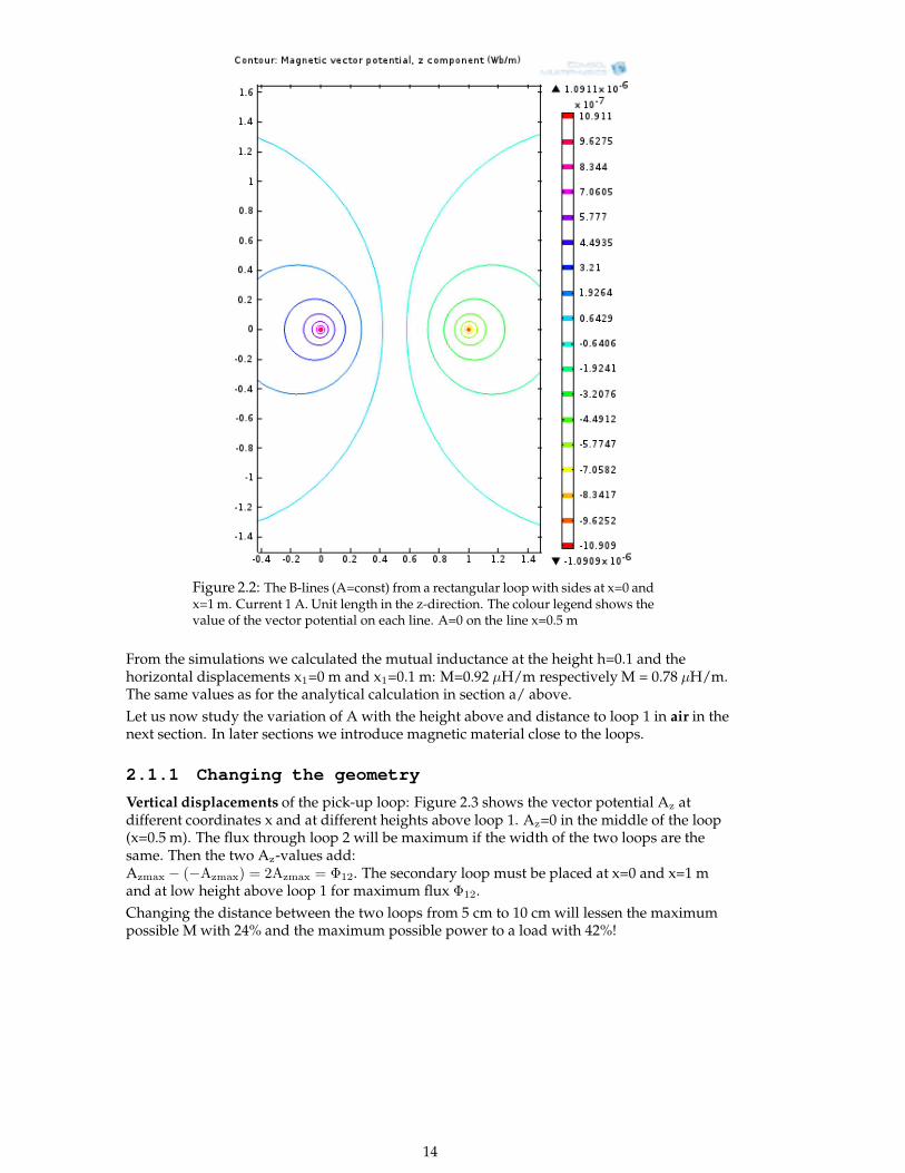
Figure 2.2: The B-lines (A=const) from a rectangular loop with sides at x=0 andx=1 m. Current 1 A. Unit length in the z-direction. The colour legend shows thevalue of the vector potential on each line. A=0 on the line x=0.5 m
From the simulations we calculated the mutual inductance at the height h=0.1 and thehorizontal displacements x1=0 m and x1=0.1 m: M=0.92 µH/m respectively M = 0.78 µH/m.The same values as for the analytical calculation in section a/ above.
Let us now study the variation of A with the height above and distance to loop 1 in air in thenext section. In later sections we introduce magnetic material close to the loops.
2.1.1 Changing the geometry
Vertical displacements of the pick-up loop: Figure 2.3 shows the vector potential Az atdifferent coordinates x and at different heights above loop 1. Az=0 in the middle of the loop(x=0.5 m). The flux through loop 2 will be maximum if the width of the two loops are thesame. Then the two Az-values add:Azmax − (−Azmax) = 2Azmax = Φ12. The secondary loop must be placed at x=0 and x=1 mand at low height above loop 1 for maximum flux Φ12.
Changing the distance between the two loops from 5 cm to 10 cm will lessen the maximumpossible M with 24% and the maximum possible power to a load with 42%!
14
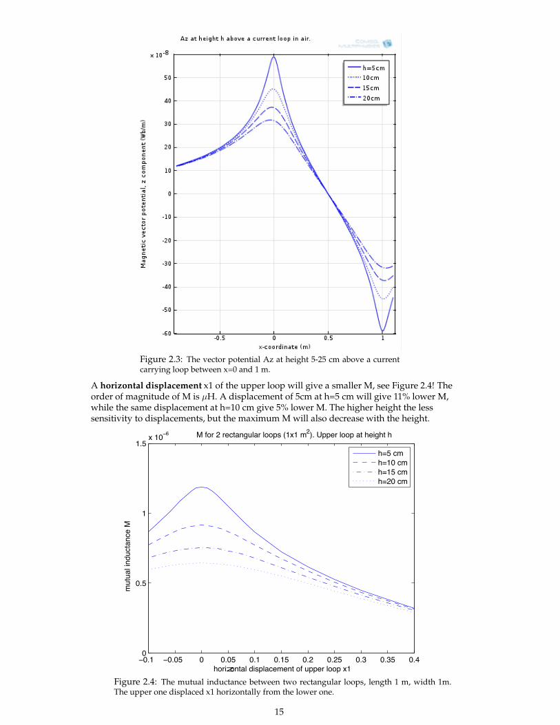
Figure 2.3: The vector potential Az at height 5-25 cm above a currentcarrying loop between x=0 and 1 m.
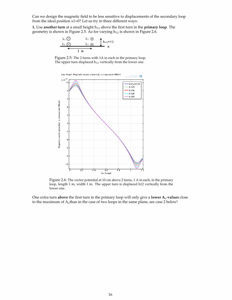
A horizontal displacement x1 of the upper loop will give a smaller M, see Figure 2.4! Theorder of magnitude of M is µH. A displacement of 5cm at h=5 cm will give 11% lower M,while the same displacement at h=10 cm give 5% lower M. The higher height the lesssensitivity to displacements, but the maximum M will also decrease with the height.
!!"# !!"!$ ! !"!$ !"# !"#$ !"% !"%$ !"& !"&$ !"'!
!"$
#
#"$()#!
!*
)+,-./,0123)4.5632789801),:);668-)3,,6)(#
9;1;23).04;712078)<))=µ>
)))))))))))))<):,-)%)-87120?;32-)3,,65)=#(#)9%@")A668-)3,,6)21)+8.?+1)+))
)
)
+B$)79
+B#!)79
+B#$)79
+B%!)79
Figure 2.4: The mutual inductance between two rectangular loops, length 1 m, width 1m.The upper one displaced x1 horizontally from the lower one.
15
Can we design the magnetic field to be less sensitive to displacements of the secondary loopfrom the ideal position x1=0? Let us try in three different ways:
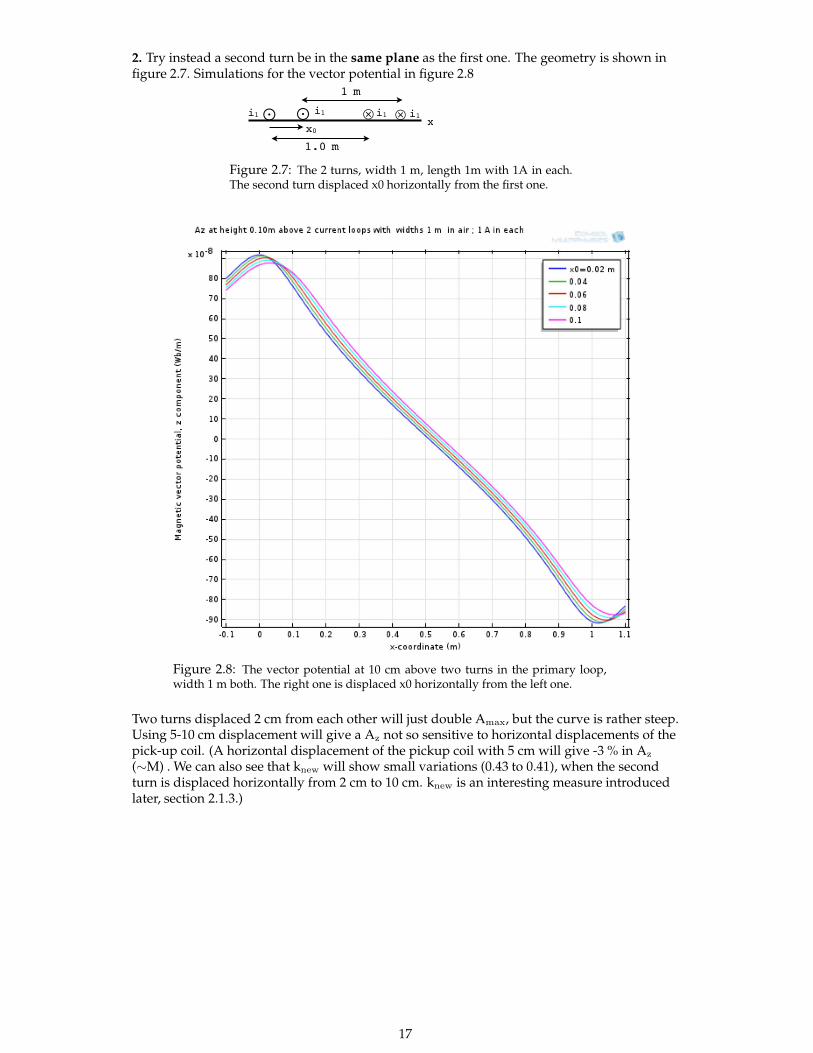
1. Use another turn at a small height h12 above the first turn in the primary loop. Thegeometry is shown in Figure 2.5. Az for varying h12 is shown in Figure 2.6.
h12<<1
x⊗i1⊙i1
1 m
⊙ ⊗i1i1
Figure 2.5: The 2 turns with 1A in each in the primary loop.The upper turn displaced h12 vertically from the lower one.
Figure 2.6: The vector potential at 10 cm above 2 turns, 1 A in each, in the primaryloop, length 1 m, width 1 m. The upper turn is displaced h12 vertically from thelower one.
One extra turn above the first turn in the primary loop will only give a lower Az-values closeto the maximum of Azthan in the case of two loops in the same plane, see case 2 below!
16
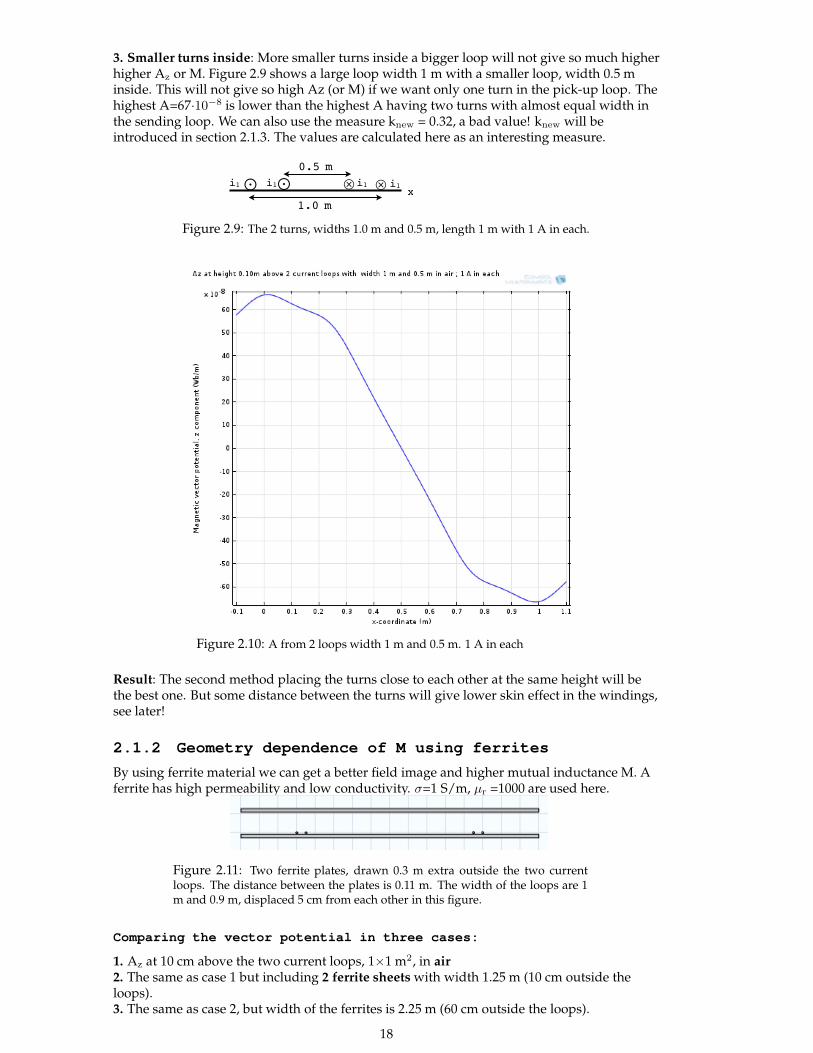
2. Try instead a second turn be in the same plane as the first one. The geometry is shown infigure 2.7. Simulations for the vector potential in figure 2.8
xi1⊙i1
1.0 m
⊙ ⊗ i1i1 ⊗
1 m
x0
Figure 2.7: The 2 turns, width 1 m, length 1m with 1A in each.The second turn displaced x0 horizontally from the first one.
Figure 2.8: The vector potential at 10 cm above two turns in the primary loop,width 1 m both. The right one is displaced x0 horizontally from the left one.
Two turns displaced 2 cm from each other will just double Amax, but the curve is rather steep.Using 5-10 cm displacement will give a Az not so sensitive to horizontal displacements of thepick-up coil. (A horizontal displacement of the pickup coil with 5 cm will give -3 % in Az
(∼M) . We can also see that knew will show small variations (0.43 to 0.41), when the secondturn is displaced horizontally from 2 cm to 10 cm. knew is an interesting measure introducedlater, section 2.1.3.)
17
3. Smaller turns inside: More smaller turns inside a bigger loop will not give so much higherhigher Az or M. Figure 2.9 shows a large loop width 1 m with a smaller loop, width 0.5 minside. This will not give so high Az (or M) if we want only one turn in the pick-up loop. Thehighest A=67·10−8 is lower than the highest A having two turns with almost equal width inthe sending loop. We can also use the measure knew = 0.32, a bad value! knew will beintroduced in section 2.1.3. The values are calculated here as an interesting measure.
xi1⊙i1
1.0 m
⊙ ⊗ i1i1 ⊗
0.5 m
Figure 2.9: The 2 turns, widths 1.0 m and 0.5 m, length 1 m with 1 A in each.
Figure 2.10: A from 2 loops width 1 m and 0.5 m. 1 A in each
Result: The second method placing the turns close to each other at the same height will bethe best one. But some distance between the turns will give lower skin effect in the windings,see later!
2.1.2 Geometry dependence of M using ferrites
By using ferrite material we can get a better field image and higher mutual inductance M. Aferrite has high permeability and low conductivity. σ=1 S/m, µr =1000 are used here.
Figure 2.11: Two ferrite plates, drawn 0.3 m extra outside the two currentloops. The distance between the plates is 0.11 m. The width of the loops are 1m and 0.9 m, displaced 5 cm from each other in this figure.
Comparing the vector potential in three cases:
1. Az at 10 cm above the two current loops, 1×1 m2, in air2. The same as case 1 but including 2 ferrite sheets with width 1.25 m (10 cm outside theloops).3. The same as case 2, but width of the ferrites is 2.25 m (60 cm outside the loops).
18
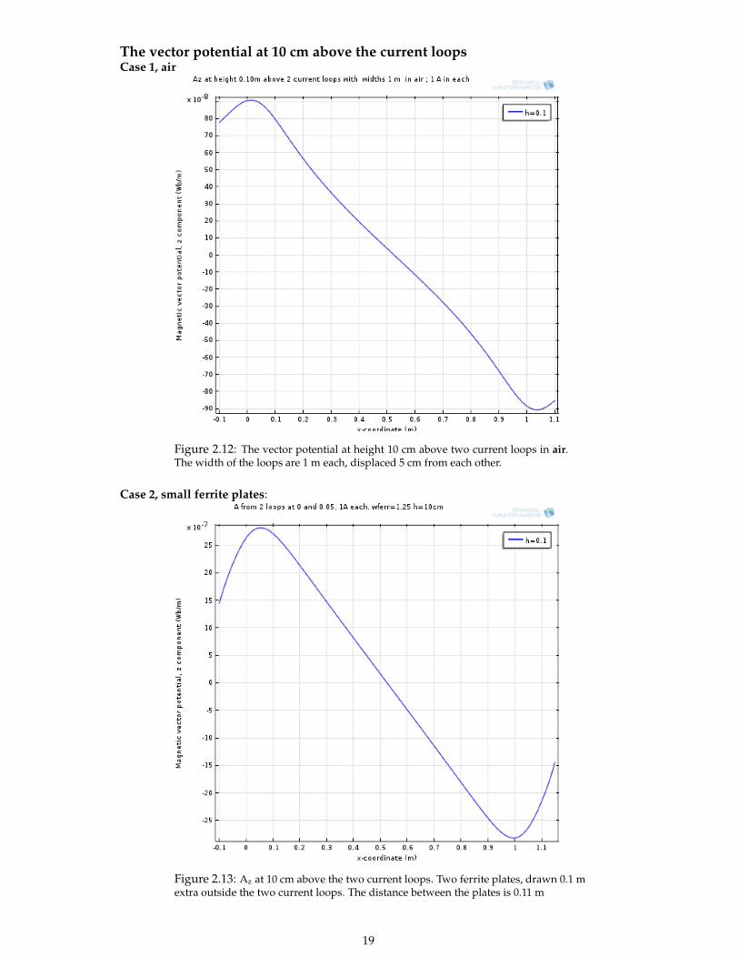
The vector potential at 10 cm above the current loopsCase 1, air
Figure 2.12: The vector potential at height 10 cm above two current loops in air.The width of the loops are 1 m each, displaced 5 cm from each other.
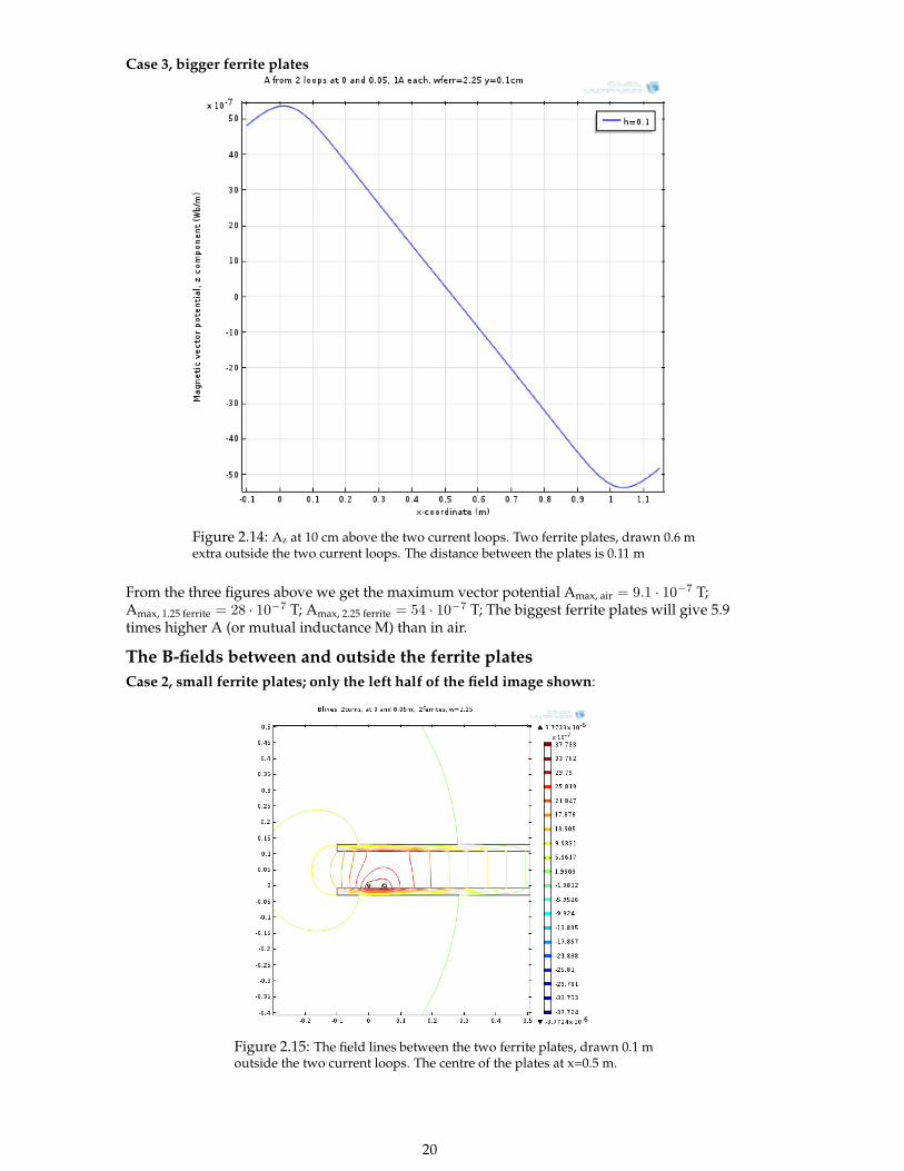
Case 2, small ferrite plates:
Figure 2.13: Az at 10 cm above the two current loops. Two ferrite plates, drawn 0.1 mextra outside the two current loops. The distance between the plates is 0.11 m
19
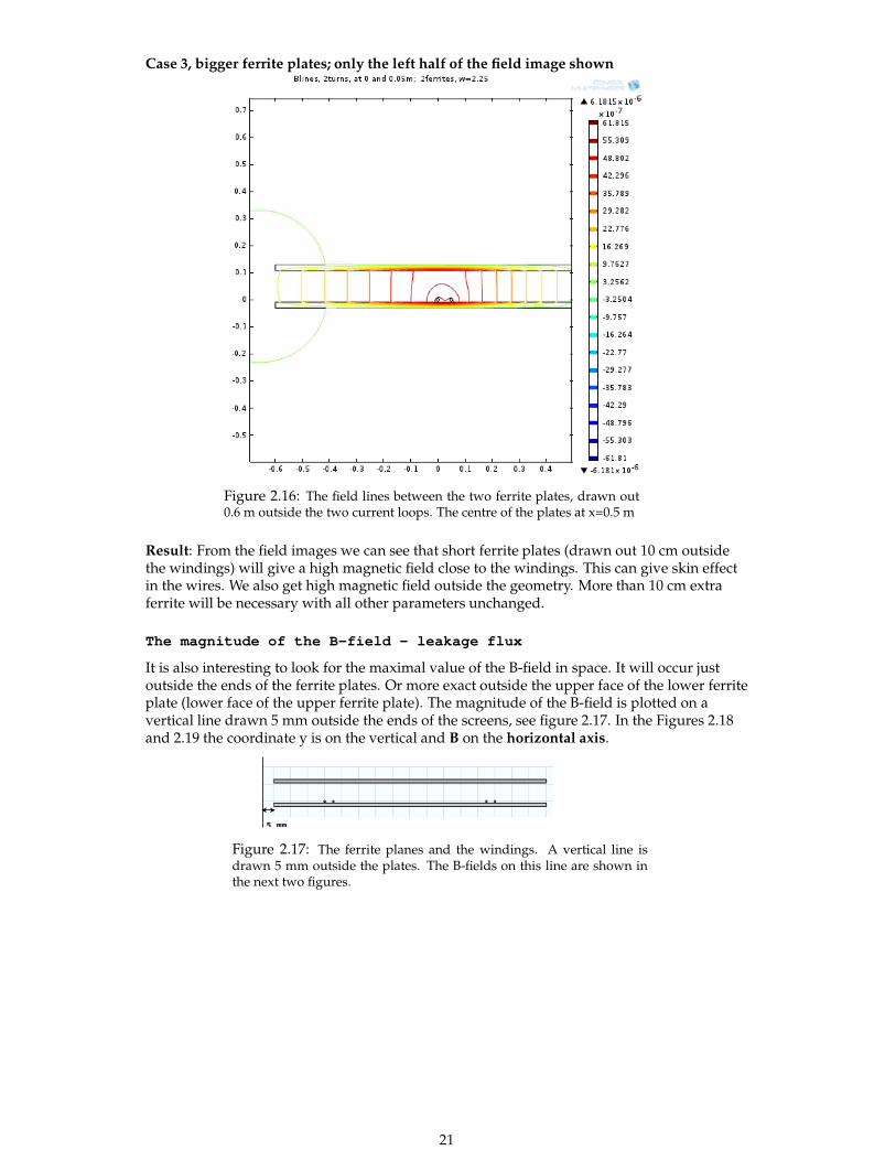
Case 3, bigger ferrite plates
Figure 2.14: Az at 10 cm above the two current loops. Two ferrite plates, drawn 0.6 mextra outside the two current loops. The distance between the plates is 0.11 m
From the three figures above we get the maximum vector potential Amax, air = 9.1 · 10−7 T;Amax, 1.25 ferrite = 28 · 10−7 T; Amax, 2.25 ferrite = 54 · 10−7 T; The biggest ferrite plates will give 5.9times higher A (or mutual inductance M) than in air.
The B-fields between and outside the ferrite plates
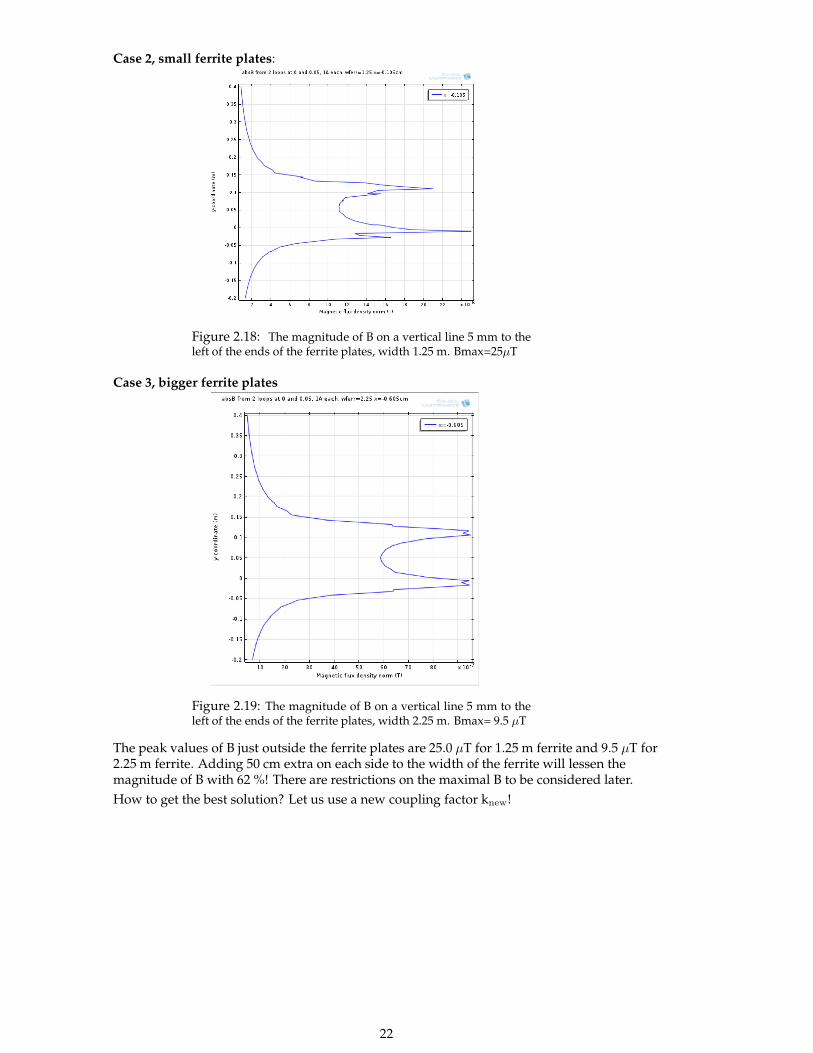
Case 2, small ferrite plates; only the left half of the field image shown:
Figure 2.15: The field lines between the two ferrite plates, drawn 0.1 moutside the two current loops. The centre of the plates at x=0.5 m.
20
Case 3, bigger ferrite plates; only the left half of the field image shown
Figure 2.16: The field lines between the two ferrite plates, drawn out0.6 m outside the two current loops. The centre of the plates at x=0.5 m
Result: From the field images we can see that short ferrite plates (drawn out 10 cm outsidethe windings) will give a high magnetic field close to the windings. This can give skin effectin the wires. We also get high magnetic field outside the geometry. More than 10 cm extraferrite will be necessary with all other parameters unchanged.
The magnitude of the B-field - leakage flux
It is also interesting to look for the maximal value of the B-field in space. It will occur justoutside the ends of the ferrite plates. Or more exact outside the upper face of the lower ferriteplate (lower face of the upper ferrite plate). The magnitude of the B-field is plotted on avertical line drawn 5 mm outside the ends of the screens, see figure 2.17. In the Figures 2.18and 2.19 the coordinate y is on the vertical and B on the horizontal axis.
5 mm
Figure 2.17: The ferrite planes and the windings. A vertical line isdrawn 5 mm outside the plates. The B-fields on this line are shown inthe next two figures.
21
Case 2, small ferrite plates:
Figure 2.18: The magnitude of B on a vertical line 5 mm to theleft of the ends of the ferrite plates, width 1.25 m. Bmax=25µT
Case 3, bigger ferrite plates
Figure 2.19: The magnitude of B on a vertical line 5 mm to theleft of the ends of the ferrite plates, width 2.25 m. Bmax= 9.5 µT
The peak values of B just outside the ferrite plates are 25.0 µT for 1.25 m ferrite and 9.5 µT for2.25 m ferrite. Adding 50 cm extra on each side to the width of the ferrite will lessen themagnitude of B with 62 %! There are restrictions on the maximal B to be considered later.
How to get the best solution? Let us use a new coupling factor knew!
22
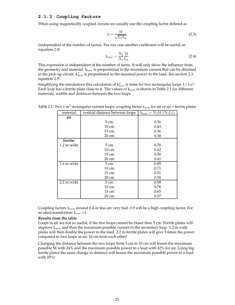
2.1.3 Coupling factors
When using magnetically coupled circuits we usually use the coupling factor defined as
k =M√L1L2
(2.3)
(independent of the number of turns). For our case another coefficient will be useful, seequation 2.4!
knew =N2
N1
M
L2
(2.4)
This expression is independent of the number of turns. It will only show the influence fromthe geometry and material. knew is proportional to the maximum current that can be obtainedin the pick-up circuit. k2
new is proportional to the maximal power to the load. See section 2.3,equation 2.5!
Simplifying the simulations this calculation of k2new is done for two rectangular loops 1×1m2.
Each loop has a ferrite plate close to it. The values of knew is shown in Table 2.1 for differentmaterials, widths and distances between the two loops.
Table 2.1: Two 1 m2 rectangular current loops: coupling factor knew for air or air + ferrite plates
material vertical distance between loops knew = N2M/(N1L2)air
5 cm 0.5610 cm 0.4315 cm 0.3620 cm 0.30
ferrite:1.2 m wide 5 cm 0.78
10 cm 0.6215 cm 0.5020 cm 0.41
1.6 m wide 5 cm 0.8510 cm 0.7115 cm 0.5120 cm 0.50
2.2 m wide 5 cm 0.8810 cm 0.7615 cm 0.6520 cm 0.57
Coupling factors knew around 0.4 or less are very bad. 0.9 will be a high coupling factor. Foran ideal transformer knew =1.
Results from the tableLoops in air are not so useful, if the two loops cannot be closer than 5 cm. Ferrite plates willimprove knew and thus the maximum possible current in the secondary loop. 1.2 m wideplates will then double the power to the load. 2.2 m ferrite plates will give 3 times the powercompared to two loops in air, 10 cm from each other!
Changing the distance between the two loops from 5 cm to 10 cm will lessen the maximumpossible M with 24% and the maximum possible power to a load with 42% for air. Using bigferrite plates the same change in distance will lessen the maximum possible power to a loadwith 25%!
23
2.1.4 Frequency dependence
The simulations above are done for a wire radius of 5 mm and at low frequencies. Choosing afrequency of 20 kHz we must look at the skin depth in the copper windings.δ20k = 4.67 · 10−4 m. We could use the radius of the wires a= 5·10−4 m. We also want to sendhigh currents so the wires must be in parallel in order to avoid too high current densities andalso lessen the the skin effect in the wires.
For a 3D design in the next section we will instead use flat wires, 5mm×0.2mm. Seecalculations later.
Using the power loss in the wires for definition of R and the vector potential for calculation ofL and M we can use the Comsol’s Multiphysics Magnetic Field(mf) or Magnetic and ElectricField (mef) applications, or the Maxwell program. (Errors in the built-in calculations of thecircuit parameters R, L and M still exist in both the programs, versions 4.3 and 15.0respectively. These parameters cannot be used in our case.)
It is difficult to use the model of many parallel wires in the windings in a 3D simulationbecause of the different length scales of windings and volumes for the magnetic fieldcalculations. We will make some simplifications, see next section!
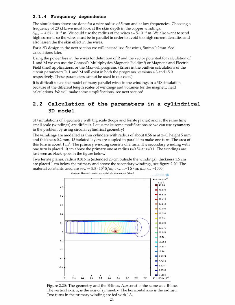
2.2 Calculation of the parameters in a cylindrical
3D model
3D simulations of a geometry with big scale (loops and ferrite planes) and at the same timesmall scale (windings) are difficult. Let us make some modifications so we can use symmetryin the problem by using circular cylindrical geometry!
The windings are modelled as thin cylinders with radius of about 0.56 m at z=0, height 5 mmand thickness 0.2 mm. 15 isolated layers are coupled in parallel to make one turn. The area ofthis turn is about 1 m2. The primary winding consists of 2 turn. The secondary winding withone turn is placed 10 cm above the primary one at radius r=0.54 at z=0.1. The windings arejust seen as black spots in the figure below.
Two ferrite planes, radius 0.816 m (extended 25 cm outside the windings), thickness 1.5 cmare placed 1 cm below the primary and above the secondary windings, see figure 2.20! Thematerial constants used are σCu = 5.8 · 107 S/m, σferrite=1 S/m; µrel,ferr =1000;
Figure 2.20: The geometry and the B-lines, Aφ=const is the same as a B-line.The vertical axis, z, is the axis of symmetry. The horizontal axis is the radius r.Two turns in the primary winding are fed with 1A.
24
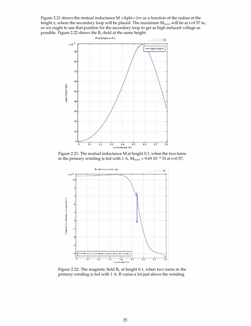
Figure 2.21 shows the mutual inductance M =Aphi×2πr as a function of the radius at theheight z, where the secondary loop will be placed. The maximum Mmax will be at r=0.57 m,so we ought to use that position for the secondary loop to get as high induced voltage aspossible. Figure 2.22 shows the Bz-field at the same height.
Figure 2.21: The mutual inductance M at height 0.1, when the two turnsin the primary winding is fed with 1 A. Mmax = 9.69 10−6 H at r=0.57.
Figure 2.22: The magnetic field Bz at height 0.1, when two turns in theprimary winding is fed with 1 A. B varies a lot just above the winding
25
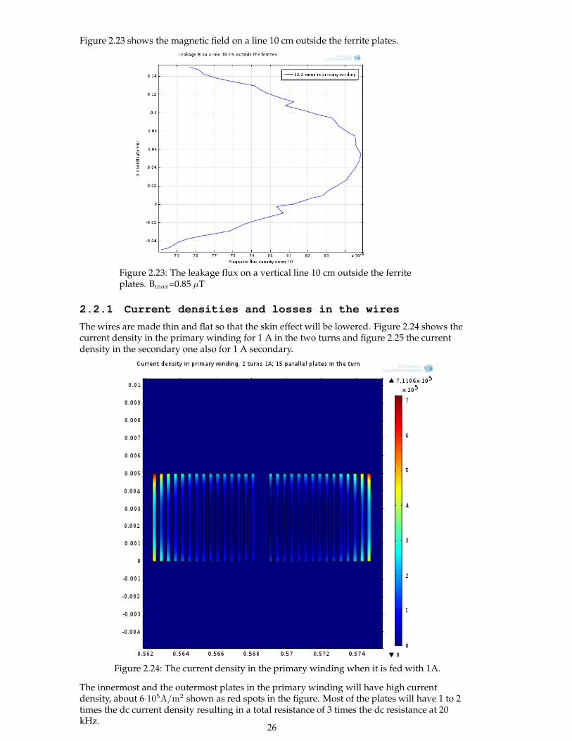
Figure 2.23 shows the magnetic field on a line 10 cm outside the ferrite plates.
Figure 2.23: The leakage flux on a vertical line 10 cm outside the ferriteplates. Bmax=0.85 µT
2.2.1 Current densities and losses in the wires
The wires are made thin and flat so that the skin effect will be lowered. Figure 2.24 shows thecurrent density in the primary winding for 1 A in the two turns and figure 2.25 the currentdensity in the secondary one also for 1 A secondary.
Figure 2.24: The current density in the primary winding when it is fed with 1A.
The innermost and the outermost plates in the primary winding will have high currentdensity, about 6·105A/m2 shown as red spots in the figure. Most of the plates will have 1 to 2times the dc current density resulting in a total resistance of 3 times the dc resistance at 20kHz.
26
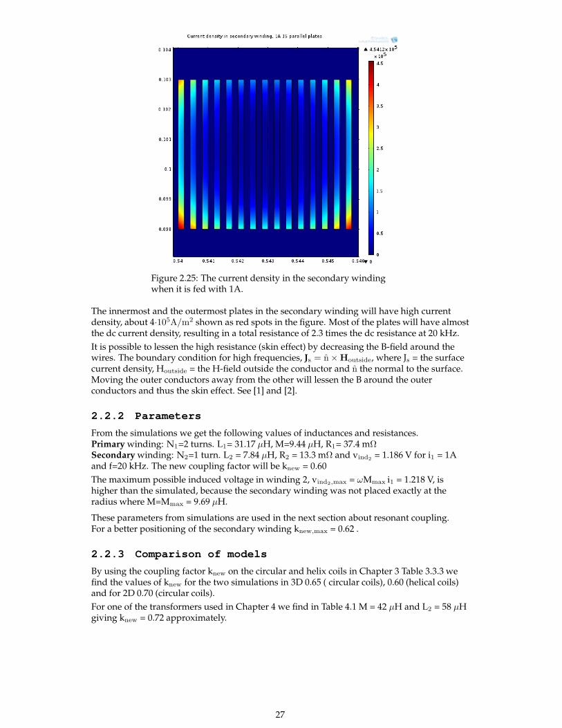
Figure 2.25: The current density in the secondary windingwhen it is fed with 1A.
The innermost and the outermost plates in the secondary winding will have high currentdensity, about 4·105A/m2 shown as red spots in the figure. Most of the plates will have almostthe dc current density, resulting in a total resistance of 2.3 times the dc resistance at 20 kHz.
It is possible to lessen the high resistance (skin effect) by decreasing the B-field around thewires. The boundary condition for high frequencies, Js = n×Houtside, where Js = the surfacecurrent density, Houtside = the H-field outside the conductor and n the normal to the surface.Moving the outer conductors away from the other will lessen the B around the outerconductors and thus the skin effect. See [1] and [2].
2.2.2 Parameters
From the simulations we get the following values of inductances and resistances.Primary winding: N1=2 turns. L1= 31.17 µH, M=9.44 µH, R1= 37.4 mΩSecondary winding: N2=1 turn. L2 = 7.84 µH, R2 = 13.3 mΩ and vind2
= 1.186 V for i1 = 1Aand f=20 kHz. The new coupling factor will be knew = 0.60
The maximum possible induced voltage in winding 2, vind2,max = ωMmax i1 = 1.218 V, ishigher than the simulated, because the secondary winding was not placed exactly at theradius where M=Mmax = 9.69 µH.
These parameters from simulations are used in the next section about resonant coupling.For a better positioning of the secondary winding knew,max = 0.62 .
2.2.3 Comparison of models
By using the coupling factor knew on the circular and helix coils in Chapter 3 Table 3.3.3 wefind the values of knew for the two simulations in 3D 0.65 ( circular coils), 0.60 (helical coils)and for 2D 0.70 (circular coils).
For one of the transformers used in Chapter 4 we find in Table 4.1 M = 42 µH and L2 = 58 µHgiving knew = 0.72 approximately.
27
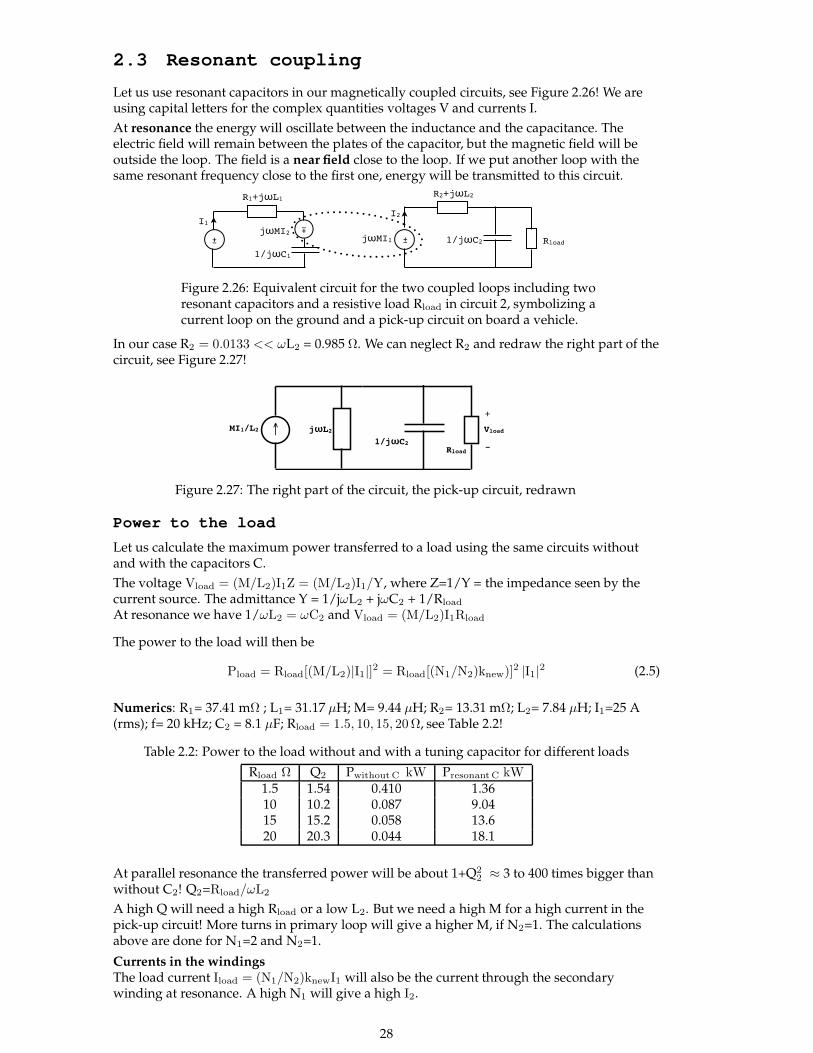
2.3 Resonant coupling
Let us use resonant capacitors in our magnetically coupled circuits, see Figure 2.26! We areusing capital letters for the complex quantities voltages V and currents I.
At resonance the energy will oscillate between the inductance and the capacitance. Theelectric field will remain between the plates of the capacitor, but the magnetic field will beoutside the loop. The field is a near field close to the loop. If we put another loop with thesame resonant frequency close to the first one, energy will be transmitted to this circuit.
I1
R1+jωL1
±
±
1/jωC1
jωMI2
I2
± 1/jωC2
R2+jωL2
RloadjωMI1
Figure 2.26: Equivalent circuit for the two coupled loops including tworesonant capacitors and a resistive load Rload in circuit 2, symbolizing acurrent loop on the ground and a pick-up circuit on board a vehicle.
In our case R2 = 0.0133 << ωL2 = 0.985 Ω. We can neglect R2 and redraw the right part of thecircuit, see Figure 2.27!
↑ jωL2
1/jωC2Rload
MI1/L2 Vload
+
-
Figure 2.27: The right part of the circuit, the pick-up circuit, redrawn
Power to the load
Let us calculate the maximum power transferred to a load using the same circuits withoutand with the capacitors C.
The voltage Vload = (M/L2)I1Z = (M/L2)I1/Y, where Z=1/Y = the impedance seen by thecurrent source. The admittance Y = 1/jωL2 + jωC2 + 1/Rload
At resonance we have 1/ωL2 = ωC2 and Vload = (M/L2)I1Rload
The power to the load will then be
Pload = Rload[(M/L2)|I1|]2 = Rload[(N1/N2)knew)]2 |I1|2 (2.5)
Numerics: R1= 37.41 mΩ ; L1= 31.17 µH; M= 9.44 µH; R2= 13.31 mΩ; L2= 7.84 µH; I1=25 A(rms); f= 20 kHz; C2 = 8.1 µF; Rload = 1.5, 10, 15, 20Ω, see Table 2.2!
Table 2.2: Power to the load without and with a tuning capacitor for different loads
Rload Ω Q2 PwithoutC kW PresonantC kW1.5 1.54 0.410 1.3610 10.2 0.087 9.0415 15.2 0.058 13.620 20.3 0.044 18.1
At parallel resonance the transferred power will be about 1+Q22 ≈ 3 to 400 times bigger than
without C2! Q2=Rload/ωL2
A high Q will need a high Rload or a low L2. But we need a high M for a high current in thepick-up circuit! More turns in primary loop will give a higher M, if N2=1. The calculationsabove are done for N1=2 and N2=1.
Currents in the windingsThe load current Iload = (N1/N2)knewI1 will also be the current through the secondarywinding at resonance. A high N1 will give a high I2.
28
Frequency dependence
At resonance the load power is independent of the frequency. However the frequency mustbe high enough to fulfill the requirements in the calculations above:
1. R2 ≪ ωL2 ;2. We must be able to find a capacitor for the resonant condition C2 = 1/(ω2L2)The higher the frequency, the more influence from the skin effect in the windings.
2.4 Conclusions of Chapter 2
Higher currents will need a better winding design. One way to lessen the skin effect in thewinding layers is to move the innermost and outermost layer away from the rest of thelayers. See for instance Figure 2.25. This will lessen the B-field around the wires and thus thehighest induced currents in these layers.
A horizontal displacement of 5 cm at a height of 10 cm will diminish the load power withapproximately 7 % .
Ferrite plates will improve knew and thus the maximum possible current in the secondaryloop. Big ferrite plates will give 3 times the power to a load compared to loops in air.
Changing the vertical distance between the two loops from 5 cm to 10 cm will lessen themaximum possible power to a load with 42% for air. Using big ferrite plates the same changein distance will lessen the maximum possible power to a load with 25%.
The coupling factor knew will give a way to compare the efficiency of the different geometriesand materials in the coil design.
Adding a resonant C to the secondary circuit the maximum transferred power will go up 3 to400 times.
29

30
Chapter 3
Modelling the wireless transfer
coil system into Ansys
A general wireless transfer coil system is modelled in the finite element program packageAnsys Maxwell, similar to that shown in Figure 3. The set-up consists of two coils, onetransmitting coil and one receiving coil. Adjacent to both coils there is a ferrite plate and analuminium plate. The model in Figure 3 is two-dimensional with axial symmetry, so that thecoils are represented as a set of circular coils, rather than a helix coil. A helix coil is also apossibility. Therefore, three-dimensional models are used to represent the problem set-up.
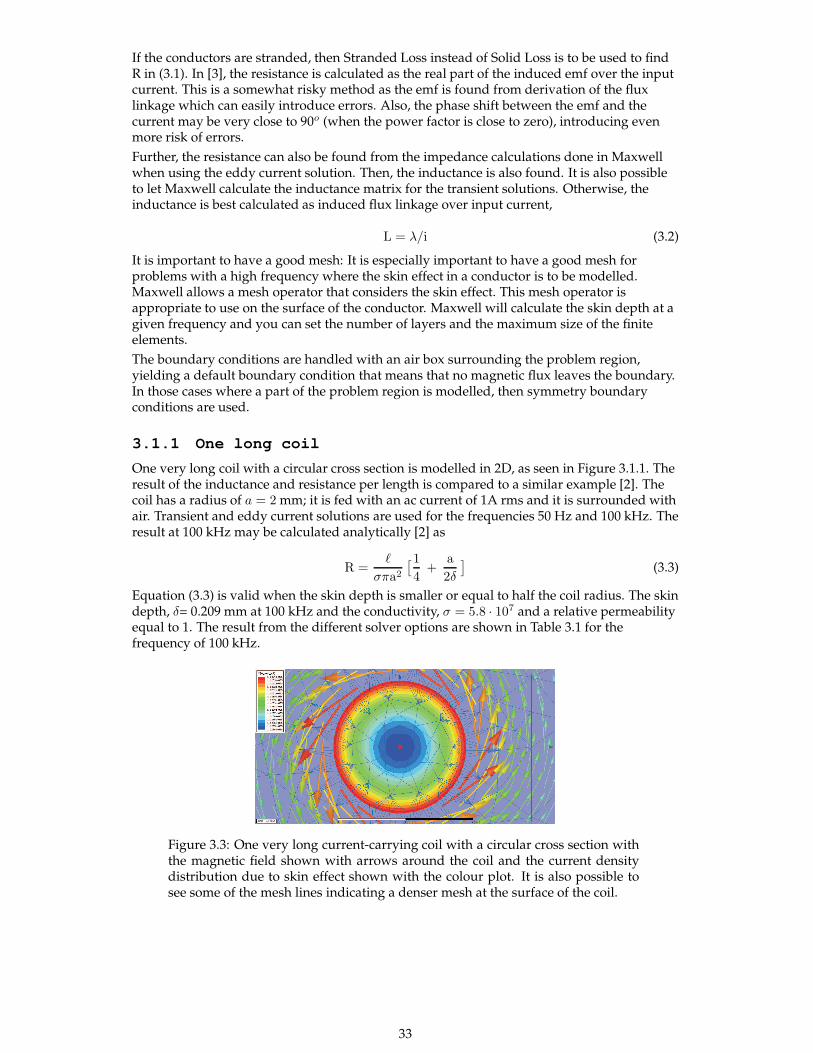
The 3D models are made with both helix coils and a set of circular coils in order to compare2D and 3D models. The models are verified against analytical calculations [2] and also tosome extent against a master thesis work [3] where a similar set-up is used. The purpose ofthe models is to calculate inductance values and resistances when skin effect and proximityeffects are considered. The results are also compared to measured results from a bachelorwork [4], where a part of the problem set-up (the emitting coils) is shown in Figure 3.2.
The solution types ”transient” and ”eddy current” were both used for 2D as well as 3Dproblems. The transient solution considers the time difference of the magnetic fields, inducedvoltages etc., allowing any kind of time-dependence, and consequently allowing severaltransmitting coils with different frequencies. On the other hand, the eddy current solverallows only magnetic fields varying sinusoidally in time (with one frequency); thus solvingthe steady-state problem. The displacement currents are in all cases neglected.
The model set-up, solution and post-processing are made with a script, written in VisualBasic within Microsoft Excel. Therefore, the input variables and dimensions can be variedfrom an Excel sheet.
31
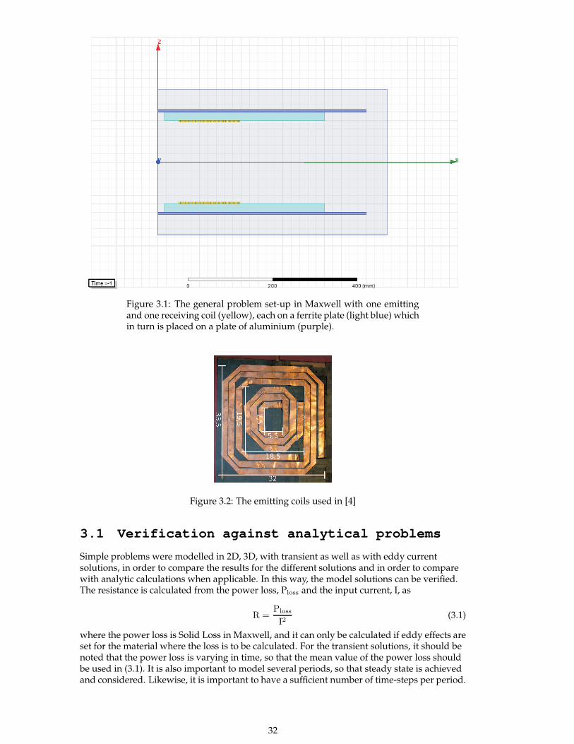
Figure 3.1: The general problem set-up in Maxwell with one emittingand one receiving coil (yellow), each on a ferrite plate (light blue) whichin turn is placed on a plate of aluminium (purple).
Figure 3.2: The emitting coils used in [4]
3.1 Verification against analytical problems
Simple problems were modelled in 2D, 3D, with transient as well as with eddy currentsolutions, in order to compare the results for the different solutions and in order to comparewith analytic calculations when applicable. In this way, the model solutions can be verified.The resistance is calculated from the power loss, Ploss and the input current, I, as
R =Ploss
I2(3.1)
where the power loss is Solid Loss in Maxwell, and it can only be calculated if eddy effects areset for the material where the loss is to be calculated. For the transient solutions, it should benoted that the power loss is varying in time, so that the mean value of the power loss shouldbe used in (3.1). It is also important to model several periods, so that steady state is achievedand considered. Likewise, it is important to have a sufficient number of time-steps per period.
32
If the conductors are stranded, then Stranded Loss instead of Solid Loss is to be used to findR in (3.1). In [3], the resistance is calculated as the real part of the induced emf over the inputcurrent. This is a somewhat risky method as the emf is found from derivation of the fluxlinkage which can easily introduce errors. Also, the phase shift between the emf and thecurrent may be very close to 90o (when the power factor is close to zero), introducing evenmore risk of errors.
Further, the resistance can also be found from the impedance calculations done in Maxwellwhen using the eddy current solution. Then, the inductance is also found. It is also possibleto let Maxwell calculate the inductance matrix for the transient solutions. Otherwise, theinductance is best calculated as induced flux linkage over input current,
L = λ/i (3.2)
It is important to have a good mesh: It is especially important to have a good mesh forproblems with a high frequency where the skin effect in a conductor is to be modelled.Maxwell allows a mesh operator that considers the skin effect. This mesh operator isappropriate to use on the surface of the conductor. Maxwell will calculate the skin depth at agiven frequency and you can set the number of layers and the maximum size of the finiteelements.
The boundary conditions are handled with an air box surrounding the problem region,yielding a default boundary condition that means that no magnetic flux leaves the boundary.In those cases where a part of the problem region is modelled, then symmetry boundaryconditions are used.
3.1.1 One long coil
One very long coil with a circular cross section is modelled in 2D, as seen in Figure 3.1.1. Theresult of the inductance and resistance per length is compared to a similar example [2]. Thecoil has a radius of a = 2 mm; it is fed with an ac current of 1A rms and it is surrounded withair. Transient and eddy current solutions are used for the frequencies 50 Hz and 100 kHz. Theresult at 100 kHz may be calculated analytically [2] as
R =ℓ
σπa2[1
4+
a
2δ
]
(3.3)
Equation (3.3) is valid when the skin depth is smaller or equal to half the coil radius. The skindepth, δ= 0.209 mm at 100 kHz and the conductivity, σ = 5.8 · 107 and a relative permeabilityequal to 1. The result from the different solver options are shown in Table 3.1 for thefrequency of 100 kHz.
Figure 3.3: One very long current-carrying coil with a circular cross section withthe magnetic field shown with arrows around the coil and the current densitydistribution due to skin effect shown with the colour plot. It is also possible tosee some of the mesh lines indicating a denser mesh at the surface of the coil.
33
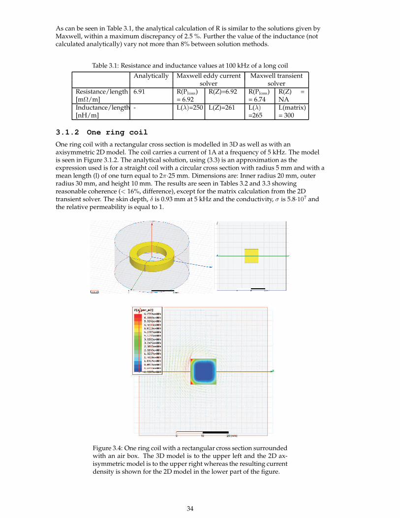
As can be seen in Table 3.1, the analytical calculation of R is similar to the solutions given byMaxwell, within a maximum discrepancy of 2.5 %. Further the value of the inductance (notcalculated analytically) vary not more than 8% between solution methods.
Table 3.1: Resistance and inductance values at 100 kHz of a long coil
Analytically Maxwell eddy current Maxwell transientsolver solver
Resistance/length[mΩ/m]
6.91 R(Ploss)= 6.92
R(Z)=6.92 R(Ploss)= 6.74
R(Z) =NA
Inductance/length[nH/m]
- L(λ)=250 L(Z)=261 L(λ)=265
L(matrix)= 300
3.1.2 One ring coil
One ring coil with a rectangular cross section is modelled in 3D as well as with anaxisymmetric 2D model. The coil carries a current of 1A at a frequency of 5 kHz. The modelis seen in Figure 3.1.2. The analytical solution, using (3.3) is an approximation as theexpression used is for a straight coil with a circular cross section with radius 5 mm and with amean length (l) of one turn equal to 2π·25 mm. Dimensions are: Inner radius 20 mm, outerradius 30 mm, and height 10 mm. The results are seen in Tables 3.2 and 3.3 showingreasonable coherence (< 16%, difference), except for the matrix calculation from the 2Dtransient solver. The skin depth, δ is 0.93 mm at 5 kHz and the conductivity, σ is 5.8·107 andthe relative permeability is equal to 1.
Figure 3.4: One ring coil with a rectangular cross section surroundedwith an air box. The 3D model is to the upper left and the 2D ax-isymmetric model is to the upper right whereas the resulting currentdensity is shown for the 2D model in the lower part of the figure.
34
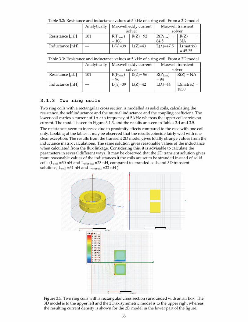
Table 3.2: Resistance and inductance values at 5 kHz of a ring coil. From a 3D model
Analytically Maxwell eddy current Maxwell transientsolver solver
Resistance [µΩ] 101 R(Ploss)= 106
R(Z)= 92 R(Ploss) =84.5
R(Z) =NA
Inductance [nH] — L(λ)=39 L(Z)=43 L(λ)=47.5 L(matrix)= 45.25
Table 3.3: Resistance and inductance values at 5 kHz of a ring coil. From a 2D model
Analytically Maxwell eddy current Maxwell transientsolver solver
Resistance [µΩ] 101 R(Ploss)= 96
R(Z)= 96 R(Ploss)= 94
R(Z) = NA
Inductance [nH] — L(λ)=39 L(Z)=42 L(λ)=44 L(matrix) =1850
3.1.3 Two ring coils
Two ring coils with a rectangular cross section is modelled as solid coils, calculating theresistance, the self inductance and the mutual inductance and the coupling coefficient. Thelower coil carries a current of 1A at a frequency of 5 kHz whereas the upper coil carries nocurrent. The model is seen in Figure 3.1.3, and the results are seen in Tables 3.4 and 3.5.
The resistances seem to increase due to proximity effects compared to the case with one coilonly. Looking at the tables it may be observed that the results coincide fairly well with oneclear exception: The results from the transient 2D model gives totally strange values from theinductance matrix calculations. The same solution gives reasonable values of the inductancewhen calculated from the flux linkage. Considering this, it is advisable to calculate theparameters in several different ways. It may be observed that the 2D transient solution givesmore reasonable values of the inductances if the coils are set to be stranded instead of solidcoils (Lself =50 nH and Lmutual =23 nH, compared to stranded coils and 3D transientsolutions; Lself =51 nH and Lmutual =22 nH ).
Figure 3.5: Two ring coils with a rectangular cross section surrounded with an air box. The3D model is to the upper left and the 2D axisymmetric model is to the upper right whereasthe resulting current density is shown for the 2D model in the lower part of the figure.
35
Table 3.4: Resistance and inductance values at 5 kHz of two ring coils. From a 3D model.
Maxwell eddy current Maxwell transientsolver 3D solver 3D
Resistance [µΩ] R(Ploss) = 107 R(Z)=123
R(Ploss) = 110 R(Z) =NA
Self inductance[nH]
L(λ)=37.4 L(Z)=39.5 L(λ)=43.4 L(matrix)= 40.0
Mutual induc-tance [nH]
L(λ)=20.8 L(Z)=21.8 L(λ)=22.7 L(matrix)= 23.0
Coupling coeffi-cient
0.549 0.542
Table 3.5: Resistance and inductance values at 5 kHz of two ring coils. From a 2D model.
Maxwell eddy current Maxwell transientsolver 2D solver 2D
Resistance [µΩ] R(Ploss) = 94.3 R(Z)=127
R(Ploss) = 124 R(Z) =NA
Self inductance[nH]
L(λ)=36.5 L(Z)=38.5 L(λ)=40.0 L(matrix)= 1850
Mutual induc-tance [nH]
L(λ)=21.6 L(Z)=22.1 L(λ)=22.1 L(matrix)= 842
Coupling coeffi-cient
0.574 0.55
3.2 Comparison to a master thesis work; two
ring coils with Ferrite and aluminium plates
One of the examples in [3] is used in order to compare results. The set-up, see Figure 3,consists of two copper coils with 25 turns (µr= 1 and σ = 5.8 · 107), one transmitting coil andone receiving coil. Symmetry may be used to constrain the problem region to half, having thesymmetry line along the x-axis. This is used for the resistance calculations. However, thenyou cannot calculate mutual inductance. Each coil cross section has a radius of 3.94 mm,according to [3]. However, the coils are represented with square cross section areas in theMaxwell models, as seen in Figure 3. Adjacent to both coils there is a ferrite plate (µr= 1000and σ = 1) and an aluminium plate (µr= 1 and σ = 3.54 · 107). The material properties areconstant and the problem is thus linear. The frequency is 40 kHz. The dimensions are givenin [3]. The skin depth of the copper coils, δCu = 0.33 mm at 40 kHz, and the skin depth of thealuminium and ferrite plates are, δAl = 0.42 mm and δFe= 79.5 mm, also at 40 kHz.
The coils in [3] are made of 200 strands of Litz-wire with a strand diameter of 0.2 mm, so thatthe Litz-wire does not eliminate the skin effect but reduce it. This poses some problems whencalculating the resistance, as the Litz-wire cannot practically be modelled as twisted, solidstrands. Therefore, the coils are either modelled as 25 stranded coils with 1 turn (assumingthat the Litz-wire cancels out the skin effect completely) or as 25 solid coils with 1 turn(assuming that there is full skin effect despite the Litz-wire). The true value of the resistanceshould then be between those found values.
There is also a question on what cross section area to choose for the coil. The coil radius is3.94 mm giving an area of π(3.94)2 mm2. However, with the Litz-wire considered, the areacan be as small as 200·π(0.2)2mm2 with a fill factor of 100%. Using a square cross section area,both cases are considered with two different values of the side of the square; 3.94 mm and 2.5mm. The coils are in both cases treated as solid coils, yielding a resistance of 1.2 Ω , and 0.6 Ωrespectively. The latter value is for the smaller cross section area. It would seem strange thatthe smaller cross section area gives a lower resistance. However, the smaller area gives alarger distance between coils and thus a smaller impact of the proximity effect.
36
If the same problems are solved with stranded coils, then the smaller cross section area givesa higher resistance (yielding a resistance of 0.022 Ω , and 0.054 Ω respectively where the lattervalue is for the smaller cross section area). It could therefore be concluded that if the coilshave no skin and proximity effects, then the resistance may be as low as 0.022 Ω , whereas ifthe coils are solid coils, and the proximity and skin effect is not minimized at all, then theresistance may be as high as 1.2 Ω . The resistance is in all cases calculated from the powerloss (either solid loss or stranded loss), as in eq. (3.1). However, in [3], the resistance iscalculated (to be 0.1 Ω ) as the real part of the induced voltage over the input current.
To calculate the inductance, the coils are modelled as stranded coils, thereby minimizing thecalculation time for the 3D transient solution and allowing a 2D transient solution. This isconsidered to be a reasonable approach as the inductance values are not much affected by theskin and proximity effects, as was seen in Section 3.1.2, although the self inductance was 20%higher for the stranded coils compared to the solid coil. The coils have a square cross sectionarea with length 3.94 mm. When modelling the problem as a steady state problem (with theeddy current solver), the 25 coils cannot be coupled to a winding, and thus is the inductancefor the whole winding complicated to calculate, using the 25 inductance-values. Therefore,the inductance is calculated from energy, W,
W =1
2Li2 (3.4)
yielding a value of 280 µH for the self inductance. This may be compared to a 3D transientsolution with solid coils yielding a self inductance of 277 µH, a mutual inductance of 56 µH,and a resistance of 0.12 Ω. The plot of the flux density from a 2D eddy current solution isshown together with a plot of the flux density from the transient 2D solution, showing verysimilar results, see Figure 3.2. Figure 3.7 shows the flux density distribution for the case witha 3D transient solution with solid coils. The impedance values are further calculated onlyfrom the transient solutions (both in 3D and 2D) with stranded coils, and the results are listedin Table 3.6 together with the results of [3]. In both Table 3.6 and Figures 3.2 and 3.7 and forvalues mentioned above, the results are similar regarding flux pattern and the inductances,whereas the resistance values are more astray due to the difficulty to model the Litz-wireproperly.
Table 3.6: Resistance and inductance values at 40 kHz of two stranded ring coils with 25 turns.
Maxwell transient Maxwell transient [3]solver 3D solver 2D
Resistance [Ω] R(Ploss) = 0.023 R(Ploss) = 0.02 0.1Self inductance[µH]
L(λ)=282 L(matrix)=282 L(λ)=278 L(matrix) =273
280
Mutual induc-tance [µH]
L(λ)=57 L(matrix)=57 L(λ)=57 L(matrix) =58
55
37
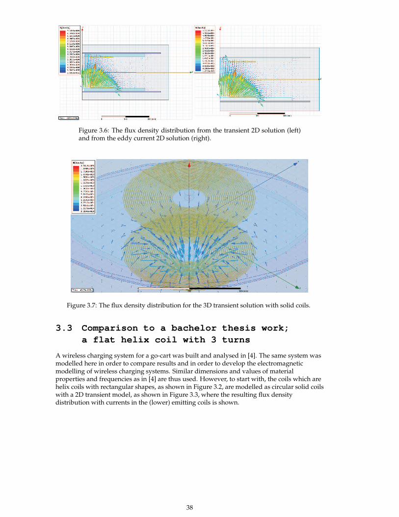
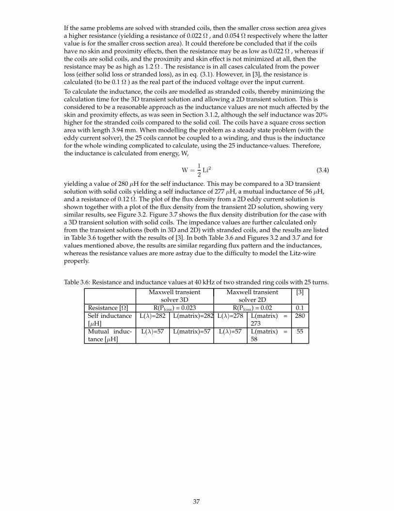
Figure 3.6: The flux density distribution from the transient 2D solution (left)and from the eddy current 2D solution (right).
Figure 3.7: The flux density distribution for the 3D transient solution with solid coils.
3.3 Comparison to a bachelor thesis work;
a flat helix coil with 3 turns
A wireless charging system for a go-cart was built and analysed in [4]. The same system wasmodelled here in order to compare results and in order to develop the electromagneticmodelling of wireless charging systems. Similar dimensions and values of materialproperties and frequencies as in [4] are thus used. However, to start with, the coils which arehelix coils with rectangular shapes, as shown in Figure 3.2, are modelled as circular solid coilswith a 2D transient model, as shown in Figure 3.3, where the resulting flux densitydistribution with currents in the (lower) emitting coils is shown.
38
Figure 3.8: The wireless charger with two lower emitting windings with three turnseach and a similar receiving coil set, with attached ferrite plates. The arrows showthe flux density distribution due to currents in the emitting windings, with a fre-quency of 100 kHz for the inner winding and 40 kHz for the outer winding.
3.3.1 2D axisymmetric transient model of a flat circular coil
with 3 turns
The wireless charging system consists of two emitting coils and two receiving coils, all fourcoils having 3 turns. The coils are attached to a ferrite plate with a relative permeability of1600. The coils are made of copper sheets with dimensions 0.2·20 mm. The dimensions of theemitting coils in [4] are seen in Figure 3.2. The dimension used for the circular coils arechosen so that the area of the emitting coils are similar. The receiving coils are modelled asmirrors of the emitting coils. See the used dimensions in Table 3.7.
Table 3.7: Dimensions of the wireless charging emitting coils used for the 2D model.
INNER COIL:Inner radius of inner emitting coil 36.2 mmDistance between turns 3.7 mmOuter radius of inner emitting coil 103.5 mm
OUTER COIL:Inner radius of outer emitting coil 107.2 mmDistance between turns 8.75 mmOuter radius of outer emitting coil 184.7 mm
FERRITE PLATE:Ferrite plate outer radius 350 mmFerrite plate height 20 mmDistance between upper and lower coils 40mm
The results of the inductance and resistance values are shown and compared to the measuredvalues in [4], in Table 3.8. The dc resistance of the coils are measured to be around 10-20 mΩ ,according to [4]. The calculated value from the model with circular coils at 50 Hz is 5.6 mΩfor the inner emitting coil and 11.8 mΩ, for the outer emitting coil. It is said in [4] that thecoils are not much affected by the skin and proximity effects due to the thinness of the copperconductors.
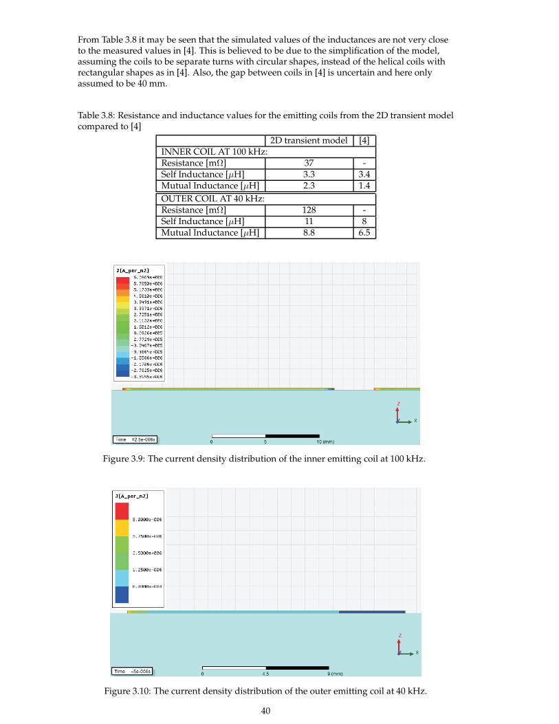
However, according to the simulations, the ac resistance at 100 kHz (37 mΩ) is about 7 timeslarger than the resistance at 50 Hz (5.6 mΩ). The effect may also be seen in Figure 3.9 andFigure 3.10 showing the current density distribution of the inner emitting coil at 100 kHz andouter emitting coil at 40 kHz, respectively.
39
From Table 3.8 it may be seen that the simulated values of the inductances are not very closeto the measured values in [4]. This is believed to be due to the simplification of the model,assuming the coils to be separate turns with circular shapes, instead of the helical coils withrectangular shapes as in [4]. Also, the gap between coils in [4] is uncertain and here onlyassumed to be 40 mm.
Table 3.8: Resistance and inductance values for the emitting coils from the 2D transient modelcompared to [4]
2D transient model [4]INNER COIL AT 100 kHz:Resistance [mΩ] 37 -Self Inductance [µH] 3.3 3.4Mutual Inductance [µH] 2.3 1.4
OUTER COIL AT 40 kHz:Resistance [mΩ] 128 -Self Inductance [µH] 11 8Mutual Inductance [µH] 8.8 6.5
Figure 3.9: The current density distribution of the inner emitting coil at 100 kHz.
Figure 3.10: The current density distribution of the outer emitting coil at 40 kHz.
40
3.3.2 A 3D transient model of a flat circular coil with 3
separate turns
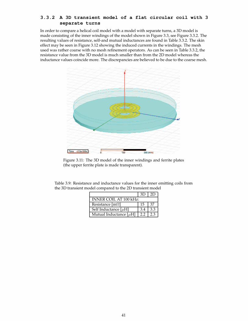
In order to compare a helical coil model with a model with separate turns, a 3D model ismade consisting of the inner windings of the model shown in Figure 3.3, see Figure 3.3.2. Theresulting values of resistance, self-and mutual inductances are found in Table 3.3.2. The skineffect may be seen in Figure 3.12 showing the induced currents in the windings. The meshused was rather coarse with no mesh refinement operators. As can be seen in Table 3.3.2, theresistance value from the 3D model is much smaller than from the 2D model whereas theinductance values coincide more. The discrepancies are believed to be due to the coarse mesh.
Figure 3.11: The 3D model of the inner windings and ferrite plates(the upper ferrite plate is made transparent).
Table 3.9: Resistance and inductance values for the inner emitting coils fromthe 3D transient model compared to the 2D transient model
3D 2DINNER COIL AT 100 kHz:Resistance [mΩ] 15 37Self Inductance [µH] 3.4 3.3Mutual Inductance [µH] 2.2 2.3
41
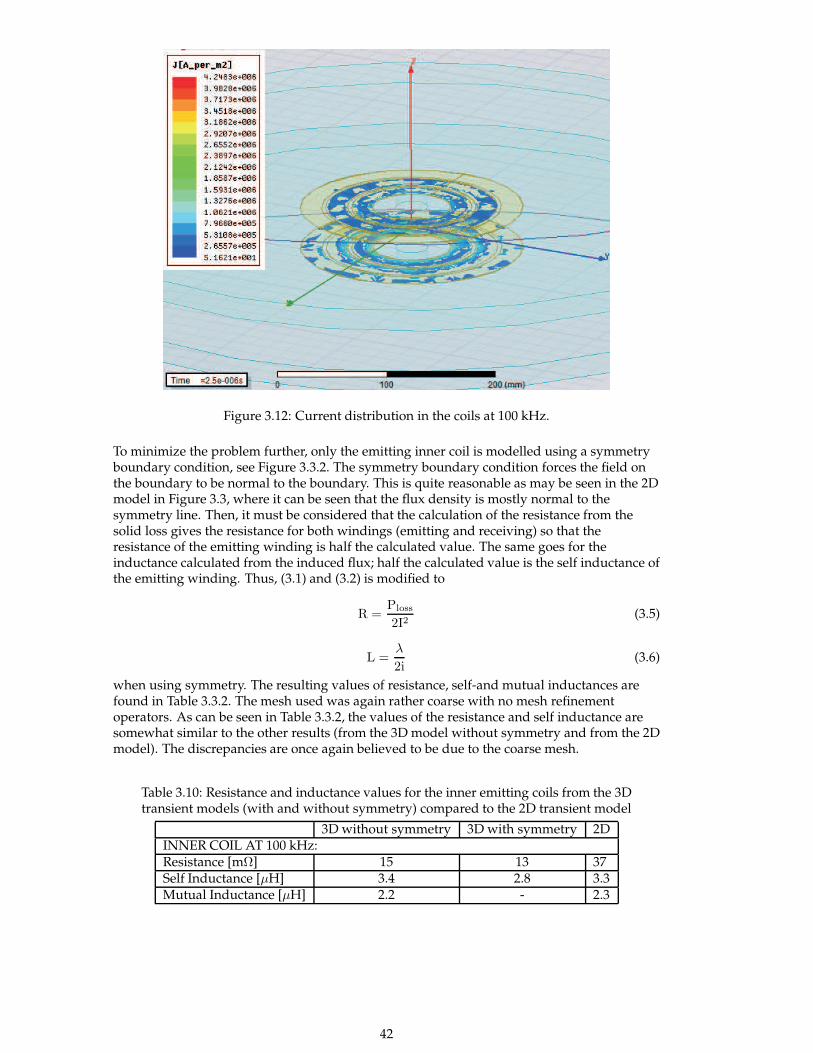
Figure 3.12: Current distribution in the coils at 100 kHz.
To minimize the problem further, only the emitting inner coil is modelled using a symmetryboundary condition, see Figure 3.3.2. The symmetry boundary condition forces the field onthe boundary to be normal to the boundary. This is quite reasonable as may be seen in the 2Dmodel in Figure 3.3, where it can be seen that the flux density is mostly normal to thesymmetry line. Then, it must be considered that the calculation of the resistance from thesolid loss gives the resistance for both windings (emitting and receiving) so that theresistance of the emitting winding is half the calculated value. The same goes for theinductance calculated from the induced flux; half the calculated value is the self inductance ofthe emitting winding. Thus, (3.1) and (3.2) is modified to
R =Ploss
2I2(3.5)
L =λ
2i(3.6)
when using symmetry. The resulting values of resistance, self-and mutual inductances arefound in Table 3.3.2. The mesh used was again rather coarse with no mesh refinementoperators. As can be seen in Table 3.3.2, the values of the resistance and self inductance aresomewhat similar to the other results (from the 3D model without symmetry and from the 2Dmodel). The discrepancies are once again believed to be due to the coarse mesh.
Table 3.10: Resistance and inductance values for the inner emitting coils from the 3Dtransient models (with and without symmetry) compared to the 2D transient model
3D without symmetry 3D with symmetry 2DINNER COIL AT 100 kHz:Resistance [mΩ] 15 13 37Self Inductance [µH] 3.4 2.8 3.3Mutual Inductance [µH] 2.2 - 2.3
42
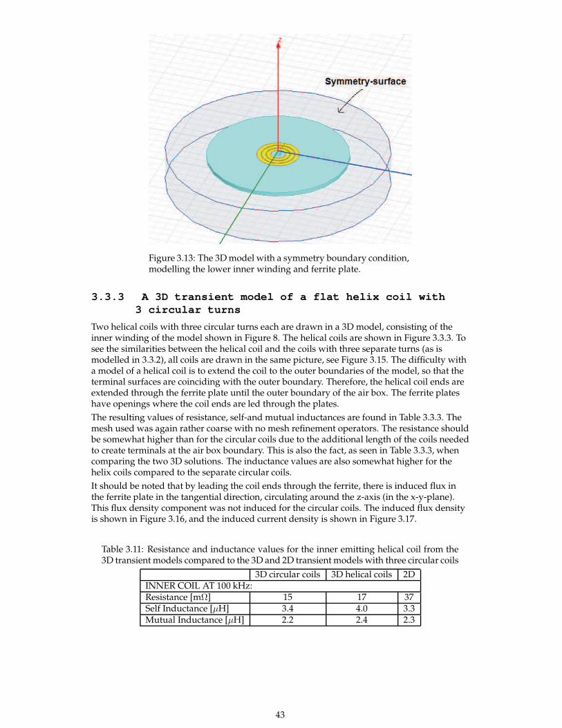
Figure 3.13: The 3D model with a symmetry boundary condition,modelling the lower inner winding and ferrite plate.
3.3.3 A 3D transient model of a flat helix coil with
3 circular turns
Two helical coils with three circular turns each are drawn in a 3D model, consisting of theinner winding of the model shown in Figure 8. The helical coils are shown in Figure 3.3.3. Tosee the similarities between the helical coil and the coils with three separate turns (as ismodelled in 3.3.2), all coils are drawn in the same picture, see Figure 3.15. The difficulty witha model of a helical coil is to extend the coil to the outer boundaries of the model, so that theterminal surfaces are coinciding with the outer boundary. Therefore, the helical coil ends areextended through the ferrite plate until the outer boundary of the air box. The ferrite plateshave openings where the coil ends are led through the plates.
The resulting values of resistance, self-and mutual inductances are found in Table 3.3.3. Themesh used was again rather coarse with no mesh refinement operators. The resistance shouldbe somewhat higher than for the circular coils due to the additional length of the coils neededto create terminals at the air box boundary. This is also the fact, as seen in Table 3.3.3, whencomparing the two 3D solutions. The inductance values are also somewhat higher for thehelix coils compared to the separate circular coils.
It should be noted that by leading the coil ends through the ferrite, there is induced flux inthe ferrite plate in the tangential direction, circulating around the z-axis (in the x-y-plane).This flux density component was not induced for the circular coils. The induced flux densityis shown in Figure 3.16, and the induced current density is shown in Figure 3.17.
Table 3.11: Resistance and inductance values for the inner emitting helical coil from the3D transient models compared to the 3D and 2D transient models with three circular coils
3D circular coils 3D helical coils 2DINNER COIL AT 100 kHz:Resistance [mΩ] 15 17 37Self Inductance [µH] 3.4 4.0 3.3Mutual Inductance [µH] 2.2 2.4 2.3
43

Figure 3.14: Two helix coils attached to ferrite plates, and surroundedwith an air box. The ferrite plates (light blue) have openings where thecoil ends are extended to the outer boundary of the air box.
Figure 3.15: The helix coil compared to the three separate coils used in section 3.3.2
Figure 3.16: Flux density distribution in the helix coils at 100 kHz44
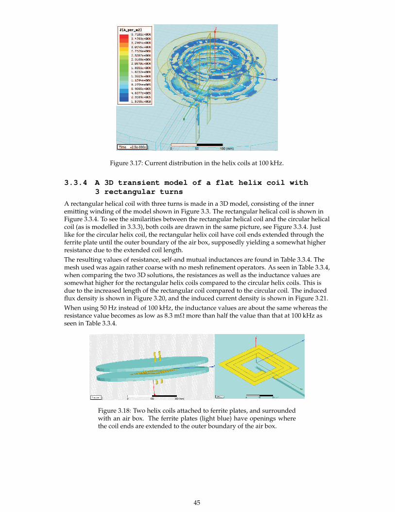
Figure 3.17: Current distribution in the helix coils at 100 kHz.
3.3.4 A 3D transient model of a flat helix coil with
3 rectangular turns
A rectangular helical coil with three turns is made in a 3D model, consisting of the inneremitting winding of the model shown in Figure 3.3. The rectangular helical coil is shown inFigure 3.3.4. To see the similarities between the rectangular helical coil and the circular helicalcoil (as is modelled in 3.3.3), both coils are drawn in the same picture, see Figure 3.3.4. Justlike for the circular helix coil, the rectangular helix coil have coil ends extended through theferrite plate until the outer boundary of the air box, supposedly yielding a somewhat higherresistance due to the extended coil length.
The resulting values of resistance, self-and mutual inductances are found in Table 3.3.4. Themesh used was again rather coarse with no mesh refinement operators. As seen in Table 3.3.4,when comparing the two 3D solutions, the resistances as well as the inductance values aresomewhat higher for the rectangular helix coils compared to the circular helix coils. This isdue to the increased length of the rectangular coil compared to the circular coil. The inducedflux density is shown in Figure 3.20, and the induced current density is shown in Figure 3.21.
When using 50 Hz instead of 100 kHz, the inductance values are about the same whereas theresistance value becomes as low as 8.3 mΩ more than half the value than that at 100 kHz asseen in Table 3.3.4.
Figure 3.18: Two helix coils attached to ferrite plates, and surroundedwith an air box. The ferrite plates (light blue) have openings wherethe coil ends are extended to the outer boundary of the air box.
45
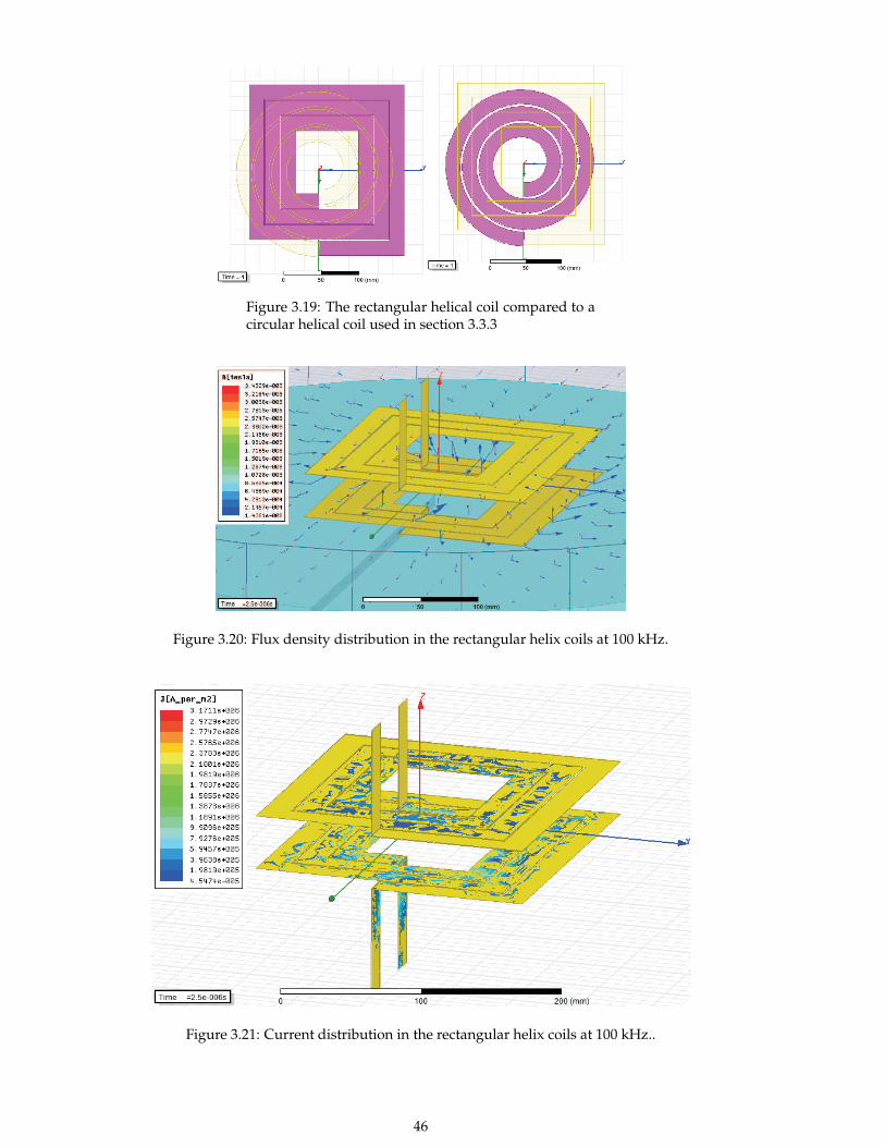
Figure 3.19: The rectangular helical coil compared to acircular helical coil used in section 3.3.3
Figure 3.20: Flux density distribution in the rectangular helix coils at 100 kHz.
Figure 3.21: Current distribution in the rectangular helix coils at 100 kHz..
46
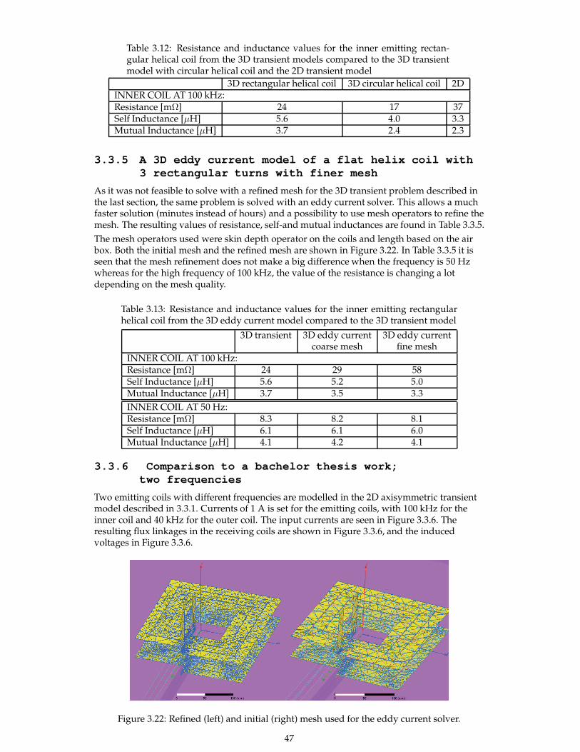
Table 3.12: Resistance and inductance values for the inner emitting rectan-gular helical coil from the 3D transient models compared to the 3D transientmodel with circular helical coil and the 2D transient model
3D rectangular helical coil 3D circular helical coil 2DINNER COIL AT 100 kHz:Resistance [mΩ] 24 17 37Self Inductance [µH] 5.6 4.0 3.3Mutual Inductance [µH] 3.7 2.4 2.3
3.3.5 A 3D eddy current model of a flat helix coil with
3 rectangular turns with finer mesh
As it was not feasible to solve with a refined mesh for the 3D transient problem described inthe last section, the same problem is solved with an eddy current solver. This allows a muchfaster solution (minutes instead of hours) and a possibility to use mesh operators to refine themesh. The resulting values of resistance, self-and mutual inductances are found in Table 3.3.5.
The mesh operators used were skin depth operator on the coils and length based on the airbox. Both the initial mesh and the refined mesh are shown in Figure 3.22. In Table 3.3.5 it isseen that the mesh refinement does not make a big difference when the frequency is 50 Hzwhereas for the high frequency of 100 kHz, the value of the resistance is changing a lotdepending on the mesh quality.
Table 3.13: Resistance and inductance values for the inner emitting rectangularhelical coil from the 3D eddy current model compared to the 3D transient model
3D transient 3D eddy current 3D eddy currentcoarse mesh fine mesh
INNER COIL AT 100 kHz:Resistance [mΩ] 24 29 58Self Inductance [µH] 5.6 5.2 5.0Mutual Inductance [µH] 3.7 3.5 3.3
INNER COIL AT 50 Hz:Resistance [mΩ] 8.3 8.2 8.1Self Inductance [µH] 6.1 6.1 6.0Mutual Inductance [µH] 4.1 4.2 4.1
3.3.6 Comparison to a bachelor thesis work;
two frequencies
Two emitting coils with different frequencies are modelled in the 2D axisymmetric transientmodel described in 3.3.1. Currents of 1 A is set for the emitting coils, with 100 kHz for theinner coil and 40 kHz for the outer coil. The input currents are seen in Figure 3.3.6. Theresulting flux linkages in the receiving coils are shown in Figure 3.3.6, and the inducedvoltages in Figure 3.3.6.
Figure 3.22: Refined (left) and initial (right) mesh used for the eddy current solver.
47
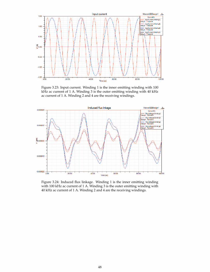
Figure 3.23: Input current. Winding 1 is the inner emitting winding with 100kHz ac current of 1 A. Winding 3 is the outer emitting winding with 40 kHzac current of 1 A. Winding 2 and 4 are the receiving windings.
Figure 3.24: Induced flux linkage. Winding 1 is the inner emitting windingwith 100 kHz ac current of 1 A. Winding 3 is the outer emitting winding with40 kHz ac current of 1 A. Winding 2 and 4 are the receiving windings.
48
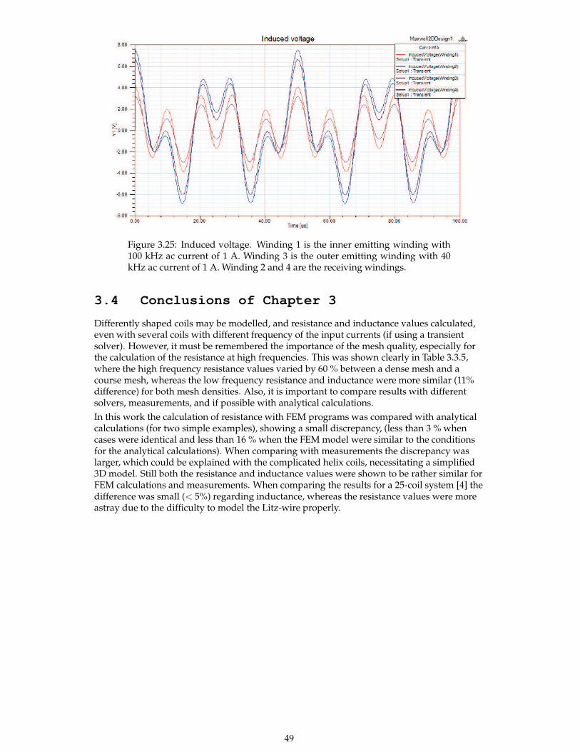
Figure 3.25: Induced voltage. Winding 1 is the inner emitting winding with100 kHz ac current of 1 A. Winding 3 is the outer emitting winding with 40kHz ac current of 1 A. Winding 2 and 4 are the receiving windings.
3.4 Conclusions of Chapter 3
Differently shaped coils may be modelled, and resistance and inductance values calculated,even with several coils with different frequency of the input currents (if using a transientsolver). However, it must be remembered the importance of the mesh quality, especially forthe calculation of the resistance at high frequencies. This was shown clearly in Table 3.3.5,where the high frequency resistance values varied by 60 % between a dense mesh and acourse mesh, whereas the low frequency resistance and inductance were more similar (11%difference) for both mesh densities. Also, it is important to compare results with differentsolvers, measurements, and if possible with analytical calculations.
In this work the calculation of resistance with FEM programs was compared with analyticalcalculations (for two simple examples), showing a small discrepancy, (less than 3 % whencases were identical and less than 16 % when the FEM model were similar to the conditionsfor the analytical calculations). When comparing with measurements the discrepancy waslarger, which could be explained with the complicated helix coils, necessitating a simplified3D model. Still both the resistance and inductance values were shown to be rather similar forFEM calculations and measurements. When comparing the results for a 25-coil system [4] thedifference was small (< 5%) regarding inductance, whereas the resistance values were moreastray due to the difficulty to model the Litz-wire properly.
49

50
Chapter 4
Wireless charger unit
4.1 Overview of charger
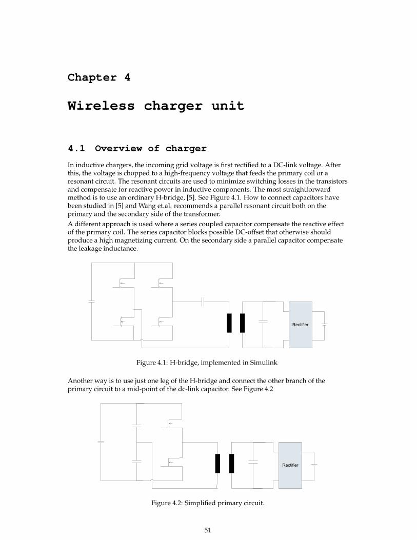
In inductive chargers, the incoming grid voltage is first rectified to a DC-link voltage. Afterthis, the voltage is chopped to a high-frequency voltage that feeds the primary coil or aresonant circuit. The resonant circuits are used to minimize switching losses in the transistorsand compensate for reactive power in inductive components. The most straightforwardmethod is to use an ordinary H-bridge, [5]. See Figure 4.1. How to connect capacitors havebeen studied in [5] and Wang et.al. recommends a parallel resonant circuit both on theprimary and the secondary side of the transformer.
A different approach is used where a series coupled capacitor compensate the reactive effectof the primary coil. The series capacitor blocks possible DC-offset that otherwise shouldproduce a high magnetizing current. On the secondary side a parallel capacitor compensatethe leakage inductance.
Rectifier
Figure 4.1: H-bridge, implemented in Simulink
Another way is to use just one leg of the H-bridge and connect the other branch of theprimary circuit to a mid-point of the dc-link capacitor. See Figure 4.2
Rectifier
Figure 4.2: Simplified primary circuit.
51
In this section we will study a case with a 100 kW power level, which is a suitable level forcharging a plug-in bus.
Incoming voltage is 400 V +/- 10 % which means that the DC-link voltage has a nominalvalue of Udc = 540− 650V , depending on if we have a diode rectifier or a transistor converter.We assume a battery voltage that is changing between 250 V and 400 V depending on state ofcharge.
4.2 Transformer
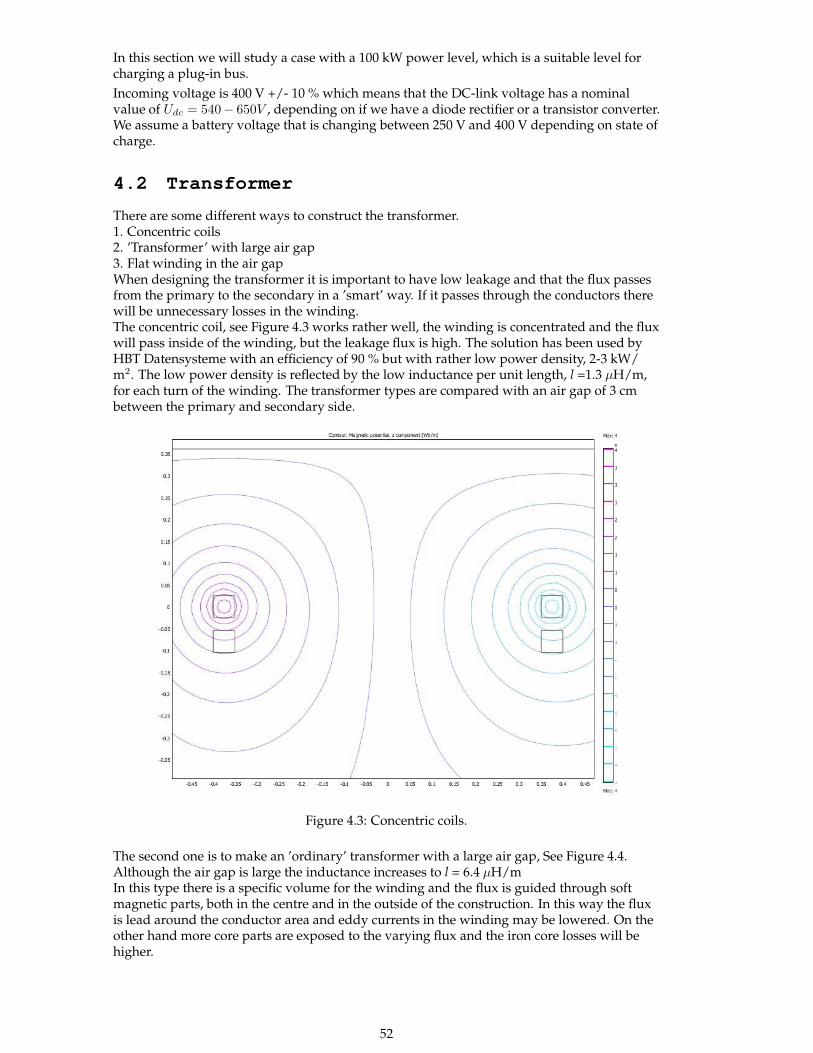
There are some different ways to construct the transformer.1. Concentric coils2. ’Transformer’ with large air gap3. Flat winding in the air gapWhen designing the transformer it is important to have low leakage and that the flux passesfrom the primary to the secondary in a ’smart’ way. If it passes through the conductors therewill be unnecessary losses in the winding.The concentric coil, see Figure 4.3 works rather well, the winding is concentrated and the fluxwill pass inside of the winding, but the leakage flux is high. The solution has been used byHBT Datensysteme with an efficiency of 90 % but with rather low power density, 2-3 kW/m2. The low power density is reflected by the low inductance per unit length, l =1.3 µH/m,for each turn of the winding. The transformer types are compared with an air gap of 3 cmbetween the primary and secondary side.
Figure 4.3: Concentric coils.
The second one is to make an ’ordinary’ transformer with a large air gap, See Figure 4.4.Although the air gap is large the inductance increases to l = 6.4 µH/mIn this type there is a specific volume for the winding and the flux is guided through softmagnetic parts, both in the centre and in the outside of the construction. In this way the fluxis lead around the conductor area and eddy currents in the winding may be lowered. On theother hand more core parts are exposed to the varying flux and the iron core losses will behigher.
52
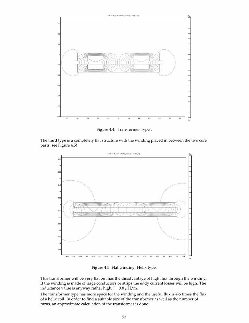
Figure 4.4: ’Transformer Type’.
The third type is a completely flat structure with the winding placed in between the two coreparts, see Figure 4.5!
Figure 4.5: Flat winding. Helix type.
This transformer will be very flat but has the disadvantage of high flux through the winding.If the winding is made of large conductors or strips the eddy current losses will be high. Theinductance value is anyway rather high, l = 3.8 µH/m.
The transformer type has more space for the winding and the useful flux is 4-5 times the fluxof a helix coil. In order to find a suitable size of the transformer as well as the number ofturns, an approximate calculation of the transformer is done.
53
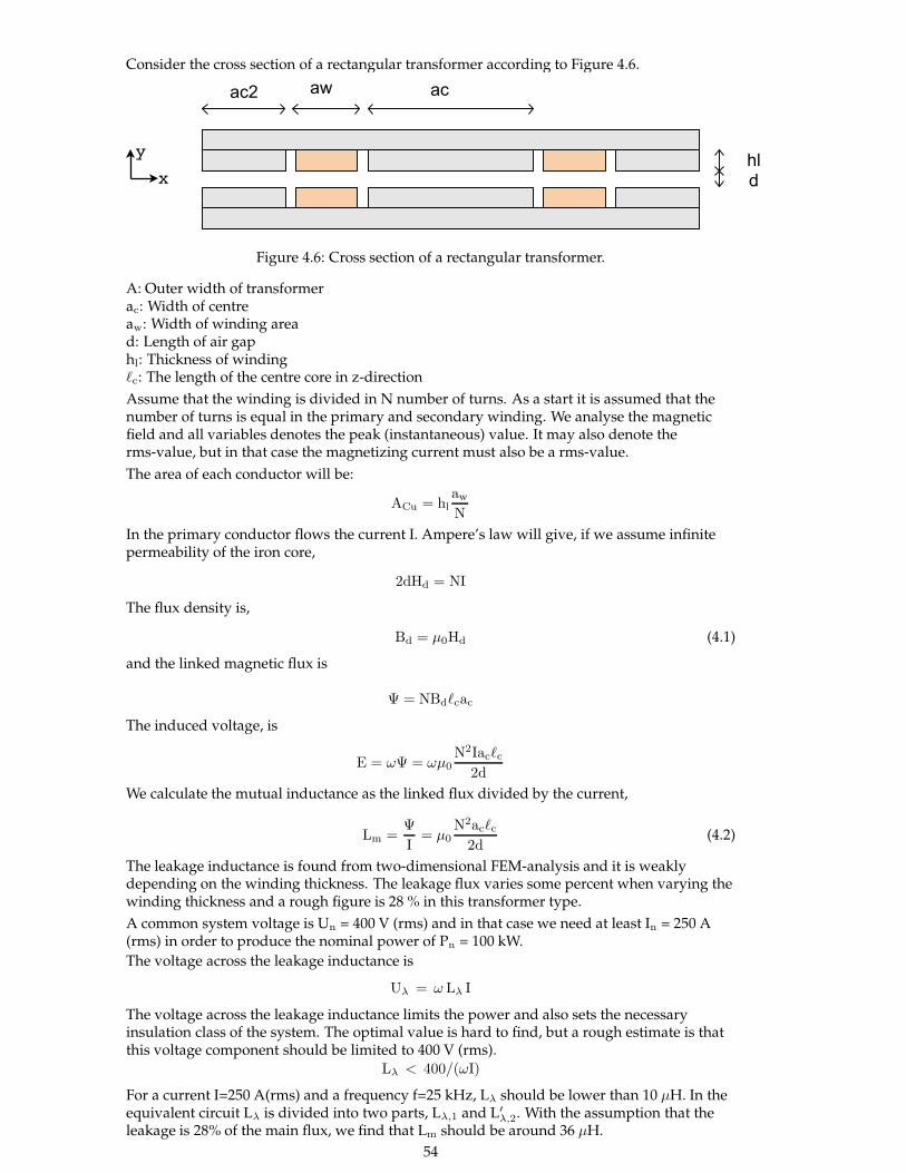
Consider the cross section of a rectangular transformer according to Figure 4.6.
acawac2
hl
dx
y
Figure 4.6: Cross section of a rectangular transformer.
A: Outer width of transformerac: Width of centreaw: Width of winding aread: Length of air gaphl: Thickness of windingℓc: The length of the centre core in z-direction
Assume that the winding is divided in N number of turns. As a start it is assumed that thenumber of turns is equal in the primary and secondary winding. We analyse the magneticfield and all variables denotes the peak (instantaneous) value. It may also denote therms-value, but in that case the magnetizing current must also be a rms-value.
The area of each conductor will be:
ACu = hlawN
In the primary conductor flows the current I. Ampere’s law will give, if we assume infinitepermeability of the iron core,
2dHd = NI
The flux density is,
Bd = µ0Hd (4.1)
and the linked magnetic flux is
Ψ = NBdℓcac
The induced voltage, is
E = ωΨ = ωµ0
N2Iacℓc2d
We calculate the mutual inductance as the linked flux divided by the current,
Lm =Ψ
I= µ0
N2acℓc2d
(4.2)
The leakage inductance is found from two-dimensional FEM-analysis and it is weaklydepending on the winding thickness. The leakage flux varies some percent when varying thewinding thickness and a rough figure is 28 % in this transformer type.
A common system voltage is Un = 400 V (rms) and in that case we need at least In = 250 A(rms) in order to produce the nominal power of Pn = 100 kW.
The voltage across the leakage inductance is
Uλ = ω Lλ I
The voltage across the leakage inductance limits the power and also sets the necessaryinsulation class of the system. The optimal value is hard to find, but a rough estimate is thatthis voltage component should be limited to 400 V (rms).
Lλ < 400/(ωI)
For a current I=250 A(rms) and a frequency f=25 kHz, Lλ should be lower than 10 µH. In theequivalent circuit Lλ is divided into two parts, Lλ,1 and L′
λ,2. With the assumption that theleakage is 28% of the main flux, we find that Lm should be around 36 µH.
54
Calculations on the transformer in Figure 4.6. Results are presented in Table 4.1
1. The inductances: The geometric quantities for the transformer are given in the table.Assuming N=7 (equal number of turns in the primary and secondary windings), equation(4.2) will give Lm = 42 µH. For 28% leakage flux the two equal leakage inductances Lλ,1 = L′
λ,2
will approximately be 16 µH each.
2. The B-field: Assuming a magnetizing current I=100 A (top value) equation (4.1) will givethe flux density Bd100 = 0.015 T. (Two dimensional FEM-calculations 0.0165 T.)This is rather low for core materials as ferrites. This means that the sizing of the transformeris more governed by leakage flux and the ability to work even if the bus is misaligned to thefixed core part. Leakage flux has to be low, otherwise the voltage over the leakage inductancewill limit the transformer power. Another thing that needs to considered is that amisalignment lowers the coupling and also alters the resonant circuit in a way that lowers thepossible power transfer, see section 2.1.1!
The misalignment and the distance the bus can be misaligned is related to the overalldimensions of the transformer and the air gap. With the data below in the table, it is assumedthat the misalignment can be almost 1 dm in the bus moving directions and some centimetresin the orthogonal direction.
3. Power losses in the core: The flux density in the back iron core is:
Bc =Ψ/N
2hc lc
And the power losses related to this flux density in the iron core is:
Pc = 400B2cmc
[7], where mc is the weight of the core material.
4. Power losses in the windings: The losses in the winding is partly ohmic losses, Pcu = RI2 ,where I is the rms-value. The resistance R= ρcuLwind/Acu and in this case the total length ofthe primary winding Lwind = 11.2 m.
As mentioned, the flux density in some transformer parts are low so there should not be anyproblem with losses in the core material. The power losses in the back iron can of course behigh if the core is thin. The leakage flux that is developed when the transformer is loaded willhowever be a problem. See Figure 4.2.
The leakage flux will induce eddy currents in the windings if the conductor dimensions arehigher than the skin depth. Compare with chapter 3, where equivalent resistance has beencalculated!
The power losses due to eddy currents in the windings may be approximated as:
Phf = Vcu
(ωdcuBx)2
32ρcu,
where VCu is the copper volume, [8].
The flux density is around Bx=0.02 T and the frequency is high so the overall diameter of theconductor dcu should be less than 0.3 mm in order to have a reasonable power loss due to theeddy current. The value calculated in Table 4.1 is calculated under the assumption of adiameter of 0.3 mm and Bx=0.02 T. As shown in Figure 4.2 a lot of flux passes the winding inthe case of a loaded transformer. This is partly due to the large air gap. How this shall besolved is just partly handled in this report and the calculated value is an approximative value.
55
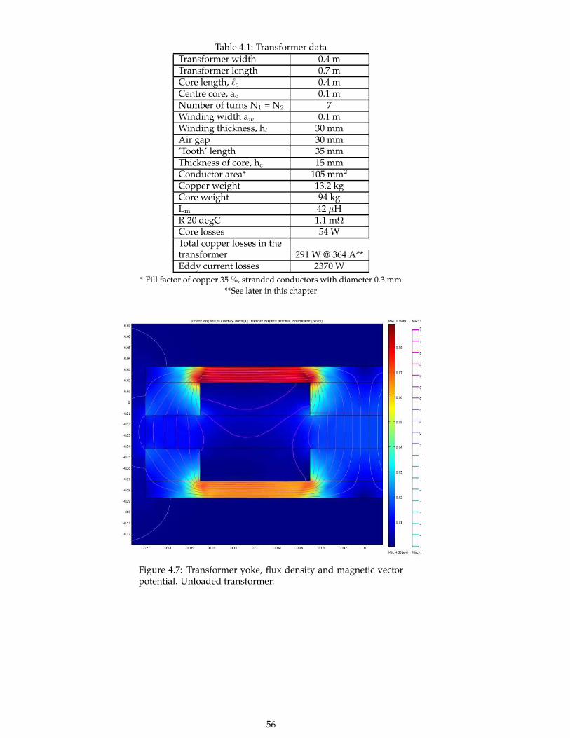
Table 4.1: Transformer data
Transformer width 0.4 mTransformer length 0.7 mCore length, ℓc 0.4 mCentre core, ac 0.1 mNumber of turns N1 = N2 7Winding width aw 0.1 mWinding thickness, hl 30 mmAir gap 30 mm’Tooth’ length 35 mmThickness of core, hc 15 mmConductor area* 105 mm2
Copper weight 13.2 kgCore weight 94 kgLm 42 µHR 20 degC 1.1 mΩCore losses 54 WTotal copper losses in thetransformer 291 W @ 364 A**Eddy current losses 2370 W
* Fill factor of copper 35 %, stranded conductors with diameter 0.3 mm
**See later in this chapter
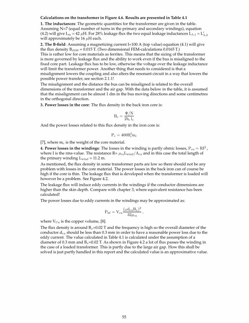
Figure 4.7: Transformer yoke, flux density and magnetic vectorpotential. Unloaded transformer.
56
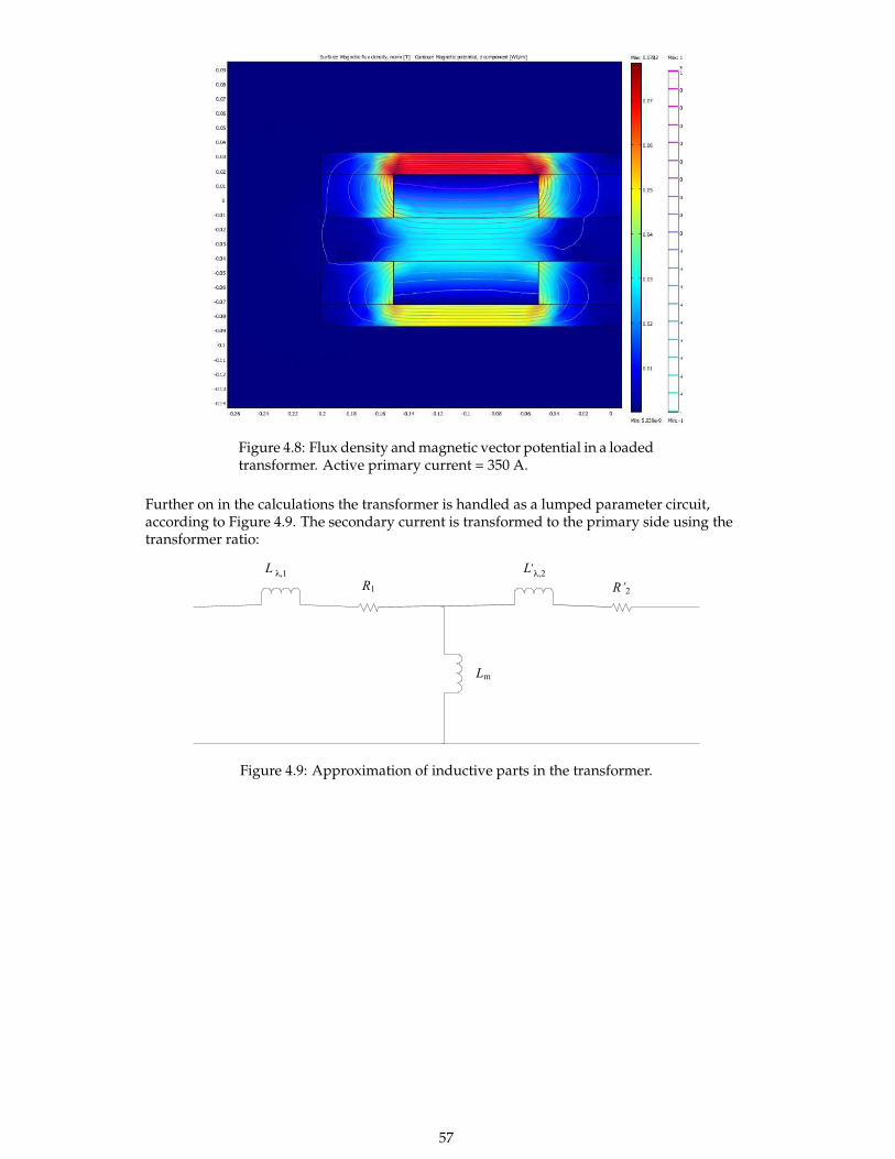
Figure 4.8: Flux density and magnetic vector potential in a loadedtransformer. Active primary current = 350 A.
Further on in the calculations the transformer is handled as a lumped parameter circuit,according to Figure 4.9. The secondary current is transformed to the primary side using thetransformer ratio:
L1
R1
L’2
R’2
Lm
λ,1’λ,2
Figure 4.9: Approximation of inductive parts in the transformer.
57
4.3 Power Electronics
For the time being IGBT:s are probably the best choice for controlling the current to thetransformer.The power losses of the power IGBT:s are approximated from data sheets as function ofcurrent, voltage and switching frequency. The switching losses are represented by a secondorder polynomial and the coefficients are found through the Matlab function ’polyfit’,producing the coefficients a0, a1 and a2. The circuit is simulated and at every switching eventit is decided whether or not it is an On-event, is there a diode involved or if it is an Off-event.One IGBT-module from Semikron and one from Infineon are compared.
Eon = a0 + a1i + a2i2
The conduction losses are,
p(t)cond = Ut0i(t) + rti(t)2
and the value is integrated over the simulation interval. The integrated value is divided bythe simulation time and the latter is chosen as an integer number of the fundamental periodtime.
Table 4.2: Data of different IGBT-components
Parameter SKM200GB123D/Semikron FF200R12KS/InfineonUt0 1.5 V 1.7 Vrt 10.7 mΩ 7.2 mΩUd0 1.0 V 1.3 Vrd 5.7 mΩ 2.9 mΩEon/On-switch energy /mJ a0=3.26, a1=0.058, a2 = 0.5e-3 a0=5.57, a1 = 0.016, a2=0.3e-3Eoff /Off-switch energy/mJ a0=3.39, a1=0.078, a2=0.1e-3 a0=0.17, a1=0.044, a2= 0.1e-3Err/reverse recovery/mJ a0=-0.14, a1= 0.078, a2= 0.2e-3 a0=2.01, a1= 0.063, a2= 0.1e-3
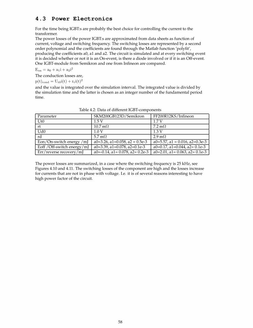
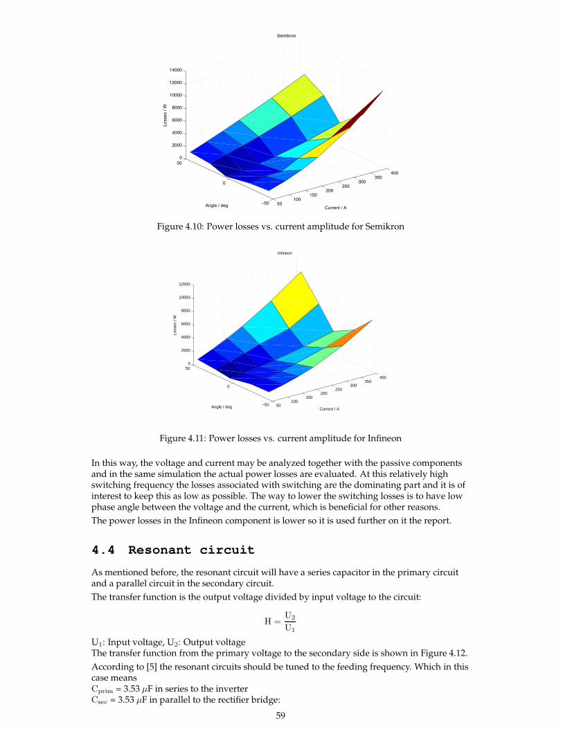
The power losses are summarized, in a case where the switching frequency is 25 kHz, seeFigures 4.10 and 4.11. The switching losses of the component are high and the losses increasefor currents that are not in phase with voltage. I.e. it is of several reasons interesting to havehigh power factor of the circuit.
58
!"#""
#!"$""
$!"%""
%!"&""
!!"
"
!"
"
$"""
&"""
'"""
("""
#""""
#$"""
#&"""
)*++,-./0/1
2,345+6-
1-78,/0/9,7
:6;;,;/0/<
Figure 4.10: Power losses vs. current amplitude for Semikron
50100
150200
250300
350400
−50
0
500
2000
4000
6000
8000
10000
12000
Current / A
Infineon
Angle / deg
Loss
es /
W
Figure 4.11: Power losses vs. current amplitude for Infineon
In this way, the voltage and current may be analyzed together with the passive componentsand in the same simulation the actual power losses are evaluated. At this relatively highswitching frequency the losses associated with switching are the dominating part and it is ofinterest to keep this as low as possible. The way to lower the switching losses is to have lowphase angle between the voltage and the current, which is beneficial for other reasons.
The power losses in the Infineon component is lower so it is used further on it the report.
4.4 Resonant circuit
As mentioned before, the resonant circuit will have a series capacitor in the primary circuitand a parallel circuit in the secondary circuit.
The transfer function is the output voltage divided by input voltage to the circuit:
H =U2
U1
U1: Input voltage, U2: Output voltageThe transfer function from the primary voltage to the secondary side is shown in Figure 4.12.
According to [5] the resonant circuits should be tuned to the feeding frequency. Which in thiscase meansCprim = 3.53 µF in series to the inverterCsec = 3.53 µF in parallel to the rectifier bridge:
59

Bode Diagram
Frequency (rad/sec)
105
−180
−90
0
90
180
Pha
se (
deg)
−40
−30
−20
−10
0
10
20
30
Mag
nitu
de (
dB)
Figure 4.12: Bode analysis of transfer function H. Load resistance 2.2, 5, 10, 20 Ω
4.5 Control of transformer current
One way to control the converter is to measure the current and wait for the zero-crossing andthen switch the transistors. In this way the frequency will vary but low switching-losses areachieved over the range of load variations. Figure 4.13 shows current and voltage when thiscontrol strategy is applied in a fictive circuit, it works well but it has to be fine-tuned withappropriate circuit parameters.
Figure 4.13: Converter output at current control.
60
Another way to avoid switching losses is to add a capacitor across every IGBT and alwayscontrol it in inductive region. I.e. the current is always lagging the voltage with a small angle.In this case the frequency has to be chosen in such a way that we always have a current that islagging the voltage.
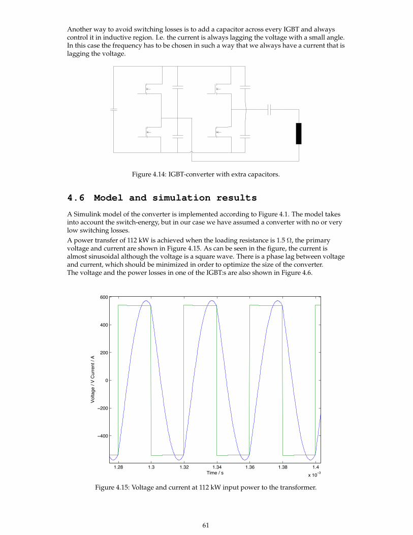
Figure 4.14: IGBT-converter with extra capacitors.
4.6 Model and simulation results
A Simulink model of the converter is implemented according to Figure 4.1. The model takesinto account the switch-energy, but in our case we have assumed a converter with no or verylow switching losses.
A power transfer of 112 kW is achieved when the loading resistance is 1.5 Ω, the primaryvoltage and current are shown in Figure 4.15. As can be seen in the figure, the current isalmost sinusoidal although the voltage is a square wave. There is a phase lag between voltageand current, which should be minimized in order to optimize the size of the converter.The voltage and the power losses in one of the IGBT:s are also shown in Figure 4.6.
!"#$ !"% !"%# !"%& !"%' !"%$ !"&
()!*!%
!&**
!#**
*
#**
&**
'**
+,-.)/)0
123456.)/)1)7899.:4)/);
Figure 4.15: Voltage and current at 112 kW input power to the transformer.
61
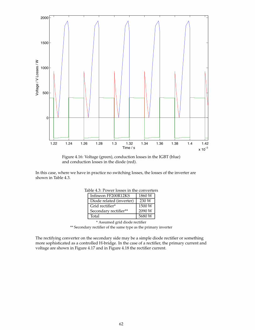
!"## !"#$ !"#% !"#& !"' !"'# !"'$ !"'% !"'& !"$ !"$#
()!*!'
*
+**
!***
!+**
#***
,-./)0)1
234567/)0)2)8311/1)0)9
Figure 4.16: Voltage (green), conduction losses in the IGBT (blue)and conduction losses in the diode (red).
In this case, where we have in practice no switching losses, the losses of the inverter areshown in Table 4.3.
Table 4.3: Power losses in the converters
Infineon FF200R12KS 1860 WDiode related (inverter) 230 WGrid rectifier* 1500 WSecondary rectifier** 2090 WTotal 5680 W
* Assumed grid diode rectifier
** Secondary rectifier of the same type as the primary inverter
The rectifying converter on the secondary side may be a simple diode rectifier or somethingmore sophisticated as a controlled H-bridge. In the case of a rectifier, the primary current andvoltage are shown in Figure 4.17 and in Figure 4.18 the rectifier current.
62

!"# !"## !"#$ !"#% !"#& !"' !"'# !"'$ !"'%
()!*!'
!%**
!$**
!#**
*
#**
$**
%**
+,-.)/)0
123456.)/)1)7899.:4)/);
Figure 4.17: Primary voltage and current
0 1 2 3 4 5
x 10−4
0
100
200
300
400
500
Time / s
Rec
tifie
r cu
rren
t / A
Figure 4.18: Rectifier current.
The circuit filters the rectifier current in an efficient way.
63
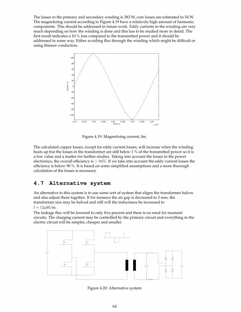
The losses in the primary and secondary winding is 383 W, core losses are estimated to 54 W.The magnetizing current according to Figure 4.19 have a relatively high amount of harmoniccomponents. This should be addressed in future work. Eddy currents in the winding are verymuch depending on how the winding is done and this has to be studied more in detail. Thefirst result indicates a 10 % loss compared to the transmitted power and it should beaddressed in some way. Either avoiding flux through the winding which might be difficult orusing thinner conductors.
2.21 2.215 2.22 2.225 2.23 2.235 2.24 2.245 2.25
x 10−3
−100
−80
−60
−40
−20
0
20
40
60
80
100
Time / s
Cur
rent
/ A
Figure 4.19: Magnetizing current, Im.
The calculated copper losses, except for eddy current losses, will increase when the windingheats up but the losses in the transformer are still below 1 % of the transmitted power so it isa low value and a matter for further studies. Taking into account the losses in the powerelectronics, the overall efficiency is > 94%. If we take into account the eddy current losses theefficiency is below 90 %. It is based on some simplified assumptions and a more thoroughcalculation of the losses is necessary.
4.7 Alternative system
An alternative to this system is to use some sort of system that aligns the transformer halvesand also adjust them together. If for instance the air gap is decreased to 3 mm, thetransformer size may be halved and still will the inductance be increased to
l = 12µH/m.
The leakage flux will be lowered to only five percent and there is no need for resonantcircuits. The charging current may be controlled by the primary circuit and everything in theelectric circuit will be simpler, cheaper and smaller.
Figure 4.20: Alternative system
64
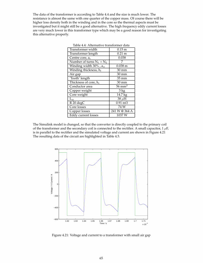
The data of the transformer is according to Table 4.4 and the size is much lower. Theresistance is almost the same with one quarter of the copper mass. Of course there will behigher loss density both in the winding and in the core so the thermal aspects must beinvestigated but it might still be a good alternative. The high frequency eddy current lossesare very much lower in this transformer type which may be a good reason for investigatingthis alternative properly.
Table 4.4: Alternative transformer data
Transformer width 0.15 mTransformer length 0.21 mCentre core, ac 0.038Number of turns N1 = N2 7Winding width 30% , aw 0.038 mWinding thickness, hl 30 mmAir gap 30 mm’Tooth’ length 35 mmThickness of core, hc 30 mmConductor area 56 mm2
Copper weight 3 kgCore weight 14.7 kgLm 38 µHR 20 degC 0.91 mΩCore losses 74 WCopper losses 241 W @ 364 AEddy current losses 1037 W
The Simulink model is changed, so that the converter is directly coupled to the primary coilof the transformer and the secondary coil is connected to the rectifier. A small capacitor, 1 µF,is in parallel to the rectifier and the simulated voltage and current are shown in Figure 4.21The resulting data of the circuit are highlighted in Table 4.5.
1.62 1.63 1.64 1.65 1.66 1.67 1.68 1.69 1.7 1.71
x 10−3
−600
−400
−200
0
200
400
600
Time / s
Vol
tage
/ V
Cur
rent
/ A
Figure 4.21: Voltage and current to a transformer with small air gap
65
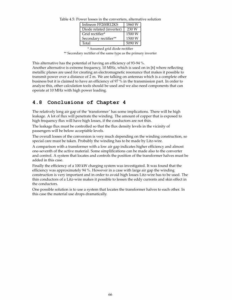
Table 4.5: Power losses in the converters, alternative solution
Infineon FF200R12KS 1860 WDiode related (inverter) 230 WGrid rectifier* 1500 WSecondary rectifier** 1500 WTotal 5090 W
* Assumed grid diode rectifier
** Secondary rectifier of the same type as the primary inverter
This alternative has the potential of having an efficiency of 93-94 %.Another alternative is extreme frequency, 10 MHz, which is used on in [6] where reflectingmetallic planes are used for creating an electromagnetic resonance that makes it possible totransmit power over a distance of 2 m. We are talking on antennas which is a complete otherbusiness but it is claimed to have an efficiency of 97 % in the transmission part. In order toanalyze this, other calculation tools should be used and we also need components that canoperate at 10 MHz with high power loading.
4.8 Conclusions of Chapter 4
The relatively long air gap of the ’transformer’ has some implications. There will be highleakage. A lot of flux will penetrate the winding. The amount of copper that is exposed tohigh frequency flux will have high losses, if the conductors are not thin.
The leakage flux must be controlled so that the flux density levels in the vicinity ofpassengers will be below acceptable levels.
The overall losses of the conversion is very much depending on the winding construction, sospecial care must be taken. Probably the winding has to be made by Litz-wire.
A comparison with a transformer with a low air gap indicates higher efficiency and almostone-seventh of the active material. Some simplifications can be made also to the converterand control. A system that locates and controls the position of the transformer halves must beadded in this case.
Finally the efficiency of a 100 kW charging system was investigated. It was found that theefficiency was approximately 94 %. However in a case with large air gap the windingconstruction is very important and in order to avoid high losses Litz-wire has to be used. Thethin conductors of a Litz-wire makes it possible to lessen the eddy currents and skin effect inthe conductors.
One possible solution is to use a system that locates the transformer halves to each other. Inthis case the material use drops dramatically.
66
Chapter 5
Conclusions
In this work the theory of wireless charging was developed. FEM analyses on both 2D and3D models were performed using Maxwell and Comsol Multiphysics. Moreover, analyticalmethods were also developed and compared with the FEM results and some key results werecompared with measurements.
The larger the air gap between a receiving and a sending coil, the less sensitivity todisplacements, but also less mutual inductance. Less sensitivity can also be achieved if thecoils of the receiving coil are placed next to each other. This is shown more effective thanplacing the coils as one inner ring coil inside an outer ring coil. It is also shown better thanplacing the receiving coils above each other.
Further, it is shown efficient to use ferrite plates adjacent to the coils. The plates need to belarge in order to avoid high magnetic fields outside the charging system, as the maximumvalue of the magnetic field will occur just outside the ends of the ferrite plates.
It is also shown that if the coils (sending and/or receiving) have several conductors , then it isbest to move the outer conductors away as this will reduce the skin effect, and thereforereduce the coil resistance.
Adding a resonant C to the secondary circuit will raise the transmitted power up to 400 timeswhen using a resonant set-up.
Differently shaped coils may be modelled, and resistance and inductance values calculated.The mesh quality is shown important, especially for the calculation of the resistance at highfrequencies. It is also important to compare the results with different solvers, measurementsand if possible with analytical calculations.
Inductance and resistance of one and two ring coils were determined analytically with twosolvers in Maxwell with very accurate results. When comparing with measurements thediscrepancy was larger, which could be explained with the complicated helix coils,necessitating a simplified 3D model. Still both the resistance and inductance values wereshown to be rather similar for FEM calculations and measurements. When comparing theresults for a 25-coil system, the difference was small (<5%) regarding inductance, whereasthe resistance values were more astray due to the difficulty to model the Litz-wire properly.
The relatively long air gap of the ’transformer’ has some implications. There will be highleakage. A lot of flux will penetrate the winding. The amount of copper that is exposed tohigh frequency flux will have high losses, if the conductors are not thin. The leakage fluxmust be controlled so that the flux density levels in the vicinity of passengers will be belowacceptable levels.
Finally the efficiency of a 100 kW charging system was investigated. It was found that theefficiency was approximately 94 %. However in a case with a large air gap, the windingconstruction is very important and in order to avoid high losses Litz-wire has to be used. Thethin conductors of a Litz-wire makes it possible to lessen the eddy currents and skin effect inthe conductors. One possible solution is to use a system that locates the transformer halves toeach other. In this case the material use drops dramatically.
67

68

Bibliography
[1] Eva Palmberg, Lecture notes in Electromagnetic Design Course, Chalmers 2012
[2] Eva Palmberg 2012, ”Electromagnetics Revised” Course Compendium at the division ofElectric Power Engineering, the department of Energy and Environment at ChalmersUniversity of Technology, Goteborg, Sweden 2012.
[3] Mikael Cederlof (2012) ”Inductive Charging of Electrical Vehicles”, Master Thesis at KTHElectrical Engineering, Stockholm, Sweden 2012.
[4] Bjorkman Jimmy, Ekman Christian, Gustavsson Erik, Hagman Niklas, Hansson Gustav,and Majdandzic Davor (2012) ”Tradlos multifrekvensladdare for el-gocart”, BachelorThesis at the division of Electric Power Engineering, the department of Energy andEnvironment at Chalmers University of Technology, Goteborg, Sweden 2012.
[5] Wang, Stielau, Covic ”Design Considerations for a Contactless Electric Vehicle BatteryCharger”, IEEE Transactions on Industrial Electronics, vol.52 No.5 Oct-05
[6] Xiaofang Yu, Sunil Sandhu, Sven Beiker, Richard Sassoon and Shannui Fan ”Wirelessenergy transfer with the presence of metallic planes”, Appl.Phys. Lett. 99, 214102 (2011);doi: 10.1063/1.3663576
[7] Data sheet from EPCOS u 141 78 30.pdf
[8] Charles R. Sullivan, Member IEEE, Computationally Efficient Winding Loss Calculationwith Multiple Windings, Arbitrary Waveforms and Two-Dimensional orThree-Dimensional Field Geometry, IEEE Transactions on Power Electronics, vol. 16,No 1, January 2001
69