window coating absorbance spectra
DESCRIPTION
Window Coating Absorbance Spectra. Lisa Pawlowicz 17 August 2010. Overview. Materials and Methods Absorbance of Substrates Absorbance due to In 2 O 3 (ITO) Absorbance due to MgO Topics for Further Investigation. Window Coatings. 1.22” diameter. 50 Å MgO. 45 Å In 2 O 3 (ITO). - PowerPoint PPT PresentationTRANSCRIPT

Window Coating Absorbance Spectra
Lisa Pawlowicz17 August 2010
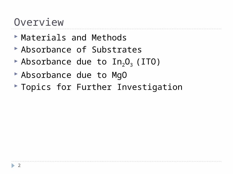
Overview Materials and Methods Absorbance of Substrates Absorbance due to In2O3 (ITO) Absorbance due to MgO Topics for Further Investigation
2

Window Coatings
.098” Fused Silica
45 Å In2O3 (ITO)
50 Å MgO1.22” diameter
• Windows cut by Oswald Siegmund at SSL• Coatings applied by Joe Libera at Argonne
• coatings applied to one side but (likely) diffused onto both
45 Å In2O3 (ITO)50 Å MgO
.098” Borofloat(Sn doped on one side)
OR
3

Absorbance Spectrum Scans
A - absorbanceI0 – intensity of incident lightI – intensity of transmitted lightα – attenuation coefficientx – optical path length
(thickness)T - transmission
Measuring absolute absorbance: no scaling factor
Instrument ParametersMeasurement Type: Wavelength ScanStarting Wavelength: 800.00 nmEnding Wavelength: 200.00 nmScan Speed: 300 nm/minSampling Interval: 1.00 nmHigh ResolutionPath Length: 2.0 mm (window thickness 2.5 mm)
Absorbance scans done with a Hitachi U-3010 spectrophotometer:
http://home.uevora.pt/~filmflc/GQS_Equipment_eng.htm4

200 300 400 500 600 700 800nm
FS
0.0250.0260.0270.0280.0290.0300.0310.0320.0330.0340.0350.0360.0370.0380.0390.0400.0410.0420.043
Abs
Absorbance of Substrate: 7980-2G Fused Silica
Wavelength
,
http://rmico.com/technical-notes/transmission-curves
Absorbance
5

Absorbance of Substrate: Borofloat
200 300 400 500 600 700 800nm
B33.5
-0.5
0.0
0.5
1.0
1.5
2.0
2.5
3.0
3.5
4.0
4.5
5.0
5.5
Abs Absorbance
Wavelength
,
http://www.pgo-online.com/intl/katalog/curves/boro_kurve.html
Wavelength
6

400 500 600 700 800nm
0.025
0.026
0.027
0.028
0.029
0.030
0.031
0.032
0.033
0.034
Abs
Absorbance of Substrates
Absorbance
Wavelength
,
---- Fused Silica---- Borofloat
Conclusions: • caution required in UV range (Borofloat particularly a poor choice for wavelengths < 350 nm)• otherwise these substrates acceptable for the purposes of the LAPPD
7

Absorbance due to ITO
400 500 600 700 800nm
0.000
0.005
0.010
0.015
0.020
0.025
0.030
0.035
Abs
Absorbance
Wavelength
---- Fused Silica (orientation #1)---- Fused Silica (orientation #2)---- Borofloat
8
Multiple orientations of fused silica due to orientation dependent absorbance of coated window

Absorbance due to ITO
Conclusions: • ITO absorbance independent of substrate
Transmission
http://www.evaporatedcoatings.com/eci-949ar-ITOar.htm
• no industry standard for ITO coatings
9

Absorbance due to MgO
200 300 400 500 600 700 800nm
-0.010
-0.005
0.000
0.005
0.010
0.015
0.020
0.025
0.030
0.035
0.040
0.045
0.050
0.055
0.060
0.065Abs
Absorbance
Wavelength
---- Fused Silica (orientation #1)---- Fused Silica (orientation #2)---- Borofloat
10

Absorbance due to MgO
300 400 500 600 700 800nm
0.000
0.005
0.010
0.015
0.020
Abs
Absorbance
Wavelength
---- Fused Silica (orientation #1)---- Fused Silica (orientation #2)---- Borofloat
11

Absorbance due to MgO
Transmission
Transmission Spectrum of
1 nm thick MgO
Bhattacharya, P., Das, R. R., and Katiyara, R. S. (2003). “Fabrication of stable wide-band-gap ZnOÕMgO multilayer thin films.” Applied Physics Letters, 83; 10. 2010-2012.
12

Absorbance due to MgO
23456eV
0.000
0.005
0.010
0.015
0.020
0.025
0.030
0.035
0.040
0.045
0.050
0.055
0.060
0.065Abs
Absorbance
Energy
---- Fused Silica (orientation #1)---- Fused Silica (orientation #2)
peaks transitions across band gap
13

Absorbance due to MgO
1 Leone, R.M. (2006). Wide band gap engineering of magnesium oxide-zinc oxide II-VI semiconductors (Master’s dissertation, Northern Arizona University, 2006). http://www.physics.arizona.edu/~leone/dox/leone_thesis.pdf
• 5-7 eV peak predicted by band structure
• 2.75 eV peak• caused by interaction with substrate? ITO?• could enable unwanted interactions between conduction bands of adjacent layers
1
EC
EF
EV
e-
Glass MgO Photocathode
14

Absorbance due to MgO
1 Leone, R.M. (2006). Wide band gap engineering of magnesium oxide-zinc oxide II-VI semiconductors (Master’s dissertation, Northern Arizona University, 2006). http://www.physics.arizona.edu/~leone/dox/leone_thesis.pdf
• 5-7 eV peak predicted by band structure
• 2.75 eV peak• caused by interaction with substrate? ITO?• could enable unwanted interactions between conduction bands of adjacent layers
1
EC
EF
EV
e-
Glass MgO Photocathode
15

Absorbance due to MgO Conclusions: • MgO absorbance doesn’t match literature • MgO absorbance shows some dependence on
substrate• Orientation dependence implies uneven coating• Spectroscopic measurements necessary to ensure
quality of samples• Interactions between layers could cause
complications
16

Topics for Further Investigation
Why is there a 2.75 eV peak in the MgO absorbance spectrum?
How do the 5 eV and 2.75 eV peaks in the MgO absorbance spectrum affect MgO’s functionality?
How would tempering the different materials affect their absorbance spectra?
How do absorbance spectra differ between batches of windows and films?
17