vpw j1850 multiplexing and motorolaÕs byte data...
TRANSCRIPT
F
ree
sca
le S
em
ico
nd
uc
tor,
In
c..
.
Order this documentby AN1731/D
AN1731
VPW J1850 Multiplexing and MotorolaÕs Byte Data Link Controller (BDLC) Module
By Kim SparksSystems EngineeringAustin, Texas
Introduction
This application note primarily is intended to teach people about variable pulse width (VPW) J1850 multiplexing and Motorola’s byte data link controller (BDLC) module.
Application note structure:
• Evolution of multiplexing
• J1850 overview
• VPW J1850
• Message structure
• Motorola’s MDLC vs. BDLC
• A closer look at the BDLC
• Example flowcharts, schematic and software program
The example software program demonstrates how to transmit and receive messages, deal with loss of arbitration, filter messages, switch to 4X mode, and perform error checking with the BDLC. The software closely follows the flowcharts shown in the Byte Data Link Controller
AN1731 For More Information On This Product,
Go to: www.freescale.com
Application Note
Fre
esc
ale
Se
mic
on
du
cto
r, I
Freescale Semiconductor, Inc.n
c..
.
Reference Manual , Freescale document number BDLCRM/AD. It is recommended that the reference manual be used in conjunction with this application note.
Evolution of Multiplexing
Over the years, there has been an evolution in how communication is handled between electronic devices within automobiles. Traditionally, a wiring harness carried messages throughout the car. But with the dramatic increase in the amount of electronics in a car, the wiring harness grew in complexity, expense, and weight. It soon became a nightmare to install, and its overall reliability declined.
In an effort to alleviate some of the problems created by the growing wiring harness, the automotive manufacturers started installing communication buses that allowed multiple electronic devices to communicate via shared wiring. Not only did this eliminate wires from the wiring harness, but also connectors and duplicate sensors.
The cost savings due to these bus architectures made them immediately popular with the automotive manufacturers, and, consequently, several UART (universal asynchronous receiver transmitter) protocols emerged. Unfortunately, the manufacturers did not standardize on the same multiplexing strategies, which resulted in the automotive suppliers constantly struggling to keep up with the nuances in the technology. It became such a burden that the Society of Automotive Engineers (SAE) decided to standardize the allowable multiplexing networks within automobiles, which resulted in three classes of data communications standards. Each class is designed with specific systems in mind. See Table 1 for details on each class of communication.
AN1731
2 For More Information On This Product,
Go to: www.freescale.com
Application NoteJ1850 Overview
Fre
esc
ale
Se
mic
on
du
cto
r, I
Freescale Semiconductor, Inc.n
c..
.
Today’s cars rely heavily on multiplexing, and the benefits are far reaching. The most apparent benefit is the reduction of hardware. This drives down cost and mechanical failures, but increases the need for more sophisticated software controlling the devices (or nodes) on a bus. Even the slightest software bug can be as catastrophic as a hardware defect. Freescale has addressed this issue by producing microcontrollers with FLASH memory that can be reprogrammed over a multiplex bus. In the future, automotive manufactures will be using both multiplexing technology and FLASH technology to ensure that each node on the bus has the latest revision of software during the entire life of the car.
J1850 Overview
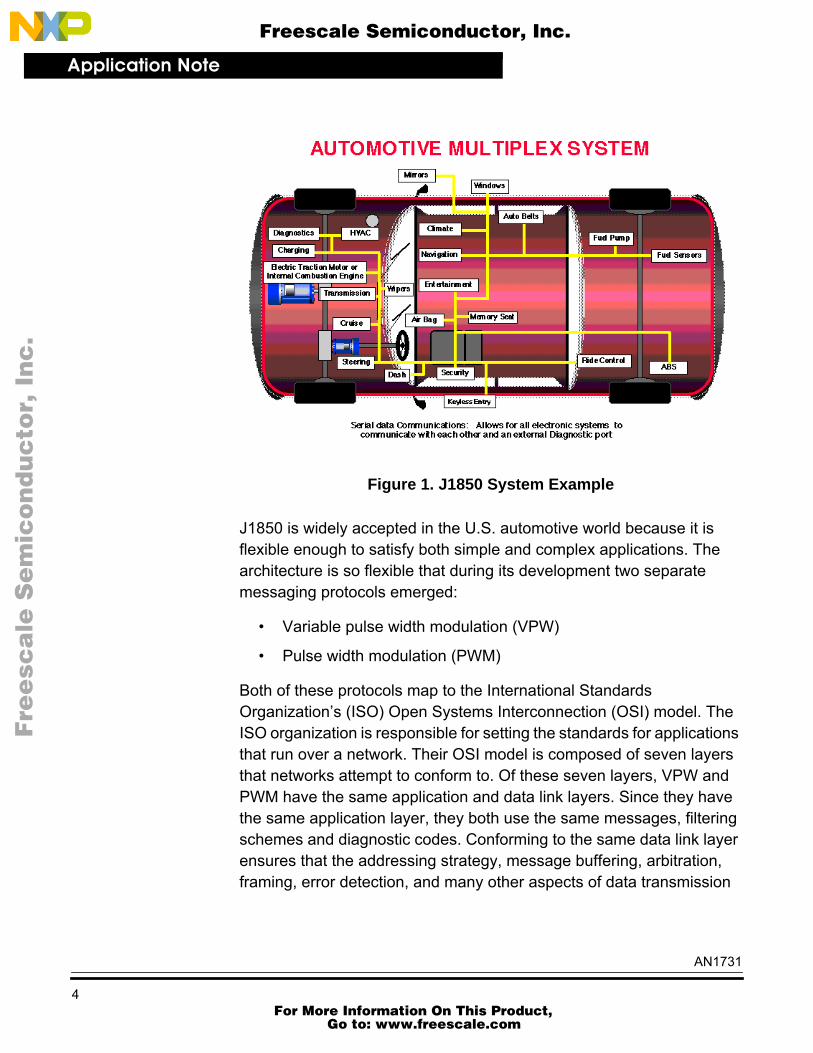
For nodes that need to communicate at medium speeds, the class B data communications network is used. To communicate at this speed, at the present time SAE has approved one bus architecture called J1850, which is an open architecture bus allowing nodes to be added or deleted easily without affecting other nodes. See Figure 1 for a diagram of the typical nodes connected to a J1850 bus.
Table 1. SAE-Approved Classes of Data Communications
Class A Class B Class C
Speed Low Medium High
Bit timings< 10 Kbits per second
(bps) 10 Kbps to 125 Kbps 125 Kbps to 1+ Mbps
Application Comfort systems Non-critical systems Human-critical systems
AN1731
3 For More Information On This Product,
Go to: www.freescale.com
Application Note
Fre
esc
ale
Se
mic
on
du
cto
r, I
Freescale Semiconductor, Inc.n
c..
.
Figure 1. J1850 System Example
J1850 is widely accepted in the U.S. automotive world because it is flexible enough to satisfy both simple and complex applications. The architecture is so flexible that during its development two separate messaging protocols emerged:
• Variable pulse width modulation (VPW)
• Pulse width modulation (PWM)
Both of these protocols map to the International Standards Organization’s (ISO) Open Systems Interconnection (OSI) model. The ISO organization is responsible for setting the standards for applications that run over a network. Their OSI model is composed of seven layers that networks attempt to conform to. Of these seven layers, VPW and PWM have the same application and data link layers. Since they have the same application layer, they both use the same messages, filtering schemes and diagnostic codes. Conforming to the same data link layer ensures that the addressing strategy, message buffering, arbitration, framing, error detection, and many other aspects of data transmission
AN1731
4 For More Information On This Product,
Go to: www.freescale.com
Application NoteVPW J1850
Fre
esc
ale
Se
mic
on
du
cto
r, I
Freescale Semiconductor, Inc.n
c..
.
are handled the same. (See the SAE J1850 specification for more information on the application and data link layers.)
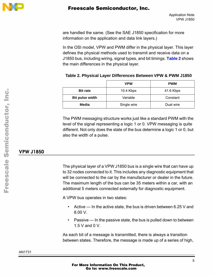
In the OSI model, VPW and PWM differ in the physical layer. This layer defines the physical methods used to transmit and receive data on a J1850 bus, including wiring, signal types, and bit timings. Table 2 shows the main differences in the physical layer.
The PWM messaging structure works just like a standard PWM with the level of the signal representing a logic 1 or 0. VPW messaging is quite different. Not only does the state of the bus determine a logic 1 or 0, but also the width of a pulse.
VPW J1850
The physical layer of a VPW J1850 bus is a single wire that can have up to 32 nodes connected to it. This includes any diagnostic equipment that will be connected to the car by the manufacturer or dealer in the future. The maximum length of the bus can be 35 meters within a car, with an additional 5 meters connected externally for diagnostic equipment.
A VPW bus operates in two states:
• Active — In the active state, the bus is driven between 6.25 V and 8.00 V.
• Passive — In the passive state, the bus is pulled down to between 1.5 V and 0 V.
As each bit of a message is transmitted, there is always a transition between states. Therefore, the message is made up of a series of high,
Table 2. Physical Layer Differences Between VPW & PWM J1850
VPW PWM
Bit rate 10.4 Kbps 41.6 Kbps
Bit pulse width Variable Constant
Media Single wire Dual wire
AN1731
5 For More Information On This Product,
Go to: www.freescale.com
Application Note
Fre
esc
ale
Se
mic
on
du
cto
r, I
Freescale Semiconductor, Inc.n
c..
.
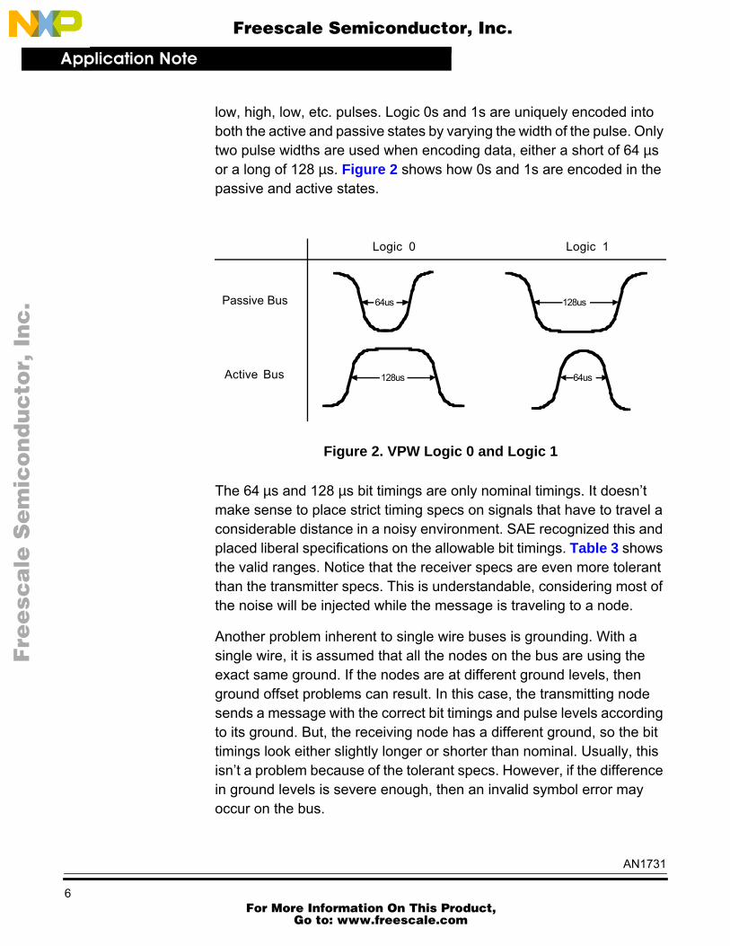
low, high, low, etc. pulses. Logic 0s and 1s are uniquely encoded into both the active and passive states by varying the width of the pulse. Only two pulse widths are used when encoding data, either a short of 64 µs or a long of 128 µs. Figure 2 shows how 0s and 1s are encoded in the passive and active states.
Figure 2. VPW Logic 0 and Logic 1
The 64 µs and 128 µs bit timings are only nominal timings. It doesn’t make sense to place strict timing specs on signals that have to travel a considerable distance in a noisy environment. SAE recognized this and placed liberal specifications on the allowable bit timings. Table 3 shows the valid ranges. Notice that the receiver specs are even more tolerant than the transmitter specs. This is understandable, considering most of the noise will be injected while the message is traveling to a node.
Another problem inherent to single wire buses is grounding. With a single wire, it is assumed that all the nodes on the bus are using the exact same ground. If the nodes are at different ground levels, then ground offset problems can result. In this case, the transmitting node sends a message with the correct bit timings and pulse levels according to its ground. But, the receiving node has a different ground, so the bit timings look either slightly longer or shorter than nominal. Usually, this isn’t a problem because of the tolerant specs. However, if the difference in ground levels is severe enough, then an invalid symbol error may occur on the bus.
Logic 0 Logic 1
Passive Bus
Active Bus
64us
64us
128us
128us
AN1731
6 For More Information On This Product,
Go to: www.freescale.com
Application NoteVPW J1850
Fre
esc
ale
Se
mic
on
du
cto
r, I
Freescale Semiconductor, Inc.n
c..
.
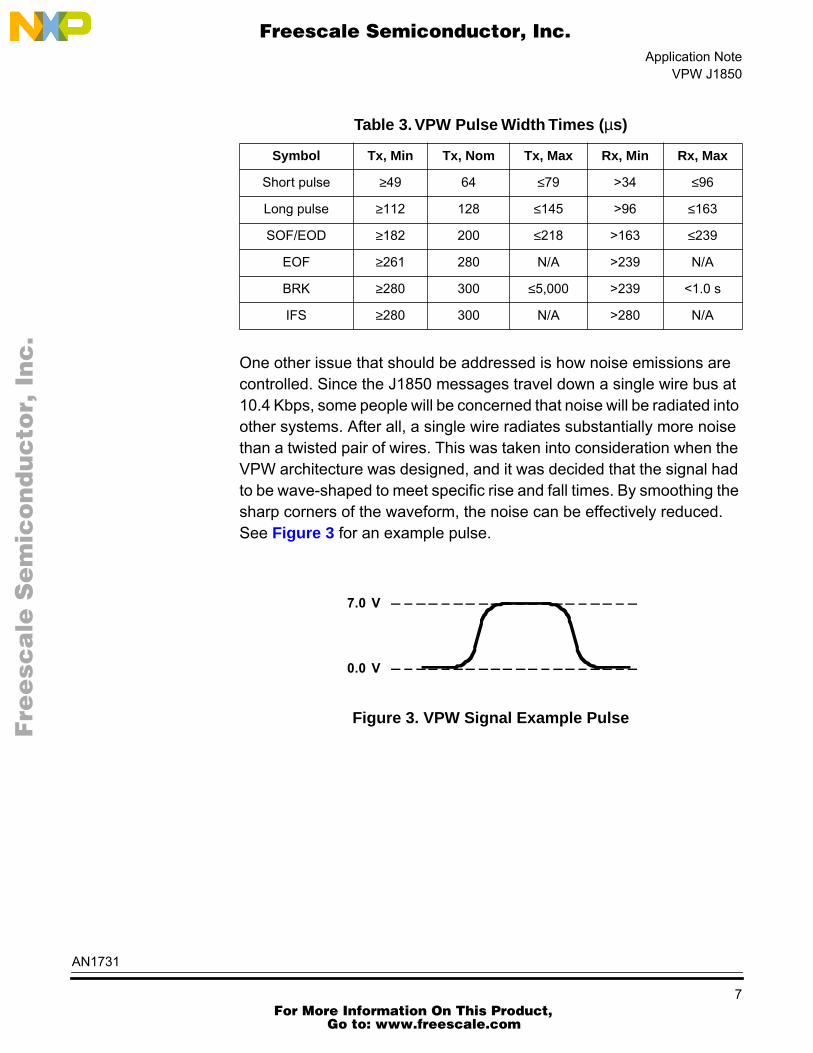
One other issue that should be addressed is how noise emissions are controlled. Since the J1850 messages travel down a single wire bus at 10.4 Kbps, some people will be concerned that noise will be radiated into other systems. After all, a single wire radiates substantially more noise than a twisted pair of wires. This was taken into consideration when the VPW architecture was designed, and it was decided that the signal had to be wave-shaped to meet specific rise and fall times. By smoothing the sharp corners of the waveform, the noise can be effectively reduced. See Figure 3 for an example pulse.
Figure 3. VPW Signal Example Pulse
Table 3. VPW Pulse Width Times (µs)
Symbol Tx, Min Tx, Nom Tx, Max Rx, Min Rx, Max
Short pulse ≥49 64 ≤79 >34 ≤96
Long pulse ≥112 128 ≤145 >96 ≤163
SOF/EOD ≥182 200 ≤218 >163 ≤239
EOF ≥261 280 N/A >239 N/A
BRK ≥280 300 ≤5,000 >239 <1.0 s
IFS ≥280 300 N/A >280 N/A
0.0 V
7.0 V
AN1731
7 For More Information On This Product,
Go to: www.freescale.com
Application Note
Fre
esc
ale
Se
mic
on
du
cto
r, I
Freescale Semiconductor, Inc.n
c..
.
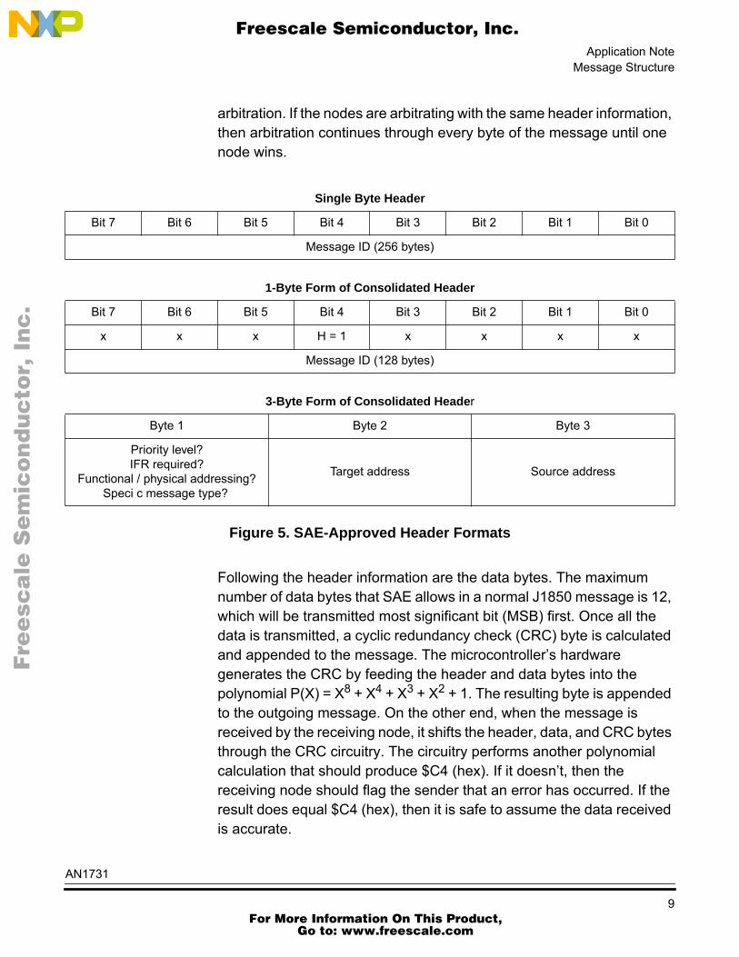
Message Structure
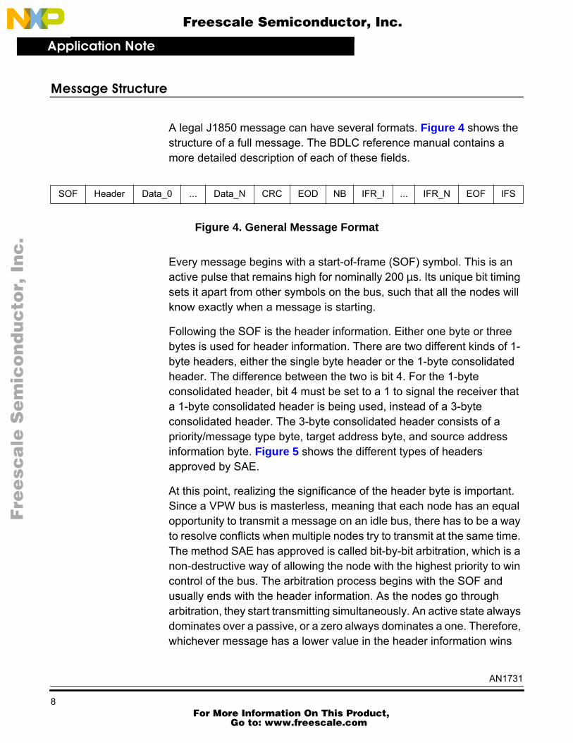
A legal J1850 message can have several formats. Figure 4 shows the structure of a full message. The BDLC reference manual contains a more detailed description of each of these fields.
Figure 4. General Message Format
Every message begins with a start-of-frame (SOF) symbol. This is an active pulse that remains high for nominally 200 µs. Its unique bit timing sets it apart from other symbols on the bus, such that all the nodes will know exactly when a message is starting.
Following the SOF is the header information. Either one byte or three bytes is used for header information. There are two different kinds of 1- byte headers, either the single byte header or the 1-byte consolidated header. The difference between the two is bit 4. For the 1-byte consolidated header, bit 4 must be set to a 1 to signal the receiver that a 1-byte consolidated header is being used, instead of a 3-byte consolidated header. The 3-byte consolidated header consists of a priority/message type byte, target address byte, and source address information byte. Figure 5 shows the different types of headers approved by SAE.
At this point, realizing the significance of the header byte is important. Since a VPW bus is masterless, meaning that each node has an equal opportunity to transmit a message on an idle bus, there has to be a way to resolve conflicts when multiple nodes try to transmit at the same time. The method SAE has approved is called bit-by-bit arbitration, which is a non-destructive way of allowing the node with the highest priority to win control of the bus. The arbitration process begins with the SOF and usually ends with the header information. As the nodes go through arbitration, they start transmitting simultaneously. An active state always dominates over a passive, or a zero always dominates a one. Therefore, whichever message has a lower value in the header information wins
SOF Header Data_0 ... Data_N CRC EOD NB IFR_I ... IFR_N EOF IFS
AN1731
8 For More Information On This Product,
Go to: www.freescale.com
Application NoteMessage Structure
Fre
esc
ale
Se
mic
on
du
cto
r, I
Freescale Semiconductor, Inc.n
c..
.
arbitration. If the nodes are arbitrating with the same header information, then arbitration continues through every byte of the message until one node wins.
Figure 5. SAE-Approved Header Formats
Following the header information are the data bytes. The maximum number of data bytes that SAE allows in a normal J1850 message is 12, which will be transmitted most significant bit (MSB) first. Once all the data is transmitted, a cyclic redundancy check (CRC) byte is calculated and appended to the message. The microcontroller’s hardware generates the CRC by feeding the header and data bytes into the polynomial P(X) = X8 + X4 + X3 + X2 + 1. The resulting byte is appended to the outgoing message. On the other end, when the message is received by the receiving node, it shifts the header, data, and CRC bytes through the CRC circuitry. The circuitry performs another polynomial calculation that should produce $C4 (hex). If it doesn’t, then the receiving node should flag the sender that an error has occurred. If the result does equal $C4 (hex), then it is safe to assume the data received is accurate.
Single Byte Header
Bit 7 Bit 6 Bit 5 Bit 4 Bit 3 Bit 2 Bit 1 Bit 0
Message ID (256 bytes)
1-Byte Form of Consolidated Header
Bit 7 Bit 6 Bit 5 Bit 4 Bit 3 Bit 2 Bit 1 Bit 0
x x x H = 1 x x x x
Message ID (128 bytes)
3-Byte Form of Consolidated Header
Byte 1 Byte 2 Byte 3
Priority level?IFR required?
Functional / physical addressing?Speci c message type?
Target address Source address
AN1731
9 For More Information On This Product,
Go to: www.freescale.com
Application Note
Fre
esc
ale
Se
mic
on
du
cto
r, I
Freescale Semiconductor, Inc.n
c..
.
Freescale has developed two modules that can communicate on an SAE J1850 10.4- Kbps VPW bus:
• Message data link controller (MDLC)
• Byte data link controller (BDLC)
These names refer to how the module handles transmitting and receiving messages on the bus, either an entire message at a time or a byte at a time. Both modules are designed to perform the critical J1850 protocol requirements automatically, such as automatic transmission synchronization to bus frame slots, calculation/auto-insertion/checking of message CRCs, and checking for symbol/framing errors.
The MDLC was the first integrated J1850 module on an 8-bit microcontroller. It is optimized for messages that require a 3-byte header, CRC, and no IFR. One transmit and two receive buffers are built into the MDLC’s hardware. Each buffer is 11 bytes long, which means that only 11 data bytes can be transmitted in a message. However, since there are two receive buffers, a message of any length can be received correctly by the module.
There are several benefits to having built-in buffers like the MDLC. For instance, it makes transmitting and receiving messages easy from a software point of view. When a transmission fails to go out due to a loss of arbitration, the hardware is designed to retransmit the message automatically once the bus is available. Again, this reduces the amount of user code needed. Aside from software savings, the MDLC also affords hardware savings because it has a built-in transceiver.
The next integrated J1850 module that was developed by Freescale is the BDLC. As the name implies, it deals with messages on a byte-by-byte basis, unlike the MDLC which handles entire messages at a time. The BDLC was intended to be a more simplistic MDLC, where the user software has more control over how the node reacts to messages on the bus. One example of this is how filtering is handled by the BDLC. Since the user’s software can evaluate each byte as it is being received, the software can determine whether to process or ignore the message. With
AN1731
10 For More Information On This Product,
Go to: www.freescale.com
Application NoteMotorola’s MDLC vs. BDLC
Fre
esc
ale
Se
mic
on
du
cto
r, I
Freescale Semiconductor, Inc.n
c..
.
this added control comes the price of needing more sophisticated software.
Another benefit of the BDLC is that it supports all the features in the J1850-VPW specification, including the optional ones, such as in-frame response. It has become a popular module and has been integrated on several families of microcontrollers, including the HC05, HC08, and HC12.
Similarities of the MDLC and the BDLC modules include:
• SAE J1850 compatible
• 10.4-Kbps variable pulse width (VPW) modulation format
• Digital noise filter
• Collision detection
• Hardware cyclical redundancy check (CRC) generation and verification
• Two power-saving modes with automatic wake up on network activity
• Polling and CPU interrupts available
• Receive block mode supported
Differences between the MDLC and the BDLC modules include:
• The MDLC cannot transmit in block mode, but the BDLC can.
• The MDLC can co-exist with devices supporting 4X mode, but it ignores all the 4X messages. The BDLC can receive messages in 4X mode, but cannot transmit in that mode.
• The MDLC automatically will try to retransmit a message when it loses arbitration during a transmission. The BDLC will generate an interrupt when the module loses arbitration, but the user’s software must take care of retransmitting the message.
• The MDLC does not support in-frame response (IFR). The BDLC supports IFR types 0, 1, 2, and 3.
AN1731
11 For More Information On This Product,
Go to: www.freescale.com
Application Note
Fre
esc
ale
Se
mic
on
du
cto
r, I
Freescale Semiconductor, Inc.n
c..
.
• The MDLC has a built-in transceiver, whereas an external transceiver must be provided for the BDLC for most parts. The BDLC modules that do not have built-in transceivers have analog and digital loopback modes for debugging the transceiver.
A Closer Look at BDLC
For an in-depth description of the BDLC module, use the Byte Data Link Controller Reference Manual. It provides information about the BDLC for any HC05, HC08, and HC12 microcontroller. This section of the application note explains some of the less intuitive features of the BDLC, including:
• How the BDLC is enabled
• When receiver and transmitter circuitry is activated following a reset
• What flags are set in the BDLC state vector register (BSVR) as a result of an error
• How an EOF flag can wake a part from wait mode
• How the digital loopback mode works with stop mode
How the BDLC is Enabled
The BDLC does not have an enable bit like Motorola’s SPI (serial peripheral interface) and SCI (serial communications interface) communications modules on microcontrollers. Instead, it is automatically enabled during any type of microcontroller reset.
When Receiver and Transmitter Circuitry is ActivatedAfter a Reset
The first thing the BDLC does following a reset is wait until it observes an idle bus for ~280 µs or an EOF time period. When it sees this, it enables the receiver circuitry and sets the EOF flag in the BSVR. At this point, the BDLC is ready to receive messages, but first the EOF flag should be cleared by the user’s software.
The only situation where the EOF flag will not be set after a reset is if the ignore message bit (IMSG) in BDLC control register 1 (BCR1) is set at
AN1731
12 For More Information On This Product,
Go to: www.freescale.com
Application NoteA Closer Look at BDLC
Fre
esc
ale
Se
mic
on
du
cto
r, I
Freescale Semiconductor, Inc.n
c..
.
the end of the 280-µs startup period. With IMSG bit set, all the BDLC interrupt requests are masked and the status bits in the BSVR are held in their reset state. Even with the EOF flag not being set, the receiver circuitry is still activated.
NOTE: It is recommended that the IMSG bit in BCR1 not be cleared by the user’s software. The BDLC hardware automatically clears this bit when receiving a message, re-enabling the BDLC interrupts. The IMSG bit should be set only when the user has determined that the incoming message is of no interest.
Similarly, the BDLC won’t activate the transmitter circuitry until it observes a passive period of 20 µs on the bus or an inter-frame separator (IFS) time period. Since there isn’t an IFS flag in the BSVR, this enable sequence is transparent to the user.
What Flags are Set in the BSVR as a Result of an Error
The BDLC has two error flags:
• CRC error flag
• Invalid symbol or out-of-range error flag
A CRC error occurs when the BDLC shifts an incoming message through its CRC error checking circuitry and the result is not correct. When this happens, the BDLC handles the error like this:
• While the data bytes are being received, the RDRF flag gets set as usual.
• When the erroneous CRC is received, first the RDRF flag is set because the CRC byte is received.
• Then the CRC error flag is set, because the result of the CRC polynomial calculation was not correct. This does not stop the reception of the rest of the message, so the EOD, NB, IFR, EOF, and IFS symbols are received as normal.
• At the end of the message an EOF flag will be set, just like it would be for a good message. At this point, the message is completely received, and the user’s code should deal with the bad message appropriately.
AN1731
13 For More Information On This Product,
Go to: www.freescale.com
Application Note
Fre
esc
ale
Se
mic
on
du
cto
r, I
Freescale Semiconductor, Inc.n
c..
.
• Once all the flags are cleared, the BDLC is ready to continue transmitting and receiving messages.
The invalid symbol or out-of-range error flag is handled slightly differently than the CRC error. This error flag encompasses all errors on the bus outside of the CRC error. Therefore, the user will not be able to determine exactly what caused the invalid symbol error. For this reason, the BDLC will stop transmitting a byte immediately if an error occurs during transmission and will set the invalid symbol flag. Likewise, if the BDLC receives a bad byte, it immediately will discard the incoming byte and set the invalid symbol flag. In this case, the BDLC waits until the bus is idle for an EOF time period (~280 µs) before receiving any new messages. The BDLC will signal that an EOF time period has expired by setting the EOF flag. After the invalid symbol and EOF flags are cleared, the BDLC is ready to continue communicating on the J1850 bus.
How an EOF Flag Can Wake a Part from Wait Mode
If the part is in wait mode with the internal clocks running, an EOF flag will wake it up. Under most circumstances, this won’t happen because the EOF flag is generated only after a message is received, a reset, or an invalid symbol.
NOTE: Be careful to execute the WAIT instruction after the EOF interrupt after a reset or an invalid symbol.
How the Digital Loopback Mode Works with Stop Mode
When the digital loopback mode bit (DLOOP) is set in the BDLC control register 2 (BCR2), the transmit and receive pins are tied together internally. This works fine for all scenarios except one: when using digital loopback, stop mode, and an external transceiver that inverts the polarity of the receive pin. When using a transceiver that inverts the receive signal, most users clear the receive pin polarity bit (RXPOL) in the BDLC analog and roundtrip delay register (BARD). That way the receive pin is inverted back to normal orientation internally by the microcontroller.
If the STOP instruction is executed with the above hardware and software set up, then the transmit pin will idle low when not transmitting and the receive pin will see a high. This is because of the internal inverter on the receive pin and the DLOOP is set. When the STOP instruction is
AN1731
14 For More Information On This Product,
Go to: www.freescale.com
Application NoteBDLC Example Software Program
F
ree
sca
le S
em
ico
nd
uc
tor,
I
Freescale Semiconductor, Inc.n
c..
.
executed with the two opposite polarities on the pins, the BDLC will interpret this as activity on the bus and immediately wake up the part.
The best way to work around this scenario is to put an inverter integrated circuit between the transceiver’s RX pin and the microcontroller’s BDRxD pin and set the RXPOL bit in the BARD to normal/true polarity.
BDLC Example Software Program
Refer to the BDLC reference manual for generic flowcharts on initializing the BDLC, transmitting messages, receiving messages, and transmitting IFRs.
The program GEN_BDLC in Appendix A shows one of the many ways of writing drivers for the BDLC. Its purpose is to demonstrate the main functionality of the BDLC module, including transmitting a message, receiving messages, filtering incoming messages, and dealing with loss of arbitration and various errors. It points out the correct sequence that should be used to program the module and any idiosyncrasies that the user may run into with the BDLC.
The comments in the program explain in detail how it works, but here’s a brief description of what it does.
• Immediately after a reset, the message $55 $55 $55 $55 is loaded into a RAM buffer and is transmitted on the J1850 bus. That's the only transmission that the program performs, but it can be modified easily by loading the RAM buffer with another message and transmitting it.
• As far as receiving messages, the program is designed to receive any message that contains a $55 in the second byte. It will filter out any message that doesn’t meet this requirement. If the message $6c $55 $01 $04 is received, then the module will switch into 4X receive mode and start receiving messages at 41.6 Kbps.
The most important part of the program is how the BDLC interrupts are handled. For the HC08 Family of microcontrollers, a jump table is used to service the interrupts.
AN1731
15 For More Information On This Product,
Go to: www.freescale.com
Application Note
F
ree
sca
le S
em
ico
nd
uc
tor,
I
Freescale Semiconductor, Inc.n
c..
.
NOTE: It is strongly recommended that interrupts are used with the BDLC with a jump table to ensure that data isn’t lost.
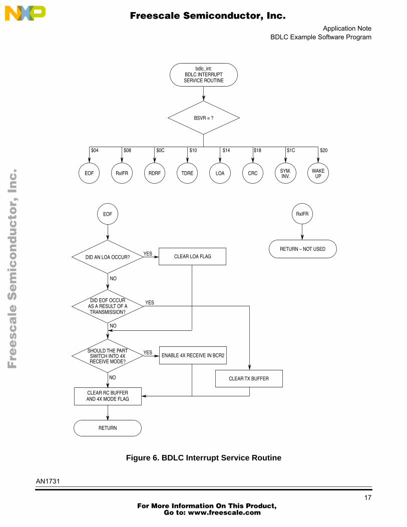
Figure 6 shows the flowchart of what happens when a BDLC interrupt occurs.
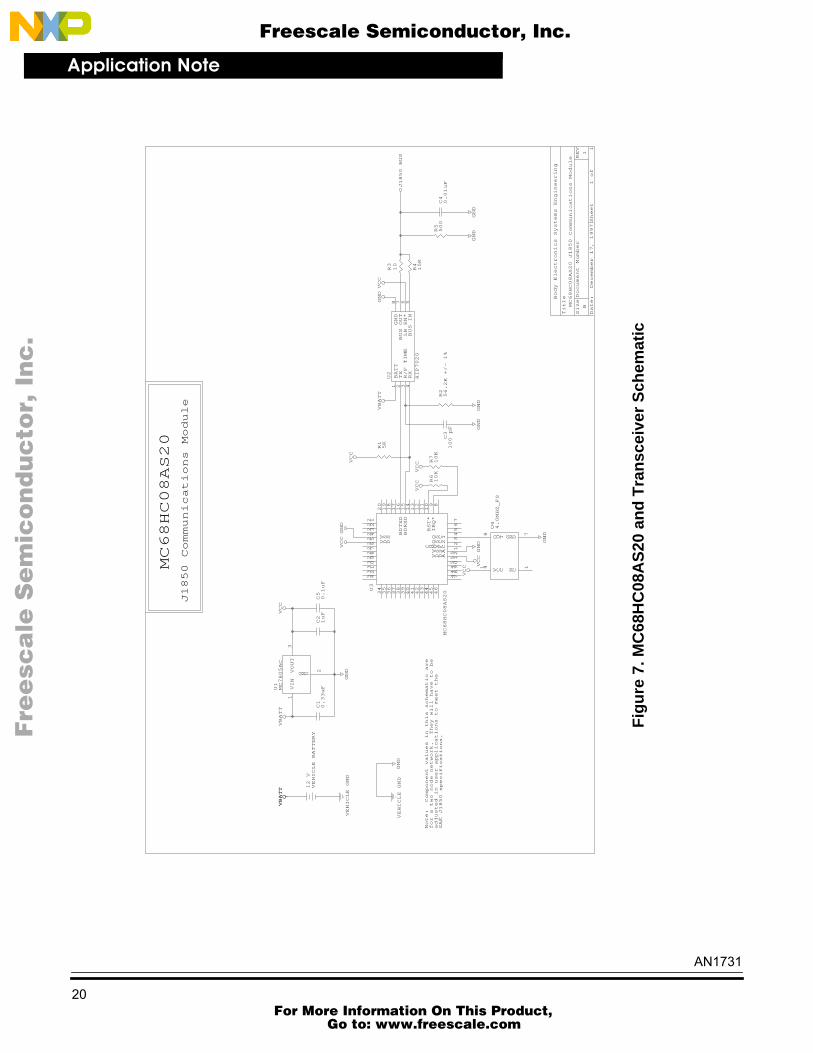
Figure 7 shows the schematic for the hardware set up.
AN1731
16 For More Information On This Product,
Go to: www.freescale.com
Application NoteBDLC Example Software Program
F
ree
sca
le S
em
ico
nd
uc
tor,
I
Freescale Semiconductor, Inc.n
c..
.
Figure 6. BDLC Interrupt Service Routine
EOF RxIFR RDRF TDRE LOA CRC SYM. WAKE
EOF
INV. UP
$04 $08 $0C $10 $14 $18 $1C $20
bdlc_int:BDLC INTERRUPTSERVICE ROUTINE
BSVR = ?
RETURN Ð NOT USED
RxIFR
SHOULD THE PARTSWITCH INTO 4XRECEIVE MODE?
DID AN LOA OCCUR?
DID EOF OCCURAS A RESULT OF ATRANSMISSION?
CLEAR RC BUFFERAND 4X MODE FLAG
RETURN
CLEAR LOA FLAG
YES
YES
NO
NO
NO
YES ENABLE 4X RECEIVE IN BCR2
CLEAR TX BUFFER
AN1731
17 For More Information On This Product,
Go to: www.freescale.com
Application Note
F
ree
sca
le S
em
ico
nd
uc
tor,
I
Freescale Semiconductor, Inc.n
c..
.
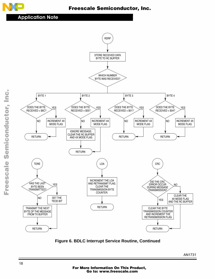
Figure 6. BDLC Interrupt Service Routine, Continued
STORE RECEIVED DATABYTE TO RC BUFFER
WHICH NUMBER
RDRF
YES
BYTE WAS RECEIVED?
DOES THE BYTERECEIVED = $6C?
BYTE 1 BYTE 2 BYTE 3 BYTE 4
INCREMENT 4XMODE FLAG
RETURN
NO
YESDOES THE BYTERECEIVED = $04?
INCREMENT 4XMODE FLAG
RETURN
NO
YESDOES THE BYTERECEIVED = $01?
INCREMENT 4XMODE FLAG
RETURN
NO
YESDOES THE BYTERECEIVED = $55?
INCREMENT 4XMODE FLAG
RETURN
NO
IGNORE MESSAGE;CLEAR THE RC BUFFER
AND 4X MODE FLAG
TDRE
YESHAS THE LASTBYTE BEEN
SET THETEOD BIT
RETURN
NO
TRANSMIT THE NEXTBYTE OF THE MESSAGE
FROM TX BUFFER
TRANSMITTED?
AND THE RC BUFFER
CRC
NODID THE CRC
ERROR OCCUR
CLEAR THE4X MODE FLAG
RETURN
YES
CLEAR THE BYTETRANSMISSION COUNTER
AND INCREMENT THE
DURING MESSAGETRANSMISSION?
RETRANSMISSION FLAG
LOA
RETURN
INCREMENT THE LOAAND RETRANSMIT FLAG.
CLEAR THETRANSMISSION BYTE
COUNTER.
AN1731
18 For More Information On This Product,
Go to: www.freescale.com
Application NoteBDLC Example Software Program
F
ree
sca
le S
em
ico
nd
uc
tor,
I
Freescale Semiconductor, Inc.n
c..
.
Figure 6. BDLC Interrupt Service Routine, Continued
SYM.
RETURN Ð NOT USED
WAKE
DID THE CRC ERROR
DELAY FOR AN EOFTIME PERIOD
RETURN
CLEAR THE 4X MODE FLAGYES
NO
CLEAR THE BYTE
UPINV.
OCCUR DURING MESSAGETRANSMISSION?
AND THE RC BUFFER
TRANSMISSION COUNTERAND INCREMENT
THE RETRANSMISSIONFLAG
AN1731
19 For More Information On This Product,
Go to: www.freescale.com
Application Note
F
ree
sca
le S
em
ico
nd
uc
tor,
I
Freescale Semiconductor, Inc.n
c..
.
Date:December 17, 1997Sheet
1
of
1
SizeDocument Number
REV
B1
Title
MC68HC08AS20 J1850 Communications Module
Body Electronics Systems Engineering
J1850 Communications Module
MC68HC08AS20
12 V
VEHICLE BATTERY
C1
0.33uF
VBATT
VOUT
3
VIN
1
G N D
2
U1
MC7805AC
VEHICLE GND
VBATT
VBATT
VCC
C2
1uFVCC
GND
C5
0.1uF
GND
VCC
VCC
J1850 BUS
GND
GND
GND
C40.01uF
R310
R415K
R5500
GND
GND
VBATT
R1
5K
VCC
VCC
BATT
1
TX
2
R/F TIME
3
RX
4
GND
8
BUS OUT
7
LB EN*
6
BUS IN
5
U2
HIP7020
R6
10K
R7
10K
R2
56.2K +/- 1%
C3
100 pF
VCC
GND
VCC
34
35
36
37
38
39
40
41
42
43
44
45
46
4 74 84 95 05 1V D D A
5 2V S S A
1C G M X F C
2O S C 2
3O S C 1
4567
8
IRQ*
9
RST*
10
11
12
13
14
BDRXD
15
BDTXD
16
17
18
19
20
2 12 2
2 3
V S S
2 4
V D D
2 52 6
2 72 8
2 93 0
3 13 2
3 4U3
MC68HC08AS20
Note: Component values in this schematic are
for a two node network. They will have to be
SAE J1850 specifications.
adjusted in user applications to meet the
GND
VEHICLE GND
GND
N C
1
V C C
1 4
O U T
8
G N D
7
U4
4.0MHZ_FS
Fig
ure
7. M
C68
HC
08A
S20
an
d T
ran
scei
ver
Sch
emat
ic
AN1731
20 For More Information On This Product,
Go to: www.freescale.com
Application NoteGeneral BDLC Driver Routines for J1850 Communication
F
ree
sca
le S
em
ico
nd
uc
tor,
I
Freescale Semiconductor, Inc.n
c..
.
General BDLC Driver Routines for J1850 Communication
******************************************************************************************************************************************************* ** General BDLC Driver Routines for J1850 Communication ** ***************************************************************************** ** File Name: gen_bdlc.asm Copyright (c) 1997 ** ** Current Revision: 1.0 ** Current Release Level: RP ** Current Revision Release Date: 2/18/98 ** ** Current Release Written By: Kim Sparks ** Freescale Systems Engineering - Austin, TX ** ** Assembled Under: CASM08 (P&E Micro Inc.) Ver.: 3.06 SLD ** ** Project Folder Name: GEN_BDLC ** ** ** Part Family Software Routine Works With: HC08 ** Part Module(s) Software Routine Works With: bdlc_d20 ** bdc_a20 ** ** Routine Size (Bytes): 312 ** RAM Used (Bytes): 30 ** ** Full Functional Description Of Routine Design: ** ** This program demonstrates the main functionality of the BDLC module, ** including transmitting a message, receiving messages, filtering ** incoming messages, dealing with loss of arbitration and various errors. ** It points out the correct procedures for programming the module and ** any idiosyncrasies with the BDLC module. ** ** Immediately following a reset the message $55 $55 $55 $55 is loaded ** into a ram buffer and transmitted on the J1850 bus. The format of the ** message being transmitted consists of a three byte consolidated header ** followed by one data byte. In real-life user applications, the messages ** used for J1850 communication will contain more data bytes and possibly ** a different header format. The one transmission following a reset is ** the only transmission that the program performs. This can be easily ** modified by loading the RAM buffer with another message and initiating ** a transmission. ** ** As far as receiving messages, the program is designed to receive only *
AN1731
21 For More Information On This Product,
Go to: www.freescale.com
Application Note
*
F
ree
sca
le S
em
ico
nd
uc
tor,
I
Freescale Semiconductor, Inc.n
c..
.
* messages that contain a $55 in the second byte. The program will ** filter out messages that don't meet this criteria. If the message ** $6c $55 $01 $04 is received, then the module will switch into 4x ** receive mode and start receiving messages at 41.6 Kbps. ** ** This program was developed for the 68HC908AS20 and 68HC908AT60, but it ** will work with any HC08 that has the BDLC ver. bdlc_d20 or greater. ** The other hardware used in the application was a 4.0 MHz canned ** oscillator to clock the AS20 and a HIP7020 transceiver to waveshape the ** the J1850 messages. ** ***************************************************************************** ** Freescale reserves the right to make changes without further notice to ** any product herein to improve reliability, function, or design. Freescale** does not assume any liability arising out of the application or use of ** any product, circuit, or software described herein; neither does it ** convey any license under its patent rights nor the rights of others. ** Freescale products are not designed, intended, or authorized for use as ** components in systems intended for surgical implant into the body, or ** other applications intended to support life, or for any other ** application in which the failure of the Freescale product could create a ** situation where personal injury or death may occur. Should Buyer ** purchase or use Freescale products for any such intended or unauthorized ** application, Buyer shall indemnify and hold Freescale and its officers, ** employees, subsidiaries, affiliates, and distributors harmless against ** all claims, costs, damages, and expenses, and reasonable attorney fees ** arising out of, directly or indirectly, any claim of personal injury or ** death associated with such unintended or unauthorized use, even if such ** manufacture of the part. Freescale claim alleges that Freescale was ** negligent regarding the design or and the Freesca;e Logo are registered ** trademarks of Freescale Semiconductor Inc. * ********************************************************************************* Equates ********************************************************************************
*** BDLC Register Equates ***
bard equ $3b ;BDLC analog and roundtrip delaybcr1 equ $3c ;BDLC control register 1bcr2 equ $3d ;BDLC control register 2bsvr equ $3e ;BDLC state vector registerbdr equ $3f ;BDLC data register
*** BARD Bit Assignments ***
ate equ 7 ;Analog transceiver enable bitrxpol equ 6 ;Receive pin polarity bitbo3 equ 3 ;Bard offset bit 3bo2 equ 2 ;Bard offset bit 2
AN1731
22 For More Information On This Product,
Go to: www.freescale.com
Application NoteGeneral BDLC Driver Routines for J1850 Communication
F
ree
sca
le S
em
ico
nd
uc
tor,
I
Freescale Semiconductor, Inc.n
c..
.
bo1 equ 1 ;Bard offset bit 1bo0 equ 0 ;Bard offset bit 0
*** BCR1 Bit Assignments ***
imsg equ 7 ;Ignore message bitclks equ 6 ;Clock bitr1 equ 5 ;Rate select bit 1r0 equ 4 ;Rate select bit 0test1 equ 3 ;Mode pins when using an MMDStest0 equ 2 ; dev. sys with EM boardie equ 1 ;Interrupt enable bitwcm equ 0 ;Wait clock mode bit
*** BCR2 Bit Assignments ***
aloop equ 7 ;Analog loopback mode bitdloop equ 6 ;Digital loopback mode bitrx4xe equ 5 ;Receive 4x enable bitnbfs equ 4 ;Normalization bit format select bitteod equ 3 ;Transmit end of data bittsifr equ 2 ;Transmit single byte IFR with no CRC bittmifr1 equ 1 ;Transmit multiple byte IFR with CRC bittmifr0 equ 0 ;Transmit multiple byte IFR without CRC bit
*** BDLC Interrupt Sources ***
eof equ $04 ;Received an end of framerxifr equ $08 ;Received IFR byterdrf equ $0c ;BDLC Rx data register fulltdre equ $10 ;BDLC Tx data register emptyloa equ $14 ;Loss of arbitrationcrc_err equ $18 ;Cyclical redundancy check errorinvalid equ $1c ;Symbol invalid or out of rangewake_up equ $20 ;Wakeup
*** General Equates for the MC68HC08AS20 ***
ram equ $50 ;User RAMrom equ $ae00 ;User ROMconfig equ $1f ;Configuration register
bdlc_vec equ $ffdc ;BDLC interrupt vector (high)reset equ $fffe ;Reset vector (high)
AN1731
23 For More Information On This Product,
Go to: www.freescale.com
Application Note
F
ree
sca
le S
em
ico
nd
uc
tor,
I
Freescale Semiconductor, Inc.n
c..
.
******************************************************************************** HC08 RAM Storage Assignments ********************************************************************************
org ram
*** BDLC Flags ***
retx_flag rmb $1 ;Retransmit flagrc4x_flag rmb $1 ;4x mode flagloa_flag rmb $1 ;Loss of arbitration flag
*** Transmit Message Count and Buffer ***
tdre_cnt rmb $1 ;Total number of bytes that have been ; transmittedtx_message rmb $d ;Transmit buffer, first byte is the # of ; bytes in the message to transmit & the ; remaining bytes make up the message
*** Receive Message Count and Buffer ***
rc_message rmb $d ;Receive buffer, first byte is the # of ; bytes received & remaining bytes are ; the message
******************************************************************************** Main Program ********************************************************************************
**************************************************************************** Following a reset the BDLC and MCU are initialized, and the transmit* routine is called. Once the first byte of the message is loaded into the* the BDR the program stays in a loop that checks to see if the message* needs to be retransmitted.***************************************************************************
org romstart: mov #$03,config ;Enable the stop instruction & disable ; the COP jsr bdlc_init ;Initialize the BDLC module jsr mcu_init ;Initialize the MCU
retran: jsr transmit ;Transmit a message
clra ;Check for loss of arbitration or CRChere: cbeq retx_flag,here ; error, retransmit the message if set clr retx_flag ;Reset the error flag bra retran ;Branch back to the where the transmit ; routine is called
AN1731
24 For More Information On This Product,
Go to: www.freescale.com
Application NoteGeneral BDLC Driver Routines for J1850 Communication
F
ree
sca
le S
em
ico
nd
uc
tor,
I
Freescale Semiconductor, Inc.n
c..
.
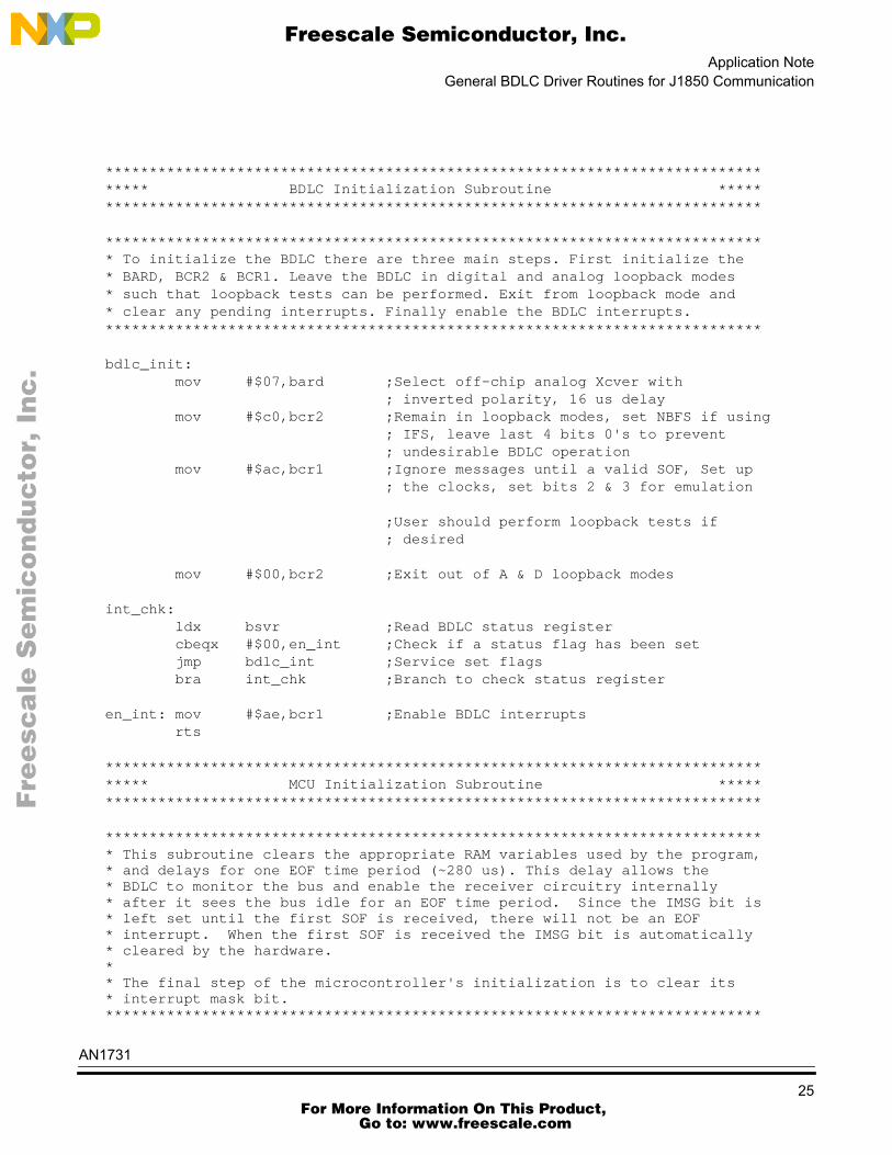
******************************************************************************** BDLC Initialization Subroutine ********************************************************************************
**************************************************************************** To initialize the BDLC there are three main steps. First initialize the* BARD, BCR2 & BCR1. Leave the BDLC in digital and analog loopback modes* such that loopback tests can be performed. Exit from loopback mode and* clear any pending interrupts. Finally enable the BDLC interrupts.***************************************************************************
bdlc_init: mov #$07,bard ;Select off-chip analog Xcver with ; inverted polarity, 16 us delay mov #$c0,bcr2 ;Remain in loopback modes, set NBFS if using ; IFS, leave last 4 bits 0's to prevent ; undesirable BDLC operation mov #$ac,bcr1 ;Ignore messages until a valid SOF, Set up ; the clocks, set bits 2 & 3 for emulation
;User should perform loopback tests if ; desired
mov #$00,bcr2 ;Exit out of A & D loopback modes
int_chk: ldx bsvr ;Read BDLC status register cbeqx #$00,en_int ;Check if a status flag has been set jmp bdlc_int ;Service set flags bra int_chk ;Branch to check status register
en_int: mov #$ae,bcr1 ;Enable BDLC interrupts rts
******************************************************************************** MCU Initialization Subroutine ********************************************************************************
**************************************************************************** This subroutine clears the appropriate RAM variables used by the program,* and delays for one EOF time period (~280 us). This delay allows the* BDLC to monitor the bus and enable the receiver circuitry internally* after it sees the bus idle for an EOF time period. Since the IMSG bit is* left set until the first SOF is received, there will not be an EOF* interrupt. When the first SOF is received the IMSG bit is automatically* cleared by the hardware.** The final step of the microcontroller's initialization is to clear its* interrupt mask bit.***************************************************************************
AN1731
25 For More Information On This Product,
Go to: www.freescale.com
Application Note
F
ree
sca
le S
em
ico
nd
uc
tor,
I
Freescale Semiconductor, Inc.n
c..
.
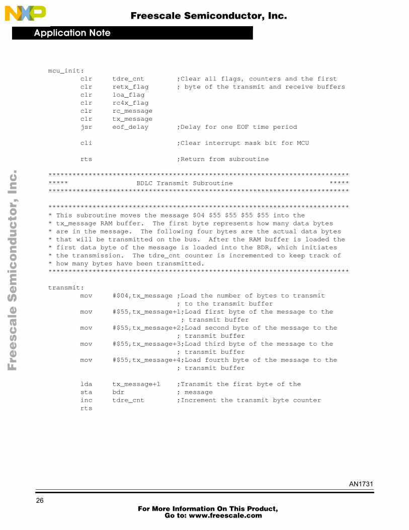
mcu_init: clr tdre_cnt ;Clear all flags, counters and the first clr retx_flag ; byte of the transmit and receive buffers clr loa_flag clr rc4x_flag clr rc_message clr tx_message jsr eof_delay ;Delay for one EOF time period
cli ;Clear interrupt mask bit for MCU
rts ;Return from subroutine
******************************************************************************** BDLC Transmit Subroutine ********************************************************************************
**************************************************************************** This subroutine moves the message $04 $55 $55 $55 $55 into the* tx_message RAM buffer. The first byte represents how many data bytes* are in the message. The following four bytes are the actual data bytes* that will be transmitted on the bus. After the RAM buffer is loaded the* first data byte of the message is loaded into the BDR, which initiates* the transmission. The tdre_cnt counter is incremented to keep track of* how many bytes have been transmitted.***************************************************************************
transmit: mov #$04,tx_message ;Load the number of bytes to transmit ; to the transmit buffer mov #$55,tx_message+1;Load first byte of the message to the ; transmit buffer mov #$55,tx_message+2;Load second byte of the message to the ; transmit buffer mov #$55,tx_message+3;Load third byte of the message to the ; transmit buffer mov #$55,tx_message+4;Load fourth byte of the message to the ; transmit buffer
lda tx_message+1 ;Transmit the first byte of the sta bdr ; message inc tdre_cnt ;Increment the transmit byte counter rts
AN1731
26 For More Information On This Product,
Go to: www.freescale.com
Application NoteGeneral BDLC Driver Routines for J1850 Communication
F
ree
sca
le S
em
ico
nd
uc
tor,
I
Freescale Semiconductor, Inc.n
c..
.
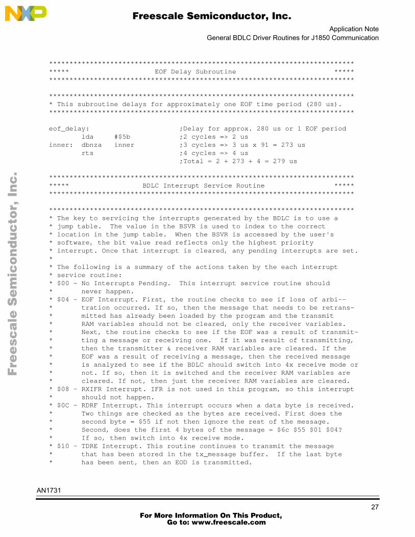
******************************************************************************** EOF Delay Subroutine ********************************************************************************
**************************************************************************** This subroutine delays for approximately one EOF time period (280 us).***************************************************************************
eof_delay: ;Delay for approx. 280 us or 1 EOF period lda #$5b ;2 cycles => 2 usinner: dbnza inner ;3 cycles => 3 us x 91 = 273 us rts ;4 cycles => 4 us ;Total = 2 + 273 + 4 = 279 us
******************************************************************************** BDLC Interrupt Service Routine ********************************************************************************
**************************************************************************** The key to servicing the interrupts generated by the BDLC is to use a* jump table. The value in the BSVR is used to index to the correct* location in the jump table. When the BSVR is accessed by the user's* software, the bit value read reflects only the highest priority* interrupt. Once that interrupt is cleared, any pending interrupts are set.** The following is a summary of the actions taken by the each interrupt* service routine:* $00 - No Interrupts Pending. This interrupt service routine should* never happen.* $04 - EOF Interrupt. First, the routine checks to see if loss of arbi--* tration occurred. If so, then the message that needs to be retrans-* mitted has already been loaded by the program and the transmit* RAM variables should not be cleared, only the receiver variables.* Next, the routine checks to see if the EOF was a result of transmit-* ting a message or receiving one. If it was result of transmitting,* then the transmitter & receiver RAM variables are cleared. If the* EOF was a result of receiving a message, then the received message* is analyzed to see if the BDLC should switch into 4x receive mode or* not. If so, then it is switched and the receiver RAM variables are* cleared. If not, then just the receiver RAM variables are cleared.* $08 - RXIFR Interrupt. IFR is not used in this program, so this interrupt* should not happen.* $0C - RDRF Interrupt. This interrupt occurs when a data byte is received.* Two things are checked as the bytes are received. First does the* second byte = $55 if not then ignore the rest of the message.* Second, does the first 4 bytes of the message = $6c $55 $01 $04?* If so, then switch into 4x receive mode.* $10 - TDRE Interrupt. This routine continues to transmit the message* that has been stored in the tx_message buffer. If the last byte* has been sent, then an EOD is transmitted.
AN1731
27 For More Information On This Product,
Go to: www.freescale.com
Application Note
F
ree
sca
le S
em
ico
nd
uc
tor,
I
Freescale Semiconductor, Inc.n
c..
.
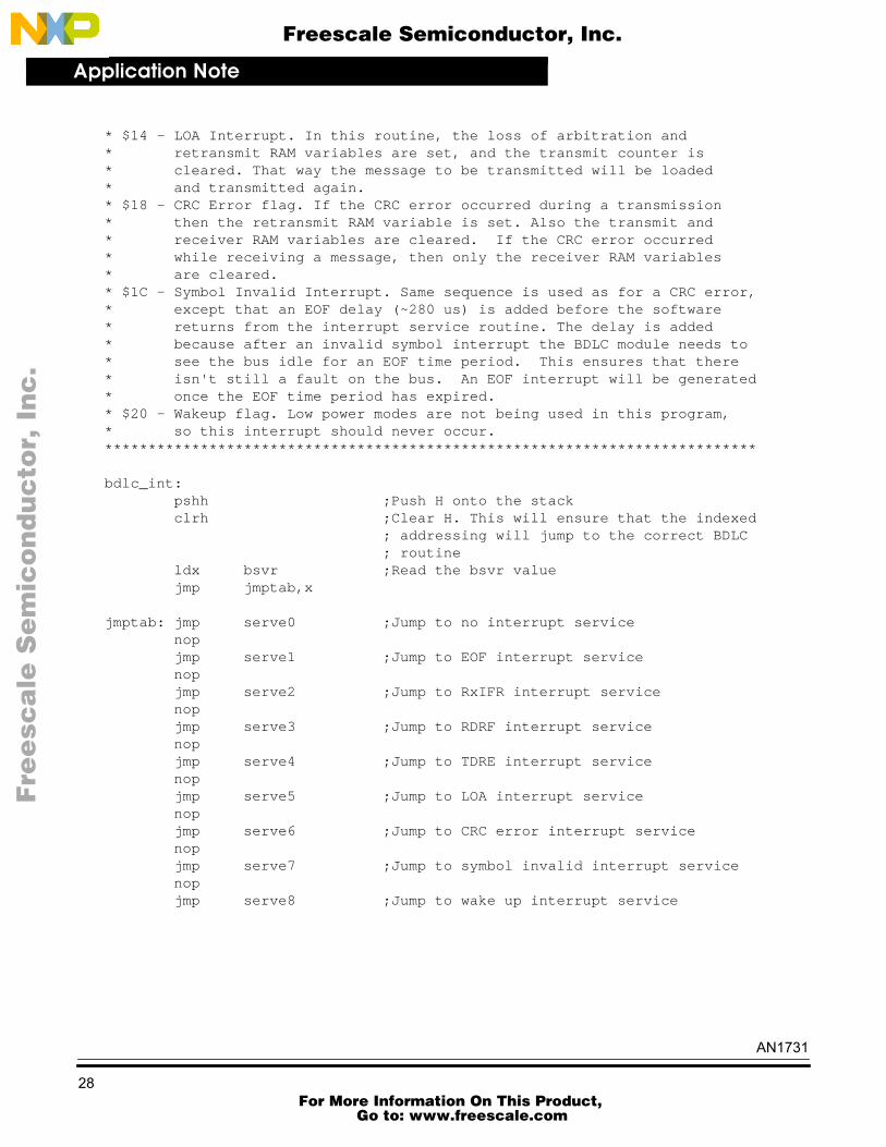
* $14 - LOA Interrupt. In this routine, the loss of arbitration and* retransmit RAM variables are set, and the transmit counter is* cleared. That way the message to be transmitted will be loaded* and transmitted again.* $18 - CRC Error flag. If the CRC error occurred during a transmission* then the retransmit RAM variable is set. Also the transmit and* receiver RAM variables are cleared. If the CRC error occurred* while receiving a message, then only the receiver RAM variables* are cleared.* $1C - Symbol Invalid Interrupt. Same sequence is used as for a CRC error,* except that an EOF delay (~280 us) is added before the software* returns from the interrupt service routine. The delay is added* because after an invalid symbol interrupt the BDLC module needs to* see the bus idle for an EOF time period. This ensures that there* isn't still a fault on the bus. An EOF interrupt will be generated* once the EOF time period has expired.* $20 - Wakeup flag. Low power modes are not being used in this program,* so this interrupt should never occur.***************************************************************************
bdlc_int: pshh ;Push H onto the stack clrh ;Clear H. This will ensure that the indexed ; addressing will jump to the correct BDLC ; routine ldx bsvr ;Read the bsvr value jmp jmptab,x
jmptab: jmp serve0 ;Jump to no interrupt service nop jmp serve1 ;Jump to EOF interrupt service nop jmp serve2 ;Jump to RxIFR interrupt service nop jmp serve3 ;Jump to RDRF interrupt service nop jmp serve4 ;Jump to TDRE interrupt service nop jmp serve5 ;Jump to LOA interrupt service nop jmp serve6 ;Jump to CRC error interrupt service nop jmp serve7 ;Jump to symbol invalid interrupt service nop jmp serve8 ;Jump to wake up interrupt service
AN1731
28 For More Information On This Product,
Go to: www.freescale.com
Application NoteGeneral BDLC Driver Routines for J1850 Communication
F
ree
sca
le S
em
ico
nd
uc
tor,
I
Freescale Semiconductor, Inc.n
c..
.
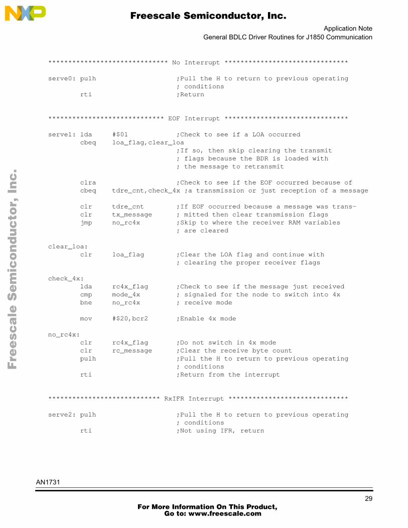
****************************** No Interrupt *******************************
serve0: pulh ;Pull the H to return to previous operating ; conditions rti ;Return
***************************** EOF Interrupt *******************************
serve1: lda #$01 ;Check to see if a LOA occurred cbeq loa_flag,clear_loa ;If so, then skip clearing the transmit ; flags because the BDR is loaded with ; the message to retransmit
clra ;Check to see if the EOF occurred because of cbeq tdre_cnt,check_4x ;a transmission or just reception of a message
clr tdre_cnt ;If EOF occurred because a message was trans- clr tx_message ; mitted then clear transmission flags jmp no_rc4x ;Skip to where the receiver RAM variables ; are cleared
clear_loa: clr loa_flag ;Clear the LOA flag and continue with ; clearing the proper receiver flags
check_4x: lda rc4x_flag ;Check to see if the message just received cmp mode_4x ; signaled for the node to switch into 4x bne no_rc4x ; receive mode
mov #$20,bcr2 ;Enable 4x mode
no_rc4x: clr rc4x_flag ;Do not switch in 4x mode clr rc_message ;Clear the receive byte count pulh ;Pull the H to return to previous operating ; conditions rti ;Return from the interrupt
**************************** RxIFR Interrupt ******************************
serve2: pulh ;Pull the H to return to previous operating ; conditions rti ;Not using IFR, return
AN1731
29 For More Information On This Product,
Go to: www.freescale.com
Application Note
F
ree
sca
le S
em
ico
nd
uc
tor,
I
Freescale Semiconductor, Inc.n
c..
.
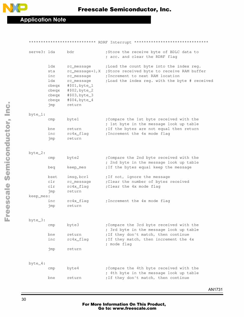
**************************** RDRF Interrupt *******************************
serve3: lda bdr ;Store the receive byte of BDLC data to ; acc. and clear the RDRF flag
ldx rc_message ;Load the count byte into the index reg. sta rc_message+1,X ;Store received byte to receive RAM buffer inc rc_message ;Increment to next RAM location ldx rc_message ;Load the index reg. with the byte # received cbeqx #$01,byte_1 cbeqx #$02,byte_2 cbeqx #$03,byte_3 cbeqx #$04,byte_4 jmp return
byte_1: cmp byte1 ;Compare the 1st byte received with the ; 1st byte in the message look up table bne return ;If the bytes are not equal then return inc rc4x_flag ;Increment the 4x mode flag jmp return
byte_2: cmp byte2 ;Compare the 2nd byte received with the ; 2nd byte in the message look up table beq keep_mes ;If the bytes equal keep the message
bset imsg,bcr1 ;If not, ignore the message clr rc_message ;Clear the number of bytes received clr rc4x_flag ;Clear the 4x mode flag jmp returnkeep_mes: inc rc4x_flag ;Increment the 4x mode flag jmp return
byte_3: cmp byte3 ;Compare the 3rd byte received with the ; 3rd byte in the message look up table bne return ;If they don't match, then continue inc rc4x_flag ;If they match, then increment the 4x ; mode flag jmp return
byte_4: cmp byte4 ;Compare the 4th byte received with the ; 4th byte in the message look up table bne return ;If they don't match, then continue
AN1731
30 For More Information On This Product,
Go to: www.freescale.com
Application NoteGeneral BDLC Driver Routines for J1850 Communication
F
ree
sca
le S
em
ico
nd
uc
tor,
I
Freescale Semiconductor, Inc.n
c..
.
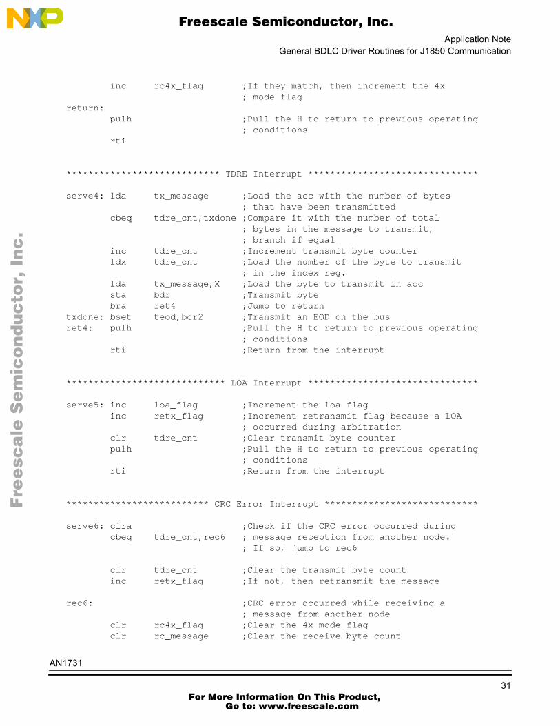
inc rc4x_flag ;If they match, then increment the 4x ; mode flagreturn: pulh ;Pull the H to return to previous operating ; conditions rti
**************************** TDRE Interrupt *******************************
serve4: lda tx_message ;Load the acc with the number of bytes ; that have been transmitted cbeq tdre_cnt,txdone ;Compare it with the number of total ; bytes in the message to transmit, ; branch if equal inc tdre_cnt ;Increment transmit byte counter ldx tdre_cnt ;Load the number of the byte to transmit ; in the index reg. lda tx_message,X ;Load the byte to transmit in acc sta bdr ;Transmit byte bra ret4 ;Jump to returntxdone: bset teod,bcr2 ;Transmit an EOD on the busret4: pulh ;Pull the H to return to previous operating ; conditions rti ;Return from the interrupt
***************************** LOA Interrupt *******************************
serve5: inc loa_flag ;Increment the loa flag inc retx_flag ;Increment retransmit flag because a LOA ; occurred during arbitration clr tdre_cnt ;Clear transmit byte counter pulh ;Pull the H to return to previous operating ; conditions rti ;Return from the interrupt
************************** CRC Error Interrupt ****************************
serve6: clra ;Check if the CRC error occurred during cbeq tdre_cnt,rec6 ; message reception from another node. ; If so, jump to rec6
clr tdre_cnt ;Clear the transmit byte count inc retx_flag ;If not, then retransmit the message
rec6: ;CRC error occurred while receiving a ; message from another node clr rc4x_flag ;Clear the 4x mode flag clr rc_message ;Clear the receive byte count
AN1731
31 For More Information On This Product,
Go to: www.freescale.com
Application Note
F
ree
sca
le S
em
ico
nd
uc
tor,
I
Freescale Semiconductor, Inc.n
c..
.
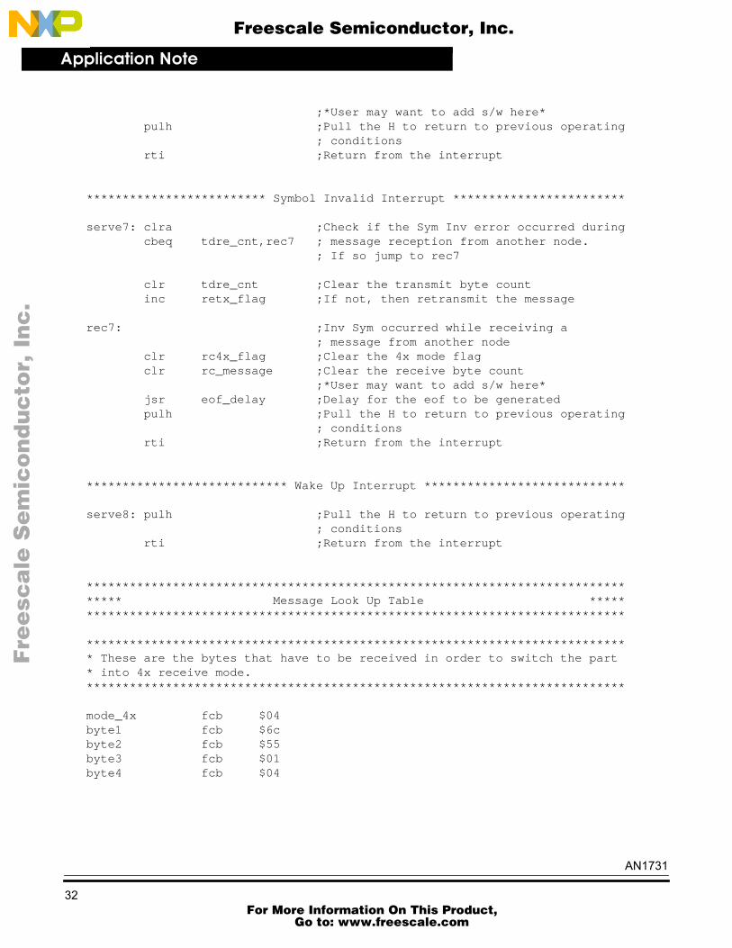
;*User may want to add s/w here* pulh ;Pull the H to return to previous operating ; conditions rti ;Return from the interrupt
************************* Symbol Invalid Interrupt ************************
serve7: clra ;Check if the Sym Inv error occurred during cbeq tdre_cnt,rec7 ; message reception from another node. ; If so jump to rec7
clr tdre_cnt ;Clear the transmit byte count inc retx_flag ;If not, then retransmit the message
rec7: ;Inv Sym occurred while receiving a ; message from another node clr rc4x_flag ;Clear the 4x mode flag clr rc_message ;Clear the receive byte count ;*User may want to add s/w here* jsr eof_delay ;Delay for the eof to be generated pulh ;Pull the H to return to previous operating ; conditions rti ;Return from the interrupt
**************************** Wake Up Interrupt ****************************
serve8: pulh ;Pull the H to return to previous operating ; conditions rti ;Return from the interrupt
******************************************************************************** Message Look Up Table ********************************************************************************
**************************************************************************** These are the bytes that have to be received in order to switch the part* into 4x receive mode.***************************************************************************
mode_4x fcb $04byte1 fcb $6cbyte2 fcb $55byte3 fcb $01byte4 fcb $04
AN1731
32 For More Information On This Product,
Go to: www.freescale.com
Application NoteGeneral BDLC Driver Routines for J1850 Communication
F
ree
sca
le S
em
ico
nd
uc
tor,
I
Freescale Semiconductor, Inc.n
c..
.
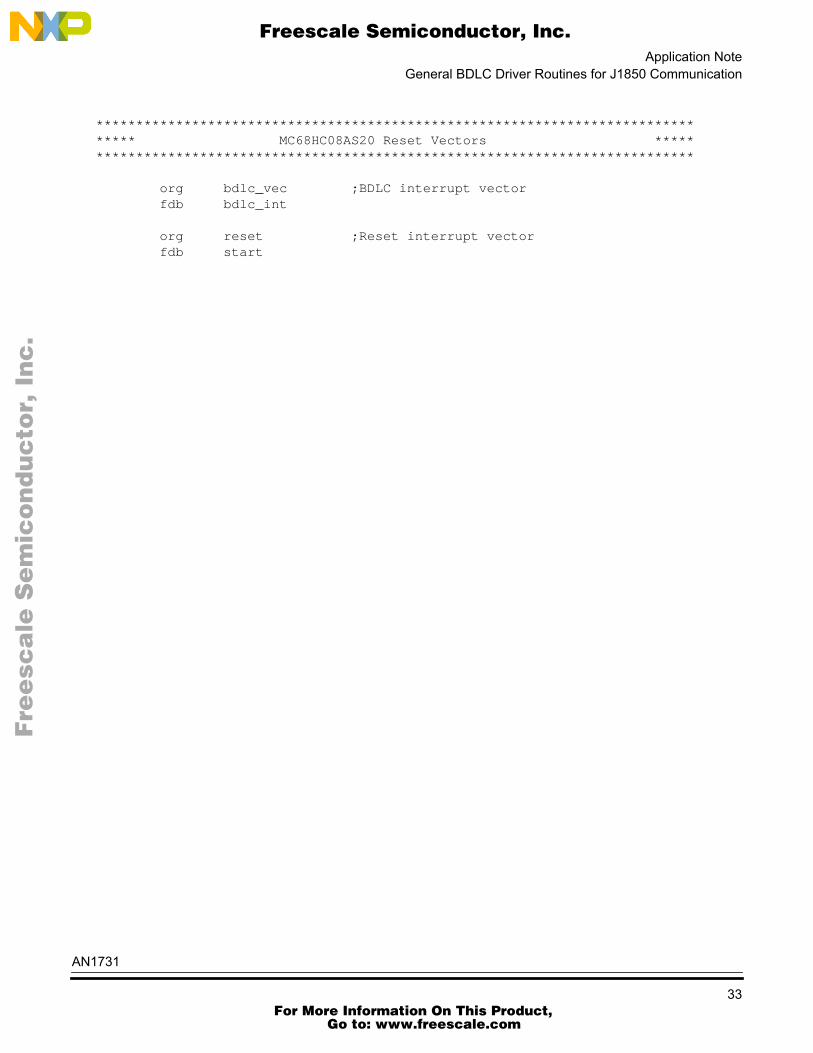
******************************************************************************** MC68HC08AS20 Reset Vectors ********************************************************************************
org bdlc_vec ;BDLC interrupt vector fdb bdlc_int
org reset ;Reset interrupt vector fdb start
AN1731
33 For More Information On This Product,
Go to: www.freescale.com

Application Note
F
ree
sca
le S
em
ico
nd
uc
tor,
I
Freescale Semiconductor, Inc.n
c..
.
AN1731
34 For More Information On This Product,
Go to: www.freescale.com
Application NoteGeneral BDLC Driver Routines for J1850 Communication
F
ree
sca
le S
em
ico
nd
uc
tor,
I
Freescale Semiconductor, Inc.n
c..
.
AN1731
35 For More Information On This Product,
Go to: www.freescale.com
N
ON
-D
IS
CL
OS
UR
E
AG
RE
EM
EN
T
RE
QU
IR
ED
Application Note
F
ree
sca
le S
em
ico
nd
uc
tor,
I
Freescale Semiconductor, Inc.n
c..
.
For More Information On This Product, Go to: www.freescale.com