voltage controlled low pass filter analog design · voltage controlled low pass filter analog...
TRANSCRIPT
Voltage Controlled Low Pass Filter Analog Design
Camilo Tejeiro and Moise Nistrian
University of Washington – Seattle, Department of Electrical Engineering, Seattle, WA, 98195
Abstract— The purpose of this lab was to design a low pass filter, which is a frequency selective circuit that passes to the output input signals that reside in a low frequency band, called the pass-band, and attenuates the effects of high frequency input signals that reside in the “stop-band”. An array of specs had to be met including a maximum ripple of 2dB in the filter pass-band of the Bode magnitude plot, a minimum attenuation of 60dB at two times the corner/cutoff frequency which is defined as the frequency at which the gain is attenuated by 3dB (also referred to as the -3dB frequency) and finally tunable from 15 kHz to 30kHz. All of the specs were met and exceeded with the implementation of a voltage controlled 12th order Butterworth filter utilizing OTA’s in the form of t he LM13700 Integrated Circuit.
Voltage Controlled Filters;gm-c filters; Analog Filters; Low pass filter
I. INTRODUCTION
The field of filter design has always been of great interest by both industry and academia. More sophisticated filters have become more widely used as the available frequencies in the electromagnetic spectrum have become more limited due to the exponential increase in the amount of data transmitted over the air. It is clear that this trend will continue but for this to be possible filtering schemes will need to increase their performance approaching the ideal brick wall model thus allowing for more signals to be transmitted using the same bandwidth. The purpose of this project was to design a high order, minimal ripple, voltage controlled filter via the use of Operational Transconductance Amplifiers and off the bench components. Future endeavors will focus on a reduction in both power consumption and the overall size factor.
II. BODY
For this design we aimed at finding a component that will lend itself to modulation of its intrinsic characteristics via the use of an external factor. After extensive research on the advantages and drawbacks of multiple types of components used to realize voltage controlled filters the team decided to narrow the list down to two types of components: transconductance amplifiers and switched capacitor circuits. Literature on switched capacitor circuits is extensive and is a field of profound research in itself, however the group’s members understanding of switched capacitors was not deep at that time and so our research on this area was suspended. On the other hand transconductance amplifiers are discussed at the start of most entry level analog design classes and the intuition behind them is very clear, further the literature found ranged from tools for understanding the very basics to more involved higher order designs that built on the basic building blocks. It has to be noted that while a good performance was achieved that exceeded the project requirements, the group could not focus on circuit efficiency, power consumption or small scale integration due to the stringent performance requirements and the very tight deadlines.
A. Design Considerations
Pass Band Ripple: As stated in the requirements the maximum ripple allowed in the pass band for this project was 2 dB, this implied that we needed a maximally flat filter response in the stop band. To achieve this we could have used a series of low Q (Q = 0.707) second order low pass cascaded filters but as will be noted later this would have imposed an unrealizable size to the order of our circuit due to the sharp roll off that needed to be achieved, we decided to use a different approach as will be described below
Sharp Roll off: One of the purposes of this project was to explore the difficulties reached as one gets closer to approximate a brick wall response, the roll off of this filter was set to be 60 dB at 2*Fc or more commonly described as (~200db/decade), this very sharp roll off is what finally ruled out our attempted implementation of cascading equal component stages with Q = 0.707. By doing this we would have achieved the ripple measure satisfactorily but the roll off would have been far from ideal and the gains from adding extra stages would have been detriment.
Tunable Cutoff: Our decision to use operational transconductance amplifiers for this design was tailored toward fulfilling this requirement, the idea was to control all OTA’s open loop gain (gm) via the use of a common biasing current, this common modulation of all the stages was visualized as a simple manner of moving the poles of all the cascaded stages at the same rate. The flexibility granted by the use of these components was a crucial factor that allowed us to make up for very large tolerances in the capacitors used which were accommodated by varying the currents of each second order stage individually to reach the desired cutoff frequencies.
Filter Approximation: Extensive research and multiple failed attempts taught us that cascading equal component stages with equal Q’s was simply not going to meet the required expectations. We needed a filter approximation that could lead us to attain maximally flat pass band response but that could be cascaded to achieve the required attenuation. The first approximations looked into were both the 0.1dB and the 1 dB Chebyschev approximations but it soon became obvious that due to the high Q’s needed for some of the stages small deviations in passive component values would have made the suppression of these peaks by the low Q stages hard to achieve and would have required a lot of tweaking at the end. We decided to pursue a Butterworth approximation which keeps peaking considerably small for each stage and sets all the cutoff frequency to the same values, the only drawback being a higher order filter.
B. Key Design equations
The Design equations used for this circuit topology are the following (Refer to the final second order filter, Appendix B.6):
Cutoff Frequency:
= + 2 Where:
= ∗ ℎ
And h is a PVT (Process, Voltage and Temperature) dependent constant.
Therefore:
= + ∗ ∗ ℎ2 Quality Factor:
= The previous equations were arranged into iterative component equations, in the following form.
1. Choose Ra = 220Ω, R = 61.9k Ω, C1 = 100p, Q = desired quality factor and fo = center frequency, compute C2 from the rearranged Q equation. = ∗
2. Now find a value of h*Ibias that will get you close to fo
∗ ℎ = ∗ + ∗ 2
3. Tweak Rbias until the reading on the ammeter is close to I bias, find center frequency and keep iteratively changing Rbias until you have converged into fo.
C. Topology Discussion &Intuition behind the circuit
To understand how our second order building block operates it is crucial to discuss two very basic topologies widely used in most analog voltage controlled filters; these are the current controlled resistor and the adjustable pole integrator. The
current controlled resistor (Appendix B.1) can be understood via a quick experiment. Take two cases, first let Ibias be equal to 0, since:
= ∗ & = ∗ ℎ Therefore gm = 0 and Io = 0 thus we will have infinite impedance looking into the OTA or Rin = ∞. Now take the second
case, let I bias be finite and apply a step at the input Vn. Vd will go negative, gm will be finite and proportional to Ibias and Io will be negative. Therefore the OTA will be sinking current through Io in an amount proportional to Vd or Ibias thus acting like a resistor tied to ground with Vd across it and with a resistance variable by Ibias.
The second circuit is the Ideal Adjustable Pole Integrator or first order low pass filter (Appendix B.2) for this circuit let’s keep the input frequency constant and change Ibias to see what is the effect on the circuit. If Ibias is very small, gm which is dependent on Ibias will be very small and so will Io therefore with this slow flow of charge it will take the capacitor a long time to charge and if Vd is changing fast enough the OTA will not be able to charge the capacitor and Vout = 0v. Now take the second case where I bias is large, If I bias is large, gm is large and Io is large. This means that now the OTA circuit can charge and discharge the capacitor a lot faster, this means that even if Vd is changing fast the OTA integrator will be able to follow the output thus acting as a buffer. Therefore by changing the bias current we can move the poles of this low pass filter independent of the Q factor. The cascaded 2 pole low pass filter (Appendix B.3) is a cascaded integrator of the type mentioned above with the output of the whole filter fed back to the input to provide negative feedback, keep Vd within reasonable limits and provide stability, the formulas for this circuit are:
= ∗ ℎ2 & = Further improvements to this circuit were needed to keep the OTA in the linear region of operation. In the circuit
(Appendix B.4) voltage dividers at the input of each stage and in the feedback loop were used to keep Vd < 20mV as recommended in the datasheet. In circuit (Appendix B.5) a resistor biasing scheme with a common control voltage was used to control both OTA gm’s in a constant manner, finally in circuit (Appendix B.6) the circuits were modified to match that recommended in the datasheet application notes, buffering the outputs of each OTA.
III. RESULTS
The results in simulation using Multisim were not duplicated when the physical circuit was built. In simulation 60dB attenuation at 2fc and less than 2dB ripple in the passband was achieved using a 10th order Butterworth and setting the corner frequency of each stage to 15kHz and 30kHz given by fo = (Ra*gm)/[(R+Ra)*2pi*C] and adjusting the transconductance, gm, by changing the biasing current. We expected the quality factor to be given by Q = sqrt(C2/C1) and initially set the quality factor of each stage to the same value. When the actual circuit was built the results were not duplicated as expected so necessary changes were made. First we made the decision to follow the values given in the table for the 10th order Butterworth where the Q of each stage increases as n (the order of the system) increases. The ripple and attenuation specs were still not met. We used a potentiometer to simulate the biasing resistor which controls the biasing current and thus gm to set each individual stage to the appropriate corner frequency with a lot more control since the frequency response could be observed live in FFT mode as the pot is varied. We realized that we needed a 12th order system to meet the attenuation spec which would give a roll off of 240dB/dec.
When the 12th order system was completed and hooked up to Labview which gave more precise and informative statistics than the Oscilloscope there seemed to be a tradeoff between attenuation and ripple. We decided to make the ripple maximum in the last two stages by increasing the Q values, this made the attenuation greater than 60dB at 2fc but the ripple was over 10dB, the only way to decrease the ripple was experimentally found to be via shifting the corner frequencies of the first two stages to the left (lower in frequency) by decreasing gm via decreasing Ibias (increasing Rbias). By shifting the corner frequencies of the first two stages to the left we were able to cancel out the large ripple produced by the high Q values of the last two stages. This proved to be the solution that allowed us to meet all the specs, further since the circuit’s response was
linear because the differential voltage was kept under 20 millivolts via voltage dividers at the inputs and the feedback networks therefore the filter’s response was identical at 15kHz and 30kHz.
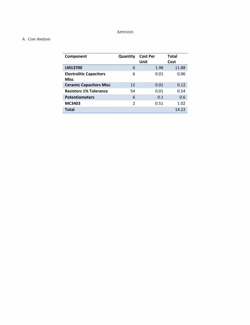
The ripple for our system in the pass-band was accurately measured to be 1.8dB, the attenuation at 2 fc was 63dB and the filter was tunable from 15 kHz to 30 kHz via a common control voltage. The parts cost measure for our circuit can be found in Appendix A and the total current consumption was measured to be 34.3 mA with +- 12V supply rails.
IV. CONCLUSION
This lab was a good introduction into low pass filter design. It quickly became evident that in order to meet specs a number of trade-offs had to be considered. A lot of attenuation had to be achieved in the stop band while achieving a small ripple voltage in the pass band therefore a number of solutions had to be explored. Our design choice of cascading six two pole voltage controlled filters using OTAs gave us a lot of control. Being able to tune the center frequencies of each individual second order stage was vital to be able to meet the ripple and attenuation specs. The biggest drawbacks of using OTAs turned out to be how different the actual system response was from that simulated in Multisim as well as some non-idealities of the OTA’s themselves (e.g. small linearity range, limited bias current range, poor power efficiency). Another hurdle that was run into was that the circuit did not lend itself very well to manual component’s tweaking due to the large number of variables involved in the overall circuit’s response. Given the previous drawbacks, it should be noted that our OTAs implementation was very effective in terms of giving us a lot of control of each second order stage via its biasing current.
REFERENCES [1] R. L. Geiger, et al., "Voltage Controlled Filter Design Using Operational Transconductance Amplifiers," IEEE,, , 1983.
Document: http://class.ece.iastate.edu/vlsi2/docs/Linked%20Publications/1983-05-ISCAS-RL.pdf [2] R.L. Geiger, et al., "Active Filter Design Using Operational Transconductance Amplifiers: A Tutorial" IEEE Circuits And Devices Magazine, Vol 1,pp
20-32, March 1985. Document: http://class.ece.iastate.edu/vlsi2/docs/Linked%20Publications/1985-03-ICADM-RG.pdf
[3] B. Hutchings,et al,"Additional Design Ideas For Voltage Controlled Filters," IEEE Circuits And Devices Magazine,,, 1985. Document: http://electronotes.netfirms.com/EN85VCF.PDF
[4] R. Marston, et al., "Understanding and Using OTA Op Amp IC’s",Part 1, 2003. Document: http://www.scribd.com/doc/104211013/Understanding-and-Using-OTA-OP-Amps-by-Ray-Marston
[5] , ,"LM13700 Datasheet Application’s Notes,",, 2004. Document: http://www.ti.com/lit/ds/symlink/lm13700.pdf
APPENDIX
A. Cost Analysis
Component Quantity Cost Per
Unit
Total
Cost
LM13700 6 1.98 11.88
Electrolitic Capacitors
Misc
6 0.01 0.06
Ceramic Capacitors Misc 12 0.01 0.12
Resistors 1% Tolerance 54 0.01 0.54
Potentiometers 6 0.1 0.6
MC3403 2 0.51 1.02
Total 14.22
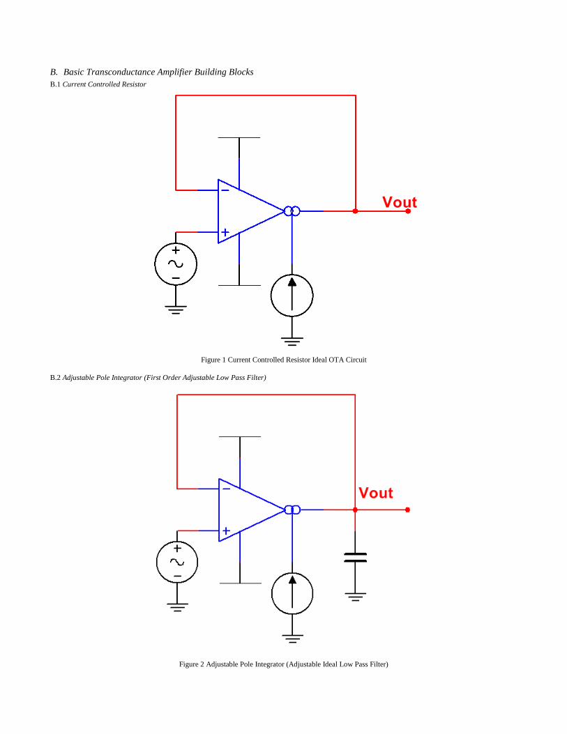
B. Basic Transconductance Amplifier Building Blocks B.1 Current Controlled Resistor
Figure 1 Current Controlled Resistor Ideal OTA Circuit
B.2 Adjustable Pole Integrator (First Order Adjustable Low Pass Filter)
Figure 2 Adjustable Pole Integrator (Adjustable Ideal Low Pass Filter)
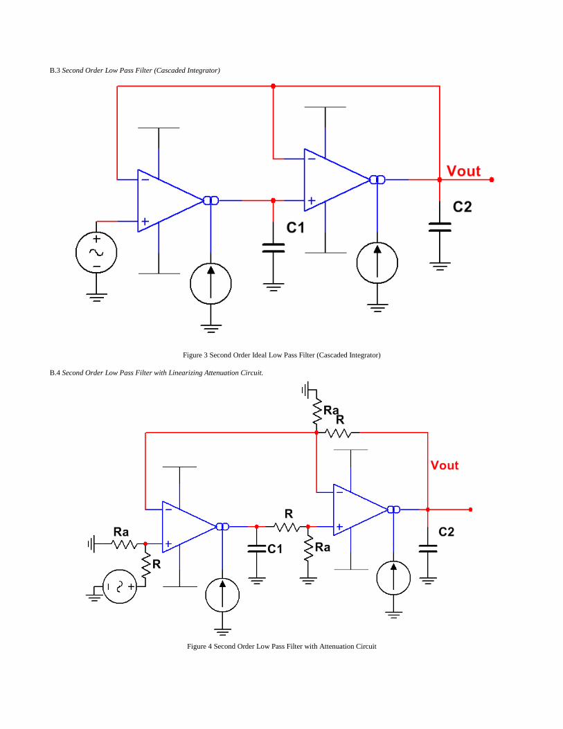
B.3 Second Order Low Pass Filter (Cascaded Integrator)
Figure 3 Second Order Ideal Low Pass Filter (Cascaded Integrator)
B.4 Second Order Low Pass Filter with Linearizing Attenuation Circuit.
Figure 4 Second Order Low Pass Filter with Attenuation Circuit
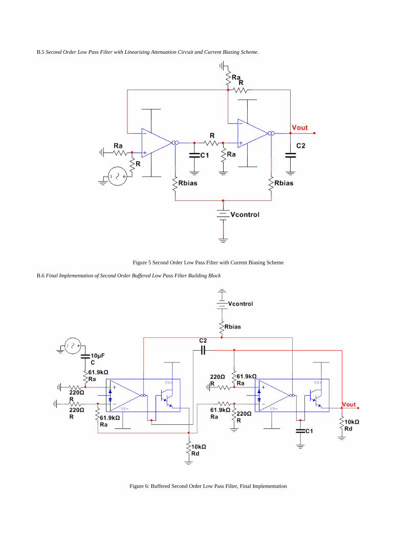
B.5 Second Order Low Pass Filter with Linearizing Attenuation Circuit and Current Biasing Scheme.
Figure 5 Second Order Low Pass Filter with Current Biasing Scheme
B.6 Final Implementation of Second Order Buffered Low Pass Filter Building Block
Figure 6: Buffered Second Order Low Pass Filter, Final Implementation
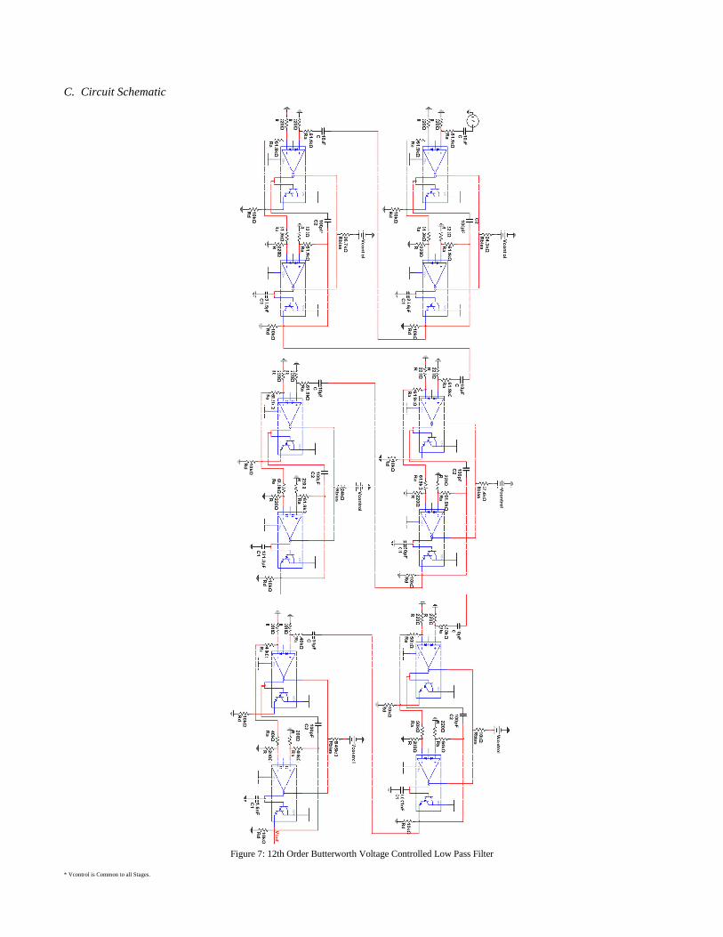
C. Circuit Schematic
Figure 7: 12th Order Butterworth Voltage Controlled Low Pass Filter
* Vcontrol is Common to all Stages.
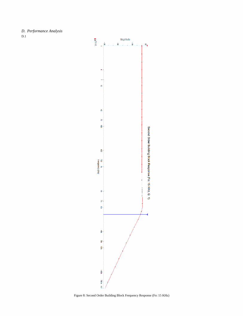
D. Performance Analysis D.1
Figure 8: Second Order Building Block Frequency Response (Fo: 15 KHz)
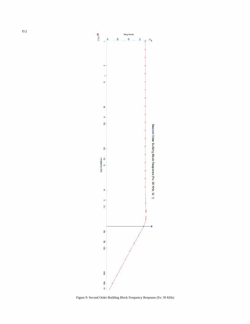
D.2
Figure 9: Second Order Building Block Frequency Response (Fo: 30 KHz)
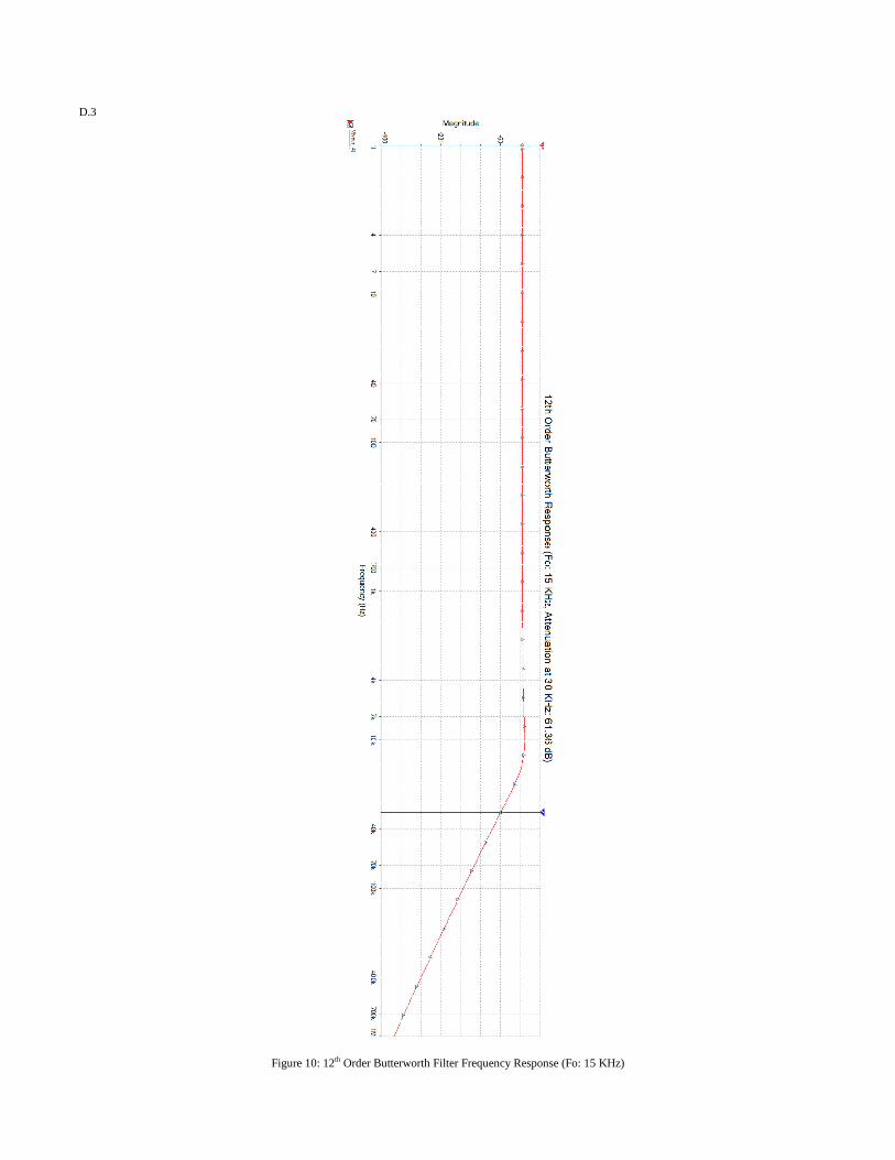
D.3
Figure 10: 12th Order Butterworth Filter Frequency Response (Fo: 15 KHz)
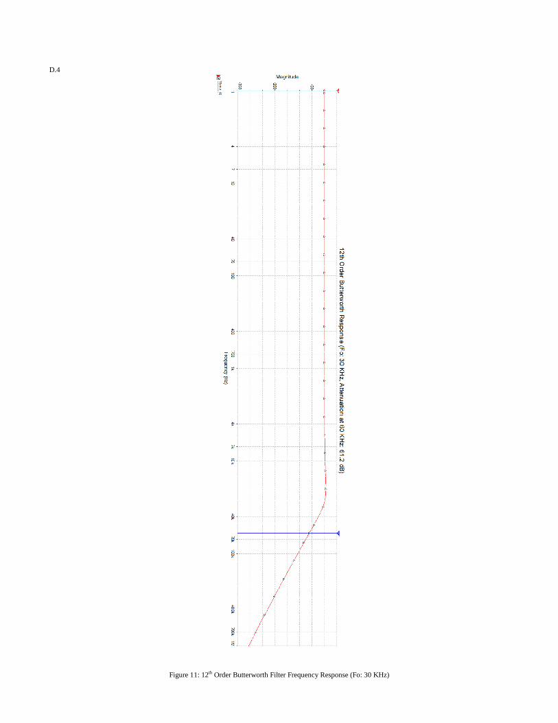
D.4
Figure 11: 12th Order Butterworth Filter Frequency Response (Fo: 30 KHz)