vhdl training report
DESCRIPTION
summer training report on vhdl.in cetpa infotech in roorkeeTRANSCRIPT
TABLE OF CONTENTS
1. INTRODUCTION
1.1 VHDL DESIGN FLOW
1.2. INITIAL DESIGN ENTRY
1.3. WHAT IS VHDL?
1.4. HISTORY
1.5. CAPABILITES OF VHDL
1.6. ADVANTAGES OF VHDL OVER PROCEDURAL LANGUAGES
2. THE VHDL DESIGN HIERARCHY
2.1. DESING ENETITY
2.2. ENTITY DECLARATION
2.3. ARCHITECTURE BODY
2.3.1 DATA FLOW STYLE
2.3.2 BEHAVIORAL STYLE
2.3.3 STRUCTURAL STYLE
3. LOGIC SYNTHESIS
3.1. LOGIC OPTIMIZATION TECHNIQUES
a)AREA OPTIMIZATION
b)SPEED OPTIMIZATION
4. FPGA
5. ALU
6 Code For 8 bit Adder-Substractor
7 Code for 8 bit Multiplier
8 Code for Final ALU
9 Future Prospects of VHDL
1. INTRODUCTION
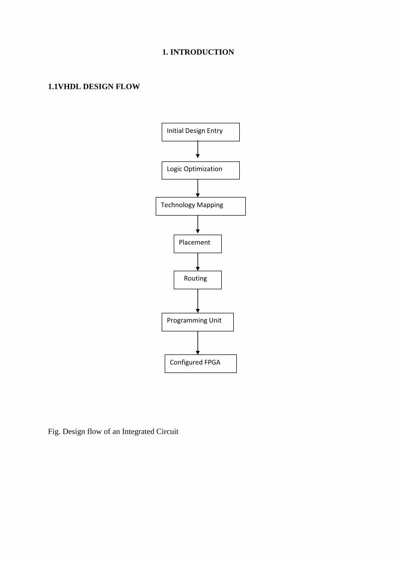
1.1VHDL DESIGN FLOW
Fig. Design flow of an Integrated Circuit
Initial Design Entry
Logic Optimization
Technology Mapping
Programming Unit
Placement
Routing
Configured FPGA
1.2. INITIAL DESIGN ENTRY
As integrated circuit technology has improved to allow more and more components on a chip,
digital systems have continued to grow in complexity. As digital systems have become more
complex, detailed design of the systems at the gate and flop-flop level has become very
tedious and time consuming. For this reason, use of hardware languages in the digital design
process continues to grow importance. A hardware description language allows a digital
system to be designed and debugged at a higher level before conversion to the gate and flip
flop level. Use of synthesis computer aided design tools to do this conversion is becoming
more widespread. This is analogous to writing software programs in high-level languages
such as C and then using a compiler to convert the programs to machine language. The two
most popular hardware description languages are VHDL and Verilog.
1.3. WHAT IS VHDL?
VHDL is an acronym for very high-speed integrated circuit hardware description language. It
is a general-purpose hardware description language that is specifically designed to describe
the organization and function of digital hardware system, circuit boards & components at
many level of abstraction ranging from simple gate to complete digital electronics systems.
VHDL model is a textual description of a hardware design or a piece of design that, when
simulated mimics the design behavior.
1.4. HISTORY
The requirement for the language were first generated in 1980, under the Very High Speed
Integrated Circuit (VHSIC) project of US government, to enhance the electronic design
process, technology, and procurement, spawning development of many advanced integrated
circuit process technologies. In this program, a number of US companies were involved in the
design of VHSIC chip for the Department of Defense (DOD), USA. At that time, most of the
companies were using different HDL to describe and developed their ICs. As a result
different vender could not effectively exchange design with one another. Thus a need for a
standardized HDL for the design, documentation and verification of digital system was
generated. A team of three of companies, IBM, TI & INTERMETRICS, developed a version
of language. In 1986, VHDL was proposed as an IEEE standard. It went through a number of
revisions and changes until it was adopted as the IEEE 1076 standard in December 1987.
1.5. CAPABILITES OF VHDL
The following are the major capabilities that VHDL provide along with the feature that
differentiate it from other Hardware Description languages.
1. The language can be used as an exchange medium between chip vender and CAD tool
users. Different chip venders can provide VHDL description of their components to system
designers. CAD tool users can use it to capture the behavior of the design at a high level of
abstraction for functional simulation.
2. The language can also be used as a communication medium between different CAD and
CAM tools. For example a schematic capture program may be used to generate a VHDL
description for the design, which can be used as an input to a simulation program.
3. The language supports hierarchy i.e. a digital system can be modeled as a set of
interconnected sub-components.
4. The language is not technology specific, but is capable of supporting different
technologies. It can support various hardware technologies: for example - new logic types
and new components may be defined; technology specific attributes can be used. By being
technology independent the same model can be synthesized into different vendor libraries.
5. It supports both synchronous and asynchronous timing models.
6. It is an IEEE and ANSI STANDARD; therefore, models described in this language are
portable.
7. The language supports three basic different description styles: structural, data flow and
behavioral. A design may be described in any combination of these three descriptive styles.
8. It supports a wide range of abstraction level ranging from behavioral description to very
precise gate level descriptions. It does not however support modeling at or below the
transistor level. It allows a design to be captured at a mixed level using a single coherent
language.
9. Arbitrary large design can be modeled using the language, and there are no limitations
imposed by the language on the size of a design.
10. The language has element that make large-scale modeling easier, for example component,
functions, procedure, and packages.
11. Nominal propagation delays, min-max delay, setup and holding time and spike detection
can all be very naturally done in this language.
12. A model can, not only describe the functionality of a design but also the information
about the design itself in terms of user defined attributes such as total area and speed.
13. A common language can be used to describe library components from different vendors.
Tools that understand VHDL models will have no difficulty in reading models from a variety
of venders since the languages is a standard.
14. Models written in this language can be verified by simulation, since precise simulation
semantics are defined for language construct.
15. The capability of defining new data types provides the power of describe and simulate a
new design technique at a very high level of abstraction without any concern the
implementation details.
16.The language is publicly available and human readable.
1.6. ADVANTAGES OF VHDL OVER PROCEDURAL LANGUAGES
Main difference between VHDL and other programming languages like C/C++ are
a) VHDL is a parallel language, while C/C++ are sequential languages. Each statement
occurring in VHDL is executed concurrently, while in C/C++ each statement is executed
sequentially and at its own turn. In VHDL explicit constructs exist for explicit sequential
steps.
b) VHDL is a strongly typed language. It doesn’t allow any mismatching of types, though
type conversion is permitted.
c) VHDL allows use of explicit time delay, which isn’t applicable in procedural languages. In
procedural languages the right hand side value is assigned to the left hand side value as soon
as the statement is executed. In VHDL there is an advantage that the computed value can be
assigned to a signal after any time delay.
d) VHDL model cannot be implemented in real time application directly like other procedural
languages. It is simulated and synthesized using in built system clock.
2. THE VHDL DESIGN HIERARCHY
Any hardware design can be described in terms of its operation at different levels of
abstraction, from system through to logic gate. At each level of this hierarchy the overall
inputs and outputs remain the same but the functionality of distinct sections become clearer.
When the local inputs and outputs and the function of a block are sufficiently defined, the
hardware can be designed.
VHDL is capable of describing a well-defined hardware block at any level of
abstraction. A design entity is the VHDL representation of such a block and can be
considered to be at the top of the design hierarchy. Within the design entity, the function of
the hardware is often further decomposed by using external and internal blocks.
External blocks are other design entities that have been previously complied and
stored in a library. These types of blocks are generally referred to as components. Each
component can further extend the hierarchy by also using external and internal blocks to
describe its own function. The present design entity can also be thought of as external block.
Internal blocks are self-contained functional units that have explicitly defined input
and output signals. They therefore represent the next level down in the hierarchy. Again, an
internal block may contain external or other internal blocks. The Block statement is used to
create an internal block.
A design entity contains an entity declaration and an architecture body. Figure below shows
the organization of the VHDL design hierarchy and illustrates the main elements of an
architecture body. The port connection, enable information to be passed between blocks and,
at the top level, allow the design entity to communicate with the external environment. A
design entity may contain any or all of the elements shown, in the diagram. It will always
have an entity declaration and architecture body at the top level
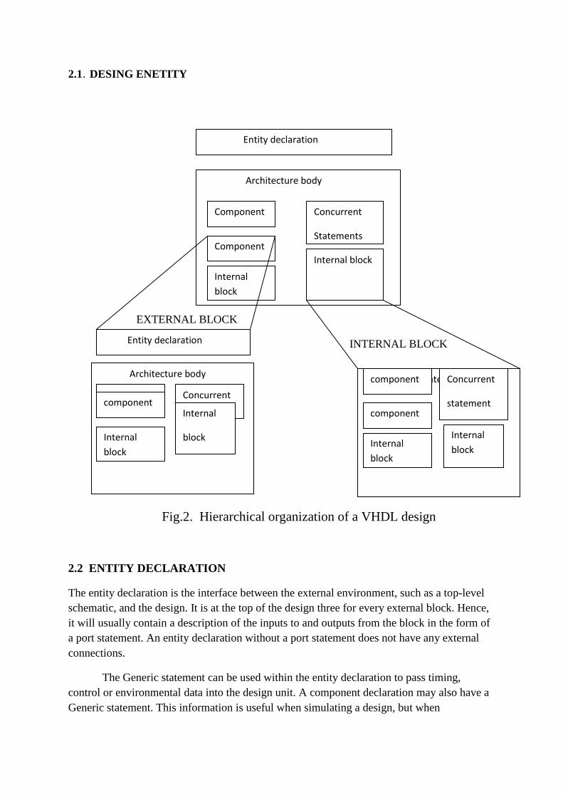
2.1. DESING ENETITY
EXTERNAL BLOCK
INTERNAL BLOCK
Fig.2. Hierarchical organization of a VHDL design
2.2 ENTITY DECLARATION
The entity declaration is the interface between the external environment, such as a top-level
schematic, and the design. It is at the top of the design three for every external block. Hence,
it will usually contain a description of the inputs to and outputs from the block in the form of
a port statement. An entity declaration without a port statement does not have any external
connections.
The Generic statement can be used within the entity declaration to pass timing,
control or environmental data into the design unit. A component declaration may also have a
Generic statement. This information is useful when simulating a design, but when
Entity declaration
Architecture body
Component Concurrent
Statements Component
Internal block
Internal
block
Architecture body
Entity declaration
component Concurrent
statements
component
Internal
block
Internal
block
Block statement component
component
Concurrent
statement
Internal
block
Internal
block
synthesizing most of it is irrelevant. Hence, the Generic statement usually only supports the
declaration of integer generics, which have a constant value and can therefore be substituted
into the associated design unit at compile time.
The syntax for entity declaration is as follows
Entity entity – name is
[port (interface-signal-declaration);]
end [entity] [entity-name];
2.3. ARCHITECTURE BODY
The architecture body is used to specify the relationship between the inputs and outputs
declared in the entity. It therefore describes the actual function of the hardware. Although
each entity must be unique, several architectures can be associated with one entity. This
allows the function of a block to the changed without changing its external structure.
The architecture body contains any number of concurrent statements components and
internal blocks are also of this type. These statements can be considered to be executing
asynchronously and completely independently of each other. It is therefore crucial to
understand how the relationships between different concurrent statements are going to affect
not only the behavior but also the logical structure of the hardware that synthesis will
produce.
Additionally, certain concurrent statements may contain a number of sequentially
executing statements. Such flexibility allows the architecture body to be constructed using
three possible language styles. Choosing a particular approach does not limit the design to
that one style. In fact, many functional descriptions can be implemented in more than one
style. In general, a combination of two or all three styles is often required to obtain the most
compact and clear VHDL code.
2.3.1 Dataflow style
Dataflow style architecture models the hardware in terms of the movement of data Over
continuous time between combinational logic components such as adders, decoders and
primitive logic gates. It describes the register-transfer level behavior of a circuit. The
language topics that are most relevant to the dataflow style of architecture include the
following:
Operators-logical, relational and mathematical;
Operator overloading;
Concurrent assignment statements.
This style is not appropriate for the modeling of sequential logic. Instead, and as its name
suggests, it is best applied in the modeling of data driven elements such as an arithmetic logic
unit (ALU)
2.3.2 Behavioral style
The behavioral style architecture contains concurrent statements with sections of sequential
statements that describe the outputs of the circuit at a discrete moment in time given
particular inputs. While similar language constructs are often found in dataflow and
behavioral style architectures, only the latter explicitly exhibit the notions of time and
control. This style describes the function of the circuit at the algorithmic level.
The aspects of VHDL that are most relevant to behavioral style architectures include the
following
-Process statements and sensitivity lists;
-Sequential statements;
-Variables.
This architectural style is used to describe both sequential and combinational circuits. Hence,
it is a valuable design approach for finite state machines (FSMs) or any control logic.
2.3.3. Structural style
A structural style architecture describes the circuit primarily in terms of components. These
may be drawn from libraries supplied by ASIC vendors, modules that are purposely produced
for this design or general, user defined modules that are stored in a library created for a
previous design. The choice of whether to use vendor specific or generic/user-defined
components is an issue. An appropriate balance must be struck between the efficiency of the
optimization and technology mapping processes and the future flexibility of the design. The
architecture body specific which components are contained in a design and how they are
interconnected. The main VHDL topics associated with structural style architectures include
the following:
Component declarations and instantiations;
Port mapping and signal interface lists;
Signals (for interconnection).
A structural architecture is often used at the higher levels of a design to enable a clear
distinction to be made between the various functional units and enable a hierarchical
approach to be adopted in the design process.
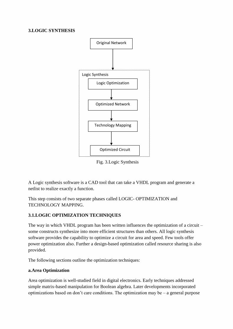
3.LOGIC SYNTHESIS
Fig. 3.Logic Synthesis
A Logic synthesis software is a CAD tool that can take a VHDL program and generate a
netlist to realize exactly a function.
This step consists of two separate phases called LOGIC- OPTIMIZATION and
TECHNOLOGY MAPPING.
3.1.LOGIC OPTIMIZATION TECHNIQUES
The way in which VHDL program has been written influences the optimization of a circuit –
some constructs synthesize into more efficient structures than others. All logic synthesis
software provides the capability to optimize a circuit for area and speed. Few tools offer
power optimization also. Further a design-based optimization called resource sharing is also
provided.
The following sections outline the optimization techniques:
a.Area Optimization
Area optimization is well-studied field in digital electronics. Early techniques addressed
simple matrix-based manipulation for Boolean algebra. Later developments incorporated
optimizations based on don’t care conditions. The optimization may be – a general purpose
Original Network
Logic Synthesis
Logic Optimization
Optimized Network
Technology Mapping
Optimized Circuit
one or targeted at particular structures (e.g. programmable logic arrays). Also underlying
technology strongly affects the optimization.
Where area optimization is more difficult is when particular device technology is used. For
example, the Xilinx FPGA operates a number of CLBs. Each CLB can compute up to five
input Boolean expressions. If the expression involves six inputs then a second CLB is needed.
If four inputs are needed then chip area is wasted.
b.Speed optimization
Some measure of speed optimization is usually achieved by area optimization, as the area
optimization removes redundant circuitry and can shorten the critical path of the circuit.
However, further speed optimization can be performed.
A common approach is to identify the critical path and to work on reducing that. A simple
optimization might be to replace each component on the critical path with a higher rated (i.e.
faster but more power- intensive equivalent) but functionally equivalent component from the
library. Other optimization techniques might be to strip out strings of inverters from a design
or where, for example, AND gates are slower than OR gates to attempt to replace all ANDs
with ORs.
3.2.TECHNOLOGY MAPPING
After logic optimization has produced the optimized network, technology mapping
transforms this network into the final circuit. This is done by selecting pieces of the network
that can be implemented by one of the available circuit elements, and specifying how these
are to be interconnected. The circuit is optimized to reduce a cost function that typically
incorporates measures of both area and delay. Conventional approaches to technology
mapping have focused on using circuit elements from a limited set of simple gates, such as a
Standard Cell library. The complex logic blocks used in FPGAs presents difficulties for
library-based approaches because they can each implement a large number of functions.
a.PLACEMENT
The next step after technology mapping is placement of logic blocks. A number of efficient
techniques have been developed, which can be easily adapted to use for FPGAs.
b.ROUTING
Routing refers to the process of interconnecting the various logic blocks of the FPGA. Some
of the terms used in routing are:
Pin – a logic block input or output.
Connection – a pair of logic block pins that are electrically connected.
Net – a set of logic block pins that are to be electrically connected. A
net can be divided into one or more connections.
Wire segment – a straight segment of wire that is used to form a part of a connection.
Routing switch – a programmable switch that is used to electrically
connect two wire segments.
Track – a straight section of wire that spans the entire width or of a routing channel. A
track can be composed of a number of wire segments of various lengths.
Routing channel – the rectangular area that lies between two rows or two columns of logic
blocks. A routing channel contains a number of tracks.
Because of the complexity involved, the solution of large routing problems as those
encountered in FPGAs, usually requires a ”divide and conquer” strategy. This approach
involves three steps.
1)Partition the routing resources into routing areas that are appropriate for both the device to
be routed and the routing algorithm to be employed.
2)Use a global router to assign each net to a subnet of the routing areas. The global router
does not choose specific wire segments and routing switches for each connection, but rather it
creates a new set of routing problems.
3)Use a detailed router to select specific wire segments and routing for each connection,
within the restrictions set by the global router.
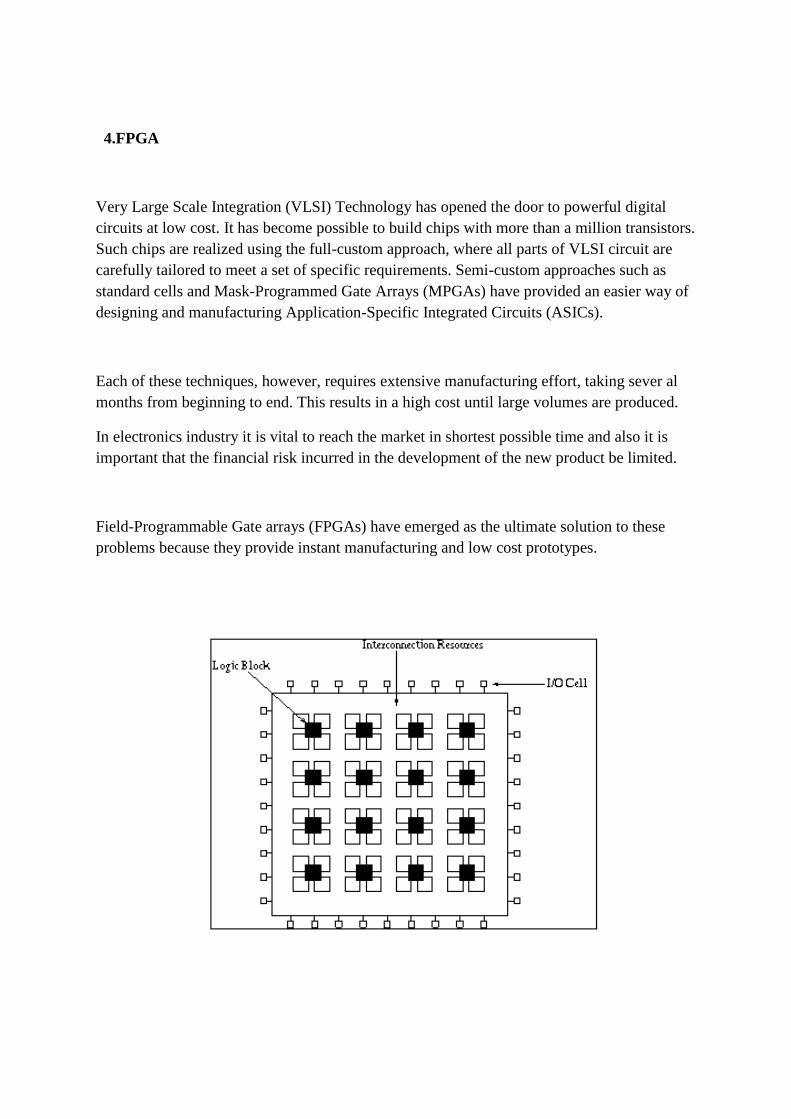
4.FPGA
Very Large Scale Integration (VLSI) Technology has opened the door to powerful digital
circuits at low cost. It has become possible to build chips with more than a million transistors.
Such chips are realized using the full-custom approach, where all parts of VLSI circuit are
carefully tailored to meet a set of specific requirements. Semi-custom approaches such as
standard cells and Mask-Programmed Gate Arrays (MPGAs) have provided an easier way of
designing and manufacturing Application-Specific Integrated Circuits (ASICs).
Each of these techniques, however, requires extensive manufacturing effort, taking sever al
months from beginning to end. This results in a high cost until large volumes are produced.
In electronics industry it is vital to reach the market in shortest possible time and also it is
important that the financial risk incurred in the development of the new product be limited.
Field-Programmable Gate arrays (FPGAs) have emerged as the ultimate solution to these
problems because they provide instant manufacturing and low cost prototypes.
ALU
Before writing the code of an 16 bit ALU first we have to understand what is ALU?.
ALU( Arithmetic and Logic unit) is a digital circuit that performs logical and arithmetic
operations.ALU is found inside every microprocessor or microcontroller in order to perform
logical and arithmetic operations. Logical operation involves all logical functions like
ANDing two or more inputs, OR,NOT,NOR etc.
Arithmetic operation involves function like addition, subtraction etc,
In the given code below the components of ALU are coded individually using VHDL and
then combined together in the main ALU code using port map technique.
Components of 8 bit ALU-
1) 8-bit adder-substractor- It performs addition and substraction for 8 bit input. A
carry line which acts as a signal acts as the deciding bit about what function the
circuit will perform. When the input carry signal is “0” the circuit acts as a 8 bit adder
and if the input signal is “1” the circuit acts as an adder.
2) 8-bit multiplier- This circuit is used to multiply 2 8 bit numbers and yield the
output as a 16 bit number.
3) 8-bit ALU- In the final circuit of ALU the components are combined together in a
single entity using port map.
Code for 8 bit adder-substractor
library ieee;
use ieee.std_logic_1164.all;
entity FULLADDER is
port (a, b, c: in std_logic;
sum, carry: out std_logic);
end FULLADDER;
architecture fulladder_behav of FULLADDER is
begin
sum <= (a xor b) xor c ;
carry <= (a and b) or (c and (a xor b));
end fulladder_behav;
--end of full adder
--definition of 4-bit addersub
library ieee;
use ieee.std_logic_1164.all;
entity FOURBITADD is
port (a,b: in std_logic_vector(3 downto 0);
Cin,m : in std_logic;
sum4bit: out std_logic_vector (3 downto 0);
Cout: out std_logic);
end FOURBITADD;
architecture fouradder_structure of FOURBITADD is
signal C,temp_carry: std_logic_vector (4 downto 0);
component FULLADDER
port(a, b, c: in std_logic;
sum, carry: out std_logic);
end component;
begin
process(b,m)
begin
for i in 0 to 3 loop
temp_carry(i)<=(b(i) xor m);
end loop;
end process;
FA0: FULLADDER
port map (a(0), temp_carry(0), Cin, sum4bit(0), c(1));
FA1: FULLADDER
port map (a(1), temp_carry(1), C(1), sum4bit(1), c(2));
FA2: FULLADDER
port map (a(2), temp_carry(2), C(2), sum4bit(2), c(3));
FA3: FULLADDER
port map (a(3), temp_carry(3), C(3), sum4bit(3), c(4));
Cout <= c(4);
end fouradder_structure;
--end of 4-bit addersub
--definition of 8-bitaddersub
library ieee;
use ieee.std_logic_1164.all;
entity EIGHTBITADD is
port ( a,b : in std_logic_vector(7 downto 0);
cin ,n: in std_logic;
sum8bit : out std_logic_vector(7 downto 0);
cout : out std_logic);
end EIGHTBITADD;
architecture eightadder_structure of EIGHTBITADD is
signal a1,a2,b1,b2,sum1,sum2 : std_logic_vector ( 3 downto 0);
signal cin_temp : std_logic;
component FOURBITADD
port (a,b: in std_logic_vector(3 downto 0);
Cin,m : in std_logic;
sum4bit: out std_logic_vector (3 downto 0);
Cout: out std_logic);
end component;
begin
process(a,b)
begin
for i in 0 to 3 loop
a1(i) <= a(i);
a2(i) <= a(i+4);
b1(i) <= b(i);
b2(i) <=b(i+4);
end loop;
end process;
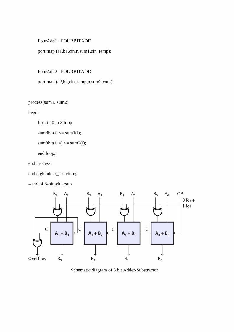
FourAdd1 : FOURBITADD
port map (a1,b1,cin,n,sum1,cin_temp);
FourAdd2 : FOURBITADD
port map (a2,b2,cin_temp,n,sum2,cout);
process(sum1, sum2)
begin
for i in 0 to 3 loop
sum8bit(i) <= sum1(i);
sum8bit(i+4) <= sum2(i);
end loop;
end process;
end eightadder_structure;
--end of 8-bit addersub
Schematic diagram of 8 bit Adder-Substractor
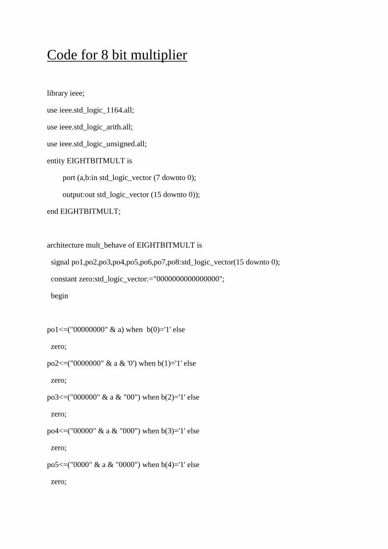
Code for 8 bit multiplier
library ieee;
use ieee.std_logic_1164.all;
use ieee.std_logic_arith.all;
use ieee.std_logic_unsigned.all;
entity EIGHTBITMULT is
port (a,b:in std_logic_vector (7 downto 0);
output:out std_logic_vector (15 downto 0));
end EIGHTBITMULT;
architecture mult_behave of EIGHTBITMULT is
signal po1,po2,po3,po4,po5,po6,po7,po8:std_logic_vector(15 downto 0);
constant zero:std_logic_vector:="0000000000000000";
begin
po1<=("00000000" & a) when b(0)='1' else
zero;
po2<=("0000000" & a & '0') when b(1)='1' else
zero;
po3<=("000000" & a & "00") when b(2)='1' else
zero;
po4<=("00000" & a & "000") when b(3)='1' else
zero;
po5<=("0000" & a & "0000") when b(4)='1' else
zero;
po6<=("000" & a & "00000") when b(5)='1' else
zero;
po7<=("00" & a & "000000") when b(6)='1' else
zero;
po8<=('0' & a & "0000000") when b(7) ='1' else
zero;
output<=(po8+ po7) + (po6 + po5) + (po4+po3) + (po2+po1);
end mult_behave;
--end of 8 bit multiplier
Final Code for 8 bit ALU
--definition of 8-bit ALU
library ieee;
use ieee.std_logic_1164.all;
use ieee.std_logic_arith.all;
use ieee.std_logic_unsigned.all;
entity ALU is
port(a,b: in std_logic_vector(7 downto 0);sel:in integer range 0 to 2;
final_output2:out std_logic_vector(15 downto 0);
final_output1:out std_logic_vector(7 downto 0));
end ALU;
architecture alu_structure of ALU is
signal output_adder,output_sub:std_logic_vector(7 downto 0);
signal output_mult: std_logic_vector(15 downto 0);
signal COUT,CIN:std_logic;
component EIGHTBITADD
port(a,b: in std_logic_vector(7 downto 0);
cin,n:in std_logic;
sum8bit: out std_logic_vector(7 downto 0);
cout:out std_logic);
end component;
component EIGHTBITMULT
port (a,b:in std_logic_vector (7 downto 0);
output:out std_logic_vector (15 downto 0));
end component;
begin
alu1: EIGHTBITADD
port map(a,b,CIN,'0',output_adder,COUT);
alu2: EIGHTBITADD
port map(a,b,CIN,'1',output_sub,COUT);
alu3:EIGHTBITMULT
port map(a,b,output_mult);
process(sel)
begin
if(sel=0) then
final_output1<=output_adder;
elsif(sel=1) then
final_output1<=output_sub;
else
final_output2<=output_mult;
end if;
end process;
end alu_structure;
--end of 8-bit ALU
9. FUTURE PROSPECTS
Results VHDL, One of the biggest job providing sector today, have a very bright future in the
coming time,but as the time is passing some other languages are making control over
designing, as for example Verilog HDL. Verilog HDL is a little bit better in processing speed
than VHDL. But on the other hand VHDL is also better in some fields like, all the three styles
of modeling(Data flow, Behavioral, Structural) in VHDL can be mixed together in the same
program i.e. VHDL is more user friendly than Verilog HDL.
But today all over world mainly VHDL is used for chip designing at low level. Till now there
are number of drawbacks in VHDL. As main drawback of VHDL is that, there are a number
of features in VHDL, that can be simulated but not synthesized. As, final shape to VHDL was
given by IEEE, hence IEEE is working on it continuously and trying to make available
simulation features to synthesis also.
So if talk about future prospectus of VHDL, it depends on success of IEEE. If IEEE got able
to implement such features that there remain no differences between simulation & synthesis
with higher processing speed and designing up to more lower level of abstraction, on that day
VHDL may take hold over all other HDL,s.