university of california, san diego in...
TRANSCRIPT

UNIVERSITY OF CALIFORNIA, SAN DIEGO
Anisotropic Artificial Impedance Surfaces
A dissertation submitted in partial satisfaction of the requirements for the degree
Doctor of Philosophy
in
Electrical Engineering (Electronic Circuits and Systems)
by
Ryan Gordon Quarfoth
Committee in charge:
Professor Daniel F. Sievenpiper, Chair
Professor Eric E. Fullerton
Professor Vitaliy Lomakin
Professor Siavouche Nemat-Nasser
Professor Gabriel M. Rebeiz
2014

Copyright
Ryan Gordon Quarfoth, 2014
All rights reserved.

iii
The Dissertation of Ryan Gordon Quarfoth is approved, and
it is acceptable in quality and form for publication on
microfilm and electronically:
____________________________________________
____________________________________________
____________________________________________
____________________________________________
____________________________________________
Chair
University of California, San Diego
2014

iv
DEDICATION
To my parents Carin and Gary.

v
TABLE OF CONTENTS
Signature Page ................................................................................................................ iii
Dedication ........................................................................................................................ iv
Table of Contents .............................................................................................................. v
List of Abbreviations ...................................................................................................... viii
List of Figures .................................................................................................................. ix
Acknowledgments .......................................................................................................... xiii
Vita .................................................................................................................................. xv
Abstract of the Dissertation ........................................................................................... xvii
Chapter 1 Introduction ................................................................................................... 1
1.1 Surface Waves ....................................................................................................... 1
1.2 Impedance Surfaces ............................................................................................... 3
1.3 Applications ........................................................................................................... 5
1.4 Scope of thesis ....................................................................................................... 6
Chapter 2 Surface Waves on Anisotropic Impedance Surfaces .................................... 7
2.1 Overview ............................................................................................................... 7
2.2 Artificial Tensor Impedance Surfaces ................................................................... 9
2.3 Periodic Unit Cells and Dispersion ..................................................................... 13
2.4 Eigenmode Simulation Method ........................................................................... 14
2.5 Rectangular and Diamond Unit Cell Results ...................................................... 16
2.5.1 Rectangular Cell ........................................................................................ 16
2.5.2 Diamond Cell ............................................................................................ 18
2.5.3 Variation of Lattice Length in Propagation Direction .............................. 20
2.6 Conclusion ........................................................................................................... 21
Chapter 3 Broadband Unit Cell for Highly-Anisotropic Impedance Surfaces ............ 22
3.1 Overview ............................................................................................................. 22
3.2 Anisotropic Unit Cell Theory .............................................................................. 22

vi
3.2.1 Tensor Impedance Surfaces ...................................................................... 22
3.2.2 Ideal Unit Cell Dispersion ......................................................................... 23
3.2.3 Higher Order Surface Modes ..................................................................... 25
3.3 Unit Cell Designs ................................................................................................ 27
3.4 Performance Figure of Merit ............................................................................... 33
3.5 Variation of Substrate Height and Permittivity ................................................... 36
3.6 Experiment .......................................................................................................... 39
3.7 Conclusion ........................................................................................................... 43
Chapter 4 Tensor Impedance Surface Waveguides ..................................................... 44
4.1 Overview ............................................................................................................. 44
4.2 Ideal Artificial Tensor Impedance Surface Waveguides ..................................... 45
4.2.1 Surface Waveguide Theory ....................................................................... 45
4.2.2 Tensor Impedance Simulation ................................................................... 48
4.2.3 Anisotropic Waveguide Results ................................................................ 53
4.2.4 Applications .............................................................................................. 58
4.2.5 Conclusion ................................................................................................. 65
4.3 Realized Artificial Tensor Impedance Waveguides ............................................ 65
4.3.1 Theoretical Dispersion of Realized Waveguide ........................................ 66
4.3.2 Unit Cell Analysis ..................................................................................... 67
4.3.3 Waveguide Dispersion and Fields ............................................................. 71
4.3.4 Near Field Measurements ......................................................................... 77
4.3.5 Curved Waveguide .................................................................................... 79
4.3.6 Analysis of Bending Loss ......................................................................... 83
4.4 Conclusion ........................................................................................................... 89
Chapter 5 Surface Wave Beam Splitter ....................................................................... 90
5.1 Overview ............................................................................................................. 90
5.2 Surface Waves and Transformations ................................................................... 90
5.3 Ideal Tensor Impedance Surface Wave Cloak .................................................... 93
5.4 Realized Surface Wave Beam Splitter ................................................................ 97
5.3.1 Unit Cell Design ......................................................................................... 97

vii
5.3.2 Beam Shift Design and Measurement ..................................................... 100
5.3.3 Surface Scattering ................................................................................... 103
5.5 Conclusion ......................................................................................................... 105
Chapter 6 Manipulation of Scattering Pattern Using Impedance Surfaces ............... 106
6.1 Overview ........................................................................................................... 106
6.2 Scattering Design .............................................................................................. 108
6.3 Unit Cell Design and Simulation ....................................................................... 111
6.4 Scattering Measurement .................................................................................... 115
6.5 Conclusion ......................................................................................................... 120
Chapter 7 Conclusion ................................................................................................. 121
7.1 Summary of Work ............................................................................................. 121
7.2 Future Work ...................................................................................................... 122
Bibliography .................................................................................................................. 123

viii
LIST OF ABBREVIATIONS
FOM Figure of merit
HFSS High frequency simulation software
PEC Perfect electric conductor
PMC Perfect magnetic conductor
PML Perfectly matched layer
SMA Sub-miniature type-A
TE Transverse electric
TM Transverse magnetic
VNA Vector network analyzer
Z Impedance

ix
LIST OF FIGURES
Figure 1.1: Surface wave mode on the boundary between dielectrics. ........................ 2
Figure 1.2: Surface wave mode on grounded dielectric slab. ...................................... 2
Figure 1.3: Surface waves excited on substrate near a patch antenna. ........................ 3
Figure 1.4: Grounded dielectric slab modeled as an impedance surface. .................... 3
Figure 1.5: Objects scatter incident waves in many directions. ................................... 5
Figure 2.1: Effective scalar impedance vs. propagation direction. ............................ 11
Figure 2.2: The fraction of the mode that is TE, γ, vs. propagation direction. .......... 12
Figure 2.3: Index of refraction vs. propagation direction. ......................................... 13
Figure 2.4: Unit cell examples. .................................................................................. 14
Figure 2.5: Example of simulation setup for diamond unit cell. ................................ 16
Figure 2.6: Dispersion of rectangular unit cells. ........................................................ 17
Figure 2.7: Reactance vs. frequency for rectangular unit cells. ................................. 18
Figure 2.8: Frequency vs. wavenumber for diamond unit cells. ................................ 19
Figure 2.9: Reactance vs. frequency for diamond unit cells. ..................................... 20
Figure 2.10: Reactance vs. frequency for multiple rectangular unit cell sizes........... 21
Figure 3.1: Impedance dispersion for an ideal tensor impedance surface. ................ 24
Figure 3.2: Dispersion diagram for an ideal tensor impedance surface. .................... 25
Figure 3.3: Typical dispersion diagram. .................................................................... 26
Figure 3.4: Vector field components for TM and TE modes. .................................... 27
Figure 3.5: Anisotropic unit cells. .............................................................................. 28
Figure 3.6: Previously published anisotropic unit cells. ............................................ 28
Figure 3.7: Perspective drawing of anisotropic ring-mushroom unit cell. ................. 29
Figure 3.8: Dispersion diagrams. ............................................................................... 31
Figure 3.9: TM effective surface impedance. ............................................................ 32
Figure 3.10: Effective surface index for ring-mushroom unit cells. .......................... 34
Figure 3.11: Index ratio and integration area of ring-mushroom unit cell. ................ 35
Figure 3.12: Unit cell performance vs. permittivity. .................................................. 37
Figure 3.13: Unit cell performance vs. substrate height. ........................................... 38
Figure 3.14: Photographs of each unit cell. ................................................................ 40

x
Figure 3.15: Measured and simulated dispersion curves. .......................................... 42
Figure 4.1: Impedance surface waveguide design. .................................................... 45
Figure 4.2: Ray optics model for surface impedance waveguide. ............................. 46
Figure 4.3: Geometry for Fresnel reflection. ............................................................. 48
Figure 4.4: Checkerboard structure. ........................................................................... 49
Figure 4.5: Simulation structure in HFSS for checkerboard surface. ........................ 51
Figure 4.6: Impedance vs. frequency. ........................................................................ 52
Figure 4.7: Effective scalar impedance vs. propagation direction. ............................ 53
Figure 4.8: Simulation structure of the checkerboard guide. ..................................... 54
Figure 4.9: Magnitude of the electric field. ................................................................ 55
Figure 4.10: Frequency vs. wavenumber plot for a checkerboard guide. .................. 57
Figure 4.11: Anisotropic waveguide with wave propagating in the guide. ............... 59
Figure 4.12: Anisotropic waveguide at orthogonal incidence. .................................. 59
Figure 4.13: Impedance tensor values for constant phase velocity. ........................... 60
Figure 4.14: Dispersion plots for constant phase velocity. ........................................ 61
Figure 4.15: Impedance tensor values for vp = 0.8c and vg = 0.65c. ........................... 62
Figure 4.16: Dispersion plots for the tensors labeled in Figure 4.15. ........................ 62
Figure 4.17: Anisotropic waveguides with propagating waves in the guides. ........... 64
Figure 4.18: Model of transparent surface impedance waveguide............................. 66
Figure 4.19: Physical representation of surface wave waveguide. ............................ 66
Figure 4.20: Unit cell dimensions. ............................................................................. 68
Figure 4.21: Dispersion relation for anisotropic and isotropic unit cells. .................. 69
Figure 4.22: Surface impedance vs. frequency. ......................................................... 69
Figure 4.23: Isofrequency impedance contours. ........................................................ 70
Figure 4.24: Photograph of tensor impedance surface waveguide............................. 72
Figure 4.25: Measurement setup for waveguide. ....................................................... 72
Figure 4.26: Dispersion of guided modes in tensor impedance surface waveguide. . 75
Figure 4.27: Normalized electric field magnitude. .................................................... 76
Figure 4.28: Normalized electric field magnitude above waveguide. ....................... 77
Figure 4.29: Measured fields. ..................................................................................... 78
Figure 4.30: Curved waveguide diagrams. ................................................................ 80

xi
Figure 4.31: Measured fields of curved waveguide. .................................................. 82
Figure 4.32: Measured field of orthogonally incident mode. ..................................... 83
Figure 4.33: Setup for ray optics analysis of curved waveguide. .............................. 85
Figure 4.34: Power loss over 90 degree bend on fabricated structure. ...................... 87
Figure 4.35: Frequency of half-power loss vs. center radius of the waveguide. ........ 88
Figure 4.36: Half power frequency vs. index of guiding region. ............................... 89
Figure 5.1: Illustration of microwave cloak. .............................................................. 91
Figure 5.2: Material properties of microwave cloak. ................................................. 92
Figure 5.3: Cloaking simulation setup and results. .................................................... 94
Figure 5.4: Uncloaked simulation setup and results. ................................................. 96
Figure 5.5: Unit cell dimensions. ............................................................................... 98
Figure 5.6: Photograph of a unit cell patch with measurements. ............................... 98
Figure 5.7: Dispersion diagram for ring-mushroom unit cell. ................................... 99
Figure 5.8: Impedance vs. frequency for ring-mushroom unit cell. ......................... 100
Figure 5.9: Fabricated structure setup. ..................................................................... 100
Figure 5.10: Photograph of beam shifter setup. ....................................................... 101
Figure 5.11: Measured normalized near field for series incidence at 13.5 GHz. ..... 102
Figure 5.12: Beam shift angle results. ...................................................................... 103
Figure 5.13: Measured field results for beam splitting surface at 13.5 GHz. .......... 104
Figure 5.14: Measured field results for isotropic impedance surface at 13.5 GHz. . 105
Figure 6.1: Scattering manipulation. ........................................................................ 106
Figure 6.2: Mode polarizations of incident radiation and surface waves................. 108
Figure 6.3: Scattering from metal rectangle. ............................................................ 109
Figure 6.4: Top view of scattering setup. ................................................................. 109
Figure 6.5: Ideal setup to prevent scattered radiation back towards the source. ...... 110
Figure 6.6: Backward scattering of ideal setup. ....................................................... 111
Figure 6.7: Top View of unit cell geometries. ......................................................... 112
Figure 6.8: Reflection phase of unit cells. ................................................................ 113
Figure 6.9: Surface index of TM and TE surface waves on incident region. .......... 114
Figure 6.10: Unit cell dispersion of transmitted section. ......................................... 115
Figure 6.11: Fabricated patterned rectangular surface. ............................................ 116

xii
Figure 6.12: Measurement Setup. ............................................................................ 117
Figure 6.13: Measured scattering transmission vs. rotation angle of the surface. ... 118
Figure 6.14: Measured reduction in backwards scattering. ...................................... 120

xiii
ACKNOWLEDGMENTS
I would first like to thank my advisor, Prof. Daniel Sievenpiper, for his guidance
and insight throughout the entirety of my research. I feel lucky to have had the
opportunity to work in his group, and my progress is testament to his vision, knowledge,
patience, and support. I would like to thank my committee members, Prof. Eric
Fullerton, Prof. Vitaliy Lomakin, Prof. Sia Nemat-Nasser, and Prof. Gabriel Rebeiz, for
taking the time to be part of my committee and for their comments and suggestions. I
would like to thank my parents, family, and friends, and especially everyone in the
Applied Electromagnetics Group.
The material in this dissertation is based on the following papers which are either
published, or under final process for publication.
Chapter 2 is based on and mostly a reprint of the following papers: R. Quarfoth,
D. Sievenpiper, “Artificial Tensor Impedance Surface Waveguides”, IEEE Transactions
on Antennas and Propagation, vol. 61, no. 7, pp. 3597-3606 2013; R. Quarfoth, D.
Sievenpiper, “Simulation of Anisotropic Artificial Impedance Surface with Rectangular
and Diamond Lattices”, IEEE Antennas and Propagation Symposium Digest, Spokane,
WA, USA, pp. 1498-1501, July, 2011.
Chapter 3 is based on and mostly a reprint of the following paper: R. Quarfoth,
D. Sievenpiper, “Broadband Unit Cell Design for Highly-Anisotropic Impedance
Surfaces”, IEEE Transactions on Antennas and Propagation, vol. 62, no. 8, pp. 1-10.
Chapter 4 is based on and mostly a reprint of the following papers: R. Quarfoth,
D. Sievenpiper, “Non-scattering Waveguides Based on Tensor Impedance Surfaces”,
Submitted to IEEE Transactions on Antennas and Propagation; R. Quarfoth, D.
Sievenpiper, “Artificial Tensor Impedance Surface Waveguides”, IEEE Transactions on
Antennas and Propagation, vol. 61, no. 7, pp. 3597-3606 2013.
Chapter 5 is based on and mostly a reprint of the following papers: R. Quarfoth,
D. Sievenpiper, “Surface Wave Scattering Reduction Using Beam Shifters”, IEEE
Antennas and Wireless Propagation Letters, vol.13, pp. 963-966, 2014; R. Quarfoth, D.
Sievenpiper, “Anisotropic Surface Impedance Cloak”, IEEE Antennas and Propagation

xiv
Symposium Digest, Chicago, IL, USA, July 8-14, 2012.
The dissertation author was the primary author of the work in these chapters, and
the coauthor (Prof. Daniel Sievenpiper) has approved the use of the material for this
dissertation.

xv
VITA
EDUCATION
2009 Bachelor of Science, Harvey Mudd College, Claremont, USA
2009 – 2014 Research Assistant, University of California, San Diego, USA
2011 Master of Science in Electrical Engineering, University of
California, San Diego, USA
2014 Doctor of Philosophy in Electrical Engineering, University of
California, San Diego, USA
PUBLICATIONS
R. Quarfoth, D. Sievenpiper, “Non-scattering Waveguides Based on Tensor Impedance
Surfaces,” Submitted to IEEE Transactions on Antennas and Propagation.
R. Quarfoth, D. Sievenpiper, “Broadband Unit Cell Design for Highly-Anisotropic
Impedance Surfaces,” IEEE Transactions on Antennas and Propagation, vol. 62, no. 8,
pp. 1-10.
D. Gregoire, J. Colburn, A. Patel, R. Quarfoth, D. Sievenpiper, "An Electronically-
Steerable Artificial Impedance Surface Antenna", IEEE Antennas and Propagation
Symposium Digest, Memphis, TN, July 6-11, 2014.
R. Quarfoth, D. Sievenpiper, “Surface Wave Scattering Reduction Using Beam
Shifters,” IEEE Antennas and Wireless Propagation Letters, vol.13, pp. 963-966, 2014.
M. Huang, S. Yang, F. Gao, R. Quarfoth, D. Sievenpiper, "A 2-D Multibeam Half
Maxwell Fish-Eye Lens Antenna Using High Impedance Surfaces," Antennas and
Wireless Propagation Letters, IEEE, vol.13, pp. 365-368, 2014.
R. Quarfoth, D. Sievenpiper, “Artificial Tensor Impedance Surface Waveguides.” IEEE
Transactions on Antennas and Propagation, vol. 61, no. 7, pp. 3597-3606 2013.
R. Quarfoth, D. Sievenpiper, “Anisotropic Surface Impedance Cloak”, IEEE Antennas
and Propagation Symposium Digest, Chicago, IL, USA, July 8-14, 2012.
D. Sievenpiper, D. Dawson, M. Jacob, T. Kanar, S. Kim, J. Long, R. Quarfoth,
"Experimental Validation of Performance Limits and Design Guidelines for Small
Antennas", IEEE Transactions on Antennas and Propagation, vol. 60, no. 1, pp. 8-19,

xvi
January 2012.
R. Quarfoth, D. Sievenpiper, “Simulation of Anisotropic Artificial Impedance Surface
with Rectangular and Diamond Lattices”, IEEE Antennas and Propagation Symposium
Digest, Spokane, WA, USA, pp. 1498-1501, July, 2011.
R. Quarfoth, D. Sievenpiper, “Impedance Surface Waveguide Theory and Simulation”,
IEEE Antennas and Propagation Symposium Digest, Spokane, WA, USA, pp. 1159-
1162, July, 2011.
Md. Zakaria Quadir, Oday al-Buhamad, Kai D. Lau, Ryan Quarfoth, Lori Bassman,
Paul R. Munroe, Michael Ferry, “The effect of initial microstructure and processing
temperature on microstructure and texture in multilayered Al/Al(Sc) ARB sheets.”
Journal of Materials Research, 100 (2009), p. 1705.

xvii
ABSTRACT OF THE DISSERTATION
Anisotropic Artificial Impedance Surfaces
by
Ryan Gordon Quarfoth
Doctor of Philosophy in Electrical Engineering (Electronic Circuits and Systems)
University of California, San Diego, 2014
Professor Daniel F. Sievenpiper, Chair
Anisotropic artificial impedance surfaces are a group of planar materials that can
be modeled by the tensor impedance boundary condition. This boundary condition
relates the electric and magnetic field components on a surface using a 2x2 tensor. The
advantage of using the tensor impedance boundary condition, and by extension
anisotropic artificial impedance surfaces, is that the method allows large and complex
structures to be modeled quickly and accurately using a planar boundary condition.
This thesis presents the theory of anisotropic impedance surfaces and multiple
applications. Anisotropic impedance surfaces are a generalization of scalar impedance

xviii
surfaces. Unlike the scalar version, anisotropic impedance surfaces have material
properties that are dependent on the polarization and wave vector of electromagnetic
radiation that interacts with the surface. This allows anisotropic impedance surfaces to
be used for applications that scalar surfaces cannot achieve. Three of these applications
are presented in this thesis. The first is an anisotropic surface wave waveguide which
allows propagation in one direction, but passes radiation in the orthogonal direction
without reflection. The second application is a surface wave beam shifter which splits a
surface wave beam in two directions and reduces the scattering from an object placed on
the surface. The third application is a patterned surface which can alter the scattered
radiation pattern of a rectangular shape.
For each application, anisotropic impedance surfaces are constructed using
periodic unit cells. These unit cells are designed to give the desired surface impedance
characteristics by modifying a patterned metallic patch on a grounded dielectric
substrate. Multiple unit cell geometries are analyzed in order to find the setup with the
best performance in terms of impedance characteristics and frequency bandwidth.

1
Chapter 1 Introduction
Antennas have become a ubiquitous component of modern technology. Many
consumer electronic devices now include multiple antennas for communication at
different frequencies and for different protocols. Airplanes, ships, and various military
platforms use antennas for radar, imaging, communication, and multiple other
technologies. In all of these systems, antennas are often placed near other conductive
objects and electronics, and also near other antennas. In order for these systems to work
optimally, the currents generated on and near antennas must be controlled in order to
maintain antenna patterns, prevent damage to electronics, and scatter radiation in the
desired directions. These surface currents can be manipulated using impedance surfaces
that control the propagation of surface waves.
1.1 Surface Waves
Surface waves are an electromagnetic wave mode that propagate bound to a
surface. They can be excited by antennas or due to external radiation, and the field is
peak on the surface and decays exponentially away from the surface. Surface waves can
be excited on the planar region between two dielectrics as shown in Figure 1.1. Each
material extends infinitely in the y direction, and the surface wave can propagate in any
direction on the YZ plane. The fields decay exponentially away from the boundary in
both the positive and negative x direction. The decay has a different rate in each material
due to the different material properties.

2
Grounded dielectric structures also support surface waves as illustrated in Figure
1.2. A thin substrate with thickness much less than the wavelength is placed above a
ground plane. Above the substrate is vacuum. In this setup there is still exponential field
decay above the substrate. The field varies sinusoidally within the substrate and multiple
modes are supported depending on the order of this variation. The grounded dielectric
supports surface wave modes down to zero-frequency. This affects multiple microwave
structures including patch antennas, microstrip lines and printed circuits where surface
waves generally degrade performance.
An illustration of the degradation of the radiation pattern of a patch antenna is
shown in Figure 1.3. A patch antenna can be constructed by placing a square or
rectangular patch above a grounded dielectric slab. The main radiation lobe is normal to
the patch. However, the structure will also excite surface waves in the dielectric
substrate. These surface waves propagate away from the patch and can radiate at the
edge of the substrate or at other discontinuities. This radiation can interfere with and
degrade the desired radiation pattern of the patch. This interference can potentially be
mitigated by patterning the substrate using impedance surfaces to control the
Figure 1.1: Surface wave mode on the boundary between dielectrics.
Figure 1.2: Surface wave mode on grounded dielectric slab.

3
propagation of surface waves on the dielectric. Other antennas or components that are
integrated to dielectric substrates such as microstrip lines or printed antennas can also be
negatively affected by this phenomenon.
1.2 Impedance Surfaces
An impedance surface is an electromagnetic boundary condition that relates the
electric and magnetic fields on a surface. Impedance surfaces are useful because they
allow the simplification of nearly-planar structures whose thicknesses are small as
compared to the wavelength. In Figure 1.4 an illustration is shown of a grounded
dielectric slab which is modeled as an impedance surface.
The slab, which has thickness d, is modeled instead by a planar boundary
condition with a scalar impedance defined as ZS. Isotropic surfaces have scalar surface
impedance. The rate of field decay above the impedance boundary is the same as the
decay above the grounded dielectric slab. Similarly, the phase velocity and group
Figure 1.3: Surface waves excited on substrate near a patch antenna.
Figure 1.4: Grounded dielectric slab modeled as an impedance surface.

4
velocity of surface waves on the impedance boundary are the same as those propagating
within the dielectric slab. These similarities are what allow the grounded slab to be
modeled more simply as an impedance boundary. More complicated structures can also
be modeled in this manner and these are discussed further in Section 2.3 and Section
3.3. The advantage of this simplification is that it allows large structures to be
accurately-modeled efficiently.
The surface impedance relates the electric and magnetic fields that are tangential
to the surface. The surface impedance is a complex number whose real part represents
loss. Therefore, lossless surfaces are purely reactive. Isotropic surfaces have the same
surface properties for a wave traveling in any direction along the surface. Anisotropic
surfaces have direction-dependent properties, and their properties are discussed in-depth
in Section 2.2. The polarization of electric and magnetic fields is dependent on the type
of surface mode. Transverse magnetic (TM) and transverse electric (TE) modes are both
supported. The surface impedance of each of these modes is defined below.
transverse
gpropagatin
TMSH
EZ , , (1.1)
gpropagatin
transverse
TESH
EZ , . (1.2)
TM modes have electric field in the propagating direction and magnetic field in
the transverse direction. The reactance is positive for TM modes, and surfaces that
support TM modes are sometimes called inductive. Conversely, TE modes have
magnetic field in the propagating direction and electric field in the transverse direction.
TE modes have negative reactance, and surfaces that support TE modes can be called
capacitive. The TM mode is supported by grounded dielectric slabs (and other similar
structures) down to zero-frequency. This is the mode that is predominantly used in this
thesis. Depending on the structure of the material, multiple TM or TE modes can be
supported simultaneously or at different frequencies. Along with TM and TE modes,
anisotropic surfaces support hybrid modes which are a combination of both TM and TE.
These hybrid modes are discussed in Section 2.2.

5
1.3 Applications
There are multiple applications for impedance surfaces which control surface
wave propagation. As discussed in Section 1.1 and illustrated in Figure 1.3, impedance
surfaces can be used to minimize the negative effects of surface waves on antennas.
Impedance surfaces can also be used to alter the scattering characteristics of objects. An
illustration of this is shown in Figure 1.5. Objects can have complicated scattering
patterns of incident radiation due to their shapes. By patterning the exterior of the object
with impedance surfaces, the scattering characteristics can be altered to a more desired
pattern.
Surface waves can also be used to create antennas. Surface wave modes that are
leaky do not propagate losslessly and instead radiate power away from the surface.
Leaky wave antennas have been created by periodically modulating the surface
impedance. This creates an effect similar to a diffraction grating and these antennas are
also known as holographic antennas. In this thesis, multiple other applications will also
be discussed including waveguides, beam shifters and splitters, and plane wave
scattering. These applications, along with the rest of the thesis, are summarized in
Section 1.4.
Figure 1.5: Objects scatter incident waves in many directions.

6
1.4 Scope of thesis
The thesis presents on details from multiple projects, with the common theme of
anisotropic artificial impedance surfaces.
Chapter 2 covers background information on the fundamentals of anisotropic
impedance surfaces. The mathematical description of impedance surfaces is first
presented. This is followed by a discussion of periodic unit cells, which are used to
create impedance surfaces. A description of the simulation method used to analyze the
material properties of the unit cells is also presented.
Chapter 3 investigates of the properties of multiple unit cell geometries. The
ring-mushroom unit cell geometry is found to have best performance in terms of
bandwidth and impedance range. The effect of substrate height and permittivity on
performance is also discussed.
Chapter 4 presents anisotropic surface impedance waveguides. In the first
section, a theoretical analysis of the dispersion in these waveguides is discussed. A
transparent waveguide application is also proposed and simulated. In the second section
this transparent waveguide is fabricated in both straight and bent setups.
Chapter 5 studies a surface wave beam splitter. The device is created using two
adjacent beam splitters which are transformation electromagnetic devices. The structure
is fabricated and measured, and it is shown that it can reduce the scattering of surface
waves from an object placed on a surface.
Chapter 6 demonstrates a structure that can be used to alter the scattering of
plane waves from an object. An incident plane wave has a characteristic pattern of
scattering when incident on a rectangular object. This pattern is altered by patterning a
ground plane on top and bottom using anisotropic impedance surfaces. Measured results
show that the effect can be achieved over a large bandwidth.

7
Chapter 2 Surface Waves on Anisotropic
Impedance Surfaces
2.1 Overview
Artificial impedance surfaces are engineered, electrically-thin materials which
can support surface waves in bound or leaky modes. Isotropic impedance surfaces have
a scalar relation between the electric and magnetic fields tangent to the surface, and
have the same properties for surface waves traveling in any direction. Isotropic
impedance surfaces have been designed for various applications including a linear leaky
wave antenna [1], spiral leaky wave antenna [2], Luneburg lens antenna [3, 4], and
impedance surface waveguides [5]. Tensor impedance surfaces are a generalization of
isotropic impedance surfaces where the relation between electric and magnetic field is a
2×2 tensor. Guided surface waves on tensor impedance surfaces have been characterized
analytically [6]. A tensor impedance surface was used to make a circularly polarized
antenna from a linear feed [7], and a circularly polarized isoflux antenna [8]. Tensor
impedance surfaces were also used as a liner to create a hybrid-mode horn antenna [9,
10]. Metasurfaces have been used to create mantle cloaks by scattering cancellation [11-
13]. Tensor surface impedance waveguides [5, 14] and a surface wave cloak using beam
shifters [15] have also been studied on ideal boundary conditions.
In every experimental implementation mentioned above, a periodic unit cell was
used to achieve the desired surface impedance properties. The size and thickness of the
unit cell must be small as compared to the wavelength (generally around λ/10). Unlike
constitutive properties such as permittivity and permeability which are effects of the
atomic structure of a material, impedance surfaces and other metasurfaces derive
effective material properties from macroscopic periodic inclusions that are artificially
8
added to a material [16]. Impedance surfaces can be created in many ways such as
grounded dielectric slabs (e.g. [17]), corrugated surfaces [18, 19], pin-bed structures [20,
21], bump lattices [22], and variable dielectric height [23-25]. Currently the most
common method to create impedance surfaces at microwave frequencies is with printed
circuit boards. Printed circuit boards are popular because they have an established
industry that provides quick manufacturing and low prices as compared to custom made
materials. Printed circuit fabrication can include dielectric with planar metallic
inclusions created by etching, and drilled, plated metal vias. Multi-layer structures can
also be fabricated and a wide variety of substrates can be used. In this study, for
simplicity, we limit the impedance surface design to a grounded dielectric with an
etched top layer and plated vias. The design of printed circuit materials is limited by the
manufacturing capabilities of the fabrication companies. These capabilities define
minimum spacing of metal patches, and the minimum diameter of vias. Each design
discussed in this paper can be manufactured using standard materials and processes.
Previous work has shown that a grounded dielectric slab with a printed
anisotropic metal pattern on the top layer can be accurately modeled as an anisotropic
impedance surface [7]. However, analysis has also shown that there are conditions
where a grounded dielectric substrate with an anisotropic capacitive impedance deviates
from the standard tensor impedance boundary condition [26, 27]. This analysis is only
for printed circuit tensor impedance surfaces with no vias. Multiple other variations of
printed circuit structures have also been studied. Un-patterned grounded dielectric slabs
support surface waves from DC up to high microwave frequencies. Mushroom unit cells
were shown to both suppress surface waves over a bandgap region and also reflect
incident plane waves in phase [28]. Tunable, varactor diode loaded structures [29, 30],
and reactively loaded vias [31] have also been studied. Lumped additions to the unit cell
have not been considered in this study, although these components could potentially
increase anisotropy or improve bandwidth and are a possible topic for future research.
This chapter presents the fundamental characteristics of impedance surfaces.
Section 2.2 covers the mathematical background of tensor impedance surfaces. Section
2.3 introduces periodic unit cells which are used to realize impedance surfaces. Section

9
2.4 explains the methods used to analyze the unit cells and determine their material
properties. Section 2.5 presents a simple study of the properties of rectangular and
diamond unit cells.
2.2 Artificial Tensor Impedance Surfaces
Isotropic impedance surfaces have a single scalar parameter, ZS, which relates
the electric and magnetic fields as described by (1.1) and (1.2). Anisotropic impedance
surfaces have direction-dependent impedance properties and must instead be modeled
by a 2×2 tensor. For a surface on the X-Y plane, the tensor impedance matrix can be
defined in general as
yyyx
xyxx
ZZ
ZZZ . (2.1)
In this study we assume lossless, reciprocal surfaces where all tensor values must be
pure imaginary and Zxy = Zyx [21]. The boundary condition for the fields on the surface
is defined as [1]:
JZHzZE .ˆ. . (2.2)
We can expand (2.2) to get a relation for the surface field components
x
y
yyxy
xyxx
y
x
H
H
ZZ
ZZ
E
E. (2.3)
Unlike scalar impedance surfaces which support pure TM waves, tensor surfaces
support hybrid waves that contain both TM and TE field components. The TM and TE
modes are transverse with respect to the direction of propagation. For a TM-like mode,
both eigenvalues of the impedance tensor are inductive, the electric and magnetic fields
can be split into their components as [7]
TETM EjEE 1 , (2.4)
TETM HjHH 1 . (2.5)
For the TM-like mode γ is the fraction of the TE field component in the wave and is less
than 0.5 (at γ=0.5 there would be equal TM and TE power in the mode). Substituting
(2.4) and (2.5) into (2.3) gives [7]

10
cossin1
sincos1
cossin1
sincos1
0
0
0
00
k
k
ZZ
ZZ
jk
j
jk
j
Zz
z
yyxy
xyxx
z
z
, (2.6)
where k0 is the wave number in the medium, αz is decay constant of the wave
attenuating above the surface, Z0 is the impedance of free space, and θ is the direction of
wave propagation with respect to the X-axis. Assuming the values of the impedance
tensor are known, we can solve (2.6) for αz/k0 and γ to get [7]
122
0
2/122
222
0
222
0
22
0
0
sin2sincos2
sin2sincos
sin2sincos4
xxxyyy
yyxyxx
xxxyyy
yyxxxyyyxxxy
z
ZZZZ
ZZZ
ZZZZ
ZZZZZZZZjk
, (2.7)
and
122
0
2/1222
0
2
0
22
22
0
4
0
2/1
0
22
0
2
44cos4sin42
222sin2cos2
yyxxxy
yyxxxyyyxxxyyyxxxy
yyxxxxyyxyyyxxxy
ZZZZ
ZZZZZZZZZZZ
ZZZZZZZjZZZZZ
. (2.8)
In each case, the negative sign corresponds to a TM-like mode and the positive sign to a
TE-like mode. The αz/k0 ratio gives a normalized, θ-dependent, effective scalar surface
impedance value for a tensor surface. For a TM-like mode the effective scalar surface
impedance can be written as
0
0k
jZZ z . (2.9)
From (2.9), we have obtained a scalar value from the impedance tensor that represents
the effective impedance of a wave propagating in the θ-direction. A wave on an
isotropic TM surface with this impedance will have the same phase velocity and field
decay above the surface as a wave on the tensor surface. A plot of the effective scalar
impedance Z(θ) is shown in Figure 2.1. The effective scalar impedance plot forms a
peanut shape except at the isotropic limit where it becomes circular. For a tensor with
Zxy=0, the maximum and minimum effective scalar impedance values are oriented along

11
the x- and y- axes (as displayed in Figure 2.1).
In general the magnitude and direction of the principal axes correspond to the
eigenvalues and eigenvectors of the impedance tensor. The eigenvectors are always
orthogonal and the peanut shape is symmetric across the two axes formed by the
eigenvectors. Figure 2.2 shows a plot of γ as a function of propagation direction. For a
lossless, reciprocal tensor surface, γ is purely real. Along the principal axes of the
impedance tensor γ=0, and γ is maximized 45° away from the principle axes. Impedance
tensors with larger amounts of anisotropy will have larger γ values. For an isotropic
surface, γ=0 at all rotation angles. In the limit as Zxx goes to j∞Ω and Zyy goes to zero,
γ=0.5 at all rotation angles
Figure 2.1: Effective scalar impedance vs. propagation direction. In this case the
impedance tensor has values Zxx=j400Ω, Zxy=0, Zyy=j200Ω.
j100
j200
j300
j400
30
210
60
240
90
270
120
300
150
330
180 0

12
The effective refractive index can also be expressed with respect to propagation
direction by relating it to the wave vector components or the surface impedance. The
wave vector components are related as follows
2
0
222 kkk zyx . (2.10)
For inductive surfaces, the index can be solved in two forms using equations (2.9) and
(2.10):
2
0
22
00
11Z
Z
kkn z
, (2.11)
where β is the propagating wavenumber: β2=kx
2+ky
2. The index is greater than one for
any inductive impedance. Figure 2.3 shows that the index is nearly elliptical for a tensor
with principal indices of nx=1.46 and ny=1.03 (values that are realistically achievable).
For a tensor with Zxy=0 (as shown in Figure 2.1 and Fig. Figure 2.3), the simplified
elliptical index is defined as:
2
2
2
2 sincos
1
yx nn
n
, (2.12)
Figure 2.2: The fraction of the mode that is TE, γ, vs. propagation direction. For a
lossless, reciprocal tensor impedance γ is real. In both lines plotted Zxy=0 which
causes principal axes of the axes of the impedance tensor to be aligned with the X
and Y axes, and γ=0 at θ=0° and θ=90°.
0 20 40 60 800
0.1
0.2
0.3
0.4
0.5
(degrees)
Zxx=j133 Zyy=j399
Zxx=j133 Zyy=j1330
13
where nx and ny are calculated from (2.11) by replacing Z(θ) with Zxx and Zyy
respectively. We defined this approximate elliptical index such that the index value
matches (2.11) exactly along the principal directions of the tensor but assumes elliptical
variation at intermediate angles. For larger surface indices, n>5, the effective surface
index can deviate 5% or more from the elliptical shape and become peanut-like.
However, this corresponds to an impedance Z>1,845Ω, which is quite large and hard to
achieve with simple printed circuit structures.
2.3 Periodic Unit Cells and Dispersion
Impedance surfaces can be created by patterning periodic inclusions into a
material [16]. Planar artificial materials can be called metasurfaces more generally.
Printed circuit structures are commonly used because of the ease of fabrication of these
materials. Previous studies have investigated the patterning of metal patches on a
grounded dielectric substrate [7]. Isotropic impedance surfaces have been created using
Figure 2.3: Index of refraction vs. propagation direction. In this case the
corresponding impedance tensor has values Zxx=j400Ω, Zxy=0, Zyy=j100Ω. The
principal index values are nx=1.46 and ny=1.03 at 0° and 90° respectively. An
ellipse with these same principal values is also plotted.
0.5
1
1.5
30
210
60
240
90
270
120
300
150
330
180 0
Exact Index
Ellipse

14
square or hexagonal metal patches [28]. Creating anisotropic impedance surfaces
requires some anisotropy of the unit cell shape. Examples of unit cells for anisotropic
impedance surfaces are shown in Figure 2.4.
The anisotropic impedance can be represented as a 2×2 impedance tensor that
has three independent terms (off-diagonal terms are equal) as shown in (2.3). Ideally a
unit cell geometry can be constructed where each of the three independent terms in the
tensor correspond to a specific geometrical parameter of the cell. The eigenvalues of this
tensor give the maximum and minimum impedance values, and the eigenvectors give
the direction of these values. To ensure that eigenvector directions match the lattice
direction, unit cells must be chosen with two orthogonal mirror symmetry planes as
shown in Figure 2.4. Because of a lack of symmetry, a square lattice geometry with a
slit will not have equivalence between the slit angle and the major axis of the impedance
tensor. When using symmetric cell types, the three independent impedance variables
could be the cell length in each orthogonal direction and the cell rotation. Preferably the
impedance along either of the orthogonal directions is only a function of the cell
geometry in that direction. Properties of rectangular and diamond unit cells are analyzed
in Section 2.4. Further analysis of unit cell geometries is performed in 0.
2.4 Eigenmode Simulation Method
Ansys HFSS is a commercial full-wave electromagnetic solver that was used for
all simulations in this thesis. HFSS has multiple solvers which can be used for different
Figure 2.4: Unit cell examples. A square unit cell with a slit is shown on the left.
Three different unit cells with two symmetry planes are shown on the right.

15
problems. Using the eigenmode solver, a single unit cell can be drawn and a solution is
found for a mode propagating on an infinite lattice of this unit cell. In this section, the
HFSS simulation setup is discussed. The properties of rectangular and diamond unit
cells are simulated, and the results are presented in Section 2.5.
A series of aspect ratios for rectangular and diamond cell geometries were
simulated using Ansoft HFSS software. In each case the dielectric simulated was Rogers
RT/duroid 5880 (εr=2.2) with a thickness of 1.575mm. A vacuum of height 15mm was
placed above the dielectric. In other studies, the vacuum height was chosen to be taller
so that results at lower frequencies were more accurate. A metal patch was simulated
using a perfect electric boundary condition, and a perfect electric boundary was also
used on the top and bottom of the structure. The perfect electric boundary on the top was
found to give equivalent results to the perfectly matched layer (PML) boundary. The
PML boundary was not used because of longer solution times and less stable results. He
PEC boundary is valid at the top of the structure as long as the surface mode has
decayed sufficiently. A radiation boundary cannot be used with the eigenmode
simulator. A gap of 0.4mm was implemented between the patch and the edge of the unit
cell. An infinite lattice was solved using master-slave boundaries in the built-in
eigenmode solver in HFSS.
Figure 2.5 shows a simulation structure for a diamond unit cell shape. By
applying master-slave boundaries to the sets of parallel walls, an effective phase delay
exists across the structure. Based on the distance between the walls, this phase delay
corresponds to a wavelength. For rectangular structures, the delay is set only on one set
of walls and the perpendicular walls have a delay of zero. For the diamond structure,
both sets of parallel walls are assigned an equal (or opposite) delay. This defines a wave
traveling in a tip to tip direction along the diamond. In the diamond case, the
wavenumber is obtained based on the delay, the propagating length, and the angle of the
diamond at the tip. The eigenmode solution gives the mode frequencies that satisfy the
boundary conditions. We chose to solve for the first five modes of the structures. The
results can be plotted as a dispersion curve as the delay value is swept.

16
2.5 Rectangular and Diamond Unit Cell Results
2.5.1 Rectangular Cell
A series of rectangular unit cell geometries were tested. In each case, the length
of the structure in the propagating direction was 6mm. The transverse length was varied
to determine whether the non-propagating lattice dimension affects propagation. Figure
2.6 shows that the transverse length has a negligible effect on the dispersion
characteristics of the structure. Each of the six cell sizes plotted has nearly identical
values.
Figure 2.5: Example of simulation setup for diamond unit cell.
Long DimensionShort
Dim.
Metal
Patch
Gap between
edge of patch
and unit cell
wall
Vacuum
Dielectric
εr=2.2
Perfect electric
boundary on top

17
For TM surface waves, the impedance can be obtained from the dispersion
relation as follows:
2
0
0 1
k
kZZ TM
TM. (2.13)
The reactance vs. frequency relation for each unit cell dimension is plotted in Figure 2.7.
Since the dispersion relation showed negligible variation of properties based on
transverse unit cell length, we get the expected result that the impedance characteristics
do not vary with transverse unit cell length. This is important for patterning where
setting the impedance independently in either direction significantly lowers the
difficulty of making complex patterns.
Figure 2.6: Dispersion of rectangular unit cells. Frequency vs. wavenumber for unit
cells of constant propagating length and varying transverse length.
0 100 200 300 400 500 6000
5
10
15
20
25
k (m-1)
Fre
quency (
GH
z)
Frequency vs Wavenumber Across 6mm Dimension
0 200 400 6000
5
10
15
20
25
k (m-1)
Fre
quency (
GH
z)
Frequency vs Wavenumber Across 6mm Dimension
6x3mm
6x6mm
6x8mm
6x10mm
6x12mm
6x16mm
f=c/
40240440614.9
15
15.1
k (m-1)
Fre
quency (
GH
z)
Frequency vs Wavenumber Across 6mm Dimension
6x3mm
6x6mm
6x8mm
6x10mm
6x12mm
6x16mm
f=c/

18
2.5.2 Diamond Cell
A series of diamond-shaped unit cells were simulated for a propagating length of
6mm. In this case, 6mm corresponds to the tip-to-tip length of the diamond cell. Since
the rectangular cells were defined by their side lengths, this convention implies that a
6x6mm diamond cell has the same area as a 3√2×3√2mm square cell. Figure 2.8 shows
the dispersion relation for each of the diamond cells along with the corresponding
rectangular cell. For low k values the cells have similar characteristics. For high k
values, the unit cells have diverging values.
Figure 2.7: Reactance vs. frequency for rectangular unit cells. The unit cells have
constant propagating length and varying transverse length.
0 5 10 15 20100
150
200
250
300
350
400
450
Frequency (GHz)
Z (
j )
Reactance vs Frequency Across 6mm Dimension
0 5 10 15 20100
150
200
250
300
350
400
450
Frequency (GHz)
Z (
j )
Reactance vs Frequency Across 6mm Dimension
6x3mm
6x6mm
6x8mm
6x10mm
6x12mm
6x16mm
14.9 15 15.1
300
305
Frequency (GHz)
Z (
j )
Reactance vs Frequency Across 6mm Dimension
6x3mm
6x6mm
6x8mm
6x10mm
6x12mm
6x16mm

19
Figure 2.9 shows the reactance vs. frequency relation of the diamond cells. For
the cells where the propagating dimension is longer than the transverse dimension we
have similar impedance ranges and shapes. For cells where the propagating dimension is
shorter than the transverse dimension, the impedance increases significantly at the
highest frequencies. We can see in the 12×6mm cell that the dispersion relation has a
negative slope for k from approximately 600 m-1
to 1050 m-1
. Theoretical regions with
negative slope are often difficult to access experimentally, so the structure may not be
useful in this range. In Figure 2.9 we can see that the impedance rapidly rises at the
onset of the negative slope. The start of this rapid impedance increase corresponds to a
value of approximately Z=400jΩ which is the same maximum value of the square or
long-dimension diamond lattices. Thus, both structures have roughly the same useful
impedance range, but the rectangular structure has the added advantage that impedance
is independent of the transverse cell length.
Figure 2.8: Frequency vs. wavenumber for diamond unit cells. The unit cells have
constant propagating length and varying inverse length.
0 200 400 600 800 10000
5
10
15
20
25
30
35
k (m-1)
Fre
quency (
GH
z)
Frequency vs Wavenumber Across 6mm Dimension
0 500 10000
5
10
15
20
25
30
35
k (m-1)
Fre
quency (
GH
z)
Frequency vs Wavenumber Across 6mm Dimension
6x1mm
6x2mm
6x3mm
6x6mm
6x9mm
6x12mm
32mm
Square
f=c/

20
2.5.3 Variation of Lattice Length in Propagation Direction
The propagating unit cell dimension was varied to determine the effect it has on
the impedance of the unit cell. The results of 14 rectangular unit cell simulations are
shown in Figure 2.10. In all of the labels, the first value is the propagating length in mm,
and the second value is the transverse length in mm. Multiple curves are not visible in
the plot because they are blocked by another simulation that has an equal unit cell length
in the direction of propagation. In every case, the impedance range is from 100jΩ to
400jΩ. The increase in unit cell length keeps a (somewhat) similar reactance vs.
frequency shape, but with a reduced frequency range. For a single frequency, the
increase in propagating length corresponds to an increase in reactance.
Figure 2.9: Reactance vs. frequency for diamond unit cells. The unit cells have
constant propagating length and varying transverse length.
0 5 10 15 20 25 30 350
200
400
600
800
1000
Frequency (GHz)
Z (
j )
Reactance vs Frequency Across 6mm Dimension
0 10 20 300
100
200
300
400
500
600
700
800
900
1000
Frequency (GHz)
Z (
j )
Reactance vs Frequency Across 6mm Dimension
6x1mm
6x2mm
6x3mm
6x6mm
6x9mm
6x12mm
32mm
Square

21
2.6 Conclusion
This chapter has presented the fundamental characteristics of anisotropic
impedance surfaces. This has included the mathematical formulation of impedance
surfaces, their physical realization using periodic structures, and the simulation method
for analyzing unit cells.
Chapter 2 is based on and mostly a reprint of the following papers: R. Quarfoth,
D. Sievenpiper, “Artificial Tensor Impedance Surface Waveguides”, IEEE Transactions
on Antennas and Propagation, vol. 61, no. 7, pp. 3597-3606 2013; R. Quarfoth, D.
Sievenpiper, “Simulation of Anisotropic Artificial Impedance Surface with Rectangular
and Diamond Lattices”, IEEE Antennas and Propagation Symposium Digest, Spokane,
WA, USA, pp. 1498-1501, July, 2011.
Figure 2.10: Reactance vs. frequency for multiple rectangular unit cell sizes. All
dimensions are in mm. The first value is the length of the propagating dimension,
and the second value is the length of the transverse dimension.
0 5 10 15 20 25 30 35100
150
200
250
300
350
400
450
500
Frequency (GHz)
Reacta
nce (
j )
Reactance vs Frequency for Rectangular Unit Cells
6x3 & 6x6 3x3
8x636x6

22
Chapter 3 Broadband Unit Cell for
Highly-Anisotropic Impedance Surfaces
3.1 Overview
Impedance surfaces are built from periodic unit cells as described in Section 2.3.
Isotropic impedance surfaces generally use square or hexagonal unit cells with patches
that have this same shape. In order to create an anisotropic impedance surface, the unit
cell must have some anisotropy. Unlike isotropic which only support pure TM and TE
modes, anisotropic surface support hybrid modes. It is found that when multiple modes
are supported at the same frequency these hybrid modes interfere with each other, and
the unit cell can no longer be used. In this chapter, multiple unit cell geometries are
analyzed to find which design has the best performance. The performance is quantified
using a figure of merit that accounts for both frequency bandwidth and the magnitude of
anisotropy.
3.2 Anisotropic Unit Cell Theory
3.2.1 Tensor Impedance Surfaces
The tensor impedance boundary condition specifies the field relation for a
lossless reciprocal impedance surface in the XY plane as described by (2.3). the
impedance tensor is a 2×2 matrix, and for a TM-like mode, all four values are purely
imaginary, the diagonal terms are inductive, and the off-diagonal terms are equal [7, 32].
Tensor impedance surfaces support hybrid modes that are mixtures of TM and TE
components. The fundamental mode on inductive surfaces is called “TM-Like” because
the TM component accounts for a majority of the wave power (an equivalent TE-like

23
mode also exists) [7]. The proportion of TM and TE components in a TM-Like mode is
dependent on the direction of propagation of the wave. In the principal directions of the
impedance tensor the TM-Like mode is purely TM and has no TE component. If the XY
coordinate system is aligned with these principal axes, the tensor will have no off-
diagonal terms in this coordinate system, and the impedance can be written without loss
of generality as follows:
yy
xx
Z
Z
0
0Z , (3.1)
where the impedance is explicitly defined to be frequency dependent. In this coordinate
system, a wave traveling in the x- or y-direction will have an effective impedance of Zxx
or Zyy respectively. Zxy is 0 since we have aligned the XY coordinate system with the
principal axis of the impedance tensor. At intermediate angles the impedance for TM-
like modes is defined by (3.2) and will be some value between Zxx and Zyy [7]:
0
0k
jZZ z , (3.2)
where αz is the exponential field decay of the mode above the surface as defined by
(2.7). A wave traveling on this anisotropic surface in the direction defined by θ will
have the same phase velocity and field decay as a wave on the scalar surface with an
impedance specified by (3.2). Real unit cells, along with being dispersive, deviate from
the theoretical impedance profile. In [26, 27], this discrepancy was characterized for
structures with no via. In this study we verify that bounded surface waves are supported
for any propagation direction, but accept that there will be some deviation from the ideal
theory.
3.2.2 Ideal Unit Cell Dispersion
Figure 3.1 shows an example of surface impedance dispersion where the x-
direction has high impedance and the y-direction has low impedance: Zxx(ω) > Zyy(ω).
Three intermediate angles are also plotted which represent surface waves traveling
between the x- and y-directions. At any given frequency, the effective surface
impedance varies gradually from Zxx to Zyy. Real impedance surfaces generally have

24
minimal anisotropy at low frequencies where impedance is also very small. As
frequency increases, the magnitude of the impedance and the level of anisotropy both
increase.
The wavenumber for a TM-like mode can be solved from the surface impedance
as follows [28]:
2
0
2
1Z
Z
ckTM
, (3.3)
where Z0 is the impedance of free space. An example of an expected dispersion plot for
a tensor impedance surface is shown in Figure 3.2. Under certain conditions, real unit
cells do not have the correct directionally dependent dispersion and cannot be used as
impedance surfaces.
Figure 3.1: Impedance dispersion for an ideal tensor impedance surface. Each curve
represents the expected impedance dispersion relation for propagation of a surface
wave mode in a different direction. The high and low impedance modes propagate in
orthogonal directions. At intermediate directions the impedance will gradually shift
from the low to the high impedance value.

25
3.2.3 Higher Order Surface Modes
Printed circuit impedance surfaces support multiple bound surface modes. For
isotropic impedance surfaces these modes are purely TM or TE, and a typical dispersion
diagram for the lowest two modes of an impedance surface using a grounded dielectric
substrate is shown in Figure 3.3. Figure 3.4 shows the field components of TM and TE
modes traveling in the x- and y-directions. The field polarizations can be rotated by 90
degrees from the x-direction to obtain the y-direction components. However, Figure 3.4
has instead been drawn to show the similarities between the x-direction TM mode and
the y-direction TE mode (and similarly the y- direction TM and x-direction TE modes).
The in-plane electric and magnetic field polarizations are identical, and the difference is
only in the out of plane component. Above the TE cutoff frequency both TM and TE
modes are supported. In this region, for anisotropic structures, the ideal spatial
dispersion (shown for the TM mode in Figure 3.2) does not occur. The ideal theory
stipulates that the mode is purely TM on the principal axis, becomes TM-like as the
direction of propagation is rotated away from the principal axis, and becomes purely
Figure 3.2: Dispersion diagram for an ideal tensor impedance surface. The relative
locations of the curves correspond to the positions shown in Figure 3.1. The light
line represents the dispersion relation of a plane wave in a vacuum. The low
impedance mode is closest to the light line and the high impedance mode is the
furthest from the light line. As the propagation direction is rotated from the low
impedance direction to the high impedance direction the dispersion relation will
gradually shift.

26
TM again at the orthogonal principal axis. In actuality, pure TM modes are supported
along each principal axis, but the rotation between these pure TM modes does not occur.
Instead, as the direction of propagation is gradually rotated from one principal axis to
the orthogonal axis, the original TM mode gradually shifts to become a TE mode. The
result of this phenomenon is that anisotropic unit cells cannot be used at frequencies
where both TE and TM modes are supported because the surface does not support the
desired TM-like mode in every direction. This will be shown explicitly in Section 3.3.
Figure 3.3: Typical dispersion diagram. The impedance surface is designed using a
grounded dielectric substrate. The light line is the dispersion relation of a plane wave
in a vacuum. The TM mode is the lowest order mode and remains below the light
line. The TE mode starts above the light line as a leaky mode (marked as a dashed
section) and becomes a bound surface wave above some cutoff frequency (marked as
a solid line).

27
3.3 Unit Cell Designs
The goal of the unit cell design is to create a structure that has a large frequency
bandwidth of highly anisotropic surface impedance. One stipulation for the design is
that the unit cell must support bound surface waves in any direction along the surface.
Corrugated surfaces and some printed circuit designs are highly anisotropic, but only
support surface waves along a specific direction.
Three unit cell designs were studied. Each design used a grounded 1.575mm
thick Rogers 5880 substrate (εr = 2.2), and the unit cell is square with lattice dimension a
= 4mm. Diagrams of the three unit cells are shown in Figure 3.5. Figure 3.5a shows a
patch design with no via. This design type, which includes a patch on a grounded
dielectric substrate, has been published in multiple previous studies. These previous
designs are illustrated in Figure 3.6, where Figure 3.6a shows a sliced patch structure
[7], Figure 3.6b shows a sliced circular patch design [8], and Figure 3.6c shows a
rectangular unit cell [33]. All three designs illustrated in Figure 3.6 have similar
impedance ranges and anisotropy levels as the anisotropic patch unit cell in Figure 3.5a.
Figure 3.4: Vector field components for TM and TE modes. The surface waves are
traveling in the x- and y-directions.
k E H k E H
k E H k E H

28
Figure 3.5b shows an anisotropic mushroom unit cell design. A traditional
mushroom unit cell contains a square patch over a square unit cell [28], and an
anisotropic mushroom cell has a rectangular patch. Figure 3.5c shows an anisotropic
ring-mushroom unit cell. Figure 3.7 shows a perspective view of this ring-mushroom
unit cell. The ring-mushroom structure has the same outer patch perimeter, but the
interior region is sliced so that the via only connects to a smaller patch on the top plane.
The total structure is a planar ring that surrounds a smaller mushroom. The result of the
Figure 3.5: Anisotropic unit cells. (a) shows an anisotropic patch structure, (b)
shows an anisotropic mushroom structure, and (c) shows an anisotropic ring-
mushroom structure. In each case a top view is shown of the unit cell where the outer
area is dielectric and the inner region is a metal patch on top of the dielectric. In (b)
and (c) the circular region represents a metal via. The via has a diameter of 0.3mm.
In each unit cell, the outer patch dimension is 2×3.75mm. In (c) the inner patch has
dimension 1.4×2.4mm and the gap between the inner and outer patch is 0.15mm on
all sides.
Figure 3.6: Previously published anisotropic unit cells. (a) shows a sliced patch
structure, (b) shows a sliced circular patch structure, and (c) shows a rectangular
patch and unit cell.

29
decreased inner patch size is a decrease in the inductance of the unit cell as compared to
the traditional mushroom structure. The inner patch size can be tuned so that at one
extreme, the structure is identical to a mushroom, and at the other extreme, the structure
is similar to a patch (with some deviation due to the via). The ring-mushroom structure
has additional capacitance within the unit cell in series with the capacitance between
unit cells. The additional series capacitance lowers the overall sheet capacitance of the
structure. However, simulations of via-less structures show that the dominant effect on
the dispersion relation is solely due to capacitance between unit cells which is identical
for patch, mushroom, and ring-mushroom structures.
Each unit cell was simulated using the eigenmode solver in Ansys HFSS version
15.0 (a full-wave, commercial software package). The unit cells were oriented so that
waves traveling at 0° are in the high impedance direction waves traveling at 90° are in
the low impedance direction (the x-axis is defined as 0°). Two intermediate angles were
also simulated, and these were for phase velocity at 30° and 60° from the x-axis. The
dispersion results of the patch unit cell are shown in Figure 3.8a. The TE cutoff for this
geometry is at 14 GHz and below the cutoff only TM modes are supported by the
structure. In this region below TE cutoff, the TM modes for all directions are nearly
identical. However, despite being nearly isotropic, the impedance range shifts gradually
from high to low as the wave propagation direction is rotated from 0° to 90°, as can be
Figure 3.7: Perspective drawing of anisotropic ring-mushroom unit cell. Figure 3.5c
is a top view of this structure. A ground plane is at the bottom of the unit cell and the
dielectric is shown by the rectangular prism outline. A cylindrical via extends from
the ground plane to the top of the dielectric. The patches are on the top surface of the
dielectric.

30
seen in Figure 3.9a. Above the TE cutoff, the TM mode dispersion does not have the
ideal form that is plotted in Figure 3.2. The TM dispersion curves for 0° and 90° are
separated as desired, but the dispersion for 30° and 60° do not lie between the principal
modes. Instead, the TM mode at 0° gradually shifts to become the TE mode at 90°.
Similarly the TM mode at 90° gradually shifts into the TE mode at 0°. As discussed in
Section 3.2, the TM and TE modes that travel in perpendicular directions have very
similar field components. The simulations show that in the region above TE cutoff
where both TM and TE modes are supported by the structure, the TM mode dispersion
does not follow the ideal case and cannot be modeled as a tensor impedance surface.
Therefore, the usable frequency range for this patch structure has very low and nearly
isotropic surface impedance as shown in Figure 3.9a.

31
Figure 3.8: Dispersion diagrams. The plots show results for (a) patch, (b)
mushroom, and (c) ring-mushroom unit cells. Four propagation directions are shown
where 90° and 0° are the principal axes of the impedance tensor. The dispersion of
light in a vacuum is shown as a black dashed line.
100 200 300 400 500 600 700
5
10
15
20
25
k (m-1)
Fre
quency (
GH
z)
(a)
90
60
30
0
Light
100 200 300 400 500 600 700
5
10
15
20
25
k (m-1)
Fre
quency (
GH
z)
(b)
90
60
30
0
Light
100 200 300 400 500 600 700
5
10
15
20
25
k (m-1)
Fre
quency (
GH
z)
(c)
90
60
30
0
Light

32
The patch unit cell is not usable as a tensor impedance surface above the TE
cutoff. A mushroom unit cell avoids this issue by pushing the entire TM mode below the
TE cutoff. Figure 3.8b shows the dispersion relation for an anisotropic mushroom
structure. The TM mode now has a maximum frequency below the TE cutoff and there
is a bandgap region between the TM and TE modes. Simulations of mushroom
structures predict backward waves where phase and group velocity have opposite signs.
However, to our knowledge, backward, bound, microwave-frequency, surface waves
have never been measured. Experimental implementations have used volumetric 3D
metamaterials [34, 35], transmission line modes [36-38], or leaky modes [39-41]. Along
with being difficult to measure, backward waves also occur at frequencies where two
Figure 3.9: TM effective surface impedance. The plots show results for (a) patch,
(b) mushroom, and (c) ring-mushroom unit cells. The cutoff frequency for the TE
mode is shown in (a) and (c). In (b) the cutoff frequency lies at 14GHz. The
impedance tensor has principal axes at 0° and 90°.
5 10 15 20 250
100
200
300
400
500
600
Z (
j )
Frequency (GHz)
(a)
90
60
30
0
TE Cut
4 6 8 10 120
500
1000
1500
Z (
j )
Frequency (GHz)
(b)
90
60
30
0
4 6 8 10 12 14 160
200
400
600
800
1000
Z (
j )
Frequency (GHz)
(c)
90
60
30
0
TE Cut

33
different TM modes are supported, and this could cause interference between the modes.
Therefore, backward wave regions are not considered usable for the unit cell, and as
seen in Figure 3.9b, the usable impedance range has a maximum value of Zxx = j500Ω
and Zyy = j170Ω. Above this range only backward waves are supported on the surface.
The mushroom cell successfully suppressed the TM mode below the TE cutoff
frequency, but it was suppressed so far that the backward wave region is dominant and
the unit cell is not highly anisotropic over a broad bandwidth. The ring-mushroom
structure suppresses the TM mode only enough to move it below the TE cutoff, but not
so much that the mode becomes a backward wave. Figure 3.8c and Figure 3.9c show the
dispersion and impedance relations of the ring-mushroom structure. The ring is tuned so
that the TM mode peaks at the TE cutoff. For a fixed outer ring dimension, the tuning
involved modifying the size of the inner patch. The ring-mushroom unit cell has a
maximum anisotropy of Zxx = j1000Ω and Zyy = j280Ω. This is a significantly more
anisotropic impedance than is obtainable with patch or mushroom structures.
In this paper the characteristics of the unit cell are determined by simulation as
described above, and by experiment in Section 3.6. Multiple types of analytical models
have also been created to study surface wave dispersion on similar structures. A
transverse resonance method was used on an anisotropic patch geometry [26, 27],
homogenization models were used with wire-medium slabs and mushroom structures
[42], and a pole-zero matching method has been applied to patches on a grounded
dielectric slab [43]. A potential topic for future study is to apply one of these methods,
or another method, to create an analytical model for the ring-mushroom structure.
3.4 Performance Figure of Merit
The performance of the unit cells are compared using a figure of merit (FOM)
that quantifies the anisotropy of the unit cell. The FOM is based on the effective surface
index (henceforth referred to simply as “index”). The index for TM-like modes on a
tensor impedance surface is direction dependent and can be related to the effective
surface impedance, (3.2), as follows:

34
2
0
1
Z
Zn
, (3.4)
As with volume media, the index defines the phase velocity of the wave where
vp=c/n. The index for the ring-mushroom structure is shown in Figure 3.10, and it
approaches one as surface impedance approaches zero. A FOM for anisotropy could use
either the ratio of impedances or indexes for the modes propagating along the principal
axes. However, the index ratio gives a more relevant measurement of anisotropy than
the impedance ratio because at low surface impedances, high impedance ratios do not
necessarily imply a highly anisotropic impedance surface. For example, a tensor surface
with Zxx = j20Ω and Zyy = j10Ω has an impedance ratio of 2, but the corresponding index
ratio is 1.001.
The FOM for highly anisotropic unit cells is designed to reward cells that have large
index ratios over a large relative bandwidth. The FOM is defined below:
frequency low
highdf
fn
fn
fFOM 1
1, (3.5)
where the range of the integral is the frequency range of the unit cell, f is frequency,
nhigh is the index of the high-impedance principal axis, and nlow is the index of the low-
impedance principal axis. The ratio of the indexes is one for an isotropic material, and
Figure 3.10: Effective surface index for ring-mushroom unit cells.
4 6 8 10 12 14 161
1.5
2
2.5
3
Frequency (GHz)
Index
90
60
30
0
Cutoff

35
this is subtracted off in the FOM so that the value only increases in anisotropic regions.
The index ratio and the relevant integrated area are shown in Figure 3.11. The integral is
scaled by inverse frequency so that the FOM is equal for equivalent relative frequency
bandwidths (for example the FOM would be the same between 1-2GHz and 10-20GHz
for appropriately frequency-scaled indexes).
The FOM integral is over the entire frequency range of the mode which starts at
DC and goes up to the maximum of the TM mode. The TM maximum is defined as
whichever is lowest between the TE cutoff, the onset of the backward wave region, or
the mode cutoff at a = λ/2. The integration method for determining the FOM is
advantageous because it does not rely on any arbitrary performance cutoff. If a more
traditional frequency bandwidth were used, some index ratio cutoff would need to be
created which defined the threshold for a “highly anisotropic” material. For instance, an
alternative bandwidth criterion could be the range of frequencies where the index ratio is
greater than 1.1 (or any other arbitrary cutoff). This criterion was analyzed and gave
qualitatively similar results to the FOM defined in (3.5). However, (3.5) is preferred
Figure 3.11: Index ratio and integration area of ring-mushroom unit cell. The index
ratio, shown as a dashed line, is the ratio of the 0 and 90 degree curves shown in
Figure 3.10 after subtraction by one. The integration area is the region which
contributes to the FoM. In the FoM integral, each point is also divided by the
frequency.
6 8 10 120
0.2
0.4
0.6
0.8
1
1.2In
dex R
atio
- 1
Frequency (GHz)
Index Ratio - 1
Integration Area

36
because it relies only on the fundamental characteristics of the unit cell and not a
subjectively applied cutoff.
The patch, mushroom, and ring-mushroom unit cells analyzed in Section 3.3
have FOM values of 0.015, 0.062, and 0.112 respectively. This shows that the ring-
mushroom structure significantly outperforms the patch and mushroom structures for
this substrate. In the following section, the substrate is changed and the effect on the
FOM is analyzed.
3.5 Variation of Substrate Height and Permittivity
Figure 3.8 and Figure 3.9 demonstrate the effects of altering the patch geometry
and via presence on dispersion characteristics. The substrate permittivity and height also
affect the properties of the unit cell. In Section 3.3 the substrate was Rogers 5880 (εr =
2.2) with a height of 1.575mm. In this section the substrate permittivity and height are
varied independently.
In Figure 3.12, the unit cell has a height of 1.575mm, and εr is swept from 2.2 to
10.2, which is the range for commonly available, low-loss dielectrics. The other
dimensions of the unit cell are held constant, along with the loss tangent. For the patch,
the FOM increases with εr. The increased εr makes the substrate electrically thicker and
pushes the TM mode to lower frequencies which have higher impedance. For the same
wavenumber, lowering the frequency of a TM mode increases the surface impedance.
This relation can be seen by rearranging (3.3):
2
0 1
ckZZ TM
TM. (3.6)
Note that ZTM is a positive imaginary number. Because of the significantly improved
performance, practical designs consisting of patch unit cells generally use large
dielectrics such as εr=10.2.

37
The mushroom structure has a slight decline in FOM with εr. As with the patch,
the increased εr causes the TM mode to lower in frequency. However, the mushroom,
unlike the patch, has a backward wave region. For increasing εr, the onset of this
backward wave region lowers in frequency further than the overall decrease of the
mode. The result is the gradual decrease in FOM since backward wave regions are not
included. The ring-mushroom structure increases in FOM initially but then falls and
plateaus. In this case, the dimensions of the ring-mushroom structure are specifically
tuned for εr=2.2. As the permittivity increases, the TE mode cutoff lowers and around εr
= 4 starts to interfere with the TM mode, just as in the patch structure. Since integration
region of the FOM stops at the onset of the TE mode, the result is the decrease in FOM
for large εr. If the structure were tuned specifically for each εr value, the FOM would
rise with permittivity.
In Figure 3.13a, the permittivity was fixed at εr=2.2 and the substrate height was
swept from 0.5mm to 3.25mm. The FOM increases with substrate height for each unit
cell design. For the patch, the increase in FOM is because the increased height, as with
increased permittivity, lowers the frequency of the TM mode and thus raises the
impedance as described by (3.6). The mushroom structure also shows FOM
improvement with increased substrate height. For the mushroom structure, increased
Figure 3.12: Unit cell performance vs. permittivity. The substrate permittivity is
swept from εr=2.2 to εr=10.
2 4 6 8 100
0.05
0.1
0.15
r
Bandw
idth
Fig
ure
of M
erit
Patch
Mushroom
Ring-Mushroom

38
substrate height, unlike increased substrate permittivity, lowers the overall TM mode
frequency more significantly than it lowers the onset frequency of backward waves. The
ring-mushroom structure has increased FOM, and in this case, the TM mode is lowered
more quickly than the TE mode so there is no plateau as seen in Figure 3.12. The ring-
mushroom structure performs the best at all heights except for very thin substrates
where the mushroom structure performs better.
In Figure 3.13b the substrate permittivity is set to εr=10.2, and the substrate
height is again swept from 0.5mm to 3.25mm. The patch unit cell now has a slightly
higher bandwidth than the mushroom structure, which is consistent with the εr=10.2
(a)
(b)
Figure 3.13: Unit cell performance vs. substrate height. The substrate height is
swept from 0.5mm to 3.25mm for (a) εr=2.2 and (b) εr=10.2.
0.5 1 1.5 2 2.5 30
0.05
0.1
0.15
0.2
0.25
Height (mm)
Bandw
idth
Fig
ure
of M
erit
Patch
Mushroom
Ring-Mushroom
0.5 1 1.5 2 2.5 30
0.05
0.1
0.15
0.2
0.25
Height (mm)
Bandw
idth
Fig
ure
of M
erit
Patch
Mushroom
Ring-Mushroom

39
region of Figure 3.12. All three unit cells again show bandwidth improvement as the
substrate height increases. The ring-mushroom structure again has a bend in the curve
which corresponds to the frequency at which the TM mode is suppressed completely
below the TE mode. The FOM for the ring-mushroom unit cell is still significantly
higher than either the patch or mushroom unit cells except for very thin substrates.
3.6 Experiment
Three surfaces were fabricated using printed circuit fabrication technology. The
surfaces were each 10×16 inches with the high impedance direction along the 10 inch
dimension. Photographs of zoomed-in sections of each surface are shown in Figure 3.14.
The unit cells were designed identically to those simulated in Section 3.3: εr = 2.2, a =
4mm, outer patch dimensions of 2×3.75mm, inner patch dimensions of 1.4×2.4mm and
gaps between the inner and outer patch of 0.15mm on all sides. The only difference
between the experimentally fabricated surfaces and the simulated versions is a
fabricated via diameter of 0.38mm instead of the desired 0.3mm simulated dimension
(due to a larger-than-anticipated drill used in fabrication). Each surface was measured
using a near field scanner. A surface wave was excited using a small triangular antenna,
and a vertically polarized probe was scanned 2mm above the surface along a line. An
Agilent E5071C vector network analyzer recorded the phase of the surface wave at
200μm increments. Magnetic radar absorbing material was placed at the edge of the
surfaces to limit reflections. The phase velocity of the surface wave was obtained from
the phase measurements, and this phase velocity was used to determine the dispersion
relation. Each surface was measured along both principal axes and also at an angle
bisecting the principal axes at 45°.

40
For the principal axes, the measured dispersion is compared directly to the
simulated versions comparable to those shown in Figure 3.8 (the High-Z and Low-Z
principal axes are 0° and 90° respectively). The simulated response is slightly different
than Figure 3.8 due to the increased via diameter. For non-principal axis measurements,
simulation and experiment cannot be compared directly. In simulation, the unit cells are
measured using the eigenmode simulator in which the phase across the unit cell is
defined. In this way, the curves labeled as 30° and 60° in Figure 3.8 are defined with
(a)
(b)
(c)
Figure 3.14: Photographs of each unit cell. The photographs show (a) patch unit
cell, (b) mushroom unit cell, and (c) ring-mushroom unit cell.

41
respect to the direction of the phase velocity. For the measured response, a straight line
in the physical space (not the phase space) was measured oriented 45° from the x-axis.
This 45° angle represents the angle of power flow over the unit cell and not the angle of
the phase velocity. For anisotropic materials, the direction of power flow is not the same
as the direction of phase velocity, and this has been studied specifically for surface
waves on structures with no via [44]. In order to relate phase velocity and power flow
(and compare the simulated and measured results) we have assumed elliptical phase
fronts on the surface. Real surfaces do not have perfectly elliptical phase fronts, but the
assumption is good enough to give closely matching measured results. At a given
frequency, the index in each principal direction is known, and each other direction is
obtained by the assumption of elliptical phase fronts. For a point on the ellipse, the
phase velocity is tangential to the ellipse, and the power flow is in the direction from the
center of the ellipse to the point. The phase velocity was swept in simulation to find the
modes where the angle of power flow was 45° as desired.
Measured and simulated dispersion curves are plotted in Figure 3.15. In Figure
3.15a, the dispersion of the patch structure is shown. As predicted by the simulated
results in Figure 3.8a, surface waves along the principal axes are supported up to at least
20 GHz (the upper frequency limit of the VNA). The high-Z measurement had a region
between 16.1 and 17.3 GHz where the measurement was extremely noisy and was
removed from the plot. Simulation predicts that the mode is supported here, but it is also
the frequency around which the TE mode crosses the TM mode. In the measurement,
this region is most likely noisy due to coupling between the TM and TE modes. At 45
degrees, the measurement no longer shows a surface wave above 15 GHz. For the patch
structure, simulation shows that the TE mode cutoff is at 13.8 GHz and the TE and TM
modes cross at 15 GHz. For the measurement, the TM mode is never supported above
15 GHz, and this is matched by the simulation which shows a breakdown of the TE
mode around this frequency.
42
(a)
(b)
(b)
Figure 3.15: Measured and simulated dispersion curves. Results are for (a) patch
unit cell, (b) mushroom unit cell, and (c) ring-mushroom unit cell. Measured curves
are solid lines, and simulated are dots. The simulated dispersion curves uses a via
diameter of 0.38mm to match the fabricated surfaces. The 0.3mm via diameter
simulations shown in Figure 3.8 have very similar dispersion, although not identical.
200 250 300 350 400 450 500 55010
12
14
16
18
20
k (m-1)
Fre
quency (
GH
z)
Low Z
45 Deg
High Z
Light
100 150 200 250 300 350 4006
7
8
9
10
11
12
Fre
quency (
GH
z)
k (m-1)
Low Z
45 Deg
High Z
Light
200 300 400 500 6009
10
11
12
13
14
15
k (m-1)
Fre
quency (
GH
z)
Low Z
45 Deg
High Z
Light

43
Figure 3.15b shows the dispersion for the mushroom structure. Measurement and
simulation show good agreement. The measurement curve tops out when the mode is
too closely bounded to the surface to be picked up by the probe. In Figure 3.15c, the
ring-mushroom structure also shows good agreement between measurement and
simulation. The measurement again tops out in the region where significant wave power
is located below the probe. Overall the measurement shows close agreement to
simulated structures. The measured response demonstrates the fact that the ring-
mushroom structure can obtain highly anisotropic surfaces beyond what is possible with
equivalent patch or mushroom unit cells.
3.7 Conclusion
A unit cell with highly-anisotropic tensor surface impedance was presented. For
structures using a grounded dielectric, the TM mode is fundamental and it is shown that
highly-anisotropic unit cells can only operate below the cutoff frequency of the TE
mode. Patch unit cells without vias do not operate fully below the TE mode. Mushroom
unit cells operate below TE mode but have narrow bandwidth and a large backward-
wave region which is difficult to excite experimentally. A ring-mushroom unit cell
operates below the TE cutoff but does not have backward waves. This allows ring-
mushroom unit cells to achieve highly-anisotropic tensor impedance. A figure of merit
was created that demonstrates the improved bandwidth and anisotropy of the ring-
mushroom unit cell. The unit cells were each fabricated experimentally and showed
good agreement to simulation. In future work, the unit cell will be applied to practical
structures which require large anisotropy.
Chapter 3 is based on and mostly a reprint of the following paper: R. Quarfoth,
D. Sievenpiper, “Broadband Unit Cell Design for Highly-Anisotropic Impedance
Surfaces”, IEEE Transactions on Antennas and Propagation, vol. 62, no. 8, pp. 1-10.

44
Chapter 4 Tensor Impedance Surface
Waveguides
4.1 Overview
Waveguides have many applications in antenna and microwave design along
with integrated circuits and other areas. Ideally these structures transmit electromagnetic
waves over large distances with minimal loss. This study investigates the waveguide
capabilities of a tensor impedance surface waveguide.
We have applied the tensor impedance surface theory to the problem of
designing a planar waveguide using regions of different surface impedances as shown in
Figure 4.1. We used a simple ray optics method to determine the approximate dispersion
relation in the surface waveguide. Ray optics methods have been developed for uniaxial
crystals [45, 46], and also biaxial crystal media [47, 48]. Similar to dielectric slab
waveguides, a surface waveguide is formed if an interior surface has a larger effective
index than its surrounding surfaces. Dielectric slab waveguides have been studied by
multiple groups. Isotropic dielectric slabs are studied in many textbooks (e.g. [49]).
Anisotropic slab waveguides have been studied using mode analysis [50] and also using
ray optics [51]. By applying the ray optics model to a surface structure, we can predict
the dispersion relation for a structure with arbitrary dimensions and impedances in either
the guiding or exterior regions. We verify the theory by simulating the structure using
HFSS. Results show agreement over a wide range of impedance values.
45
4.2 Ideal Artificial Tensor Impedance Surface Waveguides
In this section, waveguides constructed using ideal tensor impedance boundary
conditions are theoretically modeled and simulated.
4.2.1 Surface Waveguide Theory
The surface waveguide consists of an interior high impedance strip surrounded
by two low impedance areas as shown in Figure 4.2. Both the high and low impedance
regions are planar with vacuum above the plane. The waveguide is aligned along the X-
axis. Previous work has shown that the ray optics method can predict wave propagation
in slab-shaped volumetric regions where an interior slab has a higher index of refraction
than the adjacent regions [49]. A similar method is used here to predict wave
propagation on a planar structure.
Figure 4.1: Impedance surface waveguide design. Surface waves are contained
within an interior region of impedance Z1. The region above the surfaces is a
vacuum.

46
In the ray optics method, the wave is assumed to be a single ray at an angle θ
from the X-axis as shown in Figure 4.2. The wave is losslessly guided when it exhibits
total internal reflection at the boundary between the high impedance region (values
associated with this region have subscript 1) and low impedance region (values
associated with this region have subscript 2). Using the convention that k1=n1k0, where
k0 is the free space wave number, k1 is the wavenumber along the surface in region 1,
and n1 is the effective index for surface waves in region 1, we can write kx and ky as
cos1kk x , (4.1)
sin1kk y . (4.2)
From equation (2.11) αz can be solved as
2
10 1 nkz . (4.3)
Along with the ray optics constraints, a traveling wave in the guide must satisfy
the self-consistency condition. The condition requires that a twice reflected wave must
be in phase with a wave that travels without reflection. The condition is shown
geometrically in Figure 4.2 where the phase delay from point A to point B must be equal
(± multiples of 2π) to the phase delay from point A to point C. For the twice reflected
Figure 4.2: Ray optics model for surface impedance waveguide. Waves are guided
losslessly if total internal reflection occurs at the boundary between the media. The
Z-direction (out of the page) is a vacuum. To satisfy the self-consistency condition, a
twice reflected wave must be in phase with a wave that does not reflect. At each
reflection between media, the wave exhibits a phase shift.

47
path, point A to point C, there are also two phase shifts, one at each reflection. The self-
consistency condition gives the following result:
d
mk y
, (4.4)
where φ is the phase shift at reflection, d is the width of the guiding region, and m is an
integer greater or equal to zero which represents the mode number. Depending on the
geometry, multiple modes can be supported because the phase delays can be different by
integer factors of 2π.
To solve for the reflection phase shift, the well-known Fresnel equations can be
modified for surface waves. In the plane of the tensor surface, waves have propagating
and transverse components of both the electric and magnetic fields. Each of these field
components must be continuous across the interface between the high and low
impedance region. Using the structure as shown in Figure 4.3, the reflection coefficient
can be solved as
tiiiii
tiiiii
ZnZn
ZnZn
coscos
coscos
1221
1221
, (4.5)
where Z1, Z2, n1, and n2 are dependent on θ as described by equations (2.7), (2.9), and
(2.11). To solve for (4.5), we approximate each hybrid mode as a pure TM mode on a
surface with the effective impedance given by (2.9). This method is much simpler than
solving with the full tensor condition and has shown good agreement with simulation. In
the isotropic case when γ=0 on both sides of the boundary, Z1, Z2, n1, and n2 are all
constant with respect to the direction of propagation in θi.
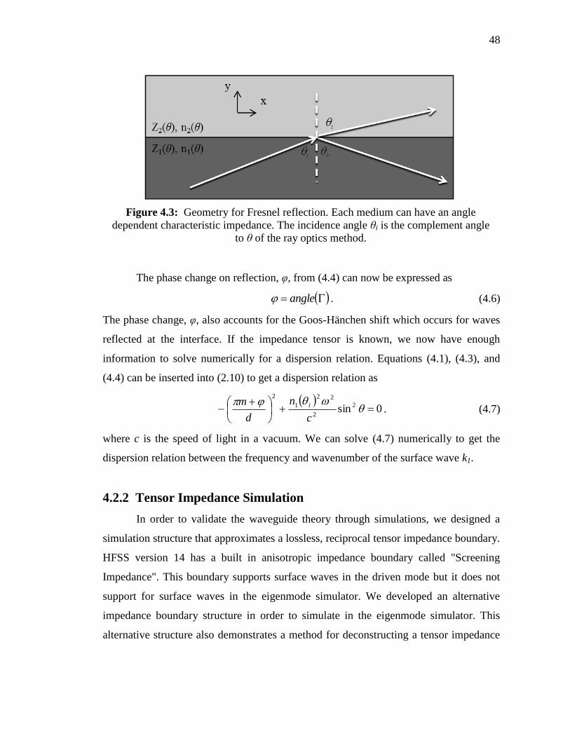
48
The phase change on reflection, φ, from (4.4) can now be expressed as
angle . (4.6)
The phase change, φ, also accounts for the Goos-Hänchen shift which occurs for waves
reflected at the interface. If the impedance tensor is known, we now have enough
information to solve numerically for a dispersion relation. Equations (4.1), (4.3), and
(4.4) can be inserted into (2.10) to get a dispersion relation as
0sin 2
2
22
1
2
c
n
d
m i. (4.7)
where c is the speed of light in a vacuum. We can solve (4.7) numerically to get the
dispersion relation between the frequency and wavenumber of the surface wave k1.
4.2.2 Tensor Impedance Simulation
In order to validate the waveguide theory through simulations, we designed a
simulation structure that approximates a lossless, reciprocal tensor impedance boundary.
HFSS version 14 has a built in anisotropic impedance boundary called "Screening
Impedance". This boundary supports surface waves in the driven mode but it does not
support for surface waves in the eigenmode simulator. We developed an alternative
impedance boundary structure in order to simulate in the eigenmode simulator. This
alternative structure also demonstrates a method for deconstructing a tensor impedance
Figure 4.3: Geometry for Fresnel reflection. Each medium can have an angle
dependent characteristic impedance. The incidence angle θi is the complement angle
to θ of the ray optics method.

49
surface into multiple scalar elements. A unit cell of our proposed model for a tensor
impedance surface is shown in Figure 4.4. More recent versions of HFSS (starting with
version 15) have implemented the tensor impedance boundary for the eigenmode solver.
Therefore, these newer versions do not require a new unit cell to model tensor
impedance surfaces. However, the following analysis shows that a tensor impedance
surface can still be modeled using scalar boundary conditions.
The unit cell consists of four ideal scalar boundaries: perfect electric conductor
(PEC), perfect magnetic conductor (PMC), and two isotropic impedance boundaries
which are labeled Zxx and Zyy in Figure 4.4. An arbitrarily large surface can be
constructed by repeating the unit cell in two dimensions. The size of the cell must be
small compared to the wavelength being tested. In the actual implementation, the PEC
had to be replaced with a finite conductivity boundary because the HFSS eigenmode
simulator does not allow a periodic boundary to be in contact with both an impedance
and PEC boundary. The difference between the PEC and finite conductivity boundaries
was a negligible decrease in conductivity from 1e30 S/m to 1e29 S/m.
For small cell sizes the checkerboard can be modeled in the long wave limit, and
the effective surface impedance can be obtained by averaging over the cells for a
specific wave direction. For a wave propagating in the x-direction, the PEC and Zxx
boundaries are in series and average to a surface of Zxx/2 since the surface impedance of
PEC is zero. The Zyy and PMC boundaries are also in series and average to infinity since
Figure 4.4: Checkerboard structure. The structure can be simulated to approximate
a tensor impedance surface boundary. The structure has two isotropic impedance
surface boundaries labeled Zxx and Zyy.

50
the surface impedance of PMC is infinity. Averaging Zxx/2 and infinity in parallel using
the harmonic mean gives an X-direction impedance of Zxx. For a wave propagating in
the y-direction, the same analysis gives an impedance of Zyy. Near field effects occur
immediately above the checkerboard surface and result in a complicated field profile.
Above the boundary at a length on the order of the unit cell size or greater, the ratio of
the electric and magnetic fields equals the effective impedance that is solved from the
previous description. This is a reason why the unit cell must be small with respect to the
wavelength. There are two different impedances in the principal directions that can be
obtained using the averaging method. Simulations are performed to verify that these
principal-direction impedances are modeled correctly using the long-wave limit and to
verify that hybrid modes are supported at intermediate angles.
A surface that correctly models a dispersion-free tensor impedance surface
boundary must satisfy two conditions. First, the impedance on the surface must be
constant with respect to frequency. Preferably for this surface, the impedances of the X-
and Y-directed waves are equal to the input values of Zxx and Zyy. Second, the surface
must have the correct impedance vs. propagation direction relation as defined by (2.9).
To verify the two conditions, the checkerboard structure was simulated in HFSS using
the structure as shown in Figure 4.5. The eigenmode simulator is used to solve for the
dispersion of an infinite checkerboard lattice. Simulating over a single unit cell or
multiple cells (Figure 4.5 shows an 8x8 lattice) has no effect on results. This is expected
because regardless of the number of unit cells tested, the simulator models an equivalent
infinite structure.

51
Propagation along the principle directions of two lattices was simulated and the
resulting wave impedances are shown in Figure 4.6. The simulated impedance is
obtained from the ratio of the longitudinal electric field and the transverse magnetic
field. For both lattices the wave impedance matches the input values over a wide
frequency range. At higher frequencies the simulated surface impedance varies by
approximately 2% from the desired value. If the lattice size is increased from 0.1mm (as
shown) to 0.2mm, the maximum error rises to around 6% in this frequency range. In
general, increasing the unit cell size causes increased dispersion. Arbitrarily small errors
can be obtained by shrinking the size of the lattice, at the cost of increased simulation
time. The Zxx curve in Figure 4.6 shows that the impedance rises at low frequencies.
This is due to the chosen height of the vacuum simulated above the impedance surface.
We used PEC for the top boundary in this model to improve simulation convergence,
but this can cause errors if significant wave power is present at the top of the structure.
Increasing the box height eliminates the effect of the top boundary. In general, as the
desired frequency range is lowered, a taller box is needed to properly determine the
Figure 4.5: Simulation structure in HFSS for checkerboard surface. The lattice is
repeated multiple times over two dimensions. The eigenmode simulator finds
dispersion results for an infinite lattice. The height of the air box above the surface is
not to scale.

52
impedance. Low impedance values also require a larger box because fields are more
loosely confined. By choosing a sufficient box height and shrinking the unit cell to the
necessary size, the effective scalar impedance of the checkerboard structure can be
arbitrarily constant with respect to frequency.
Along with having dispersion free impedance, tensor impedance surfaces must
respond correctly for wave propagation at any angle. Figure 4.7 shows the simulated and
theoretical impedance as a function of propagation direction for the two lattices
discussed above. For both cases in Figure 4.7, the theory and simulation match very
closely. This shows that the propagation characteristics and field decay above the
checkerboard matches the theory for hybrid TM-like modes. Therefore, we now have
shown that an appropriately designed checkerboard structure correctly models a tensor
impedance surface.
Figure 4.6: Impedance vs. frequency. The waves propagate in the X- and Y-
directions. Two different Y (propagating) direction impedances were tested,
Zyy=j399 Ω and Zyy= j1330 Ω. All other parameters were identical in both
simulations: unit cell length=0.1mm, Zxx= j133 Ω, and vacuum height=45mm.
0 10 20 30 40 500
200
400
600
800
1000
1200
1400
X: 1.416
Y: 1333
Frequency (GHz)
Impedance (
j )
X: 12.56
Y: 1354
X: 3.566
Y: 400.5
X: 31.8
Y: 407.5
X: 4.87
Y: 142
X: 44.05
Y: 136.2
Zxx
Zyy=j399
Zyy=j1330

53
4.2.3 Anisotropic Waveguide Results
We modeled anisotropic waveguides using the eigenmode solver in HFSS. An
inner guiding section was constructed using the checkerboard structure discussed in the
previous section. The outer region used an isotropic impedance boundary condition as
shown in Figure 4.8. Periodic boundary conditions were used to solve for the dispersion
relation of surface waves propagating along the guiding region.
Figure 4.7: Effective scalar impedance vs. propagation direction. The simulation is
from a checkerboard structure with dispersion results shown in Figure 4.6.
Impedance was simulated for multiple rotation angles. The theoretical solution is
obtained from (2.9). For the theory, Zxx and Zyy values at 10GHz from Figure 4.6
were used. For both anisotropy levels, the theoretical angle-dependence of
impedance matched the simulated result.
0 20 40 60 800
200
400
600
800
1000
1200
1400
Rotation (degrees)
Impedance (
j )
Equation (2.9)
Checkers Simulation
Equation (2.9)
Checkers Simulation

54
Two guides were tested, one with low anisotropy and another with higher
anisotropy. Figure 4.9 shows the magnitude of the electric field for the lowest three
modes in the lower anisotropy guide. Multiple modes can be supported in the guide as
described in (4.4) and (4.7). Fields are bounded to the surface and concentrated within
the guiding region. The fields have sinusoidal variation within the guide and decay
exponentially outside and above the guide surface. No power leaks away at the guide
edges, and the wave is transmitted without losses.
Figure 4.8: Simulation structure of the checkerboard guide. The guide interior is an
anisotropic checkerboard surface. The exterior region is an isotropic scalar surface
Z2=j133Ω. The guide drawing is not to scale. The details of the checkerboard are re-
plotted (another version is also shown in Figure 4.4). The vacuum height above the
surface is 45mm, and the unit cell size is 0.1mm by 0.1mm. The width of each guide
was set to 18mm which required 180 unit cells (only 12 unit cells are shown in the
figure).

55
The dispersion relations for the two guides are shown in Figure 4.10. Figure
4.10a shows that in the low anisotropy case, the theory matches the simulation well for
the lowest three modes of the guide. For any mode, the frequency must lie below the
line labeled “Outer Region.” This is the dispersion relation for a surface wave on a
uniform surface with impedance equal to that of the region outside the guide. Since the
outer region has a lower impedance than the interior, it represents the highest possible
frequency-wavenumber ratio in the structure. For the higher anisotropy case shown in
Figure 4.10b, the simulation and theory deviate somewhat, especially for the higher
modes. The deviation is caused by the increased fraction of TE field components in the
Figure 4.9: Magnitude of the electric field. The lowest three modes of the guide are
shown (logarithmic scale). The structure is a checkerboard structure with
Zprop=j399Ω and Ztrans=j133Ω. The field has sinusoidal variation within the guide
and exponential decay above and outside the guide. The high-impedance guiding
region is bounded by the dotted line shown in each figure.

56
mode on the high-anisotropy surface. Figure 2.2 shows the fraction of TE field in the
mode for the low and high anisotropy cases. The TE component of the hybrid mode is
not supported by the isotropic TM surface that bounds the guide. In order to simplify the
theory, a single TM surface wave ray was used to match these components as shown in
Figure 4.3 and described in Section 4.2.1. The single TM ray is set to the effective
impedance of the tensor surface, but this does not perfectly model the interaction at the
edge of the guide. In reality there is a discontinuity in the mode since the interior region
contains a TM-TE hybrid mode and the exterior region is a pure TM mode. This
discontinuity can induce plane wave scattering into the surrounding space and is
difficult to model. However, the results show that the simple ray optics model is still
sufficient to roughly predict the dispersion relation for a highly-anisotropic tensor
impedance guide.

57
(a)
(b)
Figure 4.10: Frequency vs. wavenumber plot for a checkerboard guide. The tensor
impedance is Ztrans=j133Ω and (a) Zprop=j399Ω, (b) Zprop=j1330Ω. The simulated
points are shown as circles. The theory line is the response as predicted from the ray-
optics method. The line labeled Outer Region represents the dispersion relationship
of a surface wave on a uniform surface with Z2=j133Ω. This is the (isotropic)
impedance of the region outside the guide.
0 200 400 600 800 10000
5
10
15
20
25
30
35
40
k (m-1)
Fre
quency (
GH
z)
Simulation
Theory
Outer Region
0 200 400 600 800 10000
5
10
15
20
25
30
k (m-1)
Fre
quency (
GH
z)
Simulation
Theory
Outer Region
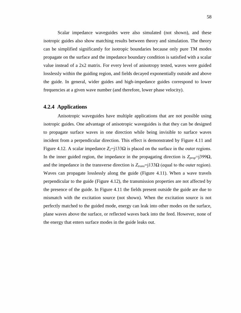
58
Scalar impedance waveguides were also simulated (not shown), and these
isotropic guides also show matching results between theory and simulation. The theory
can be simplified significantly for isotropic boundaries because only pure TM modes
propagate on the surface and the impedance boundary condition is satisfied with a scalar
value instead of a 2x2 matrix. For every level of anisotropy tested, waves were guided
losslessly within the guiding region, and fields decayed exponentially outside and above
the guide. In general, wider guides and high-impedance guides correspond to lower
frequencies at a given wave number (and therefore, lower phase velocity).
4.2.4 Applications
Anisotropic waveguides have multiple applications that are not possible using
isotropic guides. One advantage of anisotropic waveguides is that they can be designed
to propagate surface waves in one direction while being invisible to surface waves
incident from a perpendicular direction. This effect is demonstrated by Figure 4.11 and
Figure 4.12. A scalar impedance Z2=j133Ω is placed on the surface in the outer regions.
In the inner guided region, the impedance in the propagating direction is Zprop=j399Ω,
and the impedance in the transverse direction is Ztrans=j133Ω (equal to the outer region).
Waves can propagate losslessly along the guide (Figure 4.11). When a wave travels
perpendicular to the guide (Figure 4.12), the transmission properties are not affected by
the presence of the guide. In Figure 4.11 the fields present outside the guide are due to
mismatch with the excitation source (not shown). When the excitation source is not
perfectly matched to the guided mode, energy can leak into other modes on the surface,
plane waves above the surface, or reflected waves back into the feed. However, none of
the energy that enters surface modes in the guide leaks out.

59
Figure 4.11: Anisotropic waveguide with wave propagating in the guide. Wave
power outside the guide is due to mismatch between the feed mode and the guide
mode.
Figure 4.12: Anisotropic waveguide at orthogonal incidence. The wave does not
interact with surface wave incident from a perpendicular direction. The guide
structure is identical to that of Figure 4.11.

60
Next we will demonstrate the ability to arbitrarily set phase velocity, vp, and
group velocity, vg, in an anisotropic surface waveguide. The phase and group velocities
are defined as ω/k and ∂ω/∂k respectively, where k is the surface wavenumber. For a
given impedance tensor and guide width, vp and vg can be calculated numerically from
the dispersion relation (4.7). Figure 4.13 shows that there are multiple impedance
tensors to implement a desired vp for a given frequency and fixed guide width. Each of
these impedance tensors has different vg. The guide is oriented along a major axis of the
impedance tensor, and the tensor is therefore diagonal. Dispersion curves for the
impedance tensors labeled in Figure 4.13 are shown in Figure 4.14. The dispersion
curves cross at f0=10 GHz, and vp=0.8c at this point. Only one value of vg can be
obtained using an isotropic surface impedance. Anisotropy allows vp and vg to be set
independently. Similarly, by using tensor impedances, vp and vg can be held constant as
the guide width is swept.
Figure 4.13: Impedance tensor values for constant phase velocity. The guide has
width d=10mm, f0=10GHz, outer region impedance Z2=j133Ω, and desired phase
velocity vp=0.8c. Off-diagonal impedance tensor values are set to zero. The isotropic
value of the curve is at Zprop=Ztrans=j502.4Ω. Dispersion curves for the labeled
tensors are plotted in Figure 4.14.
200 400 600 800 1000 1200 1400 1600200
300
400
500
600
700
800
900
1000
X: 1600
Y: 257.5
Ztrans
(j)
Zpro
p (
j )
X: 900
Y: 339.6
X: 500
Y: 504.2
X: 350
Y: 683.3
X: 250
Y: 960.6

61
Figure 4.15 shows the tensors that give a desired vp and vg for a range of guide
widths. The propagating impedance remains fairly constant, and transverse impedance
declines as the width of the guide increases. The dispersion curves for the tensors
labeled in Figure 4.15 are shown in Figure 4.16. The dispersion curves are nearly
identical for each tensor, and the plots lie overlaid on each other such that only one line
is clearly visible over the entire range. Since the tensors have the same dispersion
relation, each tensor will have equal vp and vg at any frequency. However, both vp and vg
change with frequency.
Figure 4.14: Dispersion plots for constant phase velocity. The guide has width
d=10mm and outer region impedance Z2=j133Ω. The impedance values give a phase
velocity of 0.8c at 10GHz. The dispersion curves cross at 10 GHz giving identical
phase velocities. The group velocity is the slope of the dispersion curve at this point.
0 200 400 600 800 10000
2
4
6
8
10
12
14
16
18
20
k (m-1)
Fre
quency (
GH
z)
Z1prop
=960.6 Z1trans
=250
Z1prop
=683.3 Z1trans
=350
Z1prop
=502.4 Z1trans
=502.4
Z1prop
=339.6 Z1trans
=900
Z1prop
=257.5 Z1trans
=1600
240 260 280
9.5
10
10.5
k (m-1)
Fre
quency (
GH
z)
f0=10GHz, v
p=0.8c, d=10mm
Z1prop
=960.6 Z1trans
=250
Z1prop
=683.3 Z1trans
=350
Z1prop
=502.4 Z1trans
=502.4
Z1prop
=339.6 Z1trans
=900
Z1prop
=257.5 Z1trans
=1600

62
Figure 4.15: Impedance tensor values for vp = 0.8c and vg = 0.65c. The
solution is for f0=10GHz, and outer impedance Z2=j133Ω. Dispersion plots for the
labeled tensors are shown in Figure 4.16.
Figure 4.16: Dispersion plots for the tensors labeled in Figure 4.15. The tensors
were solved such that vp=0.8c and vg=0.65c at f0=10GHz and outer impedance
Z2=j133Ω. The tensors have nearly identical dispersion curves and the plots lie
overlaid on each other. Therefore, these tensors will have equal vp and vg at any
frequency (although the desired values of vp = 0.8c and vg = 0.65c will only occur at
f0=10GHz).
5 10 15 20200
400
600
800
1000
1200
1400
X: 15
Y: 401
Guide Width d (mm)
Z1 (
j )
X: 10
Y: 400X: 5
Y: 344
X: 20
Y: 216
X: 15
Y: 405
X: 20
Y: 404
X: 10
Y: 690
X: 5
Y: 1.37e+003
Z1prop
Z1trans
0 100 200 300 400 500 6000
5
10
15
20
k (m-1)
Fre
quency (
GH
z)
d=5mm Z1prop
=344 Z1trans
=1370
d=10mm Z1prop
=400 Z1trans
=690
d=15mm Z1prop
=405 Z1trans
=401
d=20mm Z1prop
=404 Z1trans
=216
Outer Region

63
Using the theory, three surface waveguide structures were simulated in HFSS
with the results shown in Figure 4.17. The left-most guide has a constant width of
20mm. The center guide has a varying width from 5-20mm in an hourglass shape. The
impedance of this guide is varied so that the phase and group velocity remains constant
and identical to the constant-width guide. The far right guide has the same hourglass
shape but with a constant impedance identical to the straight guide. Figure 4.17 shows
the electric field component normal to the surface where light is positive values and
dark is negative values. Black lines are added in order to compare the phase fronts in
each guide. We can see that the constant width guide and the hourglass guide with
correctly chosen impedance have the same phase fronts over the entire length of the
guide. The hourglass guide with constant impedance has phase fronts different from the
others. The impedance of the left guide is set so that vp=0.8c and vg=0.65c. In the center
guide, the range of vp is from 0.798-0.802c, and the range of vg is from 0.62-0.68c.
Errors are caused by approximations in the theory and simulations as described below.

64
The impedance values in the simulation were adjusted from the theory in order
to obtain optimal simulated results. These adjustments account for errors in ray optics
theory and assumptions made to simplify the waveguide dispersion equations. The
narrow waveguide sections required the largest modifications. The theoretical
impedance tensor values for these structures are plotted in Figure 4.15. Impedances
were adjusted from their theoretical values to ensure that vp=0.8c. By focusing
specifically on vp, vg deviates from its desired value of 0.65c. However, an exhaustive
search of impedance tensors would allow arbitrarily accurate vg solutions.
Figure 4.17: Anisotropic waveguides with propagating waves in the guides. In each
case the outer impedance is Z2=j133Ω, the guiding region is 300mm, the air height is
100mm, and the width outside is 100mm (not shown to scale).
65
4.2.5 Conclusion
A simple theoretical model for an impedance surface waveguide was developed
using a ray optics method and tensor impedance surface theory. A unit cell was also
designed in HFSS that can model tensor impedance surfaces. This unit cell was used to
simulate a novel tensor surface impedance waveguide structure. The simulations
matched the theory over a wide range of tensors and over multiple propagation modes.
Two applications of anisotropic waveguides were investigated. In one example, an
anisotropic waveguide was able to guide waves in one direction and let them pass
through in another. In a second example, a guide had its width changed but it maintains
constant phase velocity and group velocity. In future work we plan to extend surface
waveguide theory to real tensor impedance surfaces formed from metal patches
patterned on grounded dielectric substrates. In these structures, the theory still applies,
but frequency dependent surface impedances must be accounted for. Waveguides with
TM guiding regions and TE exterior regions could be investigated as well.
4.3 Realized Artificial Tensor Impedance Waveguides
In this section, a tensor impedance surface waveguide, as analyzed in Section 4.2
is realized. An idealized illustration of a transparent waveguide is shown in Figure 4.18.
The impedance surface is built as a printed circuit. These structures are created by
patterning metal on the top layer of a grounded dielectric slab. The waveguide is
designed with square and rectangular unit cells as shown in Figure 4.19. These unit cells
have been analyzed along their principal axes [33]. Further analysis of printed circuit
tensor impedance surfaces has also been performed, and it was found that tensor
impedance boundaries do not always accurately model printed structures, and more-
accurate models have been proposed [26, 27, 44]. However, currently these methods can
only be applied to individual unit cells, and not large structures like waveguides. In
order to confirm the accuracy of the ideal tensor impedance model, we have compared
this ideal model to simulations of printed circuit structures and measurement.
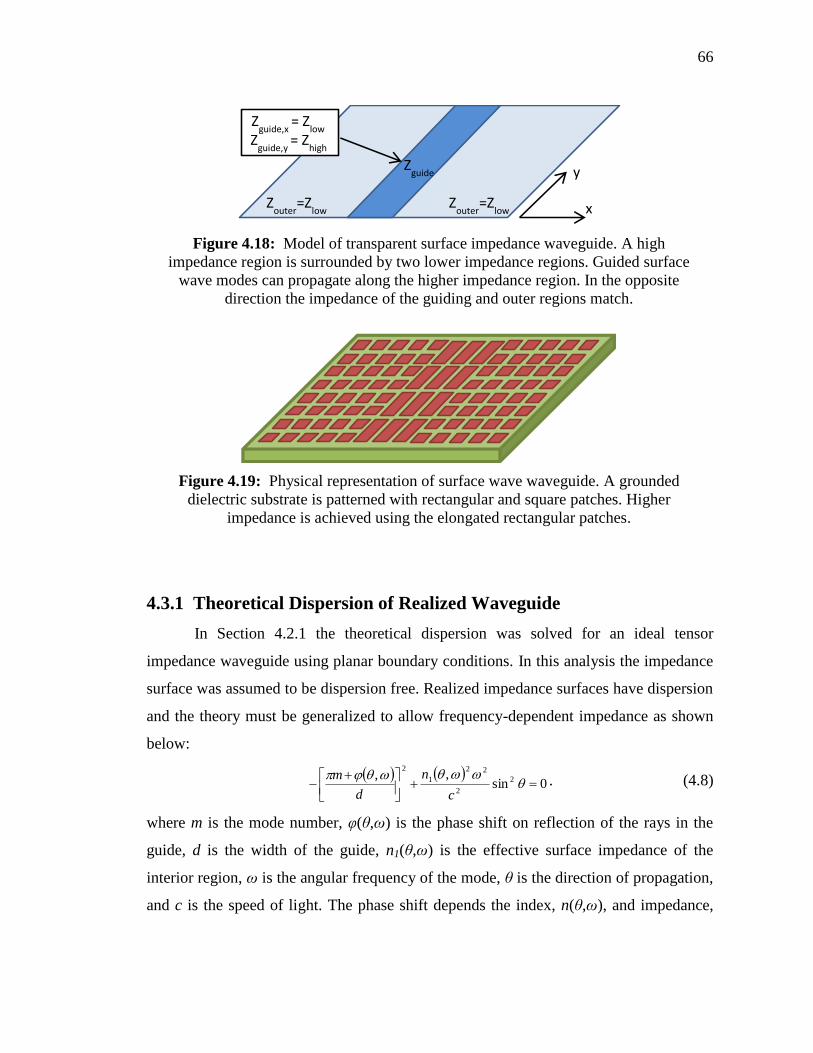
66
4.3.1 Theoretical Dispersion of Realized Waveguide
In Section 4.2.1 the theoretical dispersion was solved for an ideal tensor
impedance waveguide using planar boundary conditions. In this analysis the impedance
surface was assumed to be dispersion free. Realized impedance surfaces have dispersion
and the theory must be generalized to allow frequency-dependent impedance as shown
below:
0sin
,, 2
2
22
1
2
c
n
d
m . (4.8)
where m is the mode number, φ(θ,ω) is the phase shift on reflection of the rays in the
guide, d is the width of the guide, n1(θ,ω) is the effective surface impedance of the
interior region, ω is the angular frequency of the mode, θ is the direction of propagation,
and c is the speed of light. The phase shift depends the index, n(θ,ω), and impedance,
Figure 4.18: Model of transparent surface impedance waveguide. A high
impedance region is surrounded by two lower impedance regions. Guided surface
wave modes can propagate along the higher impedance region. In the opposite
direction the impedance of the guiding and outer regions match.
Figure 4.19: Physical representation of surface wave waveguide. A grounded
dielectric substrate is patterned with rectangular and square patches. Higher
impedance is achieved using the elongated rectangular patches.
x
y
Zguide,x = Z
low
Zguide,y
= Zhigh
Zguide
Zouter
=Zlow
Zouter
=Zlow

67
Z(θ,ω), of the interior and exterior regions of the guide. The surface impedance is
frequency dependent, but when applying the theory, a harmonic excitation is assumed.
Therefore, the dispersion relation is solved independently at each frequency, and single
impedance tensor is used for each solution.
To apply the theoretical model, the frequency dependent impedance, Z(θ,ω)
must be known ahead of time, along with the corresponding index n(θ,ω). In this paper,
the rotation and frequency dependence of the unit cells are determined by simulation
and these values are applied to the theoretical model. These simulations are described
below in Section 4.3.2. Along with frequency dispersion, realized impedance surface
exhibit spatial dispersion. This phenomena has been analyzed for patch-type unit cells
with no vias [26, 27]. Spatial dispersion implies an inconsistency between the predicted
anisotropy as defined by (2.9), and the actual anisotropy of the unit cell. This
inconsistency causes errors in Z(θ,ω) and n(θ,ω), but it will be shown in Sections 4.3.2
and 4.3.3 that ideal theory can still accurately model the waveguide dispersion.
4.3.2 Unit Cell Analysis
The unit cells for the waveguide used a 1.27mm thick Rogers 3010 substrate (for
simulations we used the design dielectric constant εr = 11.2). This substrate has the
highest dielectric constant of commonly available printed circuit board materials, and
the largest standard thickness. Higher dielectric constants and larger thickness have been
shown to allow broader bandwidth anisotropy [52]. The dimensions of the rectangular
unit cell for the guiding region are shown in Figure 4.20a, and the isotropic unit cell for
the outer region is shown in Figure 4.20b. Both unit cells have gaps between the metal
patch and the edge of the unit cell that are identical on all four sides.

68
Figure 4.21 shows the dispersion relation of each unit cell for waves traveling
along the principal axes of the cell. The dispersion was simulated using the eigenmode
solver of Ansys HFSS version 15. Surface impedance curves are shown in Figure 4.22.
For the isotropic 1x1mm unit cell, the impedance along the two principal axes is
identical because the unit cell is square. The 2x1mm unit cell has different impedance
for each axis. The impedance along the 1mm dimension of the rectangular cell is nearly-
identical to the 1x1mm unit cell (as also demonstrated in [33]). The fact that the square
unit cell and the short direction of the rectangular unit cell have the same surface
impedance is what allows the waveguide to be transparent in orthogonal directions. The
larger impedance along the propagating direction of the rectangular unit cell allows
waveguide modes to be confined to the interior region
Figure 4.20: Unit cell dimensions. The illustrations are for (a) anisotropic unit cell
and (b) isotropic unit cell. For both unit cells the substrate is a grounded dielectric
with a metal patch. The patch is represented by the inner rectangle, and the distance
between the patch and the unit cell edge is g=0.2mm on all sides. The anisotropic
unit cell is of 2x1mm and the isotropic unit cell is 1x1mm.

69
Figure 4.21 and Figure 4.22 show anisotropic behavior for the principal axes of
the 2x1mm unit cell, but it is also necessary to verify the performance of the unit cell for
waves propagating at directions between the principal axes. For ideal tensor impedance
boundary conditions the dispersion for the principal axes is sufficient to calculate the
dispersion at any other angle. However, on realized surfaces, spatial dispersion [26, 27],
Figure 4.21: Dispersion relation for anisotropic and isotropic unit cells. The low
impedance direction of the anisotropic unit cell has nearly identical dispersion to the
isotropic unit cell. In the high impedance direction is lower in frequency at any given
wavenumber.
0 200 400 600 800 1000 1200
8
10
12
14
16
18
20
Fre
quency (
GH
z)
k (m-1)
2x1mm Low Z
2x1mm High Z
1x1mm
Light
Figure 4.22: Surface impedance vs. frequency. The results are for the principal
directions of anisotropic and isotropic unit cells. The low impedance direction of the
2x1mm unit cell has the same impedance relation as the 1x1mm unit cell.
8 10 12 14 16 18 200
200
400
600
800
1000
Frequency (GHz)
Z (
j )
2x1mm Low Z
2x1mm High Z
1x1mm

70
and mode interference [52], can distort propagation between the principal axes. The
dispersion relation for multiple propagation directions has been simulated for both
isotropic and anisotropic unit cells. Isofrequency index contours for the isotropic unit
cell are shown in Figure 4.23a. For the isotropic unit cell the contours are circular
because the index has the same value for any propagation direction.
Isofrequency contours for the 2x1mm unit cell are shown in Figure 4.23b.
Results from simulation are plotted as dots. Theoretical curves are shown as solid lines,
and are calculated using the results of the principal axis simulations at each frequency.
The principal axes are oriented along the x- and y- axes where the x-axis (high
impedance) corresponds to a wave propagating along the 2mm dimension of the unit
Figure 4.23: Isofrequency impedance contours. The results are for (a) isotropic unit
cell and (b) anisotropic unit cell. The radial direction is effective index and the theta
direction is the direction of propagation. Theoretical curves are shown as solid lines
and simulations are the dots. The legend labels different frequencies with units of
GHz. The contours are symmetric across the x- and y-axis so only the first quadrant
is plotted. Ten rotations from 0-90° are simulated.
0 0.5 1 1.50
0.5
1
1.5
(a)
15
14
13
12
11
10
9
8
7
0 0.5 1 1.5 2 2.50
0.5
1
1.5
2
(b)
15
14
13
12
11
10
9
8
7

71
cell and the y-axis (low impedance) corresponds to the 1mm dimension. At low
frequencies the ideal theory and simulation match but as frequency increases the
simulation deviates from the theory. The cutoff of the TE mode is at 12.3 GHz, and it
has been shown that this is where the ideal tensor impedance theory is no longer valid
[52]. Above the cutoff frequency the simulation rapidly deviates from the theory with
the worst estimation generally occurring around a propagation angle of 45°. At 12 GHz,
13GHz, 15 GHz, the index is off by 6%, 12%, and 15% respectively for a wave
propagating at 45°. This error is similar at higher frequencies but other angles begin to
have large error also due to mode distortion.
Although the unit cell dispersion curve deviates from the simple single-mode
theory, especially above the TE cutoff at 12.3GHz, the guide is oriented along the
principal axis of the unit cell. In this orientation, the wave is propagating along the
direction that does not deviate as significantly from the theory. In Section 4.3.3, it is
found in both simulation and experiment that the waveguide operates above 12.3 GHz
consistently with impedance surface theory.
4.3.3 Waveguide Dispersion and Fields
The dispersion of a waveguide is tested using measurement, simulation, and the
theoretical model. For each case, the width of the waveguide is set to d=10mm. In
general, wider guides bend the dispersion relation to lower frequencies, and lower the
cutoff frequency of higher order waveguide modes.
A. Measured Dispersion Setup
A surface wave waveguide was constructed using the unit cells analyzed in
Section 4.3.2. The total size of the board was 16×10 inches and the waveguide was 16
inches long centered on the board with a 10mm wide guiding region (10 unit cells
wide). A photograph of a section of the waveguide is shown in Figure 4.24. A near field
scanner was used to make the dispersion measurement. The dispersion was obtained
from the phase velocity of the mode in the waveguide. The measurement setup is shown
in Figure 4.25. The feed is a trapezoidal sheet of Rogers 5880. An end-launch SMA

72
adapter is attached to the back of the feed and leads to one port of an Agilent E5071C
Vector Network Analyzer (VNA). The second port of the VNA is attached to a probe
that is scanned across the surface. The probe tip is 5mm long and oriented vertically
approximately 2mm above the surface. For dispersion measurements the probe is
scanned along the center of the guide at 200μm increments. At each position, S21 phase
is measured by the VNA, and this data is used to calculate phase velocity. The effective
surface index is calculated from the phase velocity, and this index is used to derive the
dispersion of the waveguide
The feed does not couple perfectly into the guided surface mode and some power
Figure 4.24: Photograph of tensor impedance surface waveguide.
Figure 4.25: Measurement setup for waveguide. Magnetic absorbers are place to
the sides of a trapezoidal feed. A vertical probe is located in the upper right side of
the photograph. Photograph of tensor impedance surface waveguide.

73
is reflected or launched as surface waves in the outer region. However, waves excited
into a guided mode do not spill outside the guiding region, and the feed is designed so
that minimal fields are excited outside of the waveguide mode at the center of the
operating region. For printed circuit structures, other surface wave excitations have been
used such as a Yagi-like surface wave launcher [26, 27], and a flared microstrip line [4,
28]. These could allow better coupling efficiency into the waveguides. However, for this
study, the discrete trapezoidal surface wave launcher allowed the convenience of
moving the feed to launch a guided wave, or to launch waves at other positions or angles
on the surface. Two sheets of magnetic absorber (Arc-Tec DD11006) were placed on
either side of the feed to limit the amount of power reflected back into the guide from
the outer region. Both TM and TE modes are absorbed, and the modes are dissipated
both above and within the substrate. Magnetic absorber is also used to terminate the
guided mode and prevent reflections back into the guide. A well-matched surface wave
launcher could also be used to terminate the mode into a 50Ω load.
B. Simulated Dispersion Setup
The dispersion of the waveguide was simulated using the eigenmode solver in
Ansys HFSS version 15. The model used ideal tensor impedance boundary conditions.
Because of dispersion in the realized surface, the impedances are set differently for each
frequency as stipulated by Figure 4.22. The simulation setup is described in Section V
of [14], except this paper uses the anisotropic impedance boundary condition (instead of
the checkerboard structure), which has been implemented in the HFSS eigenmode
solver in the time since the previous publication. The waveguide simulation was
performed over the range where the unit cell was simulated: 7-20 GHz (as seen in
Figure 4.22). The impedance data was interpolated to obtain the values at 1 GHz
increments.
C. Theoretical Dispersion
The theoretical dispersion relationship is described by 4.8 and fully derived in
[14]. As noted in Section 4.3.1, the impedance of the unit cell must be solved before the
theoretical dispersion can be solved, and this impedance is dependent on both frequency
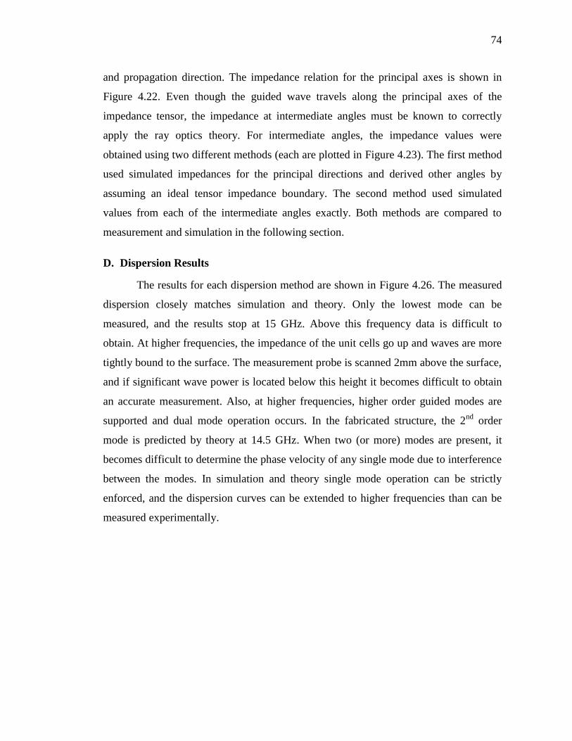
74
and propagation direction. The impedance relation for the principal axes is shown in
Figure 4.22. Even though the guided wave travels along the principal axes of the
impedance tensor, the impedance at intermediate angles must be known to correctly
apply the ray optics theory. For intermediate angles, the impedance values were
obtained using two different methods (each are plotted in Figure 4.23). The first method
used simulated impedances for the principal directions and derived other angles by
assuming an ideal tensor impedance boundary. The second method used simulated
values from each of the intermediate angles exactly. Both methods are compared to
measurement and simulation in the following section.
D. Dispersion Results
The results for each dispersion method are shown in Figure 4.26. The measured
dispersion closely matches simulation and theory. Only the lowest mode can be
measured, and the results stop at 15 GHz. Above this frequency data is difficult to
obtain. At higher frequencies, the impedance of the unit cells go up and waves are more
tightly bound to the surface. The measurement probe is scanned 2mm above the surface,
and if significant wave power is located below this height it becomes difficult to obtain
an accurate measurement. Also, at higher frequencies, higher order guided modes are
supported and dual mode operation occurs. In the fabricated structure, the 2nd
order
mode is predicted by theory at 14.5 GHz. When two (or more) modes are present, it
becomes difficult to determine the phase velocity of any single mode due to interference
between the modes. In simulation and theory single mode operation can be strictly
enforced, and the dispersion curves can be extended to higher frequencies than can be
measured experimentally.

75
Simulated and theoretical curves are shown up to 20 GHz for the first two
guided modes. The second mode has a cutoff when it intersects the dispersion curve of
the outer region. The outer region dispersion represents the highest phase velocity that
can be achieved in the guide, as this outer region has lower index than the interior
region. Two theoretical methods were used as described in the previous section. The
maximum difference in frequency between the two theories is less than 0.4GHz for
either mode (<3%). Therefore, results show that the simplified theory assuming an ideal
tensor impedance boundary is sufficient to predict the approximate dispersion relation.
The second method using the simulated impedances is slightly more accurate but
requires many more simulations
E. Field Profile of Guided Mode
The fields for the guided mode were measured and compared to simulation. The
Figure 4.26: Dispersion of guided modes in tensor impedance surface waveguide.
Only the lowest mode can be measured and this is shown as a solid line. The first
two modes are shown as dashed lines for the theoretical solutions, and as dots for
simulation. The first theory curve uses ideal tensor impedance theory to obtain
impedance at intermediate angles and the second theory curve uses simulation to get
these values. A black dashed line is the dispersion of light in a vacuum. Guided
modes must lie below the dispersion relation of the outer region, and this is shown as
a black line.
0 200 400 600 800 1000 12006
8
10
12
14
16
18
20
k (m-1)
Fre
quency (
GH
z)
Measurement
Theory 1
Theory 2
Simulation
Light
Guiding Cutoff
76
fields for ideal impedance boundary conditions were shown in [14]. A dispersive
structure using the rectangular unit cells is analyzed here. The model is constructed
identically to the experimental model with 10 unit cells across guiding region and 50
unit cells on across the isotropic region on each side. The electric field magnitude is
shown for the first two guided modes in Figure 4.27. The guiding region is marked as a
dashed line, and the mode is propagating into the page. The fields are most highly
concentrated between the patches. For both modes the field has sinusoidal variation
across the guiding region and exponential decay to the sides away from the guide. Field
decays exponentially above the substrate across the entire width of the structure.
Using the same experimental setup as for dispersion, a probe was scanned across
the guide orthogonal to the direction of propagation. The probe was again placed 2mm
above the surface and measurements were taken at 200μm increments. The power at
each point was measured at 12 GHz and this was transformed to a normalized field
magnitude which is plotted in Figure 4.28. An equivalent line from the simulation was
also plotted in Figure 4.28, and the normalized fields can be compared. Within the
guided region the simulated and measured responses are nearly identical and have a
sinusoidal profile. Outside the guide the field decays exponentially with distance. The
minor differences in field magnitude are likely due to the energy excited outside the
Figure 4.27: Normalized electric field magnitude. The plots show (a) 1st mode, and
(b) 2nd
mode for a simulation of a surface waveguide.
(a)
(b)

77
guide. Only the first mode can be measured in this manner because a pure second mode
cannot be experimentally excited. The impedance contrast between regions effects the
confinement of the mode with larger contrasts more closely confining modes to the
guiding region. Wider guides also have more mode confinement.
4.3.4 Near Field Measurements
Two-dimensional near field measurements were obtained using the setup
described in Section 4.3.3. The total size of the surface was 10×16 inches. The measured
area is slightly smaller than the total board size to allow space for the feed and absorbers
around the edge of the surface. The excitation source, shown in Figure 4.25, does not
couple perfectly into guided modes at all frequencies, and some power is excited
directly to the outer region. A vertical probe was swept 5mm above the surface along a
2mm grid. The probe was scanned higher above the surface for two-dimensional field
measurements because the surface was not completely flat and scanning lower could
cause contact between the probe and surface at the edges. Each measurement contains
about 25,000 points, and normalized field results at 11 GHz are shown in Figure 4.29.
Figure 4.28: Normalized electric field magnitude above waveguide.
-30 -20 -10 0 10 20 300
0.2
0.4
0.6
0.8
1
Position (mm)
Norm
aliz
ed F
ield
Magnitu
de
Measurement
Simulation
Guide Edges

78
Figure 4.29: Measured fields. The plots show normalized vertical (out of page)
electric field at 11 GHz for (a) guided mode, (b) orthogonal mode, and (c) angled
mode. Fields in (a), (b), and (c) are not plotted to the same scale.

79
A guided mode is displayed in Figure 4.29a. The mode is bound near the guide
and does not leak to the outer region. The measured bandwidth for guided modes is
from 9.4-15.2 GHz. Below 9.4GHz the measured mode is a regular surface wave (not
confined to the guiding region) because the impedance inside and outside the guide is
almost identical. At 11 GHz, as shown in Figure 4.29a, almost all of the fields are in the
waveguide mode and minimal fields are present in the outer region. Above 14 GHz, the
source excites more measurable fields in the outer region than as a guided mode. This is
because higher frequency modes have high impedance. High impedance modes are
tightly bound to the surface, and this is difficult to measure because the probe is scanned
5mm above the surface (in order to avoid scratching the material). At higher
frequencies, modes excited in the outer region (which still has lower impedance) are
measured much more easily because they are not as tightly bound. These outer-region
modes can reflect off the edges of the board and travel back across the waveguide
making it difficult to isolate the guided mode which exists mostly below the probe.
However, power that does enter as a guided mode does not leak away from the guide.
Figure 4.29b shows a two-dimensional field plot for a surface with a feed located
in the exterior region. The feed was a vertically-oriented monopole that excited semi-
circular phase fronts on the surface. The guiding and outer regions have identical
surface impedance for surface waves incident normal to the guide. Therefore, as seen in
Figure 4.29b, waves at normal incidence pass through the guide as if it were not present,
and transparency is confirmed. In this case, the wave front is only orthogonal directly
above the source. At off-normal angles, some reflections and distortion can be seen off
the guide. In Figure 4.29c the trapezoidal feed is used to launch a surface wave toward
the waveguide at a small grazing angle. In this case, the higher-impedance guiding
region reflects a significant portion of the incident power.
4.3.5 Curved Waveguide
A transparent curved waveguide was designed and measured, and Figure 4.30a
illustrates a schematic diagram for the surface. The outer region has small isotropic
surface impedance, analogous to Figure 4.18, and the guiding region is curved around a
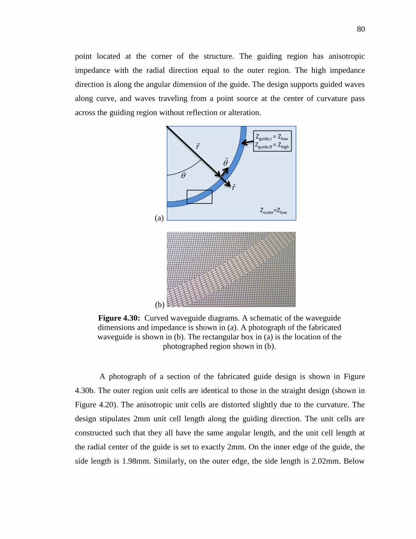
80
point located at the corner of the structure. The guiding region has anisotropic
impedance with the radial direction equal to the outer region. The high impedance
direction is along the angular dimension of the guide. The design supports guided waves
along curve, and waves traveling from a point source at the center of curvature pass
across the guiding region without reflection or alteration.
A photograph of a section of the fabricated guide design is shown in Figure
4.30b. The outer region unit cells are identical to those in the straight design (shown in
Figure 4.20). The anisotropic unit cells are distorted slightly due to the curvature. The
design stipulates 2mm unit cell length along the guiding direction. The unit cells are
constructed such that they all have the same angular length, and the unit cell length at
the radial center of the guide is set to exactly 2mm. On the inner edge of the guide, the
side length is 1.98mm. Similarly, on the outer edge, the side length is 2.02mm. Below
(a)
(b)
Figure 4.30: Curved waveguide diagrams. A schematic of the waveguide
dimensions and impedance is shown in (a). A photograph of the fabricated
waveguide is shown in (b). The rectangular box in (a) is the location of the
photographed region shown in (b).
Zguide,r = Zlow
Zguide,θ = Zhigh
r
r
Zouter=Zlow

81
20 GHz, simulation shows that the deviation from the surface impedance of a 2mm-long
unit cell is less than 1%. All unit cells are exactly 1mm in the radial direction. For the
outer region, the unit cells form a 1x1mm grid. These unit cells are removed in the
region where the guiding region intersects. As seen in Figure 4.30b, unit cells near the
edge of the guide are cut so there is no overlap between unit cells.
The width of the guiding region is 10mm, as was the case for the straight
waveguide. The radius from the center of curvature to the center of the waveguide was 8
inches. The substrate material and dimensions are the same as before, and near field
measurements were obtained from the same system used for the straight waveguides.
The guided mode was fed using the straight waveguide as a source. The trapezoidal feed
shown in Figure 4.25 fed the straight waveguide on one end, and the opposite was
pressed up to the curved waveguide. Figure 4.31a shows a guided mode at 11 GHz. This
was the frequency that had the best match between the trapezoidal feed and straight
waveguide mode. However, for the curved case the guided mode leaks into the outer
region. Figure 4.31b shows the same structure at 12 GHz. In this case there is minimal
leakage from the guided mode. The measured bandwidth for guiding without leakage is
from 11.7-15 GHz. Bending losses are analyzed in Section 4.3.6.
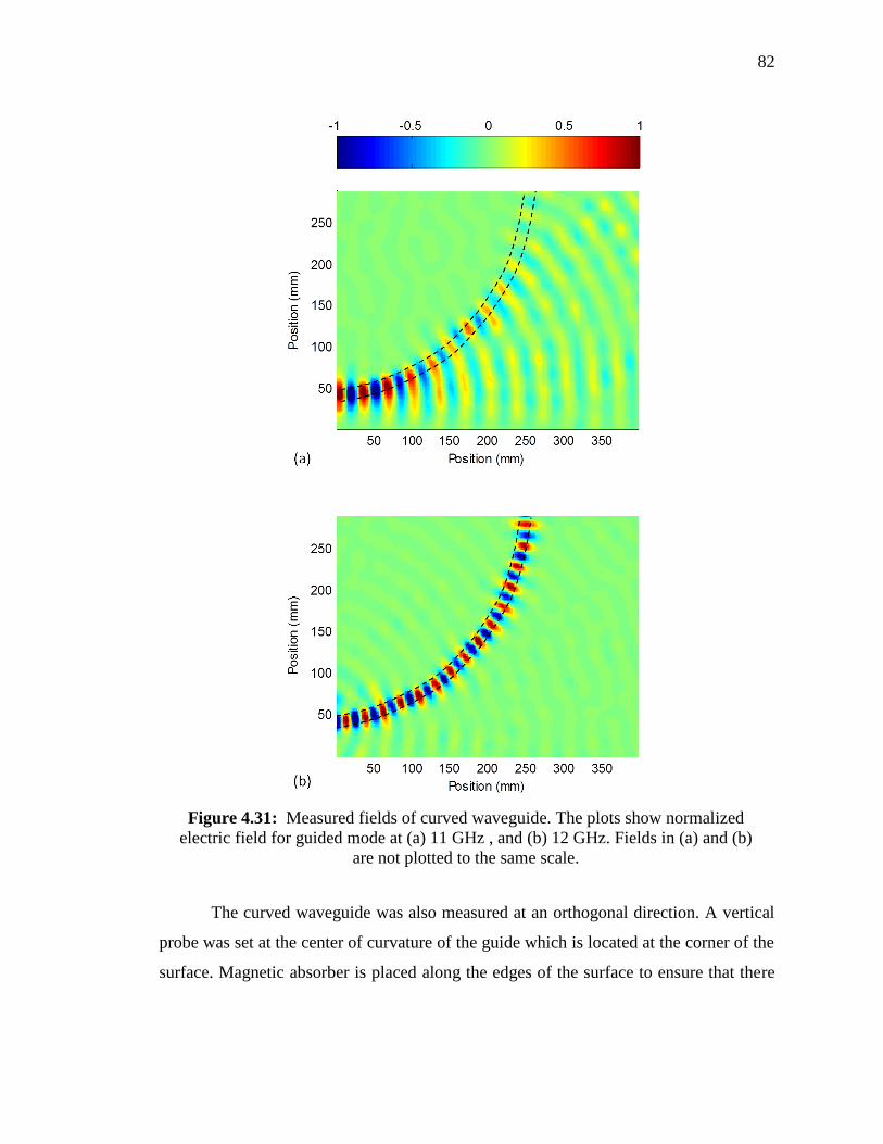
82
The curved waveguide was also measured at an orthogonal direction. A vertical
probe was set at the center of curvature of the guide which is located at the corner of the
surface. Magnetic absorber is placed along the edges of the surface to ensure that there
Figure 4.31: Measured fields of curved waveguide. The plots show normalized
electric field for guided mode at (a) 11 GHz , and (b) 12 GHz. Fields in (a) and (b)
are not plotted to the same scale.

83
are no reflections back into the surface. The source radiates circularly from the center of
curvature of the guide such that the wave is incident normally to the guide across the
entire structure. The field plot at 12 GHz is shown in Figure 4.32. The wave passes
through without reflection again confirming the transparency of the guided region. The
fields along the edges are reduced because magnetic absorber is placed along these
sides.
4.3.6 Analysis of Bending Loss
As mentioned in Section 4.3.5 and seen in Figure 4.31, the curved waveguide
exhibits bending loss that depends on the frequency, waveguide dimensions, and surface
properties. This phenomena also occurs for bending of dielectric slab and fiber
structures [53]. Leakage occurs at bends because the mode on the exterior of the curve
must travel faster than at the center in order to stay in phase. Leakage occurs where this
speed is larger than what can be supported by the materials. Ray optics has been used to
analyze dielectric slab waveguides and fibers to determine the bending loss of a
Figure 4.32: Measured field of orthogonally incident mode. The plot shows
normalized vertical electric field at 12 GHz.

84
multimode structure [54-57]. This method can be adapted for the surface wave
waveguide in order to predict the bending loss due to radiation from a curved
waveguide.
For straight waveguides, the ray optics guiding condition dictates that the rays
exhibit total internal reflection at the interface between the guiding region and the outer
region. This total internal reflection is frustrated by bending and curved waveguides
never exhibit total internal reflection [56]. However, the bending loss can be negligible
depending on the setup of the waveguide. The setup for the curved waveguide analysis
is shown in Figure 4.33. A straight waveguide of width 2ρ feeds a curved waveguide
with the same width and surface properties. The dispersion relation of this straight
waveguide is solved using (4.8), and the incidence angle of the ray in the straight
waveguide, θ, is obtained from this equation. The curved waveguide has a center radius
of R. The height of the ray crossing between the straight and curved sections is r. The
incidence angle at the inner and outer dimensions can be obtained geometrically as
follows [57]:
coscos 1
R
ri
, (4.9)
coscos 1
R
ro
. (4.10)
The incidence angle on the outer surface is always larger than on the inner surface. Rays
only lose power on the outer surface, and losses on the inner surface are negligible [56].
The angular dimension of the guide is ϕ, and Δϕ is the angular length between
successive reflections on the outer diameter.
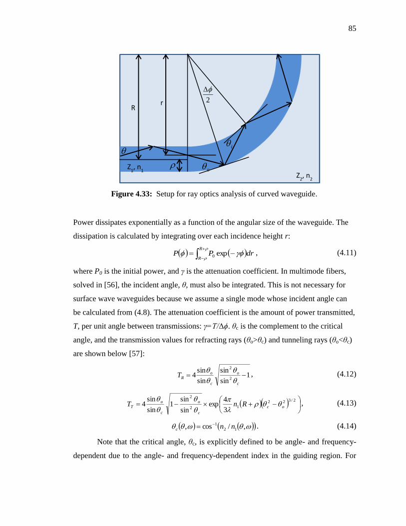
85
Power dissipates exponentially as a function of the angular size of the waveguide. The
dissipation is calculated by integrating over each incidence height r:
R
RdrPP exp0
, (4.11)
where P0 is the initial power, and γ is the attenuation coefficient. In multimode fibers,
solved in [56], the incident angle, θ, must also be integrated. This is not necessary for
surface wave waveguides because we assume a single mode whose incident angle can
be calculated from (4.8). The attenuation coefficient is the amount of power transmitted,
T, per unit angle between transmissions: γ=T/Δϕ. θc is the complement to the critical
angle, and the transmission values for refracting rays (θo>θc) and tunneling rays (θo<θc)
are shown below [57]:
1sin
sin
sin
sin4
2
2
c
o
c
oRT
, (4.12)
2/322
12
2
3
4exp
sin
sin1
sin
sin4 oc
c
o
c
o
T RnT
, (4.13)
,/cos, 12
1 nnc
. (4.14)
Note that the critical angle, θc, is explicitly defined to be angle- and frequency-
dependent due to the angle- and frequency-dependent index in the guiding region. For
Figure 4.33: Setup for ray optics analysis of curved waveguide.
Z2, n
2
Z1, n
1
r R
o
i
2

86
refracting rays, TR is the standard Fresnel relation. For tunneling rays, TT is solved using
a local plane wave analysis [56]. In [14] it was found that a true surface wave Fresnel
equation gave improved results for the phase on total internal reflection because it was
necessary to calculate the exact reflection phase shift (4.6). For losses due to bending we
have found that local plane wave analysis adequately predicts losses for the curved
surface wave waveguide.
Figure 4.34 shows the results for bending loss in the fabricated structure. The
measured data is calculated from the fields above the waveguide. The simulated curve
uses ideal tensor impedance boundaries with impedances as shown in Figure 4.22. The
theory curved is solved numerically from (4.11). Results show similar characteristics for
all three methods. In each case, minimal power is transmitted at low frequencies. At
high frequencies there is nearly-full power transmission for the simulated and theory
cases. The measured version shows some losses between 14-15 GHz. These losses are
due to bending loss of the second waveguide mode (which has a theoretical cutoff of
14.2 GHz and is not included in the theory), and material loss. Bending loss of the first
mode does not occur in this frequency range. This lossy section is also in the range
where the TM mode is distorted by the presence of TE modes. The theoretical model
closely predicts the frequency at which the structure no longer has nearly-complete-
guiding at 12.5GHz. However, the theory shows a steeper drop-off from nearly-
complete-guiding towards increased bending loss at lower frequencies.

87
The theory was used to predict the bending loss for different waveguide radii
using the same unit cells, and the results are shown in Figure 4.35. The half power
frequency is the frequency where the guide delivers half the power around the bend. The
theory predicts this location at 12.09 GHz for the fabricated structure as seen in Figure
4.34 and labeled explicitly in Figure 4.35 (note 20.32cm = 8 inches). As the center
radius, R, decreases the half power frequency increases. This is because higher
frequencies have larger impedance contrast, and R is electrically larger. On the right y-
axis the maximum transmitted power is plotted for each R. For R<0.75cm the
waveguide does not propagate 50% of the power at any frequency. The maximum
power output occurs about 0.5GHz above the half power frequency as seen in Figure
4.34.
Figure 4.34: Power loss over 90 degree bend on fabricated structure.
8 9 10 11 12 13 14 150
0.2
0.4
0.6
0.8
1
1.2
Frequency (GHz)
Pow
er
Ratio
Measured
Simulation
Theory

88
In the realized structure the impedance of the unit cell is dependent on
frequency. In order to show the effects of impedance and radius on propagation
independently, the theory was applied to a waveguide using ideal impedance boundary
conditions. The setup had guide width of 10mm, and outer region n=1.1. The index of
the inner region was swept from 1.2 to 2 (isotropic) for multiple radii. The results are
shown in Figure 4.36. For any given index value, increasing the radius decreases the
frequency where half the power is transmitted. Similarly, for a specific radius,
increasing the index decreases the frequency of half-power transmission.
Figure 4.35: Frequency of half-power loss vs. center radius of the waveguide. The
right axis shows the maximum power output from the waveguide.
0 5 10 15 20 25 3010
11
12
13
14
15
X: 20.32
Y: 12.09
Half
Pow
er
Fre
quency (
GH
z)
Center Radius (cm)
0 5 10 15 20 25 300.5
0.6
0.7
0.8
0.9
1
Max O
utp
ut P
ow
er
Ratio
Half Pow er Frequency
Max Output Pow er

89
4.4 Conclusion
We have demonstrated a simple application of tensor impedance surfaces in the
form of a waveguide that is transparent to surface waves in the orthogonal direction.
This can be extended to enable new applications such as antennas with reduced
scattering or nulls in a given direction, or that produce different radiation patterns
depending on the feed location.
Chapter 4 is based on and mostly a reprint of the following papers: R. Quarfoth,
D. Sievenpiper, “Non-scattering Waveguides Based on Tensor Impedance Surfaces”,
Submitted to IEEE Transactions on Antennas and Propagation; R. Quarfoth, D.
Sievenpiper, “Artificial Tensor Impedance Surface Waveguides”, IEEE Transactions on
Antennas and Propagation, vol. 61, no. 7, pp. 3597-3606 2013.
Figure 4.36: Half power frequency vs. index of guiding region. Plots for multiple
center radii are shown. The index of the outer region is 1.1, the guide width is
10mm, and the bend angle is 90 degrees.
1.2 1.4 1.6 1.8 26
8
10
12
14
16
18
20
Index of Guiding Region
Half
Pow
er
Fre
quency (
GH
z)
R=5cm
R=10cm
R=15cm
R=20cm
R=25cm
R=30cm
90
Chapter 5 Surface Wave Beam Splitter
5.1 Overview
Surface waves can be controlled to prevent damage to objects on the surface or
to minimize interference with other antennas or systems. One method to control
propagation in volume media is by transformation electromagnetics. It will be shown
that some transformation methods cannot be implemented for surface wave structures.
However, a beam shifter and beam splitter can be implemented for surface waves. These
structures are first used to create a surface impedance cloak on ideal boundaries.
Subsequently a surface wave beam splitter is realized that is created using two adjacent
beam shifters built with tensor impedance surfaces. The beam shifters are oriented in
opposite directions so that an incident beam is split into two directions. The fabricated
that splits an incident beam, and it is shown that the scattering from an object on the
surface is significantly reduced as compared to a homogeneous isotropic surface.
5.2 Surface Waves and Transformations
Tensor impedance surfaces have been patterned to create a holographic antenna
[7]. In volume media, transformation methods have been shown that give impressive
control over wave propagation in a region [58-62]. In transformation electromagnetics,
the permittivity and permeability tensors of an initial medium (usually vacuum) are
transformed into complex, spatially-dependent tensors. A beam shifting material was
originally solved in three dimensions by using a finite embedded coordinate
transformation [60]. Volume media have been proposed as a method to shift surface
plasmon polaritons [61, 62]. At microwave frequencies a beam shifting slab using tensor
transmission-line (TL) metamaterials was constructed [63]. TL metamaterials have also

91
been used for other planar applications including a hyperbolic structure [64], and a
demonstration of a full-tensor effective medium [65]. A surface wave implementation is
advantageous as compared to three-dimensional or TL methods because surface waves
can affect antenna patterns, scattering characteristics, and radar cross section of a
system. Transformation methods for volume media often require highly anisotropic
values for ε and μ. In this study we have investigated the applicability of transformation
techniques to surface structures. Limitations on the constitutive properties that can be set
in-surface prevent some of the most complex transformational structures from being
achieved on a surface. A seminal work in transformation techniques involves the
cloaking of a cylindrical region using an annulus shaped volumetric cloak [59]. An
illustration of this setup is shown in Figure 5.1.
The invisible region is a volume where any material may be place without
affecting the scattering characteristics of the volume. The material properties of the
cloak in cylindrical coordinates were solved as [59]:
Figure 5.1: Illustration of microwave cloak.

92
r
ar
ab
b
ar
r
r
arzzrr
2
,, , (5.1)
where a and b are the inner and outer radii of the annulus respectively. These
constitutive properties can be implemented using metamaterials, but in general this is
only possible over narrow bandwidths. A plot of the material properties of the cloak as a
function of position is shown in Figure 5.2. The incident region is vacuum.
However, unlike volumetric materials where full tensor solutions of ε and μ can
be set, within a surface, only three independent variables can be set, Zxx, Zyy, Zxy as seen
below in the tensor impedance boundary condition:
x
y
yyxy
xyxx
y
x
H
H
ZZ
ZZ
E
E. (5.2)
Furthermore, in volumetric materials it is possible to independently set the
impedance and index in the material. This is not possible in surface implementations
where the impedance and index are linked as described below for TM modes:
2
0
1
Z
Zn S
S. (5.3)
Additionally, metamaterials allow regions with index below one, as is required by the
cloak in (5.1). Such a surface would allow leaky waves and thus actually increase
scattering. The relation between nS and ZS is such that a surface of zero-impedance
would correspond to an index of one, as seen in (5.3).
Figure 5.2: Material properties of microwave cloak.

93
Therefore, surface transformations can be anisotropic in-surface only, and must
have n>1. One application is a beam shifter which can be created using an embedded
coordinate transformation [60], with material properties as follows:
100
01
012aa
a
, (5.4)
where a=tan(φ), and φ is the shift angle. This material tensor can be approximated for
surface structures using only the first two dimensions:
21
1
aa
an . (5.5)
However, (5.5) is only an approximation because it assumes that the air above also has
this value. A full solution for surface beam shifting on tensor impedance surfaces is
given in [66] (where the impedance is obtained by solving a system of equations (20)
and (28) in [66]). The full analysis will be shown to be significantly more accurate than
the approximate analysis given in (5.5). Despite being less accurate, the method has the
advantage of being very simple, and it was used to demonstrate the ability of an
impedance surface to cloak an incident surface wave.
5.3 Ideal Tensor Impedance Surface Wave Cloak
A cloak for an incident surface wave beam was created by implementing a beam
splitter and combiner in series as shown in Figure 5.3a. Isotropic impedance is shown as
blue regions while shifting regions are shown in green and red depending on the shift
direction. A PEC region shown in black is also placed to prevent scattered surface
waves from forming in the cloaked region. These scattered waves are inherent to
propagating waves and have been noted for plane waves by other groups [60]. The shift
angle was set to φ=20°. The impedance of the incident region was j400Ω. Figure 5.3b
shows the vertical electric field component as it avoids the center region and recombines
in phase. This cloaking effect will only work on surface waves incident vertically as
shown. The magnitude of the electric field is shown in Figure 5.3c.

94
(a)
(b)
(c)
Figure 5.3: Cloaking simulation setup and results. (a) shows the simulation setup,
(b) shows the electric field normal to the surface, and (c) shows the magnitude of the
electric field.

95
Wave scattering causes some power in the cloak region and outer regions, but
the power mainly moves around the inner region as desired. An uncloaked structure is
shown in Figure 5.4. Figure 5.4a shows the setup for the uncloaked version where the
entire area is patterned with isotropic impedance except for the PEC shell that surrounds
the interior. The vertical electric field is shown in Figure 5.4b, and the electric field
magnitude is shown in Figure 5.4c. In this case the PEC reflects the surface waves and
they do not recombine on the far side of the structure. We can also see that a larger
fraction of power enters the cloaked region inside the PEC shell.

96
(a)
(b)
(c)
Figure 5.4: Uncloaked simulation setup and results. (a) shows the simulation setup,
(b) shows the electric field normal to the surface, and (c) shows the magnitude of the
electric field.

97
5.4 Realized Surface Wave Beam Splitter
A significant challenge of transformation electromagnetics structures is
fabricating structures with the desired material properties. Two-dimensional surfaces are
much easier to construct, and printed circuit fabrication is frequently used. A rigorous
analysis of the properties of a printed circuit structure with no vias has been performed
[26, 27]. A broadband, highly anisotropic unit cell has also been analyzed [67], and this
type of unit cell is used here to create the beam splitter.
5.3.1 Unit Cell Design
Multiple methods have been studied to generate impedance surfaces, and in this
paper a ring-mushroom unit cell is used as described in Section 3.3. The advantage of
the ring-mushroom unit cell is that it can achieve highly anisotropic surface impedance
over a broad bandwidth, and larger anisotropy allows increased beam shift angles. The
rectangular ring creates anisotropy and the mushroom is small to prevent a band gap
where surface waves cannot propagate. Our design used a 1.27mm thick Rogers 3010
substrate, and for simulation the design dielectric constant of 11.2 was used. A unit cell
is illustrated in Figure 5.5. The high impedance direction is along the short side and is
due to the patch geometry. The unit cell is 6mm in the low impedance direction to
simplify fabrication. The unit cell would have had similar properties if it were 2x2mm
with the same patch geometry, but by extending the low impedance direction,
comparable surface properties are achieved and three times less unit cells can be used to
create a surface.

98
A photograph of the unit cell patch is shown in Figure 5.6. The patch is rotated
with respect to Figure 5.5. A plated via is in the center of the cell and is white due to
light coming from the back of the structure. The dimensions of the unit cell are shown in
Figure 5.6, and these were used to simulate the structure in Ansys HFSS version 15. The
eigenmode solver was used to simulate an infinite lattice of cells, and the dispersion
results are shown in Figure 5.7. In the eigenmode solver the phase velocity angle is set
and the low and high impedance curves are the results of a wave traveling along the
principal axes of the unit cell. The 45 degrees curve is a surface wave with phase
velocity that bisects the principal axes at 45 degrees.
Figure 5.5: Unit cell dimensions. The unit cell is anisotropic with side lengths of
2mm and 6mm. A rectangular patch is centered in the cell. A via is represented by
the circular area in the center of the unit cell.
2mm
6mm
0.75mm
1.65mm
Figure 5.6: Photograph of a unit cell patch with measurements. The photograph is a
zoomed-in and rotated version of the patch shown in Figure 5.1.

99
Figure 5.8 shows the frequency dependent surface impedance of the unit cell. For TM-
like surface waves the impedance can be calculated from the dispersion relation as
follows:
2
0
2
0 1k
kZZ . (5.6)
Below 10 GHz the unit cell is nearly isotropic with surface impedance trending towards
zero. The impedance of the 45 degree wave should lie between the low and high
impedance directions, but at about 14.7 GHz this impedance rises above the high
impedance direction. This is a region where the unit cell cannot be used. In experiment,
it was difficult to get results above 14.1 GHz. At this frequency the dispersion of the 45
degree curve is also starting to deviate from an ideal tensor impedance boundary
condition.
Figure 5.7: Dispersion diagram for ring-mushroom unit cell.
0 200 400 600 800 100010
12
14
16
k (m-1)
Fre
quency (
GH
z)
Low Impedance
45 Degrees
High Impedance
Light
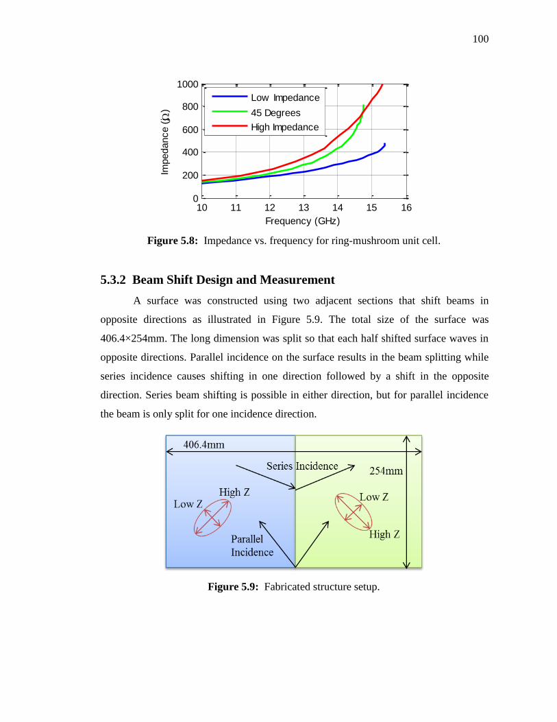
100
5.3.2 Beam Shift Design and Measurement
A surface was constructed using two adjacent sections that shift beams in
opposite directions as illustrated in Figure 5.9. The total size of the surface was
406.4×254mm. The long dimension was split so that each half shifted surface waves in
opposite directions. Parallel incidence on the surface results in the beam splitting while
series incidence causes shifting in one direction followed by a shift in the opposite
direction. Series beam shifting is possible in either direction, but for parallel incidence
the beam is only split for one incidence direction.
Figure 5.8: Impedance vs. frequency for ring-mushroom unit cell.
10 11 12 13 14 15 160
200
400
600
800
1000
Frequency (GHz)
Impedance (
j )
Low Impedance
45 Degrees
High Impedance
Figure 5.9: Fabricated structure setup.
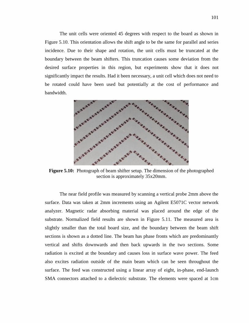
101
The unit cells were oriented 45 degrees with respect to the board as shown in
Figure 5.10. This orientation allows the shift angle to be the same for parallel and series
incidence. Due to their shape and rotation, the unit cells must be truncated at the
boundary between the beam shifters. This truncation causes some deviation from the
desired surface properties in this region, but experiments show that it does not
significantly impact the results. Had it been necessary, a unit cell which does not need to
be rotated could have been used but potentially at the cost of performance and
bandwidth.
The near field profile was measured by scanning a vertical probe 2mm above the
surface. Data was taken at 2mm increments using an Agilent E5071C vector network
analyzer. Magnetic radar absorbing material was placed around the edge of the
substrate. Normalized field results are shown in Figure 5.11. The measured area is
slightly smaller than the total board size, and the boundary between the beam shift
sections is shown as a dotted line. The beam has phase fronts which are predominantly
vertical and shifts downwards and then back upwards in the two sections. Some
radiation is excited at the boundary and causes loss in surface wave power. The feed
also excites radiation outside of the main beam which can be seen throughout the
surface. The feed was constructed using a linear array of eight, in-phase, end-launch
SMA connectors attached to a dielectric substrate. The elements were spaced at 1cm
Figure 5.10: Photograph of beam shifter setup. The dimension of the photographed
section is approximately 35x20mm.
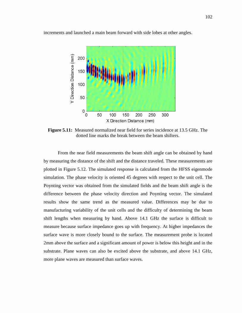
102
increments and launched a main beam forward with side lobes at other angles.
From the near field measurements the beam shift angle can be obtained by hand
by measuring the distance of the shift and the distance traveled. These measurements are
plotted in Figure 5.12. The simulated response is calculated from the HFSS eigenmode
simulation. The phase velocity is oriented 45 degrees with respect to the unit cell. The
Poynting vector was obtained from the simulated fields and the beam shift angle is the
difference between the phase velocity direction and Poynting vector. The simulated
results show the same trend as the measured value. Differences may be due to
manufacturing variability of the unit cells and the difficulty of determining the beam
shift lengths when measuring by hand. Above 14.1 GHz the surface is difficult to
measure because surface impedance goes up with frequency. At higher impedances the
surface wave is more closely bound to the surface. The measurement probe is located
2mm above the surface and a significant amount of power is below this height and in the
substrate. Plane waves can also be excited above the substrate, and above 14.1 GHz,
more plane waves are measured than surface waves.
Figure 5.11: Measured normalized near field for series incidence at 13.5 GHz. The
dotted line marks the break between the beam shifters.

103
The theory curve in Figure 5.12 uses the analysis performed in [66]. Zxx and Zyy
are taken from simulation (as plotted in Figure 5.8), and the orientation is set to 45°.
From these assumptions the shift angle can be solved and this angle is plotted in Figure
5.12. At low frequencies the theory closely matches the simulation but it deviates at
higher frequencies. At higher frequencies the spatial dispersion of the structure is
significant and the tensor impedance boundary condition no longer accurately models
the surface. This phenomenon has been discussed for a similar unit cell [26, 27]. In this
case, the surface exhibits larger beam shifts than the theory predicts. The approximate
theory is solved from (5.5) and significantly underestimates the beam shift angle across
the entire frequency range.
5.3.3 Surface Scattering
A surface scattering setup was used in parallel incidence. An H-plane sectoral
horn was placed at the boundary between the beam shifters. A metal cylinder (radius =
3.7cm) was placed on top of the surface and the surface profile was measured using the
same near field scanning setup. The results from the beam splitting setup are shown in
Figure 5.13. In Figure 5.14, a grounded 1.575mm thick slab of Rogers 5880 (εr = 2.2)
was measured with the same metal cylinder present. The area beneath the cylinder could
not be measured and is shown in black. The radius of the black region is 0.5cm larger
Figure 5.12: Beam shift angle results. The theory curve is solved from [66] and the
approximate theory is from (5.5).
11 11.5 12 12.5 13 13.5 14 14.50
10
20
30
40
Frequency (GHz)
Shift
Angle
(D
egre
es)
Measured
Simulation
Theory
Approximate
Theory

104
than the radius of the cylinder to ensure that the probe did not contact the cylinder. The
phase fronts exiting the horn were not completely straight but the horn was preferred
because it had less side lobes than the SMA splitter used for the series beam shift. In
Figure 5.13 the incident beam is split and minimal surface wave power is scattered by
the cylinder. Conversely, in Figure 5.14 the surface is isotropic and the beam directly
hits the cylinder and scatters in all directions. The wavelength is longer on the isotropic
surface because the structure has lower surface impedance. As discussed for the series
beam shift, the shift angle is frequency dependent. At 13.5 GHz, as shown in Figure
5.13, the incident beam mostly avoids the scattering object. However, at lower
frequencies the shift angle decreases (as plotted in Figure 5.12). As the shift angle
decreases the beams are directed more closely towards the scattering cylinder until the
limit where the shift angle is zero and a single beam travels directly at the cylinder as
shown in Figure 5.14.
Figure 5.13: Measured field results for beam splitting surface at 13.5 GHz.

105
5.5 Conclusion
A surface was created that reduces scattering from an object by sending incident
power in different directions. This type of structure could be used to shield regions on a
surface from surface waves incident externally, or to prevent interference between two
antennas on the same substrate. Similar patterning methods could be used for other
applications such as reducing the radar cross section of an object or guiding power in a
desired direction.
Chapter 5 is based on and mostly a reprint of the following papers: R. Quarfoth,
D. Sievenpiper, “Surface Wave Scattering Reduction Using Beam Shifters”, IEEE
Antennas and Wireless Propagation Letters, vol.13, pp. 963-966, 2014; R. Quarfoth, D.
Sievenpiper, “Anisotropic Surface Impedance Cloak”, IEEE Antennas and Propagation
Symposium Digest, Chicago, IL, USA, July 8-14, 2012.
Figure 5.14: Measured field results for isotropic impedance surface at 13.5 GHz.

106
Chapter 6 Manipulation of Scattering
Pattern Using Impedance Surfaces
6.1 Overview
Electromagnetic is relevant to multiple applications including imaging,
communications, radar, and antenna design. The scattering characteristics of an object
are predominantly determined by its shape and material. In this study, the scattering
profile of a shape is altered by patterning anisotropic impedance surfaces onto the
material. The scattered radiation from a rectangular object is altered as illustrated in
Figure 6.1. When a rectangular surface is illuminated by a plane wave normal to one
edge, it scatters the wave backwards towards the source. By patterning the object with
impedance surfaces, this backwards radiation can be changed to a different angle.
Various methods have been used to change the scattering pattern of an object.
Transformation electromagnetics allows precise control of propagation and scattering of
waves [58, 68]. Volumetric metamaterials were used to surround a cylindrical region
and cloak it [59, 69]. Transformation media have also been used to rotate
Figure 6.1: Scattering manipulation.

107
electromagnetic fields [62, 70, 71], and shift beams [60, 61], along with many other
applications. However, bulk metamaterials are generally electrically thick, narrow
bandwidth, heavy, and difficult to fabricate. Thin metasurfaces are advantageous
because they are light and easily fabricated. Surface impedance structures have been
used to reduce the scattering cross section of various shapes [11, 72]. These mantle
cloak structures work best on dielectrics (as opposed to metal), and cannot be easily
applied to electrically large metallic structures.
Impedance surfaces are an electromagnetic boundary condition that defines the
relationship between electric and magnetic fields within the surface. Electrically thin
surfaces can be modeled as impedance surfaces, and this allows electrically large
surfaces to be modeled efficiently. Impedance surfaces have been used to alter the
scattering of a coated metal cylinder [73], and further work has provided a method to
coat arbitrary three-dimensional shape with impedance surfaces [74]. Various numerical
and analytical techniques have also been studied for scattering from anisotropic
impedance surfaces [75-77]. Impedance surfaces have also been used for antennas [1, 7,
8], lenses [3, 78], transformation structures [66, 79], waveguides [14, 80], coatings for
horns [10], and for surface wave suppression [28].
In this investigation, a rectangular metallic object is coated with a lossless
anisotropic impedance surface, and the scattering is compared to an equivalent metal
rectangle. The impedance surfaces that are used are called hard and soft surfaces, which
have been analyzed previously [81, 82]. Hard surfaces support both transverse magnetic
(TM) and transverse electric (TE) surface modes, while soft surface support neither.
Hard and soft surfaces have been used in multiple ways to alter scattering properties
[83-85]. In this case, the hard and soft surfaces are used in a novel setup where a false
edge is created in the surface that scatters the incident wave as opposed to the real edges
of the metal rectangle. The surface is patterned in two sequential sections where the
incident region is a hard surface and the transmitted region is a soft surface. By
patterning an angled discontinuity between the two regions, the incident wave scatters at
an angle, and not back towards the source. This effect is achieved for both incident
polarizations.

108
6.2 Scattering Design
A side view of the scattering setup is shown in Figure 6.2. A finite rectangular
surface is located in the XY plane, and a plane wave is incident on the surface at an
angle θ. The rectangular surface is used because it has a simple scattering pattern with a
single main lobe in the backwards direction. The surface is assumed to have thickness
much less than the wavelength. The incident mode can have two polarizations, and any
other polarization is a superposition of the two. The TMi polarization has magnetic field
normal to the plane of incidence, and the TEi polarization has electric field normal to the
plane of incidence. In each case, the subscript labels the modes as related to the incident
wave.
For each incident polarization, a corresponding surface wave is excited with
similar field polarizations. However, these surface waves are distinct from the incident
plane wave, and they are also illustrated in Figure 6.2. Surface wave modes are excited
on the surface due to the incident radiation. On metals these are the standard surface
currents that exist in the presence of electromagnetic fields. On textured surfaces,
surface waves propagate bound to the surface [28]. TM surface wave modes have
magnetic field perpendicular to the direction of propagation, and TE modes have electric
field perpendicular to the direction of propagation. The orientation of the electric and
magnetic field components are the same in the respective surface wave modes and
incident plane waves. However, the relative magnitude and phase of each field
component are not the same. For surface modes the subscript is removed, and we will
subsequently refer to both the incident polarization and the corresponding surface mode
Figure 6.2: Mode polarizations of incident radiation and surface waves.
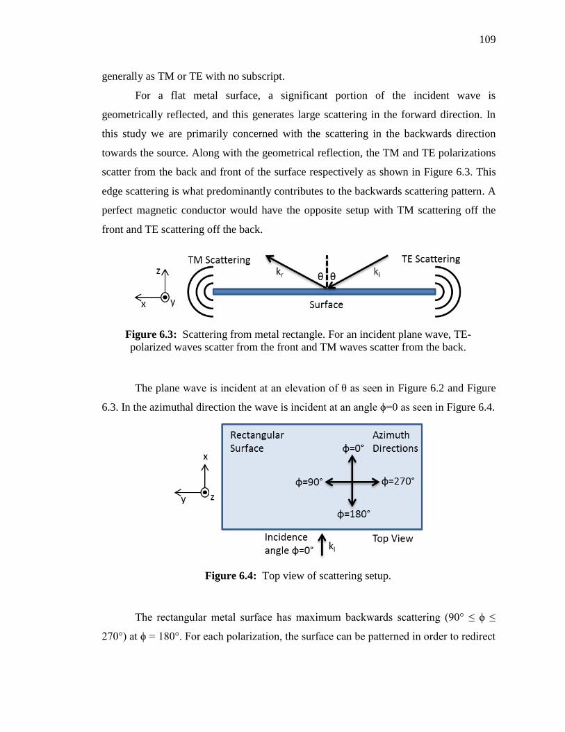
109
generally as TM or TE with no subscript.
For a flat metal surface, a significant portion of the incident wave is
geometrically reflected, and this generates large scattering in the forward direction. In
this study we are primarily concerned with the scattering in the backwards direction
towards the source. Along with the geometrical reflection, the TM and TE polarizations
scatter from the back and front of the surface respectively as shown in Figure 6.3. This
edge scattering is what predominantly contributes to the backwards scattering pattern. A
perfect magnetic conductor would have the opposite setup with TM scattering off the
front and TE scattering off the back.
The plane wave is incident at an elevation of θ as seen in Figure 6.2 and Figure
6.3. In the azimuthal direction the wave is incident at an angle ϕ=0 as seen in Figure 6.4.
The rectangular metal surface has maximum backwards scattering (90° ≤ ϕ ≤
270°) at ϕ = 180°. For each polarization, the surface can be patterned in order to redirect
Figure 6.3: Scattering from metal rectangle. For an incident plane wave, TE-
polarized waves scatter from the front and TM waves scatter from the back.
Figure 6.4: Top view of scattering setup.
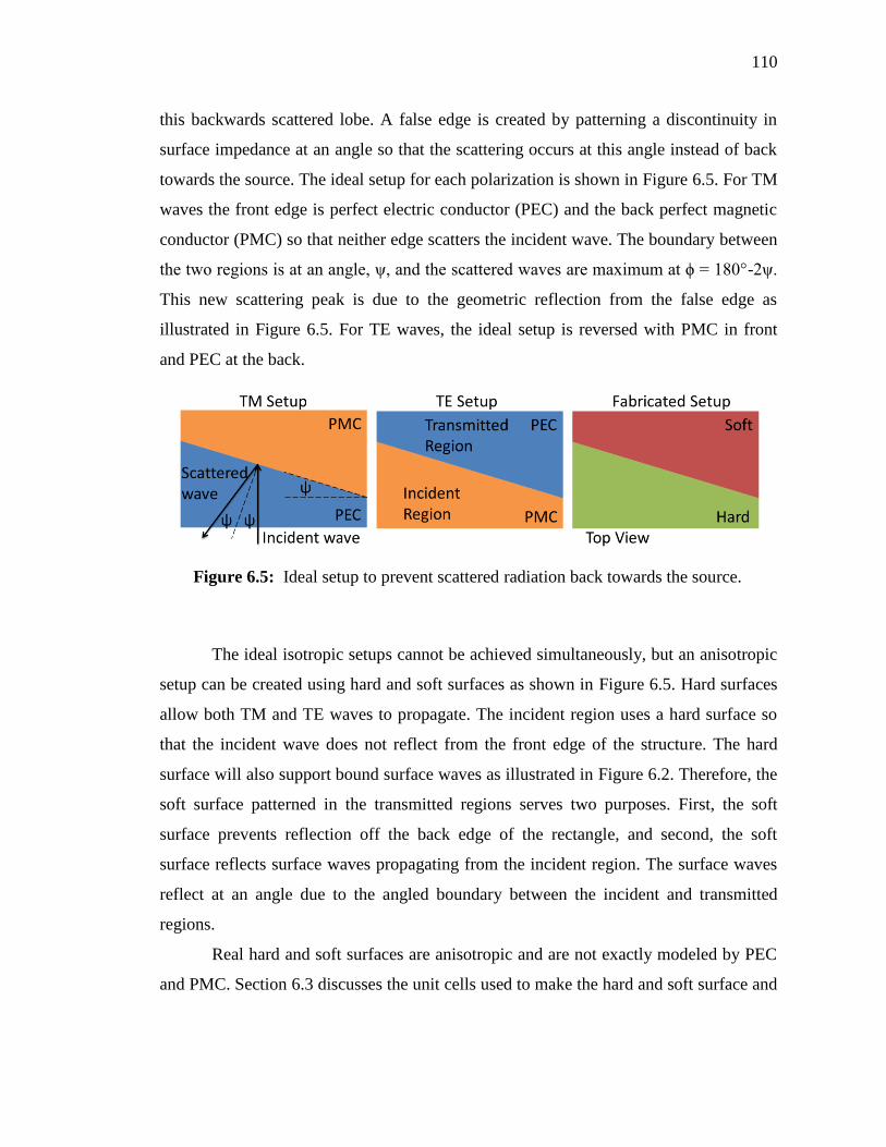
110
this backwards scattered lobe. A false edge is created by patterning a discontinuity in
surface impedance at an angle so that the scattering occurs at this angle instead of back
towards the source. The ideal setup for each polarization is shown in Figure 6.5. For TM
waves the front edge is perfect electric conductor (PEC) and the back perfect magnetic
conductor (PMC) so that neither edge scatters the incident wave. The boundary between
the two regions is at an angle, ψ, and the scattered waves are maximum at ϕ = 180°-2ψ.
This new scattering peak is due to the geometric reflection from the false edge as
illustrated in Figure 6.5. For TE waves, the ideal setup is reversed with PMC in front
and PEC at the back.
The ideal isotropic setups cannot be achieved simultaneously, but an anisotropic
setup can be created using hard and soft surfaces as shown in Figure 6.5. Hard surfaces
allow both TM and TE waves to propagate. The incident region uses a hard surface so
that the incident wave does not reflect from the front edge of the structure. The hard
surface will also support bound surface waves as illustrated in Figure 6.2. Therefore, the
soft surface patterned in the transmitted regions serves two purposes. First, the soft
surface prevents reflection off the back edge of the rectangle, and second, the soft
surface reflects surface waves propagating from the incident region. The surface waves
reflect at an angle due to the angled boundary between the incident and transmitted
regions.
Real hard and soft surfaces are anisotropic and are not exactly modeled by PEC
and PMC. Section 6.3 discusses the unit cells used to make the hard and soft surface and
Figure 6.5: Ideal setup to prevent scattered radiation back towards the source.

111
presents simulations showing the material properties of these materials. The ideal (using
PEC and PMC as illustrated in Figure 6.5) scattering structure was simulated using
Ansys HFSS version 15. The surface was 400mm wide and 200mm long, and the
boundary between PEC and PMC regions had angle of ψ = 21.8°. The surface was
excited by a near-grazing plane wave at an elevation of θ=70°. The backwards
directivity at θ=70° is plotted in Figure 6.6.
As expected, the PEC surface reflects each incident wave strongly back towards
the source at ϕ=180°. The patterned surfaces have relatively low scattering at ϕ=180°
(around ˗7dB). Instead, the largest scattering peak is located at 136 degrees, which 180°-
2ψ, as predicted by geometrical reflection. By changing the angle of the boundary
between PEC and PMC, the scattered lobe can be moved to other angles. The directivity
at ϕ=180° is reduced for each polarization by more than 10 dB.
6.3 Unit Cell Design and Simulation
In the idealized simulation of the structure, the PEC and PMC regions are both
isotropic. In a realized version this is not possible, and each region is instead created
with anisotropic impedance surfaces. Anisotropic impedance surfaces can be built by
Figure 6.6: Backward scattering of ideal setup.
100 120 140 160 180 200 220 240 260-30
-25
-20
-15
-10
-5
0
5
10
(deg)
Dir
ectivity T
ota
l (d
B)
TM patterned
TM PEC
TE Patterned
TE PEC

112
using periodic structures [7, 52]. The unit cell geometries are shown in Figure 6.7.
Dimensions of the cells are chosen for optimized results near 15 GHz. In each case, the
substrate is grounded Rogers 5880 with thickness 1.575mm. Each unit cell has an
identical copper patch that is rotated in the two cells. Periodic dipole patches on a
grounded dielectric have been used previously to create hard and soft surfaces [43, 86].
In this case the transmitted region unit cell has a plated metal via in order to suppress
surface wave propagation [28]. The plane wave is incident in the x-direction to the unit
cells, and for this orientation the incident and transmitted cells will be hard and soft
respectively. For waves incident in the y-direction, the incident and transmitted regions
switch to become soft and hard respectively. This is due to the anisotropy of the unit
cell.
The properties of the unit cells were simulated using HFSS. Normal incidence
reflection and surface wave propagation were both simulated in order to ensure that the
scattering characteristics are correct for incidence angles from normal to grazing. The
presence of the via does not have an effect on normal incidence reflection. The
simulated reflection phase of each unit cell is shown in Figure 6.8. The blue curve
shows the reflection for the electric field parallel to the long dimension of the patch.
This is the orientation for the incidence region under TE illumination and the
transmitted region under TM illumination.. At 15.4 GHz, the unit cell has a reflection
Figure 6.7: Top View of unit cell geometries. (a) shows the unit cell for the incident
region and (b) shows the unit cell for the transmitted region.

113
phase of 0 degrees which implies that it acts as PMC around this frequency range. The
range where the reflection phase is between -90 degrees and 90 degrees is from 12.4-
18.3 GHz. The red curve shows the reflection phase for electric field parallel to the short
dimension of the patch. This is the setup for the incidence region under TM illumination
and the transmitted region under TE illumination. At 15.4 GHz, the reflection phase is
111 degrees. From 12.4-18.3 GHz, the reflection phase varies from 128 degrees to 92
degrees. PEC has a phase delay of 180 degrees. The phase delay of the red curve would
be closer to 180 degrees if a thinner substrate was used, but at the cost of narrower
bandwidth (of the PMC reflection). Measurement results presented in Section 6.4 show
that these properties are sufficient to obtain good scattering results.
Surface wave propagation on each unit cell was simulated using the Eigenmode
solver of HFSS. The results for the incident region unit cell are shown in Figure 6.9. For
both TM and TE modes, the desired index value is one, and this represents PEC and
PMC respectively. When the index is one, reflection off the front edge is minimized for
both polarizations. As the index deviates from one, reflection increases. The effective
Figure 6.8: Reflection phase of unit cells. In the blue curve the electric field is
parallel to the long patch dimension. The red curve has electric field parallel to the
short dimension of the patch.
10 11 12 13 14 15 16 17 18 19 20-150
-100
-50
0
50
100
150
Frequency (GHz)
Phase (
deg)
E // Long
E // Short

114
surface index can be directly related to the surface impedance [7]. The simulated TM
mode has low index over a broad bandwidth. The TE mode has a cutoff at 15.2 GHz.
Bound surface wave moves are not supported below this frequency, and the surface
impedance is not defined. However, leaky modes are supported below cutoff, and modes
in this region have effective index below one. The TE mode has an index of one at
cutoff, and the index quickly rises with frequency.
The dispersion characteristics of the transmitted-region unit cell are shown in
Figure 6.10. The dispersion of both TM and TE modes are shown along with the
dispersion of light in a vacuum. Bound surface waves only exist below the light line. A
surface wave bandgap exists between the top of the TM mode at 11.8 GHz and the
cutoff of the TE mode at 23 GHz. Surface propagation cannot occur within the bandgap,
so surface waves from the incident region will be reflected from the transmitted region
for both TM and TE modes. Since the boundary is angled, these reflected surface waves
will not scatter back towards the source. Along with surface wave scattering, the
incident plane wave scatters directly from discontinuity between the incident and
transmitted regions.
Figure 6.9: Surface index of TM and TE surface waves on incident region.
10 11 12 13 14 15 16 17 18 19 201
1.1
1.2
1.3
1.4
1.5
Frequency (GHz)
Index
TM Mode
TE Mode

115
6.4 Scattering Measurement
A surface was fabricated using the design discussed in Section 6.2 and the unit
cells discussed in Section 6.3. The surface was 400×200mm (100×50 unit cells), and the
angled discontinuity was at ψ = 21.8°. Unit cells were patterned above and below a
ground plane, and the substrate was Rogers 5880 with a thickness of 1.575mm (making
a total surface thickness of 3.15mm). Simulation showed that for TM incidence only the
top surface of the rectangle needed to be patterned. However, for TE incidence, the
surface needed to be patterned on both top and bottom in order to maximally reduce the
backwards scattering. A photograph of the fabricated surface is shown in Figure 6.11.
Figure 6.10: Unit cell dispersion of transmitted section.
100 200 300 400 500 600 7005
10
15
20
25
30
k (m-1)
Fre
quency (
GH
z)
TM Mode
TE Mode
Light

116
The structure was measured under TM and TE illumination. Two KU band
pyramidal horns were used as sources and S21 between the horns was measured using
an Agilent E5071C VNA. The operating band of each horn was 12.4-18 GHz with a
TE10 cutoff at 9.5 GHz and a TE20 cutoff at 19.0 GHz. The measurement was performed
in an anechoic chamber. Microwave absorbing foam was placed between the two horns
in order to prevent direct coupling as seen in Figure 6.12. Without this foam, significant
(a)
(b)
Figure 6.11: Fabricated patterned rectangular surface. (a) shows a full view of the
surface and (b) shows a zoomed-in version.

117
coupling occurred for the TE polarization. Each horn was placed at an incident angle of
θ = 70° and ϕ = 180°. The surface was mounted on a pedestal which rotated with respect
to the horns. At each rotation, the scattering transmission was measured. Note that this is
a different setup from the results in Figure 6.6 where the directivity of scattered
radiation was simulated using a fixed source and sample.
The measured TM and TE scattering at 15 GHz is shown in Figure 6.13. For
each polarization, the patterned surface is compared to a metal surface of the same
dimensions, and S21 is plotted with respect to the angle of the surface. At an angle of
180°, the incident wave is normal to the surface. At this angle, the metal has large
scattering for both TM and TE illumination. At all other angles the metal has low
scattering (note that at angles 90° and 270° the wave is incident normally to the short
side of the rectangle). For the patterned surface, both TM and TE scattering is reduced
by more than 10 dB at 180°. This was the goal of the design. A new scattering peak is
located at 158° due to the angled boundary, where 158° = 180°-ψ. In Figure 6.6 the plot
is of the directivity of the scattered radiation, so the peak is at 180°-2ψ.
Figure 6.12: Measurement Setup. A second identical horn antenna is located on the
far side of the foam barrier. The absorbing foam is used to reduce coupling between
the horns.

118
(a)
(b)
Figure 6.13: Measured scattering transmission vs. rotation angle of the surface. (a)
shows the scattering for TM incidence and (b) shows the scattering for TE incidence.
Only backwards scattering is shown.

119
For TM incidence, surface waves are supported in many directions along the
surface and extra scattering peaks are generated due to reflections within the surface.
For TE incidence, surface waves are only supported in the forward direction and only a
single scattered peak is generated. The magnitude of the TE scattered peak is relatively
lower because power is launched more strongly at other elevation angles. Measurements
at a near-grazing elevation angle of θ = 80° were also performed (these results are not
shown). The results were similar to the θ = 70° except the metal sheet has minimal
reflection for TM incidence. This is because at grazing incidence, a metal sheet will not
reflect the TM polarization at any elevation.
The transmission-reduction between the patterned and metal surfaces is shown in
Figure 6.14. The vertical-axis shows the difference in S21 between the patterned surface
and the metal surface in the normal-incidence orientation (θ = 70° and ϕ = 180°). The
peak reduction in scattering is around 15 GHz where reflection phase is near 180° for
the PMC regions (as seen in Figure 6.8), and where the index equals one for the TE
mode in the incident region (as seen in Figure 6.9). Above 19 GHz both TM and TE
polarizations show increased scattering as compared to the metal surface. At 10 GHz,
the reduction in TE scattering is approaching zero, while the TM mode still shows a
reduction in scattering of nearly 10dB. However, as seen in Figure 6.13, a small
scattered peak exists at 189° for TM illumination. At 15 GHz, this peak is more than 10
dB below the metal peak, but from 12 to 10 GHz, the peak rises to the same height as
the metal peak. Accounting for this second scattering peak, the bandwidth of patterned
surface is similar for TM and TE illumination. For each polarization, backwards
scattering is reduced over multiple GHz around the design frequency of 15 GHz.

120
6.5 Conclusion
A rectangular surface was patterned with anisotropic impedance surfaces in
order to alter the backwards scattering as compared to a metal conductor. The effect was
achieved by placing an angled boundary in the patterned surface that reflects incident
waves in a different direction. The structure has two different regions on either side of
the boundary. The incidence region was a hard surface and the transmitted region was a
soft surface. Using reconfigurable or tunable structures, the surface could be
electronically adjusted to reflect to different angles. Similarly, the frequency where the
peak reduction occurs could be electronically controlled. This type of structure would
allow a designer to set the scattering characteristics of the object based on the
environment and adjust the characteristics dynamically.
Figure 6.14: Measured reduction in backwards scattering. The scattering is the
difference between the patterned surface and the metal surface.
10 12 14 16 18 20-15
-10
-5
0
5
10
Frequency (GHz)
Patt
ern
ed C
om
pare
d t
o M
eta
l S
urf
ace (
dB
)
TM
TE

121
Chapter 7 Conclusion
7.1 Summary of Work
This thesis presents an investigation into the theory and applications of
anisotropic artificial impedance surfaces.
Chapter 2 reviews the fundamental properties of anisotropic impedance surfaces.
The surfaces are modeled as a 2×2 boundary condition which relates the electric and
magnetic fields on the surface. Periodic unit cells can be used to physically realize the
surfaces, and the HFSS eigenmode simulator is used to analyze the properties. An
example of rectangular and diamond unit cells are presented which show how the unit
cell can be patterned to achieve a desired anisotropic tensor impedance.
Chapter 3 presents an in depth analysis of unit cell geometries. Multiple different
designs are tested in order to observe the limitations of bandwidth and anistropy. A ring-
mushroom unit cell gives the best performance. More generally it is shown that larger
thickness and higher permittivity lead to improved performance. It is also discussed that
anisotropic impedance surface must be used at frequencies where only a single mode is
supported. Otherwise, modes interfere and give erroneous results.
Chapter 4 analyzes anisotropic surface impedance waveguides. It is shown that
the surface can be patterned such that a confined waveguide mode is supported and
propagates bound within this region. The dispersion relation of surface wave
waveguides is analyzed using a ray optics method and shown to match simulation and a
fabricated structure. Analysis and measurements of a curved structure and bending
losses is also performed.
Chapter 5 presents a surface wave beam splitter which can reduce the surface
wave scattering from an object on the surface. The beam splitter is created from two
adjacent beam shifters. A cloaking structure is also shown in simulation that splits apart

122
the surface wave and the recombines it in phase on the far side of a cloaked region.
Chapter 6 presents a surface patterning technique that has the ability to alter the
scattering properties of an object. By patterning a rectangular surface with an artificial
angled boundary, the backwards scattering from the surface can be significantly
reduced.
7.2 Future Work
Current impedance surface applications generally use square, rectangular, or
hexagonal unit cells because they are most easily patterned together to make large
shapes. However, limiting a design to a single unit cell size can significantly reduce the
range of obtainable surface impedances. By patterning with continuously varying unit
cell dimensions, it may be possible to more accurately achieve a desired impedance
profile across a surface. This would more easily allow structures where the impedance
varies gradually and continuously across the surface. In these cases, the unit cell sizes
and geometries could be changed with position in order to improve the pattern. In order
to perform this patterning technique, algorithms are being developed that automatically
pattern unit cells based on the impedance surface.
In this thesis, each design was static and operated in a single state. For practical
implementations, impedance surfaces can be made reconfigurable or tunable by using
switches, varactors, tunable materials, or other methods. This would allow each design
to operate over different frequency bands or in different settings. For instance, the
impedance surface waveguides could be switched to connect different elements on a
surface at a different time. In the same way, the beam shifter could be tuned to different
frequencies depending on the source of incoming radiation. For the radar scattering
surface, the angle of scattered radiation could be changed if the surface is rotated or if
the source changes position. However, in any case, the cost and design challenges of an
active surface are generally increased as compared to the static and passive surface
presented in this thesis.

123
Bibliography
[1] A. M. Patel and A. Grbic, "A Printed Leaky-Wave Antenna Based on a
Sinusoidally-Modulated Reactance Surface," Antennas and Propagation, IEEE
Transactions on, vol. 59, pp. 2087-2096, 2011.
[2] G. Minatti, F. Caminita, M. Casaletti, and S. Maci, "Spiral Leaky-Wave
Antennas Based on Modulated Surface Impedance," Antennas and Propagation,
IEEE Transactions on, vol. 59, pp. 4436-4444, 2011.
[3] M. Bosiljevac, M. Casaletti, F. Caminita, Z. Sipus, and S. Maci, "Non-Uniform
Metasurface Luneburg Lens Antenna Design," Antennas and Propagation, IEEE
Transactions on, vol. 60, pp. 4065-4073, 2012.
[4] A. Dhouibi, S. N. Burokur, A. de Lustrac, and A. Priou, "Compact
Metamaterial-Based Substrate-Integrated Luneburg Lens Antenna," Antennas
and Wireless Propagation Letters, IEEE, vol. 11, pp. 1504-1507, 2012.
[5] D. Gregoire and A. Kabakian, "Surface-Wave Waveguides," Antennas and
Wireless Propagation Letters, IEEE, vol. PP, pp. 1-1, 2011.
[6] H. J. Bilow, "Guided waves on a planar tensor impedance surface," Antennas
and Propagation, IEEE Transactions on, vol. 51, pp. 2788-2792, 2003.
[7] B. H. Fong, J. S. Colburn, J. J. Ottusch, J. L. Visher, and D. F. Sievenpiper,
"Scalar and Tensor Holographic Artificial Impedance Surfaces," Antennas and
Propagation, IEEE Transactions on, vol. 58, pp. 3212-3221, 2010.
[8] G. Minatti, S. Maci, P. De Vita, A. Freni, and M. Sabbadini, "A Circularly-
Polarized Isoflux Antenna Based on Anisotropic Metasurface," Antennas and
Propagation, IEEE Transactions on, vol. 60, pp. 4998-5009, 2012.
[9] W. Qi, C. P. Scarborough, D. H. Werner, E. Lier, and X. Wang, "Design
Synthesis of Metasurfaces for Broadband Hybrid-Mode Horn Antennas With
Enhanced Radiation Pattern and Polarization Characteristics," Antennas and
Propagation, IEEE Transactions on, vol. 60, pp. 3594-3604, 2012.
[10] W. Qi, C. P. Scarborough, B. G. Martin, R. K. Shaw, D. H. Werner, E. Lier, and

124
X. Wang, "A Ku-Band Dual Polarization Hybrid-Mode Horn Antenna Enabled
by Printed-Circuit-Board Metasurfaces," Antennas and Propagation, IEEE
Transactions on, vol. 61, pp. 1089-1098, 2013.
[11] P.-Y. Chen and A. Alù, "Mantle cloaking using thin patterned metasurfaces,"
Physical Review B, vol. 84, p. 205110, 11/10/ 2011.
[12] A. Monti, J. Soric, A. Alu, F. Bilotti, A. Toscano, and L. Vegni, "Overcoming
Mutual Blockage Between Neighboring Dipole Antennas Using a Low-Profile
Patterned Metasurface," Antennas and Wireless Propagation Letters, IEEE, vol.
11, pp. 1414-1417, 2012.
[13] A. Monti, F. Bilotti, A. Toscano, J. Soric, and A. Alu, "Mantle cloak devices for
TE and TM polarizations," in Antennas and Propagation Society International
Symposium (APSURSI), 2013 IEEE, 2013, pp. 324-325.
[14] R. Quarfoth and D. Sievenpiper, "Artificial Tensor Impedance Surface
Waveguides," Antennas and Propagation, IEEE Transactions on, vol. 61, pp.
3597-3606, 2013.
[15] R. Quarfoth and D. Sievenpiper, "Anisotropic surface impedance cloak," in
Antennas and Propagation Society International Symposium (APSURSI), 2012
IEEE, 2012, pp. 1-2.
[16] C. L. Holloway, E. F. Kuester, J. A. Gordon, J. O'Hara, J. Booth, and D. R.
Smith, "An Overview of the Theory and Applications of Metasurfaces: The
Two-Dimensional Equivalents of Metamaterials," Antennas and Propagation
Magazine, IEEE, vol. 54, pp. 10-35, 2012.
[17] S. Ramo, J. R. Whinnery, and T. V. Duzer, Fields and Waves in Communication
Electronics, Second ed. New York: John Wiley & Sons, 1984, ch 9.
[18] S. W. Lee and W. R. Jones, "Surface Waves on Two-Dimensional Corrugated
Structures," Radio Science, vol. 6, pp. 811-818, 1971.
[19] W. Rotman, "A Study of Single-Surface Corrugated Guides," Proceedings of the
IRE, vol. 39, pp. 952-959, 1951.
[20] R. King, D. Thiel, and K. Park, "The synthesis of surface reactance using an
artificial dielectric," Antennas and Propagation, IEEE Transactions on, vol. 31,
pp. 471-476, 1983.
[21] M. G. Silveirinha, C. A. Fernandes, and J. R. Costa, "Electromagnetic
Characterization of Textured Surfaces Formed by Metallic Pins," Antennas and
Propagation, IEEE Transactions on, vol. 56, pp. 405-415, 2008.

125
[22] W. L. Barnes, S. C. Kitson, T. W. Preist, and J. R. Sambles, "Photonic surfaces
for surface-plasmon polaritons," J. Opt. Soc. Am. A, vol. 14, pp. 1654-1661,
1997.
[23] Y. Liu, T. Zentgraf, G. Bartal, and X. Zhang, "Transformational Plasmon
Optics," Nano Letters, vol. 10, pp. 1991-1997, 2010/06/09 2010.
[24] T. Zentgraf, Y. Liu, M. H. Mikkelsen, J. Valentine, and X. Zhang, "Plasmonic
Luneburg and Eaton lenses," Nat Nano, vol. 6, pp. 151-155, 2011.
[25] S. Tricarico, F. Bilotti, A. Alù, and L. Vegni, "Plasmonic cloaking for irregular
objects with anisotropic scattering properties," Physical Review E, vol. 81, p.
026602, 02/18/ 2010.
[26] A. M. Patel and A. Grbic, "Modeling and Analysis of Printed-Circuit Tensor
Impedance Surfaces," Antennas and Propagation, IEEE Transactions on, vol.
61, pp. 211-220, 2013.
[27] A. M. Patel and A. Grbic, "Effective Surface Impedance of a Printed-Circuit
Tensor Impedance Surface (PCTIS)," Microwave Theory and Techniques, IEEE
Transactions on, vol. 61, pp. 1403-1413, 2013.
[28] D. Sievenpiper, Z. Lijun, R. F. J. Broas, N. G. Alexopolous, and E.
Yablonovitch, "High-impedance electromagnetic surfaces with a forbidden
frequency band," Microwave Theory and Techniques, IEEE Transactions on,
vol. 47, pp. 2059-2074, 1999.
[29] D. F. Sievenpiper, J. H. Schaffner, H. J. Song, R. Y. Loo, and G. Tangonan,
"Two-dimensional beam steering using an electrically tunable impedance
surface," Antennas and Propagation, IEEE Transactions on, vol. 51, pp. 2713-
2722, 2003.
[30] C. Mias and Y. Jyh Haur, "A Varactor-Tunable High Impedance Surface With a
Resistive-Lumped-Element Biasing Grid," Antennas and Propagation, IEEE
Transactions on, vol. 55, pp. 1955-1962, 2007.
[31] C. S. R. Kaipa, A. B. Yakovlev, S. I. Maslovski, and M. G. Silveirinha,
"Mushroom-Type High-Impedance Surface With Loaded Vias: Homogenization
Model and Ultra-Thin Design," Antennas and Wireless Propagation Letters,
IEEE, vol. 10, pp. 1503-1506, 2011.
[32] D. J. Hoppe and Y. Rahmat-Samii, Impedance boundary conditions in
electromagnetics. Washington, DC: Taylor & Francis, 1995.
[33] R. Quarfoth and D. Sievenpiper, "Simulation of anisotropic artificial impedance
surface with rectangular and diamond lattices," in Antennas and Propagation

126
(APSURSI), 2011 IEEE International Symposium on, 2011, pp. 1498-1501.
[34] R. A. Shelby, D. R. Smith, and S. Schultz, "Experimental Verification of a
Negative Index of Refraction," Science, vol. 292, pp. 77-79, 2001.
[35] C. G. Parazzoli, R. B. Greegor, K. Li, B. E. C. Koltenbah, and M. Tanielian,
"Experimental Verification and Simulation of Negative Index of Refraction
Using Snell’s Law," Physical Review Letters, vol. 90, p. 107401, 03/11/ 2003.
[36] G. V. Eleftheriades, A. K. Iyer, and P. C. Kremer, "Planar negative refractive
index media using periodically L-C loaded transmission lines," Microwave
Theory and Techniques, IEEE Transactions on, vol. 50, pp. 2702-2712, 2002.
[37] A. Grbic and G. V. Eleftheriades, "Experimental verification of backward-wave
radiation from a negative refractive index metamaterial," Journal of Applied
Physics, vol. 92, pp. 5930-5935, 2002.
[38] C. Caloz, A. Sanada, and T. Itoh, "A novel composite right-/left-handed
coupled-line directional coupler with arbitrary coupling level and broad
bandwidth," Microwave Theory and Techniques, IEEE Transactions on, vol. 52,
pp. 980-992, 2004.
[39] T. Tamir and K. Foon, "Varieties of leaky waves and their excitation along
multilayered structures," Quantum Electronics, IEEE Journal of, vol. 22, pp.
544-551, 1986.
[40] A. B. Yakovlev and G. W. Hanson, "Leaky-wave dispersion behavior on a
grounded ferrite slab waveguide," Microwave and Wireless Components Letters,
IEEE, vol. 12, pp. 398-400, 2002.
[41] D. F. Sievenpiper, "Forward and backward leaky wave radiation with large
effective aperture from an electronically tunable textured surface," Antennas and
Propagation, IEEE Transactions on, vol. 53, pp. 236-247, 2005.
[42] A. B. Yakovlev, M. G. Silveirinha, O. Luukkonen, C. R. Simovski, I. S.
Nefedov, and S. A. Tretyakov, "Characterization of Surface-Wave and Leaky-
Wave Propagation on Wire-Medium Slabs and Mushroom Structures Based on
Local and Nonlocal Homogenization Models," Microwave Theory and
Techniques, IEEE Transactions on, vol. 57, pp. 2700-2714, 2009.
[43] S. Maci, M. Caiazzo, A. Cucini, and M. Casaletti, "A pole-zero matching
method for EBG surfaces composed of a dipole FSS printed on a grounded
dielectric slab," Antennas and Propagation, IEEE Transactions on, vol. 53, pp.
70-81, 2005.
[44] A. M. Patel and A. Grbic, "The Effects of Spatial Dispersion on Power Flow

127
Along a Printed-Circuit Tensor Impedance Surface," Antennas and Propagation,
IEEE Transactions on, vol. 62, pp. 1464-1469, 2014.
[45] M. C. Simon, "Ray tracing formulas for monoaxial optical components," Appl.
Opt., vol. 22, pp. 354-360, 1983.
[46] Q.-T. Liang, "Simple ray tracing formulas for uniaxial optical crystals," Appl.
Opt., vol. 29, pp. 1008-1010, 1990.
[47] W.-Q. Zhang, "General ray-tracing formulas for crystal," Appl. Opt., vol. 31, pp.
7328-7331, 1992.
[48] M. Sluijter, "Ray-optics analysis of inhomogenous optically anisotropic media,"
Ph.D., TNW Optics Research Group, Delft University of Technology,
Koninklijke Philips Electronics N.V., 2010.
[49] B. E. A. Saleh and M. C. Teich, Fundamentals of photonics. New York: Wiley,
1991.
[50] Y. Satomura, M. Matsuhara, and N. Kumagai, "Analysis of Electromagnetic-
Wave Modes in Anisotropic Slab Waveguide," Microwave Theory and
Techniques, IEEE Transactions on, vol. 22, pp. 86-92, 1974.
[51] S. R. Seshadri, "Ray model for a planar anisotropic dielectric waveguide," J.
Opt. Soc. Am. A, vol. 15, pp. 972-977, 1998.
[52] R. Quarfoth and D. Sievenpiper, "Broadband Unit Cell Design for Highly-
Anisotropic Impedance Surfaces," Antennas and Propagation, IEEE
Transactions on, vol. PP, pp. 1-1, 2014.
[53] E. A. J. Marcatili, "Bends in Optical Dielectric Guides," Bell System Technical
Journal, vol. 48, pp. 2103-2132, 1969.
[54] A. W. Snyder, "Generalised Fresnel's law for loss due to curvature," Electronics
Letters, vol. 9, pp. 609-610, 1973.
[55] A. W. Snyder and D. J. Mitchell, "Bending losses of multimode optical fibres,"
Electronics Letters, vol. 10, pp. 11-12, 1974.
[56] A. W. Snyder and J. Love, Optical waveguide theory vol. 190: Springer, 1983.
[57] M. Remouche, R. Mokdad, A. Chakari, and P. Meyrueis, "Intrinsic integrated
optical temperature sensor based on waveguide bend loss," Optics & Laser
Technology, vol. 39, pp. 1454-1460, 10// 2007.
[58] J. B. Pendry, D. Schurig, and D. R. Smith, "Controlling Electromagnetic Fields,"

128
Science, vol. 312, pp. 1780-1782, 2006.
[59] D. Schurig, J. J. Mock, B. J. Justice, S. A. Cummer, J. B. Pendry, A. F. Starr,
and D. R. Smith, "Metamaterial Electromagnetic Cloak at Microwave
Frequencies," Science, vol. 314, pp. 977-980, 2006.
[60] M. Rahm, S. A. Cummer, D. Schurig, J. B. Pendry, and D. R. Smith, "Optical
Design of Reflectionless Complex Media by Finite Embedded Coordinate
Transformations," Physical Review Letters, vol. 100, p. 063903, 2008.
[61] P. A. Huidobro, M. L. Nesterov, L. Mart n-Moreno, and F. . arc a-Vidal,
"Transformation Optics for Plasmonics," Nano Letters, vol. 10, pp. 1985-1990,
2010/06/09 2010.
[62] H. Chen and C. T. Chan, "Electromagnetic wave manipulation by layered
systems using the transformation media concept," Physical Review B, vol. 78, p.
054204, 2008.
[63] G. Gok and A. Grbic, "A Printed Beam-Shifting Slab Designed Using Tensor
Transmission-Line Metamaterials," Antennas and Propagation, IEEE
Transactions on, vol. 61, pp. 728-734, 2013.
[64] O. Siddiqui and G. V. Eleftheriades, "Resonance-cone focusing in a
compensating bilayer of continuous hyperbolic microstrip grids," Applied
Physics Letters, vol. 85, pp. 1292-1294, 2004.
[65] M. Selvanayagam and G. V. Eleftheriades, "Experimental Verification of the
Effective Medium Properties of a Transmission-Line Metamaterial on a Skewed
Lattice," Antennas and Wireless Propagation Letters, IEEE, vol. 10, pp. 1495-
1498, 2011.
[66] A. M. Patel and A. Grbic, "Transformation Electromagnetics Devices Based on
Printed-Circuit Tensor Impedance Surfaces," Microwave Theory and
Techniques, IEEE Transactions on, vol. 62, pp. 1102-1111, 2014.
[67] R. Quarfoth and D. Sievenpiper, "Unit Cell for Highly-Anisotropic Tensor
Impedance Surface," Transactions on Antennas and Propagation, vol. Accepted
for Publication, 2014.
[68] U. Leonhardt, "Optical Conformal Mapping," Science, vol. 312, pp. 1777-1780,
2006.
[69] B. Kanté, D. Germain, and A. de Lustrac, "Experimental demonstration of a
nonmagnetic metamaterial cloak at microwave frequencies," Physical Review B,
vol. 80, p. 201104, 11/17/ 2009.

129
[70] H. Chen and C. T. Chan, "Transformation media that rotate electromagnetic
fields," Applied Physics Letters, vol. 90, pp. -, 2007.
[71] J. Hao, Y. Yuan, L. Ran, T. Jiang, J. A. Kong, C. T. Chan, and L. Zhou,
"Manipulating Electromagnetic Wave Polarizations by Anisotropic
Metamaterials," Physical Review Letters, vol. 99, p. 063908, 08/10/ 2007.
[72] J. C. Soric, P. Y. Chen, A. Kerkhoff, D. Rainwater, K. Melin, and A. Alù,
"Demonstration of an ultralow profile cloak for scattering suppression of a
finite-length rod in free space," New Journal of Physics, vol. 15, p. 033037,
2013.
[73] J. S. Colburn, D. F. Sievenpiper, B. H. Fong, J. J. Ottusch, J. L. Visher, and P. R.
Herz, "Advances in Artificial Impedance Surface Conformal Antennas," in
Antennas and Propagation Society International Symposium, 2007 IEEE, 2007,
pp. 3820-3823.
[74] D. J. Gregoire, "3-D Conformal Metasurfaces," Antennas and Wireless
Propagation Letters, IEEE, vol. 12, pp. 233-236, 2013.
[75] G. Pelosi, G. Manara, and P. Nepa, "A UTD solution for the scattering by a
wedge with anisotropic impedance faces: skew incidence case," Antennas and
Propagation, IEEE Transactions on, vol. 46, pp. 579-588, 1998.
[76] G. Pelosi, G. Manara, and M. Fallai, "Physical optics expressions for the fields
scattered from anisotropic impedance flat plates," Microwave and Optical
Technology Letters, vol. 14, pp. 316-318, 1997.
[77] H. J. Bilow, "Scattering by an infinite wedge with tensor impedance boundary
conditions-a moment method/physical optics solution for the currents," Antennas
and Propagation, IEEE Transactions on, vol. 39, pp. 767-773, 1991.
[78] H. Ming, Y. Shiwen, G. Fei, R. Quarfoth, and D. Sievenpiper, "A 2-D
Multibeam Half Maxwell Fish-Eye Lens Antenna Using High Impedance
Surfaces," Antennas and Wireless Propagation Letters, IEEE, vol. 13, pp. 365-
368, 2014.
[79] R. Quarfoth and D. Sievenpiper, "Surface Wave Scattering Reduction Using
Beam Shifters," Antennas and Wireless Propagation Letters, IEEE, vol. 13, pp.
963-966, 2014.
[80] D. Gregoire and A. Kabakian, "Surface-Wave Waveguides," Antennas and
Wireless Propagation Letters, IEEE, vol. 10, pp. 1512-1515, 2011.
[81] P. S. Kildal, "Definition of artificially soft and hard surfaces for electromagnetic
waves," Electronics Letters, vol. 24, pp. 168-170, 1988.

130
[82] P. S. Kildal, "Artificially soft and hard surfaces in electromagnetics," Antennas
and Propagation, IEEE Transactions on, vol. 38, pp. 1537-1544, 1990.
[83] P. S. Kildal, A. A. Kishk, and A. Tengs, "Reduction of forward scattering from
cylindrical objects using hard surfaces," Antennas and Propagation, IEEE
Transactions on, vol. 44, pp. 1509-1520, 1996.
[84] G. Manara, P. Nepa, and G. Pelosi, "High-frequency EM scattering by edges in
artificially hard and soft surfaces illuminated at oblique incidence," Antennas
and Propagation, IEEE Transactions on, vol. 48, pp. 790-800, 2000.
[85] M. Paquay, J. C. Iriarte, I. Ederra, R. Gonzalo, and P. de Maagt, "Thin AMC
Structure for Radar Cross-Section Reduction," Antennas and Propagation, IEEE
Transactions on, vol. 55, pp. 3630-3638, 2007.
[86] S. Maci and P. S. Kildal, "Hard and soft surfaces realized by FSS printed on a
grounded dielectric slab," in Antennas and Propagation Society International
Symposium, 2004. IEEE, 2004, pp. 285-288 Vol.1.