university of alberta · acknowledgements at rst, i would like to express my deep thanks to my...
TRANSCRIPT

University of Alberta
REAL-TIME HARDWARE EMULATION OF A MULTIFUNCTIONPROTECTION SYSTEM
by
Yifan Wang
A thesis submitted to the Faculty of Graduate Studies and Researchin partial fulfillment of the requirements for the degree of
Master of Science
in
Energy Systems
Department of Electrical and Computer Engineering
c© Yifan WangSpring 2014
Edmonton, Alberta
Permission is hereby granted to the University of Alberta Libraries to reproduce single copies of this thesisand to lend or sell such copies for private, scholarly or scientific research purposes only. Where the thesis is
converted to, or otherwise made available in digital form, the University of Alberta will advise potentialusers of the thesis of these terms.
The author reserves all other publication and other rights in association with the copyright in the thesis and,except as herein before provided, neither the thesis nor any substantial portion thereof may be printed or
otherwise reproduced in any material form whatsoever without the authors prior written permission.

To my parents, Xiaorong Li and Guopei Wang, for their love, support, and
always being there for me.

Abstract
The need for high-speed multifunction protective relays in modern power
systems is growing. A relay’s fast response and reliable operation to clear
faults is essential, especially in the context of smart grids. This research pro-
poses a low-latency hardware digital multifunction protective relay on the Field
Programmable Gate Array (FPGA). Taking advantage of inherent hard-wired
architecture of the FPGA, the proposed hardware relay design is paralleled
and fully pipelined to achieve low latencies in various relay modules which are
developed in hardware description language. This low-latency feature allows
fast operation and data throughput to reach higher computational efficiency.
In addition, the parallelism and the hardwired architecture of the FPGA make
the design more reliable in computation than the sequential software-based nu-
meric relay. The case studies demonstrate the effectiveness of the multifunction
hardware relay.

Acknowledgements
At first, I would like to express my deep thanks to my supervisor, Dr.
Venkata Dinavahi for his support and supervision in various aspects of my
research. Without his continuous encouragement, motivation and advice on
my research, the work presented in the thesis could not have been finished.
Furthermore, I learned from Dr. Dinavahi his positive thinking and enthusiasm
for both work and life. Those cheering and valuable words and instructions will
be cherished forever.
I also would like to thank Dr. Behrouz Nowrouzian and Dr. Jie Han
gratefully for taking their time to serve my examination committee. Dr. Han
was also my ASIC design course instructor and offered great lectures that are
useful in my research work.
Thanks to all my colleagues and friends in RTX-Lab, Pengfei, Gene, Jiadai,
Yuan, Wentao, You, Hadis, Nariman, especially Pengfei who helped me a lot
on the DAC implementation and gave me valuable suggestions. Also thanks
to all my other friends within and outside the ECE department who are not
listed here, for their warm friendship, accompanying, listening and hints for
life and study. Special thanks to my former colleagues, James and Guy, for
their guidance and valuable suggestions on power system protection engineering
during my internship. And sincere thanks to my friend Jack who gave me
many valuable suggestions and insightful advices on protection and substation
automation. With all of them, I both have happy research life and wonderful
casual moments in Edmonton.
Furthermore, I also want to extend my sincere thanks and gratitude to my
parents. Thanks for always supporting and encouraging me to go on my own

path, to seize opportunities, and to challenge myself. Without them, I could
not be able to come here and do the things I like. And thanks for always being
there with me to go through darkness and embrace brightness in life.
Finally, financial help from NSERC, the University of Alberta during my
years in Edmonton is greatly appreciated.

Contents
1 Introduction 1
1.1 Background . . . . . . . . . . . . . . . . . . . . . . . . . . . . . 1
1.2 Motivation For This Work . . . . . . . . . . . . . . . . . . . . . 4
1.3 Objectives . . . . . . . . . . . . . . . . . . . . . . . . . . . . . . 5
1.4 Outline . . . . . . . . . . . . . . . . . . . . . . . . . . . . . . . . 6
2 Background on FPGA Design 7
2.1 Introduction . . . . . . . . . . . . . . . . . . . . . . . . . . . . . 7
2.2 The Generic FPGA Architecture . . . . . . . . . . . . . . . . . 8
2.3 The Xilinx Virtex-7 FPGA . . . . . . . . . . . . . . . . . . . . . 8
2.3.1 CLBs . . . . . . . . . . . . . . . . . . . . . . . . . . . . . 9
2.3.2 Block RAMs . . . . . . . . . . . . . . . . . . . . . . . . . 10
2.3.3 Digital Signal Processing Blocks (DSPs) . . . . . . . . . 11
2.4 FPGA Design Flow . . . . . . . . . . . . . . . . . . . . . . . . . 12
2.5 Parallel and Pipeline Design in FPGA . . . . . . . . . . . . . . 15
2.6 Experimental Setup . . . . . . . . . . . . . . . . . . . . . . . . . 16
2.7 Summary . . . . . . . . . . . . . . . . . . . . . . . . . . . . . . 17
3 Real-time Distance Protective Relay Emulation on FPGA 18
3.1 Introduction . . . . . . . . . . . . . . . . . . . . . . . . . . . . . 18
3.2 DFT Module with DC Offset Removal . . . . . . . . . . . . . . 20

3.3 CORDIC-based Trigonometric and Nonlinear Function Evalua-
tion Module . . . . . . . . . . . . . . . . . . . . . . . . . . . . . 23
3.4 Fault Detection . . . . . . . . . . . . . . . . . . . . . . . . . . . 26
3.5 Distance Protection Elements . . . . . . . . . . . . . . . . . . . 27
3.6 Instantaneous-Signal-Based Distance Relay Element . . . . . . . 30
3.7 Case Study and Results . . . . . . . . . . . . . . . . . . . . . . 32
3.8 Summary . . . . . . . . . . . . . . . . . . . . . . . . . . . . . . 41
4 Hardware Multifunction Protective Relay Emulation on FPGA
42
4.1 Introduction . . . . . . . . . . . . . . . . . . . . . . . . . . . . . 42
4.2 Directional Current Protection . . . . . . . . . . . . . . . . . . . 43
4.2.1 Concept and Implementation . . . . . . . . . . . . . . . 43
4.2.2 Case Study . . . . . . . . . . . . . . . . . . . . . . . . . 48
4.3 Voltage Protection . . . . . . . . . . . . . . . . . . . . . . . . . 50
4.3.1 Concept and Implementation . . . . . . . . . . . . . . . 50
4.3.2 Case Study . . . . . . . . . . . . . . . . . . . . . . . . . 50
4.4 Frequency Protection . . . . . . . . . . . . . . . . . . . . . . . . 52
4.4.1 Frequency Relay Algorithms . . . . . . . . . . . . . . . . 52
4.4.2 Hardware Frequency Module . . . . . . . . . . . . . . . . 57
4.4.3 Case Study . . . . . . . . . . . . . . . . . . . . . . . . . 58
4.5 Summary . . . . . . . . . . . . . . . . . . . . . . . . . . . . . . 59
5 Conclusion 61
5.1 Advantages of FPGA-based Hardware Relay Emulation . . . . . 61
5.2 Future Work . . . . . . . . . . . . . . . . . . . . . . . . . . . . . 63

List of Tables
3.1 CORDIC iteration parameter and function description . . . . . 25
3.2 Impedance Equations Based on Different Fault Types . . . . . . 28
3.3 FPGA hardware resource usage . . . . . . . . . . . . . . . . . . 32
3.4 Trip times for different types of faults . . . . . . . . . . . . . . . 36
3.5 Fault detection times comparison based on different sampling
rates, (DFT-based) . . . . . . . . . . . . . . . . . . . . . . . . . 37
3.6 Fault trip times comparison based on different sampling rates,
(instantaneous-signal-based) . . . . . . . . . . . . . . . . . . . . 38
4.1 FPGA hardware resource usage of the multifunction relay except
distance relay . . . . . . . . . . . . . . . . . . . . . . . . . . . . 59

List of Figures
1.1 Protection for the power system. . . . . . . . . . . . . . . . . . . 2
2.1 Generic FPGA architecture and components. . . . . . . . . . . . 9
2.2 Virtex-7 FPGA CLB [25]. . . . . . . . . . . . . . . . . . . . . . 10
2.3 Block RAMs in the FPGA: (a) single port RAM, (b) simple
dual-port RAM, (c) true dual-port RAM. . . . . . . . . . . . . . 11
2.4 Basic functionality of the DSP48E1 slice in Virtex-7 [25]. . . . . 12
2.5 General FPGA application design flow. . . . . . . . . . . . . . . 13
2.6 Paralleled and pipelined computation of a× b+ c× d in FPGA. 16
2.7 Experimental setup. . . . . . . . . . . . . . . . . . . . . . . . . 17
3.1 Overall architecture of the FPGA-based hardware distance relay:
functional block diagram. . . . . . . . . . . . . . . . . . . . . . . 19
3.2 Pipelined floating-point DFT module with dc offset removal. . 22
3.3 CORDIC rotation mode for the circular coordinate system. . . 24
3.4 FPGA design of CORDIC module in one iteration. . . . . . . . 25
3.5 Fault detection based on the moving window strategy. . . . . . 27
3.6 Fault detection hardware module. . . . . . . . . . . . . . . . . 27
3.7 Relay characteristics with three zone protection : (a) mho char-
acteristic, (b) quatrilateral characteristic. . . . . . . . . . . . . 28
3.8 Complex number division in FPGA. . . . . . . . . . . . . . . . 30
3.9 Instantaneous-signal-based distance relay: (a) Functional block
diagram of the hardware design, (b) Principle of operation. . . 31

3.10 Hardware module latency breakdown for distance relay. . . . . 33
3.11 Single line diagram of the test power system. . . . . . . . . . . 34
3.12 Real-time fault data waveform for a single phase a to ground
fault. Scale [time: 1 div x = 46.5 ms; voltage: 1 div v= 70 kV;
current: 1 div i= 0.97 kA.] . . . . . . . . . . . . . . . . . . . . 35
3.13 DFT results of faulted phase a, fault detection and trip signals
for a phase-a-to-ground fault. Scale [time: 1 div x = 46.5 ms;
dft current: 1 div i= 0.97 kA.] . . . . . . . . . . . . . . . . . . 36
3.14 Real-time impedance trajectory for a-g fault: a) Real-time resis-
tance (R) and reactance (X) values with respect to time, [time:
1 div x= 46.5 ms; 1 div y = 500 Ω], b) x-y mode trace of
impedance. . . . . . . . . . . . . . . . . . . . . . . . . . . . . . 37
3.15 Voltage and current signal of a b-c double phase fault. Scale
[time: 1 div x = 46.5 ms; voltage: 1 div v= 140 kV; current: 1
div i= 0.97 kA.] . . . . . . . . . . . . . . . . . . . . . . . . . . 38
3.16 Phase b phase and phase c current DFT results, fault detection
and trip signals. Scale [time: 1 div x = 46.5 ms; dft current: 1
div i= 0.97 kA.] . . . . . . . . . . . . . . . . . . . . . . . . . . 39
3.17 Real-time b-c phase impedance for a b-c double phase fault. a)
Real-time resistance (R) and reactance (X) values with respect
to time, [time: 1 div x = 46.5 ms; 1 div y= 900 ohm], b) x-y
mode trace of impedance. . . . . . . . . . . . . . . . . . . . . . 40
4.1 Overall architecture of the multifunction relay. . . . . . . . . . 43
4.2 Directional overcurrent relaying case. . . . . . . . . . . . . . . 44
4.3 Symmetrical components calculation module on FPGA. . . . . 46
4.4 Sequence impedance differences: (a) negative sequence impedance
angle indicates the direction, (b) positive seqence impedance an-
gle indicates the direction. [44]. . . . . . . . . . . . . . . . . . . 47

4.5 FPGA directional overcurrent protection block: (a) non-directional
three step zone overcurrent protection, (b) overall directional
overcurrent protection. . . . . . . . . . . . . . . . . . . . . . . 48
4.6 Current, fault phase DFT, and relay trip signal waveforms for
phase-a-to-ground fault. Scale [time: 1 div t = 46.5 ms; current:
1 div i= 0.97 kA] . . . . . . . . . . . . . . . . . . . . . . . . . . 49
4.7 Voltage protection hardware design. . . . . . . . . . . . . . . . 51
4.8 Voltage waveforms for a b-c phase-to-phase fault. Scale [time: 1
div t = 46.5 ms; voltage: 1 div v= 140 kV] . . . . . . . . . . . 51
4.9 DFT and trip results for a b-c phase-to-phase fault. Scale [time:
1 div t = 46.5 ms; voltage: 1 div v= 140 kV] . . . . . . . . . . 52
4.10 Functional architecture of the frequency element. . . . . . . . . 53
4.11 Zero-crossing method for frequency measurement. . . . . . . . . 54
4.12 Frequency estimation hardware module. . . . . . . . . . . . . . 57
4.13 Test system for the frequency element evaluation. . . . . . . . . 58
4.14 Frequency estimation waveform. Scale [time: 1 div x = 0.45 s;
voltage: 1 div v= 7.5 kV; frequency: 1 div f= 1.50 Hz.] . . . . . 59

List of Abbreviations
ADC Analog to Digital Converter
CLB Configurable Logic Block
CORDIC Coordinate Rotation Digital Computer
CPLD Complex Programmable Logic Device
DAC Digital-to-Analog Converter
DFT Discrete Fourier transform
DSP Digital Signal Processing
EM Electromechanical
FIFO First In First Out
FPAA Field-Programmable Analog Array
FPGA Field Programmable Gate Array
FCDFT Full Cycle Discrete Fourier transform
HDL Hardware Description Language
HVDC High-voltage Direct Current
I/O Input/Output
IP Intellectual Property
LES Least Error Squares
LUT Look-up Table
MTA Maximum Torque Angle
ROM Read-Only Memory
RTL Register Transfer Level
SS Solid State
VHDL VHSIC Hardware Description Language
VLSI Very-Large-Scale Integration

Chapter 1
Introduction
An electrical power system undertakes the responsibilities of generation, trans-
mission and distribution of electricity economically and reliably. Faults oc-
curring on the system under abnormal conditions could lead to hazards to
people, expensive electrical facilities and the system’s stable and safe opera-
tion. Therefore, protection against faults and abnormal events in the power
system is crucial.
1.1 Background
A protective relay is an essential device in power systems to warn or isolate
faults by detecting, locating the faults and sending the trip signal to the cor-
responding circuit breaker. Protective relays make the trip decisions based on
power system quantities like current, voltage, frequency, power, etc. A sim-
ple illustrations of protective relay installed in the power system substation is
shown in Figure 1.1. When a fault happens, the relay senses it and issues the
tripping signal.
Protective relay technologies have been evolving over the last decades con-
comitantly with the developments in analog and digital computing technologies,
and the requirements of power systems.
1
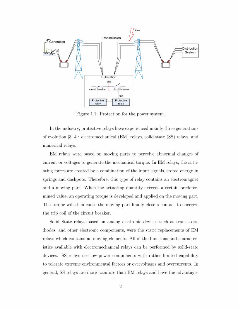
Figure 1.1: Protection for the power system.
In the industry, protective relays have experienced mainly three generations
of evolution [3, 4]: electromechanical (EM) relays, solid-state (SS) relays, and
numerical relays.
EM relays were based on moving parts to perceive abnormal changes of
current or voltages to generate the mechanical torque. In EM relays, the actu-
ating forces are created by a combination of the input signals, stored energy in
springs and dashpots. Therefore, this type of relay contains an electromagnet
and a moving part. When the actuating quantity exceeds a certain predeter-
mined value, an operating torque is developed and applied on the moving part.
The torque will then cause the moving part finally close a contact to energize
the trip coil of the circuit breaker.
Solid State relays based on analog electronic devices such as transistors,
diodes, and other electronic components, were the static replacements of EM
relays which contains no moving elements. All of the functions and character-
istics available with electromechanical relays can be performed by solid-state
devices. SS relays use low-power components with rather limited capability
to tolerate extreme environmental factors or overvoltages and overcurrents. In
general, SS relays are more accurate than EM relays and have the advantages
2

of reduced size of solid-state devices. Furthermore, absence of mechanical mov-
ing component in SS relays which may normally bring noise and cause contact
problem, and less maintenance is also an improvement compared to the elec-
tromagnetic relays.
Currently, most commercial relays are digital numeric relays based on mi-
croprocessor technology, and sequential software programmability.This type of
relay is introduced with the development of VLSI (Very Large Scale Integra-
tion) technology and fast microprocessors. The core of this type of relay is
digital signal process (DSP) microprocessor. The usual relay inputs are power
system voltages and currents. Analog signals will first be filtered and converted
to the digital form by analog-to-digital converter (ADC). Then the relaying al-
gorithm processes the sampled data to generate a digital output. The most
obvious advantage of the microprocessor-based relay is the flexibility due to
their programmable approach. Various protection functions can be provided
by numerical relays at low cast and compete with conventional relays.
Recently new types of protective relay hardware are reported in the litera-
ture. In [5] a distance protective relay implementation in a field-programmable
analog array (FPAA) is presented. This approach using a combination of FPAA
and digital technologies has the potential to provide better performance than
the present-day numerical relays; however, the use of analog blocks in the relay
may have limitations on device size, switching noise and sample-rate related
bandwidth problems compared with digital technology. In the literature, a
few works have been reported regarding hardware design of the protective re-
lay on FPGA. Reference [6] proposed a hybrid protection scheme for HVDC
(High Voltage Direct Current) line implementation, and [7] implemented the
wavelet-based directional protection for power transformer.
From the development trajectory of protective relays, objectives of speed,
reliability, flexibility improvements in the device design can be seen.
3

1.2 Motivation For This Work
The growing complexity and size of modern power systems demands faster
and better performing protective relays. Especially, the traditional notion of
power systems is mutating into the smart grid concept with the widespread
use of distributed generation and smart loads, which pose significant demands
on power system protection and security [8]-[15]. Advanced concepts such as
adaption, self-healing, wide-area monitoring, agent-based, transient operation,
parameter recognition, and artificial intelligence need computationally powerful
devices to be implemented in real-time applications [16]-[19]. There is a need
for a high-capacity, high-bandwidth protective relay that can cope with the
demand of signal processing, intelligence, and communication functions that
such advanced concepts entail.
In such applications, field programmability (FP) is a desirable feature to
have in a protective relay. A FP device, whether analog or digital, is an in-
tegrated electronic circuit whose firmware can be reprogrammed in the field
after manufacture. Currently, FPGAs (Field Programmable Gate Arrays) are
making significant inroads in many applications in industrial and commercial
systems [2, 21, 22]. The characteristics of the FPGA that are germane for its
use in protection relay application are:
• inherent parallel hard-wired architecture allowing an ultra-low latency
realization of complex algorithms;
• very large capacity devices comprised of millions of logic building blocks
to provide substantial hardware resources for even the most resource in-
tensive models and algorithms;
• mature and advanced design and development tools for rapid prototyp-
ing, and tight integration with mathematical software packages such as
Matlab/Simulink, allowing users the choices of written textual (VHDL
or Verilog), or schematic design entry methods;
4

• fast clock speeds and high-speed transceivers to communicate with exter-
nal devices.
The FPGA device uses the inherent parallelism of the hardware to increase
execution speed as well as provide higher design reliability compared with se-
quential software architecture based microprocessor technology.
1.3 Objectives
The main objective of this thesis is to realize a multifunction protective relay
hardware emulation on the FPGA. The research work need is divided into the
following parts:
• Each protective relay function’s mathematical model needs to be deter-
mined and implemented. For instance, the distance relay element within
the multifunction protective relay contains fault detection, DFT and sev-
eral other sub-modules to fulfil its function.
• The hardware emulation of the multifunction protective relay starts from
building each relay elements individually on FPGA. To achieve high per-
formance, these individual hardware modules both apply the paralleled
and pipelined computation schemes.
• Model the test power system in simulation software PSCAD/EMTDC R©
and collect fault data to validate the functions of the proposed protective
relay. Several types of faults are simulated in the software and faulted
voltage and current data are generated. The proposed relay will take in
the fault data, process the corresponding calculation and issue the trip
signal to circuit breaker.
• Analyse real-time results captured from the oscilloscope. The operating
results of the proposed hardware multifunction protection system are first
5

collected from the oscilloscope. Then the results of each relay function
are analyzed to see if they meet theoretical expectations. Optimization
of the design can be applied if needed.
1.4 Outline
The rest chapters of this thesis are outlined as follows:
• Chapter 2 presents general information about FPGA technology and the
FPGA board used for the hardware multifunction protective relay emu-
lation.
• Chapter 3 illustrates both the algorithms used (DFT, CORDIC, fault
detection, etc.) and the FPGA hardware design details of the various
modules of the distance relay.
• Chapter 4 augments the distance relay function implemented in the pre-
vious chapter to create a hardware multifunction protective relay. The
other relay functions include directional overcurrent protection, over/under
voltage protection, over/under frequency protection.
• Chapter 5 gives the conclusions of the thesis and the future work.
6

Chapter 2
Background on FPGA Design
2.1 Introduction
The FPGA is essentially a high-density array of uncommitted logic. After
manufacturing, users can directly build modular hardware infrastructure by
partitioning the implementation of the applications in the field [1]. The user-
defined designs can be quickly downloaded into the FPGA after place and route.
FPGA devices improve the circuit scale and performance of CPLD (Complex
Programmable Logic Device) which is another kind of reprogrammable logic
device. Furthermore, FPGA devices are able to handle complex, high speed
control and data processing issues. The FPGA configuration is generally speci-
fied by using a hardware description language (HDL) such as VHDL or Verilog.
Nowadays, FPGA technology is widely used in various applications: indus-
trial control applications [2], defence applications such as aircrafts, missile [20],
customer applications such as network severs, routers, screens, TVs, etc. FP-
GAs have also attached the attention of real-time modelling and simulation for
various power system and electronic equipment in recent years [21, 22, 23]. The
major FPGA vendors in the market are Xilinx R© and Altera R©. In addition to
the above advantages, FPGAs are gaining widespread use compared to DSPs
because of short time-to-market, low power consumption, access to abundant
7

IP (Intellectual Property) cores and peripheral I/Os (Input/Output). Develop-
ers can use their time efficiently to develop novel applications with the available
hardware resources.
The following sections will introduce the general FPGA architecture and
the Xilinx Virtex-7 FPGA which is utilized in this research on protective relay
design. First the general FPGA architecture is described. Then the Xilinx
Virtex-7 FPGA hardware details, design tools and design flow are discussed.
2.2 The Generic FPGA Architecture
The FPGA is generally composed of three types of configurable logic com-
ponents: configurable logic block (CLB), configurable I/O blocks, and pro-
grammable interconnections. A typical architecture of FPGA is shown in Fig-
ure 2.1.
The I/O blocks are located around the periphery of the chip, providing
programmable I/O connections. All the user-defined functional elements are
achieved by CLB that is composed of several basic logic building blocks, for ex-
ample, elementary LUTs and flip-flops circuits. These CLBs are connected to
programmable switch matrix and can implement sequential as well as combina-
torial circuits. For FPGAs, the main switch technologies are based on SRAM
(Static Random Access Memory) and antifuse [24].
2.3 The Xilinx Virtex-7 FPGA
To implement the hardware protective relay, the existing Xilinx Virtex-7 de-
velopment platform in the Real-Time Experimental Laboratory (RTX-Lab) is
chosen. The Virtex-7 FPGA significantly improved system performance and
capacity compared to previous FPGA generations, which makes it suitable for
the proposed use due to the high density fabric, DSP performance, I/O band-
8

Figure 2.1: Generic FPGA architecture and components.
width and 50% lower total power than previous generation devices.
In the following subsections, the major building components of Xilinx Virtex-
7 FPGA are presented.
2.3.1 CLBs
In the Xilinx Virtex-7 FPGA, one CLB contains a pair of slices that are com-
posed of four 6-input look-up table (LUT), eight storage elements (flip-flops
and latches), wide-function multiplexers, and carry logic as shown in Figure 2.2.
The LUTs can be configured as either a 6-input LUT with one output, or as
two 5-input LUTs with separate outputs but common addresses or logic inputs.
LUTs are used to achieve a logic function. Further down the logic hierarchy of
CLB, these basic logic elements such as LUT and registers provide the logic,
arithmetic, and ROM functions.
The CLBs are main logic resources for implementing sequential as well as
9

Figure 2.2: Virtex-7 FPGA CLB [25].
combinatorial circuits with each of them connecting to programmable switch
matrix. It is also worth to mention that FPGA device capacity is often mea-
sured in terms of logic cells, which are the logical equivalent of a classic four-
input LUT and a flip-flop. The ratio between the number of logic cells and
6-input LUTs is 1.6:1. The Virtex-7 FPGA CLB′s six-input LUT, abundant
flip-flops and latches, carry logic increase the effective capacity[25].
2.3.2 Block RAMs
Block RAMs (Random Access Memories) are the main memory resource in
Virtex-7 FPGA which are used for efficient data storage, buffering, for large
shift registers, large look-up tables, or ROMs (Read Only Memory). The block
RAM in Virtex-7 FPGA can store up to 36K bits of data and can be configured
as either two independent 18 Kb RAM, or one 36 Kb RAM. These block RAM
can be configured in single or dual-port mode as shown in Figure 2.3.
The single-port RAM has the basic data, data address, write enable and
clock inputs. The simple dual-port block RAM has one read-only port and one
10

Figure 2.3: Block RAMs in the FPGA: (a) single port RAM, (b) simple dual-port RAM, (c) true dual-port RAM.
write-only port with independent clocks. The true dual-port block RAM has
two completely independent access ports, A and B. Data can be written to or
read from either or both ports. Under the true dual-port mode, it can double
the throughput of original RAMs and can be used as FIFOs (First In First
Out) working on two different clock domains.
2.3.3 Digital Signal Processing Blocks (DSPs)
Modern FPGAs not only provide a large capacity of configurable logic gates
but also integrate embedded IP (Intellectual Property) cores, for example, DSP
blocks, to facilitate the implementation of the design.
The basic DSP element in Xilinx Virtex-7 FPGA is DSP48E1 slice. The
binary multipliers, accumulators and many other logic units within it can help
implement many complicated applications. The DSP slices have features like
full-custom, small size, high system design flexibility. Figure 2.4 shows the
basic functionality of the DSP48E1 slice [25].
11

Figure 2.4: Basic functionality of the DSP48E1 slice in Virtex-7 [25].
2.4 FPGA Design Flow
Today, most FPGA vendors provide a fairly complete set of design tools that
allow automatic synthesis and compilation from design specifications in hard-
ware languages such as Verilog or VHDL, all the way down to a bit-steam
file downloading to FPGA chips. The two popular software tools are Quar-
tus II software for Altera FPGA and ISE for Xilinx FPGA. Here since we
use the Xilinx FPGA, the Xilinx ISE software suite is used for the protective
relay hardware emulation. The applications include module design, verifica-
tion, debugging, and implementation. A typical FPGA design flow is shown in
Figure 2.5.
It mainly consists of design specification, HDL coding, behavioural simu-
lations, synthesis, implementation, static timing analysis and verification on
device.
• Design Specification: The first step to take is understanding the speci-
fications of the design. According to the customer requirements, the type
or architecture of the best suitable FPGA can be determined. Then, the
whole design can be divided into several functional parts. After func-
tional specification of a design is specified which includes each module′s
12

Figure 2.5: General FPGA application design flow.
architecture, how the data flows and the control signals behave, the de-
sign constraints should also be considered. For example, the maximum
operating frequency of the design, the delay bounds of I/O delay, etc.
Thus, the output of this step is usually a document or graph describing
the target device model,system architecture and functions and interfaces
of functional modules, and design constraints.
• HDL Coding: With the design specifications, register transfer level
(RTL) HDL codes can be written to realize the design functions. The
13

programming languages are usually Verilog HDL or VHDL. The HDL-
based design is good at dealing with large and complex design. In the RTL
level, programmer can manage the abstractions of a model in the manner
of digital signal flow. It is a high level representations and description of
a digital circuit. But the synthesis for HDL may not produce an optimal
design and thus it may affect the performance and area consumption.
• Behavioural Simulation: When the HDL code is done, the next step
is to do behavioural simulation to see if the functions of each module are
achieved. Usually, the simulation begins with the submodules. Then,
a higher level module can be simulated. This step is very basic and
important because if the simulation does not produce right outputs, the
rest of the steps would not either. And testing an error in this step costs
less than in the rest of the steps. In Xilinx ISE tools, the ISim can be
used to do the simulations.
• Synthesis: This step is to convert the high-level language (VHDL or
Verilog) description to device netlist. The netlist is basically a standard
written digital circuit schematic with logic elements, such as flip-flops,
gates, etc. Synthesis tools will check code syntax and analyze the hierar-
chy of the design for optimization.
• Implementation: This step contains translation, mapping, and place-
and-route procedures to the target device family. All the functional logics
are mapped to the target FPGAs and are routed to realize the functions.
Modern tools provides some options in this step such as size-based or
performance-based options. After the implementation, a bitstream con-
figuration file that contains the whole design can be generated.
• Static Timing Analysis: Special tools would check whether the imple-
mented design meets the timing constraints. For example, the maximum
14

clock frequency the design can be running at. If the frequency is not sat-
isfied, the critical path can be found and optimized to reach the desirable
clock frequency.
• Download and Verify: After the previous work has being done, the
design is ready to be tested on FPGA devices. The bitstream file then
can be downloaded into FPGA device. The function and outputs of the
design are tested on FPGA board to make sure if it’s functioning correctly.
Programmers may use software like ChipScope or digital oscilloscopes to
verify the outputs.
2.5 Parallel and Pipeline Design in FPGA
The two major ways to improve speed and throughput in FPGA is parallelism
and pipelining techniques. For parallelism, since FPGAs are simply fields of
programmable gates, they can be programmed into many parallel hardware
paths. Different operations can be processed at the same time and do not
have to compete for the same resources. To implement a pipeline, operation
is divided into discrete steps and wire the inputs and outputs of each step to
shift registers in a loop. The output of the final step lags behind the input by
the number of steps in the pipeline. The latency of a pipeline, measured in
clock cycles, corresponds to the number of steps in a pipeline. For a pipeline
operation with the latency of N, the first result becomes valid after N clock
cycles, and the output of each valid clock cycle lags behind the input by N-1
clock cycles.
For instance, the calculation of a × b + c × d in the FPGA hardware can
be achieved by the circuits in Figure 2.6. Assume the circuit is working under
a certain clock frequency. All the three calculation components are pipelined
and have the latency of 5 clock cycles. This means if each of the four input
numbers is given a new value at each clock cycle, each component takes initial
15

Figure 2.6: Paralleled and pipelined computation of a× b+ c× d in FPGA.
five clock cycles to generate the first calculation results. But after that, at each
clock cycle there will be a new result instead of waiting for another 5 clock
cycle. And in the whole design, a× b and c× d are computed simultaneously,
which is the parallel computation in this design. Therefore, the total latency
for the whole module is 5+5=10 clock cycles, since the two multiplications are
done in parallel. The other 5 clock cycles are occupied by the addition.
2.6 Experimental Setup
The full hardware multifunction relay design was targeted to the Xilinx Virtex-
7 XC7VX485T FPGA, using Xilinx ISE tools to synthesize and implement the
architecture. In order to observe output waveforms, a 16-bit 4-channel DAC
board is connected to the FPGA board with an FMC-DAC-Adapter. The
Tektronix 1 GHz DPO4104 with 4 analog channels and 5 GS/s mixed signal
oscilloscope is used to capture the output of the DACs (Digital-to-Analog Con-
verter) connected to the Virtex-7 FPGA. Figure. 2.7 depicts the experimental
test setup for this research work.
16

Figure 2.7: Experimental setup.
2.7 Summary
In this chapter, the fundamentals of FPGA device and the experimental setup
used in this research are presented. By following the design flow, a specific
design can be implemented on FPGA device. In addition, designers can take
advantage of parallelism and pipelining to improve speed and throughput on
the FPGA.
17

Chapter 3
Real-time Distance Protective
Relay Emulation on FPGA
3.1 Introduction
Distance protection is one of the most widely used protection functions in power
system. Its operation is based on the measurement and evaluation of the short-
circuit impedance which is proportional to the distance between the relay and
the fault location.
The distance relay1 is also the first relaying function designed in this pro-
posed multifunction relay based on FPGA. Taking the advantages of FPGA
technologies introduced in Chapter 1 and 2, a fast and reliable hardware dis-
tance relay has been emulated in this chapter. The model contains several
basic submodules such as Coordinated Rotation Digital Computer (CORDIC),
Discrete Fourier Transform (DFT), and Fault Detection to fulfil the distance
relay function.
The overall architecture of the FPGA-based hardware distance relay is
1Part of the material from this chapter has been published: Y. Wang and V. Dinavahi,“Low-latency distance protective relay on FPGA”, (IEEE Trans. on Smart Grid), pp. 1-10,Oct. 2013.
18

Figure 3.1: Overall architecture of the FPGA-based hardware distance relay:functional block diagram.
shown in Figure 3.1. There are two options of operating modes available. Op-
tion I is DFT-based distance relay for phasor signal processing which consists
of four main hardware modules: the DFT processing module, the CORDIC
processing module, the fault detection module, and the protection elements
module. In this mode, by taking in fault voltage and current data through the
I/O interface at first, the DFT module estimates fundamental amplitude and
phase of the signals. The CORDIC processing provides trigonometric and non-
linear function values that are needed for arithmetic computations. The fault
detection module utilizes the DFT results of the currents to detect the inception
of a fault based on an over-current protection mechanism, while the protection
element module calculates the fault impedance and decides the trip logic. If a
fault is detected, and the calculated impedance falls into the protection zone,
a trip signal for the associated circuit breaker is sent to isolate the fault. In
addition, a global control module is designed to control all the operations in
19

the whole design. The Option II is the instantaneous-signal-based distance re-
lay module which can process instantaneous signals to achieve a much faster
response. In the following sections, each module within the proposed relay is
discussed and its hardware design details are presented.
3.2 DFT Module with DC Offset Removal
The widely-used digital distance relay relies on the fundamental frequency com-
ponent extractions of the voltage and current signals at the relay location that
can derive the fault impedance. Ideally, these periodical voltage and current
signals in the power system are pure sinusoids at steady state. However, during
the fault, the voltage and current signals will contain large harmonics and dc
offset which distort the original waveforms. The dc offset influences the precise
relay reach and convergence speed of the fundamental frequency signal from
DFT. Therefore, a good dc offset rejection capability is expected. This section
will introduce the algorithm and FPGA implementation of the DFT with dc
offset removal module.
The very first step is to obtain the signal fundamental frequency compo-
nents. Among the existing filtering algorithms [26, 27, 28, 29, 30, 31] for the
fundamental extraction in digital distance relays, the DFT which has improved
harmonic immunity is one of the most popular methods to obtain the quantities
of interest. However, dc offset transients contained in fault signals can affect
accurate estimation of phasors through DFT. As a result, transmission line
relays tend to maloperate by overreaching or underreaching the setting value.
Therefore, the dc offset component has to be removed. Here the algorithm put
forward by [29] is adopted as it only requires one cycle plus two samples to
finish full-cycle DFT (FCDFT) calculation with dc offset removal. The effect
of the additional two calculations due to the two samples can be offset by the
low-latency of the FPGA hardware module.
20

The conventional FCDFT algorithm calculates the fundamental component
of a sinusoidal discrete time signal can be described as:
X(1) =2
N
N−1∑n=0
x(n)× (cosω1n∆T − j sinω1n∆T )
=2
N
N−1∑n=0
x(n)× (cos2πn
N− j sin
2πn
N),
(3.1)
A1 =√X2
1real +X21imag (3.2)
θ1 = arctan(X1imag/X1real) (3.3)
where x(n) is the discrete-time sinusoidal input signal, N is the number
of samples in a fundamental period, with ω1 being the fundamental angular
frequency, and ∆T the sampling interval. Then, with real and imaginary parts
of the fundamental phasor known, the amplitude A1 and phase θ1 of the phasor
could be worked out as in (3.2) and (3.3). For dc offset removal strategy, the
input signal contains a decaying dc offset Ae−t/τ (time constant τ = q∆T ).
After computing Xreal(N), Xreal(N+1), Xreal(N+2) which are real parts of three
FCDFT fundamental phasor calculation results, the parameters of the dc offset
are obtained as:
e−1/q =(Xreal(N+2) −Xreal(N+1))cos(2π/N)
(Xreal(N+1) −Xreal(N))cos(4π/N), (3.4)
A =0.5N(Xreal(N+1) −Xreal(N))
cos(2π/N)e−1/q(e−N/q − 1). (3.5)
The dc offset can be then subtracted from the sampled signal x(k) as:
z(k) = x(k)− Ae−k/q. (3.6)
It is worth to mention that, the DFT is based on a moving window strategy.
21

Figure 3.2: Pipelined floating-point DFT module with dc offset removal.
The results obtained when the window contains both pre-fault and post-fault
samples are unreliable, it is reasonable to wait until the window contains only
post-fault data to get the right relaying decisions.
Fig. 3.2 shows the FPGA hardware design of DFT module with dc offset
removal. The DFT calculation module gets the set offset control signal from
the finite state machine controller which has four transition states going from S1
to S4. Under the control strategy, the controller first senses the fault detected
signal, and waits for two more sample calculation cycles to finish dc offset
parameters calculation. Once the calculation is done, a set offset signal is sent
out to the DFT calculation module. In each DFT computation cycle, with
collection of one full-cycle window of fault data, sin and cos values, imaginary
and real part of the fundamental phasor are calculated. After taking square
root of the sum of imaginary and real part squares, and taking the arctangent
of imaginary part over real part, the amplitude and phase of the set of data are
generated. After this calculation is completed, the data window moves forward
22

by one sampling point to do the next computation cycle. Within the module,
all the computation elements use IEEE single-precision floating-point format
for higher precision and are fully pipelined to enhance throughput.
3.3 CORDIC-based Trigonometric and Non-
linear Function Evaluation Module
The trigonometric and nonlinear function values required by the DFT module
are generated from the iterative CORDIC module. The CORDIC algorithm
was first introduced by Volder for the trigonometric function computation and
later on for hyperbolic functions by Walther. The CORDIC method [32, 33, 34]
has the advantage of higher precision over the conventional look-up-table (LUT)
based method. Because usually the desired trigonometric or nonlinear function
values are stored in LUTs whose length and precision are limited by the volume
of ROM limits.
The rotation mode and vectoring mode are generally the two ways to imple-
ment the CORDIC algorithm, which result in computations of different trigono-
metric or hyperbolic functions. The general form of CORDIC iteration is as
follows:
xi+1 = xi −m · σi · yi · 2−i
yi+1 = yi + σi · xi · 2−i
zi+1 = zi − σi · αm,i
i = i+ 1.
(3.7)
In each rotation, the plane vector vi = (xi, yi)T rotates to vi+1 = (xi+1, yi+1)T .
zi tracks the angle at each rotation. For example, in the rotation mode shown
in Fig. 3.3, when estimating the trigonometric values of the given angle that is
initialized at first, zi rotates toward 0 with a micro rotation angle of θi which
23

Figure 3.3: CORDIC rotation mode for the circular coordinate system.
has the tangent value of 2−i (or hyperbolic tangent value of 2−i in hyperbolic
coordinates) in each iteration. The σi indicates the rotation direction. In the
end, when the sum of rotated angles reaches the input angle, the x and y coor-
dinates indicate the sin and cos values of the input angle. On the other hand,
in the vectoring mode the coordinates of a vector are given apriori while the
magnitude and angular argument of the original vector are computed. There-
fore, after n iterations, CORDIC module can obtain the trigonometric and
hyperbolic functions based on the mode it is operating on. The parameter de-
scriptions and the CORDIC mode operation summary are given in Table 3.1.
With the computation results of the elementary functions through CORDIC,
the nonlinear functions in (3.6) can be calculated as in (3.8) and (3.9). Taking
e−1/q in (3.6) as variable m, and k as variable n, the nonlinear function mn is
decomposed as:
mn = en∗ln(m). (3.8)
Note that the exponential function ex and natural logarithm function ln(x)
24

Table 3.1: CORDIC iteration parameter and function description
Circular coordinate Hyperbolic coordinate(m = 1) (m = −1)
Parameters α1,i = tan−1(2−i) α−1,i = tanh−1(2−i)Rotation: sin(x),zi → 0 tan−1(x)σi = sign(zi) cos(x)Vectoring: sinh(x),yi → 0 tanh−1(x)σi = −sign(xiyi) cosh(x)
Figure 3.4: FPGA design of CORDIC module in one iteration.
could be obtained from:
ex = sinh(x) + cosh(x),
ln(x) = 2tanh−1|x− 1
x+ 1|.
(3.9)
The design of the CORDIC algorithm on FPGA has a pipelined architecture
to improve speed and throughput. Fig. 3.4 shows how each CORDIC iteration
is implemented in hardware. Arctangent and hyperbolic arctangent values of
2−i are pre-calculated and stored in memory. Then, in each iteration, there are
only addition/subtraction and shifting operations (multiplication by 2−i can be
done by bit shifting to the right), which can be easily achieved in hardware. The
iterative stage n can be set manually. In this design, it is set to 20. Besides, it
is worthwhile to mention that since the iterative CORDIC algorithm based on
25

fixed-point data, all the input data which are normally in floating-point format
will be converted to fixed-point numbers using a float-to-fix module. And for
the CORDIC computation results will then be converted back to floating-point
numbers by a fix-to-float module in order to interface with other floating-point
data based modules.
3.4 Fault Detection
The fault detection module detects the initiation of the fault and trigger the
different zone timers. It is based on the over-current starting method. This
detection algorithm uses the traditional FCDFT filtering results of fundamental
amplitude to decide the detected signal. Although the algorithm suffers from
some drawbacks such as its sensitivity to even harmonics and decaying dc
components in the fault signals, the presence of harmonics does not significantly
affect the fault detection decision [35]. Fig. 3.5 shows the moving window-based
strategy. Each window contains full fundamental cycle of input signals, with
every calculation done, the window discards one old data and takes in the
next one new data to construct a new window. If the calculated fundamental
amplitude of any phase current exceeds a certain threshold value three times
consecutively, this shows that the transmission line is exposed to an abnormal
situation, and a fault detection signal is sent out.
The hardware implementation details of the fault detector are shown in
Fig. 3.6. Previous DFT amplitude results enter into the module, and are com-
pared with the threshold value. The signal enable comes from DFT module
output indicating validation of each DFT computation result. It enables the
comparison and registering process. The register inserted after the enable sig-
nal is for synchronization purpose. If three successive amplitudes exceed the
threshold, the three single-bit registers which record the comparison results will
become ‘1’. Then a fault detection signal would be generated.
26

Figure 3.5: Fault detection based on the moving window strategy.
Figure 3.6: Fault detection hardware module.
3.5 Distance Protection Elements
The FPGA-based hardware digital relay was designed to protect a three-phase
transmission line with six impedance measuring elements: three phase-to-
27

Figure 3.7: Relay characteristics with three zone protection : (a) mho charac-teristic, (b) quatrilateral characteristic.
Table 3.2: Impedance Equations Based on Different Fault Types
Relay elements Impedance formula
a-g VA/(IA + 3k0 ∗ I0)b-g VB/(IB + 3k0 ∗ I0)c-g VC/(IC + 3k0 ∗ I0)a-b (VA − VB)/(IA − IB)b-c (VB − VC)/(IB − IC)c-a (VC − VA)/(IC − IA)
I0 is zero sequence current calculated from (IA + IB + IC)/3; Z0
and Z1 are zero and positive sequence line impedances from relaylocation to protection zone respectively; k0 = (Z0 − Z1)/3Z1.
ground relays and three phase-to-phase relays. Table 3.2 presents apparent
impedance calculations for different fault types.
The impedance calculated from these six relay elements is then processed by
a mho or quadrilateral characteristic [4, 36, 37] relay element to decide which
protection region it is in. Fig. 3.7 shows the two characteristics with three
protection zones. Each protection zone covers certain length of tranmission
line. For example, zone 1 protects 80 % length of the line. Zone 2 can protect
the whole length of the line while zone 3 protects the whole line plus part of the
adjacent line. Applying different zone protection can be achieved by setting
28

different zone area of the characteristic shapes. The coordination between
different zones is achieved by setting different corresponding time delays which
are simply digital counters.
For mho characteristic, the protection element module calculates the angle
between polarizing vector Vp and operating vector Vo = IZR − Vp, where Vp
equals to fault voltage acting as reference, I is fault current and ZR is the
relay setting. As seen from Fig. 3.7 (a), if the angle between the two vectors
is greater than or equal to 90, the fault impedance locates within or on the
characteristic circle meaning the measured impedance is under reaching the
zone. Then the relay will issue a trip command to the corresponding circuit
breaker for the transmission line.
For quadrilateral characteristic shown in Fig. 3.7 (b), it is most preferred
when protecting short transmission lines as it has better resistive coverage. The
quadrilateral characteristic is determined by four straight lines in each zone.
L1 is the reactance relay setting (Xn1) and L2 is the angle-impedance relay
setting (Zn2). L3 and L4 are the directional relay with angle settings (θ1, θ2).
With all the four lines, the shape and size of the quadrilateral characteristic
model is constructed. If the apparent impedance enters into the quadrilateral
region, the relay trips.
Both the FPGA implementation of mho and quadrilateral elements can be
achieved by applying complex number computation and angle comparison [38].
At first, the impedance is calculated by a complex number division module,
for example,a+ jb
c+ jd, which is shown in Figure 3.8. In the figure, real part =
ac− bdc2 + d2
and imaginary part =bc− adc2 + d2
. For mho characteristic, with two
vectors ready, the angle between them is cosθ =vo · vp| vo || vp |
. Since the cosine
values of 90 is zero, the sign of the cosine value can be good indicator to
determine whether the fault is inside the zone. In quadrilateral zone, the
calculated impedance is compared with the four sides of the shape by checking
the relative position of impedance point and the line. It should meet the
29

Figure 3.8: Complex number division in FPGA.
conditions of locating below L1, above L4, on the left of L2 and right of L3 to
get a in-the-zone decision.
3.6 Instantaneous-Signal-Based Distance Re-
lay Element
To provide a faster tripping, this work also gives another option of distance
protection that is based on instantaneous signal processing. The basic trip
strategy of this option is the same as introduced in the previous subsection,
however, unlike the DFT distance relay option relying on the fundamental
phasor extraction illustrated before, the instantaneous-signal-based algorithm
processes instantaneous voltages and current signals [4][39]. As a result it can
shorten the operating time to less than half a fundamental cycle while the DFT
method requires collecting one full cycle of data to calculate the phasors and
then perform further protection logic. In this module, the input waveforms are
first filtered to remove any high-frequency components that could influence the
30

Figure 3.9: Instantaneous-signal-based distance relay: (a) Functional blockdiagram of the hardware design, (b) Principle of operation.
accurate decision making of the relay.
The FPGA implementation of the instantaneous-signal-based method is
shown in Fig. 3.9 (a). The filtered fault signal goes into the module and is
compared with an offset value (here set as ‘0’.) to produce a square wave
corresponding to the input sinusoidal value. The square wave carries the phase
information of the sinusoidal wave. Then, the square waves of the two input
vectors are compared with each other using a coincidence detector. A ‘-1’ is
produced during the times when both square waves agree in polarity while a
‘+1’ is produced during times the two square waves have opposite polarity; thus
a coincidence detection is achieved resulting in a double frequency square wave.
31

Table 3.3: FPGA hardware resource usage
Modules Slice Registers Slice LUTs DSP blocks(607,200 (303,600 (2800available) available) available)
DFT with 41096 (6%) 20446 (6%) 24 (1%)dc offset removalCORDIC 6429 (1%) 4946 (1%) 2 (0.07%)
Fault detection 180 (0.03%) 427 (0.1%) 0
Relay characteristics element 8421 (1%) 914 (0.3%) 12 (0.4%)
Instantaneous 7992 (1%) 1843 (0.6%) 15 (0.5%)process element
Total usage 64118 (9%) 28576 (8%) 53 (2%)
If the two input waves have a phase difference of ± 90, the double frequency
square wave has equal positive and negative pulses as in Fig. 3.9 (b) (2). In
other cases, for instance a fault, the coincidence is biased that can be clearly
seen in Fig. 3.9 (b) (1 or 3). The ACC block takes in the coincidence results and
accumulates the biased part points in the double frequency waveform. Once
the accumulation number exceeds a set threshold, a trip output signal is sent
to isolate the fault.
3.7 Case Study and Results
The entire hardware resource consumption of the distance relay design is given
in Table 3.3.
The whole design which includes the two operational options has a total
latency of 2.09µs and 0.35µs respectively based on an FPGA clock frequency
of 100MHz. According to the breakdown of each module’s latency shown in
Fig. 3.10, for the phasor-based option, the DFT module consumes the largest
latency of 83 clock cycles, while the fault detection module has the smallest
latency of 3 clock cycles. In addition, the CORDIC module, the dc offset
32

Figure 3.10: Hardware module latency breakdown for distance relay.
parameter calculation and the mho or quadrilateral relay element utilize 30,
51, and 42 clock cycles respectively. For convenience, the latency of mho and
quadrilateral element calculation was designed to be the same by adjusting the
internal elementary computing components’ latency. For instantaneous-signal-
based option, the overall latency is greatly reduced to 35 clock cycles due to the
elimination of fundamental phasor calculations. The low latencies of the design
can be attributed to the hardware parallelism and deep pipelining employed in
various hardware modules.
To test the effectiveness of proposed distance relay hardware design, several
typical faults were simulated on a test power system using PSCAD/EMTDCr
to generate the fault data. These data are then fed into the target hardware
distance relay for test and validation. The tested power system consists of two
synchronous generators and two transmission lines which are 110 km and 100
km long respectively. System is given in Fig. 3.11 with parameters given below.
Vbase = 230 kV, Sbase= 100 MVA, fault impedance = 0.01 Ω.
Source parameters: Zs=9.2+j52 Ω, Es1= 230∠0 kV, Es2= 230∠20 kV.
Line 1 length: 110 km; Line 2 length: 100 km.
33

Figure 3.11: Single line diagram of the test power system.
Transmission line sequence impedance (Ω/km): Z0 = 0.363 + j1.326, Z1 =
0.0357 + j0.5078, Z2 = 0.0357 + j0.5078.
The designed hardware distance relay was tested under four types of fault
conditions. The first fault event is a single-phase-to-ground fault which occurs
on the transmission line1 50 km away from the relay location. The oscilloscope
traces real-time simulation results of fault data transients at the relay location
are given in Fig. 3.12 from t=0.1 s to t=0.565 s. The sustained fault in phase-a
is initiated at time t1=0.28 s, when the consequent decrease in va, and increase
in ia, and its dc offset can be observed. In the DFT processing results of the
fault phase current shown in Figure 3.13, the amplitude of Segment I stays
zero until one full cycle of fault data collection is finished. During Segment II,
the ia amplitude value stays constant under normal operating condition until
at t=0.28 s when a ground fault occurred. Due to the inception of the fault,
according to the DFT calculation, the ia amplitude starts to increase after a
small transient oscillation. The fault detection module senses the abnormal
current increase and operates to send the fault detected signal at t=0.287 s.
The smooth Segment III indicates the effectiveness of the dc offset removal of
fault current in the faulted phase. As for the final tripping, the phasor-based
option gives trip signal at t=0.303 s. All the other tripping times for all fault
types can also be found in Table 3.4.
Fig. 3.14 shows the real-time trajectory of the apparent impedance seen
by the relay during the phase-to-ground fault. For the mho characteristic, the
34

Figure 3.12: Real-time fault data waveform for a single phase a to ground fault.Scale [time: 1 div x = 46.5 ms; voltage: 1 div v= 70 kV; current: 1 div i= 0.97kA.]
mho zone 1 reach is 80% of the line length, which is 3.14 + 44.69i Ω. The real-
time mho circle was obtained by coupling the time-based x and y coordinates
for the relay impedance setting, while the real-time impedance trajectory was
derived by coupling the calculated time-varying R and X signals displayed on
the oscilloscope. Before the fault at the initial state (−628.3 + j1.7 Ω), the
impedance is outside the mho characteristic circle. After the fault happens,
the impedance enters into the circle zone 1 and converges to its final state of
5.85 + j24.33 Ω, which is 56% of the zone reach and 44% of the line1 length.
After the fault detection, the relay calculates the phasor comparison criteria
and trips since the operating point is within the trip zone.
The next fault condition presented is a b-c phase-to-phase fault with fault
35

Figure 3.13: DFT results of faulted phase a, fault detection and trip signals fora phase-a-to-ground fault. Scale [time: 1 div x = 46.5 ms; dft current: 1 divi= 0.97 kA.]
Table 3.4: Trip times for different types of faults
Faults Phasor-based Instantaneous-signal-based(ms) (ms)
a-g 23.27 9.13b-c 22.45 7.35b-c-g 21.90 6.83a-b-c-g 22.30 7.25
data shown in Fig. 3.15. The b and c phase current DFT with dc offset removal
results are shown in Fig. 3.16. The fault currents of phase-b and phase-c
increase during fault and then stay at the constant values of about 7 times
of pre-fault current value. In the figure, the fault detection time and tripping
time can also be observed. The specific detection and tripping times are given
in Table 3.4 and 3.5. The locus of the apparent b-c phase impedance is given in
Fig. 3.17. The apparent impedance moves from the initial state (−630.8+j4.49
Ω), then experienced the short period of dramatic changes and finally converged
to impedance of 2.55+j25.98 Ω, which is around the 46% of the line impedance
and 58% of the zone reach.
36

Figure 3.14: Real-time impedance trajectory for a-g fault: a) Real-time resis-tance (R) and reactance (X) values with respect to time, [time: 1 div x= 46.5ms; 1 div y = 500 Ω], b) x-y mode trace of impedance.
Table 3.5: Fault detection times comparison based on different sampling rates,(DFT-based)
Faults Lower sampling Higher sampling Reduction(68/cycle), ms (334/cycle), ms ms
a-g 7.03 6.79 0.24b-c 5.45 4.83 0.62b-c-g 5.28 4.79 0.49a-b-c-g 5.06 4.54 0.52
The trip time results of a double-phase-to-ground fault and a three-phase-
to-ground fault are given in Table 3.4. According to these results, the proposed
hardware digital distance relay has achieved its fundamental objectives. While
37

Figure 3.15: Voltage and current signal of a b-c double phase fault. Scale [time:1 div x = 46.5 ms; voltage: 1 div v= 140 kV; current: 1 div i= 0.97 kA.]
Table 3.6: Fault trip times comparison based on different sampling rates,(instantaneous-signal-based)
Faults Lower sampling Higher sampling Reduction(68/cycle), ms (334/cycle), ms ms
a-g 11.03 10.2 0.83b-c 7.08 6.4 0.68b-c-g 6.86 6.33 0.53a-b-c-g 6.92 6.41 0.51
an exact comparison of the FPGA-based distance relay with existing numerical
relays might be somewhat misleading since the implemented algorithms and the
design logic might not be exactly the same, to put this work into context, a
few examples from existing relays in the industry are provided. ABB’s REL
650 line distance protection relay has the distance measuring typical operate
38

Figure 3.16: Phase b phase and phase c current DFT results, fault detectionand trip signals. Scale [time: 1 div x = 46.5 ms; dft current: 1 div i= 0.97kA.]
time of 30 ms, and 24 ms for the REL 670 platform. In SEL’s 421 protection,
automation, and control system, the high-speed elements operate around 0.5
fundamental cycle, while the standard-speed elements longest operating times
is close to 1.5 fundamental cycles. These operating times are similar to the
ones shown in Table 3.4 and Table 3.6 for the designed hardware distance relay.
This is because, using FCDFT, one can not initiate the Fourier algorithm until
a full cycle of data has been collected. Furthermore, it is worth mentioning
that the default sampling rate for this hardware design is 68 samples/cylce.
However, the overall low-latency of the hardware design leads to high-speed
computation on the FPGA, and thus higher sampling rates can be chosen
(more recent numerical relays use sampling rates that are as high as 96 samples
39

Figure 3.17: Real-time b-c phase impedance for a b-c double phase fault. a)Real-time resistance (R) and reactance (X) values with respect to time, [time:1 div x = 46.5 ms; 1 div y= 900 ohm], b) x-y mode trace of impedance.
per period [40]). In the proposed hardware design, when the sampling rate is
334 (50 µs time interval) per cycle, results in Table 3.5 for the DFT-based
and Table 3.6 for the instantaneous-signal-based options show that the fault
detection time or trip time could be shortened by over 10%.
40

3.8 Summary
In this chapter, the complete distance relay is emulated in hardware. The ma-
jor hardware modules include CORDIC, DFT with dc offset removal, fault de-
tection, distance protection elements and instantaneous-signal-based distance
relay. The algorithms have been examined and the results showed that this
relay has achieved its main functionalities.
The DFT module can eliminate the dc offset and provide more precise fun-
damental components of the input signals to decide the trip decisions. In addi-
tion, the distance relay is capable of dealing with high sampling speed due to
the low latency. As a result, the fault detection and trip time could be reduced
under a higher sampling frequency. As for the hardware resource consumption,
the distance relay only consumes 9% of the entire hardware resources which
leaves us plenty of room to add other functions and features.
41

Chapter 4
Hardware Multifunction
Protective Relay Emulation on
FPGA
4.1 Introduction
After the distance relay module has been built, by adding more functional
relay elements, a multifunction protective relay can be realized. The overall
architecture of the multifunction relay is shown in Fig. 4.1. The hardware mul-
tifunction relay consists of four major relay elements: directional overcurrent
protection element, over/under voltage protection element, distance protection
element and frequency protection element.
The following sections in this chapter will introduce the algorithms and
hardware designs of all the other protection functions except distance relay in
the multifunction protection system.
42

Figure 4.1: Overall architecture of the multifunction relay.
4.2 Directional Current Protection
4.2.1 Concept and Implementation
Overcurrent protection is a simple, cheap and fast way to apply protection to
electrical components. It is generally used for phase and ground fault protection
on low cost sub-transmission lines, distribution circuits, and industrial systems.
It can also be used for primary ground-fault protection on most distribution
lines and for ground back-up protection on most lines having pilot relaying for
primary protection [41].
The overcurrent element will operate when the currents exceed the pickup
value for a pre-determined delay time, either instantaneous, definite time or
inverse-time characteristics [42]. At the same time, overcurrent relay should
not trip overload current of the line. The basic and widely used relaying scheme
is the three-step zone tripping function. The first step zone protects about 80%
43

Figure 4.2: Directional overcurrent relaying case.
of the line. The second step zone protects the whole length of the line while the
third zone reaches into the adjacent line. In order to coordinate the tripping,
the three zones are attached with different delay times.
Fault currents on a transmission line with sources at both end or in a ring
system can flow in either direction. Therefore, it is a necessary approach to
determine the fault current direction to improve trip decision making. Direc-
tional element is then used to recognize the current directions. For example,
in a system in Fig. 4.2, for fault F1 on line 1, fault currents from both sources
come to the fault location between relay location 1 and 2. When the direction
of current is monitored, these two relays will both see positive (from bus to
line) abnormal currents flow through them. They will issue trip signals to cor-
responding circuit breakers. However, overcurrent relay at location 3 will see
the opposite current direction hence it will be blocked although it might sense
the abnormal current level. After the fault F1 being cleared, loads on Bus 1 can
still be supplied by the source s1 while loads on Bus 2 and Bus 3 be supplied
by the source s2. For fault F2, relays at location 3 and 4 see the operating di-
rection current and isolate the line 2. If there is no directional elements, either
fault F1 or F2 happening may lead to the cut-off of both transmission lines.
In such case, the loads on Bus 2 will lose electricity supply. Therefore, the
directional overcurrent relay provide the selectivity and reliability for tripping.
Based on the analysis before, the directional element is developed here to
provide current direction information for the overcurrent relay. It uses the
negative impedance seen by the relay to get the direction information.
44

At first, the symmetrical components is derived. The positive sequence,
negative sequence and zero sequence components are obtained by multiplying
a transform matrix to the original three phase signals. In three-phase electrical
power systems, symmetrical components are widely used to simplify analysis
of unbalanced three phase power systems under both normal and abnormal
conditions [43]. Take the three voltage phasor for example,
Vabc =
Va
Vb
Vc
(4.1)
The symmetrical components can be obtained as follow,
Vabc = AV012 =
1 1 1
1 α2 α
1 α α2
V0
V1
V2
(4.2)
V012 = = A−1Vabc =1
3
1 1 1
1 α α2
1 α2 α
Va
Vb
Vc
(4.3)
where the number 0, 1 and 2 stand for zero sequence, positive sequence and
negative sequence respectively. And α = 1∠120o = cos120o + jsin120o =
αcos + jαsin.
The FPGA implementation of symmetrical components components cal-
culation is given in Fig. 4.3. All the elementary complex number computing
components are floating-point number based. The registers are used to create
latencies for synchronization purpose.
For obtaining the overcurrent direction information, it is generally based
on the phase relationship of V and I. Many modern relays use the angular re-
lationships of symmetrical impedance components derived from phase voltage
and current to determine the directions. In the faulted conditions, an approx-
45

Figure 4.3: Symmetrical components calculation module on FPGA.
imate 180 degrees of impedance angle change could be observed [44, 45] for
two direction faults as shown in Fig. 4.4. For relay at A, if the reverse fault
happens, the negative sequence impedance it sees is the Z2sB + Z2line, where
Z2sB is system B’s negative impedance and Z2line is the apparent negative line
impedance. And the positive sequence impedance it sees is the reverse positive
load impedance.
The process to determine the direction is to compare the measured sequence
impedance with the window of MTA ±900. The angle setting MTA is referred
to the maximum torque angle which effectively defines the two direction phase
46

Figure 4.4: Sequence impedance differences: (a) negative sequence impedanceangle indicates the direction, (b) positive seqence impedance angle indicatesthe direction. [44].
angles. The term originally comes from electrimechanical relay and is still
widely used today. Its value could be the fault impedance angle. The forward
and reverse action areas of two direction faults are clearly seen in 4.4 (a) and
(b).
The overall FPGA design for the directional overcurrent protection is given
in Figure 4.5. Figure 4.5 (a) shows the three zone overcurrent protection de-
sign. Each protection zone has its own overcurrent setting and delay timer.
Zone III has the longest time delay. After fault being detected, any timer’s
time-up signal will activate the trip signal. Figure 4.5 (b) is the overall direc-
47

Figure 4.5: FPGA directional overcurrent protection block: (a) non-directionalthree step zone overcurrent protection, (b) overall directional overcurrent pro-tection.
tional overcurrent protection design. Only when the demands for both forward
direction element and overcurrent element is met, the relay will initiate the
relay’s final tripping.
4.2.2 Case Study
A case study is conducted in this section with single line diagram given in
Fig. 4.2. The parameters of this test system are the same as the power system
given in Chapter 3.
The studied fault is a phase-a-to-ground fault happens on line 1. The os-
48
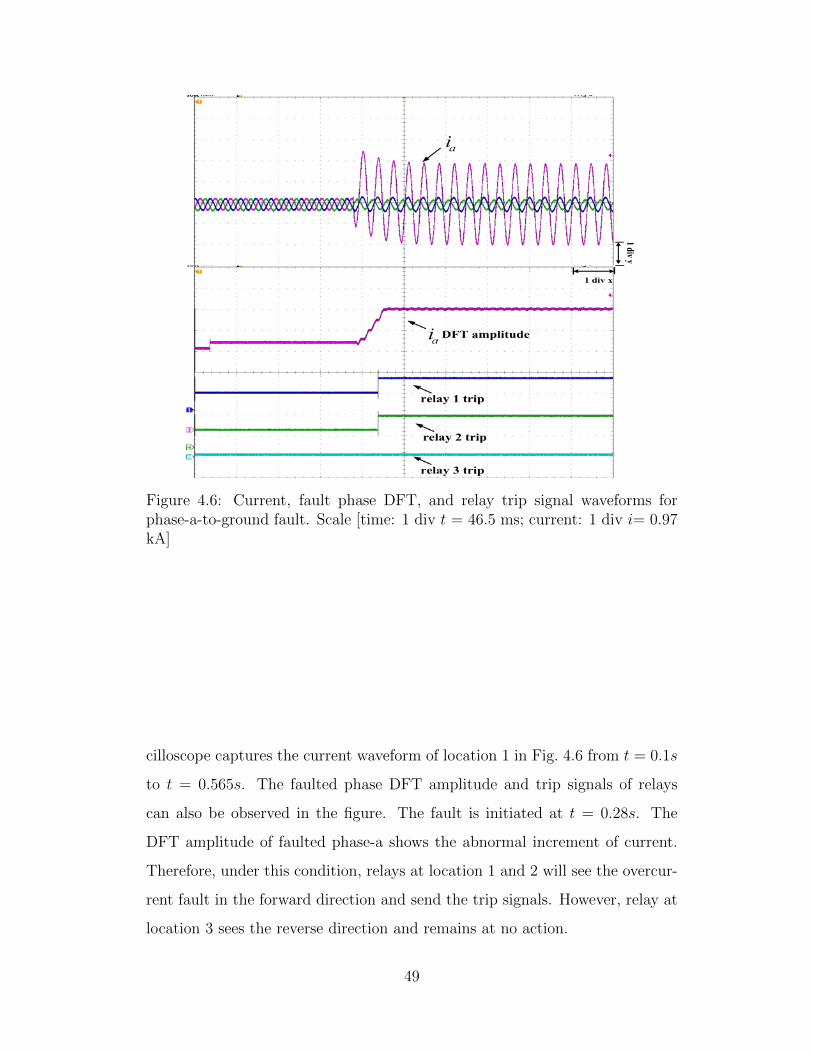
Figure 4.6: Current, fault phase DFT, and relay trip signal waveforms forphase-a-to-ground fault. Scale [time: 1 div t = 46.5 ms; current: 1 div i= 0.97kA]
cilloscope captures the current waveform of location 1 in Fig. 4.6 from t = 0.1s
to t = 0.565s. The faulted phase DFT amplitude and trip signals of relays
can also be observed in the figure. The fault is initiated at t = 0.28s. The
DFT amplitude of faulted phase-a shows the abnormal increment of current.
Therefore, under this condition, relays at location 1 and 2 will see the overcur-
rent fault in the forward direction and send the trip signals. However, relay at
location 3 sees the reverse direction and remains at no action.
49
4.3 Voltage Protection
4.3.1 Concept and Implementation
The voltage at different levels in the power system should be kept stable to
maintain the system’s normal operation. The power system voltage instability
phenomenon can lead to failure of the total or partial power system. Besides,
electrical devices in power systems are designed to operate at a certain level
of supply voltage. If voltage exceeds or drops below the device rating too
much, damages to the device can be caused. Therefore, it is very important for
protection devices to detect the abnormal voltage deviations and be capable of
isolating the corresponding faults.
This over/under voltage elements in the multifunction relay can provide
the phase-to-ground and phase-to-phase overvoltage and undervoltage protec-
tions. It can sense the abnormal voltage deviations to derive the trip signal.
The phase-to-ground undervoltage elements operate when the phase voltage is
smaller than the low setting threshold while overvoltage elements trips when
voltage is larger than the high setting threshold. The elements that deal with
phase-to-phase voltages works under the same mechanism. Any one of the three
voltages rise above or drop below a certain set value, a trip signal is generated.
This protection element also comes with the traditional three step zone protec-
tion scheme that is the same as in the overcurrent protection. Figure 4.7 shows
the hardware design of the voltage relay element with three zone protection.
The input for this element are the voltage signals. There are both high and
low threshold settings for the over and under voltage tripping decision. Each
zone has different time delay for coordination.
4.3.2 Case Study
A straightforward example is given below for a b-c double phase fault. The
power system in this case is the same as current protection case study. The
50

Figure 4.7: Voltage protection hardware design.
Figure 4.8: Voltage waveforms for a b-c phase-to-phase fault. Scale [time: 1div t = 46.5 ms; voltage: 1 div v= 140 kV]
51

Figure 4.9: DFT and trip results for a b-c phase-to-phase fault. Scale [time: 1div t = 46.5 ms; voltage: 1 div v= 140 kV]
phase-to-phase fault happens on line 1 at t=0.28 s. Fig. 4.8 shows the three
phase voltage waveforms seen by relay 1 while Fig. 4.9 depicts the voltage
amplitude of faulted phases and indicates the tripping signal. From the figure
we can see, after the fault happens, the faulted phase b and c voltage amplitudes
drop dramatically. The undervoltage element senses the decreasing in voltage
and then sends a trip signal.
4.4 Frequency Protection
4.4.1 Frequency Relay Algorithms
Frequency is one of the most important quantities in power system to evalu-
ate power quality. It reflects the balance between load and generation. Under
steady-state conditions, the total power generated by power stations is equal to
the system load and losses. Due to sudden appearance of generation-load mis-
matches the frequency can deviate from its nominal value (in North America,
it’s 60 Hz). For example, during a severe overload caused by tripping or failure
of generators or transmission lines, the power system frequency will decline.
52

Figure 4.10: Functional architecture of the frequency element.
Temporary frequency changes are an unavoidable consequence of changing de-
mand and unpredicted faulty incidents.
The frequency protection element in this multifunction relay relies on sens-
ing the abnormal frequency to make tripping decisions. It provides over/under
frequency protection with or without time delay. When the frequency pickup
value is larger than the nominal system frequency setting, the element operates
as over frequency relay. When the frequency pickup value is less than nominal
frequency, the element acts as under frequency relay.
The functional architecture of the frequency element is shown in Fig. 4.10.
The main component is the frequency estimation element which will be dis-
cussed in the following. There are many algorithms available to track system
frequency, such as DFT, FFT (Fast Fourier Transform), zero-crossing, genetic
algorithm, etc [46, 47, 48]. The algorithm for frequency estimation chosen to
implement here is in the article [47] which is based on the zero-crossing method.
The major step for frequency estimation is to measure the time interval be-
tween the two successive zero crossings of the voltage signal. Figure 4.11 shows
the strategy. At first, two successive zero-crossing points of the voltage wave-
form are found which are at t1 and t2. Then the estimated frequency can be
obtained by:
f =1
T=
1
2× (t2 − t1)(4.4)
From the above equation we can see, the accurate estimation of zero cross-
ing points is essential. The simplified cubic interpolation method [47] is applied
53

Figure 4.11: Zero-crossing method for frequency measurement.
to estimate the zero-crossings. At first, the zero-crossing points are roughly de-
tected by comparing the signs of two neighbour points. Then 5 samples around
the zero-crossing will fit the curve by using cubic interpolation (Figure 4.11).
For instance, the five sample indexes are [n − 2, n − 1, n, n + 1, n + 2], where
n and n+ 1 are the two points which have opposite signs. The cubic equation
needed to be determined is as follow,
f(x) = ax3 + bx2 + cx+ d. (4.5)
With the known five samples, the equation can be determined by least
squares method. Equation (4.6) derives the coefficients of (4.5),
A =
a
b
c
d
= (KTK)−1KTV (4.6)
where K is the constant Vandermode matrix used for least squares method and
54

V is the voltage sample vector.
K =
0 0 0 1
1 1 1 1
23 22 2 1
33 32 3 1
43 42 4 1
, V =
vn−2
vn−1
vn
vn+1
vn+2
(4.7)
After A vector is solved, the three roots of the cubic equation can be found.
One of them represents the zero-crossing point. The criteria for finding the
right root is that the number should be a real number in the section of (2,3).
The algorithm calculating for roots of the cubic equation in hardware involves
computing the eigenvalues of companion matrix of the coefficient polynomial.
At first, the companion matrix of the coefficient polynomial is formed. For
the polynomial a1x3 + a2x
2 + a3x+ a4, the companion matrix is calculated as:
B =
−a2
a1
−a3
a1
−a4
a1
1 0 0
0 1 0
(4.8)
After the companion matrix calculation, the eigenvalues calculation will
rely on iterative QR decomposition. QR algorithm, first proposed by Francis
and Kublanovskaya, is one of the most frequently used method to approxi-
mate the eigenvalues of a matrix. In the following, the implementation of QR
decomposition will be illustrated.
Let B be a m × n matrix. B matrix may be decomposed into product of
an orthogonal Q matrix and an upper triangular R matrix by Gram-Schmidt
process.
B = QR (4.9)
If the initial B matrix is there to be B0 with decomposition result of B0 =
55

Q0R0, multiplying the two matrix in reverse order can lead to a new matrix
B1 = R0Q0. Then repeat the process in an iterative way using the Gram-
Schmidt method to obtain the (n + 1)th matrix Bn+1 = RnQn. After certain
iterations, the B matrix converges to an upper triangular matrix whose diagonal
entries are the eigenvalues of matrix B. The criteria to end the iteration is to
check whether the entries below the diagonal is close enough to zero.
The Gram-Schmidt process is described as follow.
Matrix B has three columns,
B = [b1, b2, b3]. (4.10)
In the first iteration, B1 = Q1R1, the Q1 matrix can be obtained by:
e1 =u1
‖u1‖, u1 = b1
e2 =u2
‖u2‖, u2 = b2 − proje1b2
e3 =u3
‖u3‖, u3 = b3 − proje1b3 − proje2b3,
(4.11)
where ‖u1‖ stands for the norm operation of a vector and proj stands for the
projection operation : projeb =inner product < e, b >
inner product < e, e >e. And [e1, e2, e3] will
construct the Q1 matrix.
With the results from (4.11), R1 matrix can be calculated:
R1 =
< e1, b1 > < e1, b2 > < e1, b3 >
0 < e2, b2 > < e2, b3 >
0 0 < e3, b3 >
(4.12)
In the next iteration, the new B matrix equals to B2 = R1Q1.
After the eigenvalues being found, the roots of the cubic equation are de-
termined. For the frequency estimation, in each fundamental cycle, two such
roots could be found to estimate the frequency using (4.4).
56

Figure 4.12: Frequency estimation hardware module.
4.4.2 Hardware Frequency Module
The FPGA module of frequency estimation is given in Fig. 4.12. The de-
sign follows the previous illustration. Time-varying voltage signals will first go
through a 5-data-register. The register keeps tracking of five successive voltage
data. Once the approximate zero-crossing point place is detected which is in
the middle of the register, an enable signal will be sent to enable the following
submodules which are B matrix formation, root calculation and frequency cal-
culation. The realization of submodules are also shown in the Fig. 4.12. The
vector calculations in the module such as norm calculation and inner product
calculation are realized by straightforward combination of multiplications and
additions.
57

Figure 4.13: Test system for the frequency element evaluation.
4.4.3 Case Study
In this section, a case study is used to identify the effectiveness of the frequency
element. At first, a test power system shown in Figure 4.13 in PSCAD generates
the fault voltage data. The power system has three generators connected to the
bus and supply the loads. The waveform in Fig. 4.14 traces the time period
of t = 0.5s to t = 5s. The branch that can be switched on or off emulates
the frequency disturbance source. When the branch is suddenly disconnected
causing a loss of load for the generation at t = 1s, the system experiences
overfrequency condition as shown in Fig. 4.14. The system frequency gently
goes up after the disturbance and stays stable at the value of 60.90 Hz.
This real-time tracking of the system frequency in this element has a pre-
cision of ± 0.01 Hz. If the system frequency is below or above a certain level
according to specific requirements, the element can issue a signal that indicates
the abnormal situations.
58

Figure 4.14: Frequency estimation waveform. Scale [time: 1 div x = 0.45 s;voltage: 1 div v= 7.5 kV; frequency: 1 div f= 1.50 Hz.]
Table 4.1: FPGA hardware resource usage of the multifunction relay exceptdistance relay
Modules Slice Registers Slice LUTs DSP blocks(607,200 (303,600 (2800available) available) available)
Directional overcurrent 46147 (1%) 1669 (0.6%) 32 (1%)Under/over voltage 2520 (0.4%) 1417 (0.5%) 0 (0%)Under/over frequency 34983 (6%) 88,042 (29%) 510 (18%)
Total usage 81382 (7%) 91128 (30%) 542 (19%)
4.5 Summary
In this chapter, in order to form a multifunction relay, the theoretical algo-
rithms and FPGA implementations of directional overcurrent protection ele-
ment, under/over voltage element, under/over frequency element are described
and realized. Each functional hardware module is presented with a case study
to test the effectiveness of the element. From the case studies we can see, the
fundamental functionalities have been achieved.
The hardware resource usage of each element in this chapter is summarised
59

in Table 4.1. The frequency protection consumes the most hardware resource
due to the large floating point and iteration computation burden, while the
voltage protection consumes the least resource. Combined with the hardware
resource usage data of distance relay shown in the previous chapter, the overall
hardware usage still remains at a reasonable low level which can lead to lower
power consumption and longer device life cycle.
60

Chapter 5
Conclusion
In this research work, at first a hardware distance relay module was built
on the FPGA. By adding more functional relay elements such as directional
overcurrent relay element, over/under voltage relay element and over/under
frequency relay element, a multifunction protection system has been created.
All the relay submodules were developed in VHDL which can be easily
transplanted to different development environments. Taking advantages of the
inherent parallel architecture of FPGA, the proposed hardware is paralleled
and fully pipelined to achieve high operating efficiency and speed. The case
studies show the operational effectiveness of the designed relay. The advantages
of FPGA-based hardware protection design and future work are discussed in
the following sections.
5.1 Advantages of FPGA-based Hardware Re-
lay Emulation
Based on our experience with the designed hardware relay, we found the fol-
lowing advantages related to design reliability, maintainability, power consump-
tion, and flexibility that make FPGAs suitable for protective relay applications.
61

• Since the FPGA is composed of configurable logic components, all the
user-defined functional elements can be achieved by the hard-wired ar-
chitecture. Each task is allocated its own hardware resources, such as
the parallel distributed memory throughout the device, and runs inde-
pendently with less interference between two functional blocks. However,
in a numerical relay with a DSP software design, the executing algorithm
relies on transferring information to and from memory, and the sequential
process scheme. As the DSP is designed to be constantly operated for
many different tasks and its resources are shared by all tasks, it creates
lots of opportunities for the tasks to interact in unexpected ways. Con-
sequently, if a small mistakes occurs, there is high probability that the
whole program might break down. Therefore, the FPGA-based hardware
design has a higher reliability than a software program running on a DSP.
• The VHDL code for the designed hardware relay on FPGA has a modular
structure and was developed in a very clean level hierarchy. The VHDL
modules were realized in hardware circuits distributed on the chip and
connected with each other by input and output ports. The connections
between the various modules are hardwired. Testing the entire design
involved testing every functional circuit and then testing the top-level
design connected together. This makes the VHDL program very easy
to troubleshoot. There is also a lot of modern software available for
easier VHDL debugging. Users can simulate the design by tools like ISim
from Xilinx ISE to see the simulation results directly before downloading
design to the hardware. The hardware implementation results can also
be seen from software like Chipscope or be output by an oscilloscope.
• The designed FPGA-based protection system reaches low hardware la-
tency in individual module and maintains the hardware resource usage
at a reasonable level. In the distance relay module, a much higher sam-
62

ple rate can be used which leads to better reproduction of the original
signals and better transient analysis. Furthermore, new protection algo-
rithms based on transient signals can be developed on the FPGA. Even
if the DSP can perform the high resolution computation within a very
short time comparable with FPGA, it will occupy large chip resources
and heavy power consumption which can cause the device to overheat.
But in our design, with small percentage of hardware usage, the power
consumption is very low so that the life-time of the device is increased
and maintenance cost is reduced.
• The Xilinx Virtex-7 device has abundant hardware resources and periph-
eral devices. High-speed transceivers are available to communicate with
external devices for future expansion of the hardware relay functionality.
• The partial reconfiguration (PR) feature is available on the FPGA. It
can modify an operating FPGA design by loading a partial configuration
bit file, which provides the flexibility of on-site re-programming. The
partial bit files can be downloaded to modify reconfigurable regions in
the FPGA without affecting other static logic part on the board. This
feature provides us the flexibility in the choices of algorithms or protocols
available to an application.
5.2 Future Work
The research in this thesis can be extended in the following ways.
Depending on the size of the system and the real time computation require-
ment, more relay submodules and features can be replicated or added to the
same FPGA. In addition, various algorithms within this approach that are most
time- and resource- consuming can be further optimized to lower the operating
time and hardware consumption in the future.
63

The communication function is another part that could be furnished to the
existing system. In advanced substations today, the goal is to automate and
modernize the network to achieve high economy, efficiency, and safe operation.
One of most important features to achieve the goal is applying smart commu-
nication. The communication needs the data to be communicated and dealt
in a more efficient real-time mode. The FPGA technology is ideal for such
case with powerful computational and communication features such as Gigabit
Ethernet GMII. In addition, communication functions that support IEC61850
[49, 50] could be developed. Other auxiliary functions could also be included,
for example, a local Human Machine Interface for setting, data downloading
and printing.
64

Bibliography
[1] I. Kuon, R. Tessier, J. Rose, “FPGA Architecture: Survey and Challenges”,
Foundations and Trends in Electronic Design Automation, vol. 2, Issue 2,
pp.135-253, April, 2008.
[2] E. Monmasson, L. Idkhajine, M. N. Cirstea, I. Bahri, A. Tisan, M. W.
Naouar, “FPGAs in industrial control applications”, IEEE Trans. on In-
dustrial Informatics, vol.7, no.2, pp.224-243, May 2011.
[3] S. H. Horowitz, A. G. Phadke, Power system relaying, 3rd ed. , Research
Studies Press Ltd. and John Wiley & Sons, Ltd. , May 2008.
[4] ALSTOM, Network Protection & Automation Guide, 2012.
[5] M. R. D. Zadeh, T. S. Sidhu, and A. Klimek, “Field-programmable analog
array based distance relay”, IEEE Trans. on Power Delivery, vol. 24, no.
3, pp. 1063-1071, July 2009.
[6] X. Liu, A. H. Osman, and O. P. Malik, “Real-time implementation of
a hybrid protection scheme for bipolar HVDC line using FPGA”, IEEE
Trans. on Power Delivery, vol. 26, no. 1, pp. 101-108, Jan. 2011.
[7] S. P. Valsan, K. S. Swarup, “Protective relaying for power transformers
using field programmable gate array”, IET Electric Power Applications,
vol. 2, no. 2, pp. 135-143, March 2008.
65

[8] S. M. Amin, “Toward more secure, stronger and smarter electric power
grids”, IEEE PES Gen. Meeting, pp. 1-4, July 2011.
[9] D. Anderson, C. Zhao, C. Hauser, V. Venkatasubramanian, D. Bakken, A.
Bose, “A virtual smart grid”, IEEE PES Mag., vol. 10, no. 1, pp. 49-57,
Jan.-Feb. 2012.
[10] P. McLaren, O. Nayak, J. Langston, M. Steurer, M. Sloderbeck, R. Meeker,
X. Lin, M. Yu, P. Forsyth, “Testing the “smarts” in the smart T & D grid”,
IEEE Power Systems Conf. and Expo. (PSCE), pp. 1-8, March 2011.
[11] R. Podmore, M. R. Robinson, “The role of simulators for smart grid
development”, IEEE Trans. on Smart Grid, vol. 1, no. 2, pp. 205-212,
Sept. 2010.
[12] H. Qi, X. Wang, L. M. Tolbert, F. Li, F. Z. Peng, P. Ning, M. Amin,
“A resilient real-time system design for a secure and reconfigurable power
grid”, IEEE Trans. on Smart Grid, vol. 2, no. 4, pp. 770-781, Dec. 2011.
[13] F. Li, W. Qiao, H. Sun, H. Wan, J. Wang, Y. Xia, Z. Xu, P. Zhang,
“Smart transmission grid: vision and framework,” IEEE Trans. on Smart
Grid, vol.1, no.2, pp.168-177, Sept. 2010.
[14] L. Yang, P. A. Crossley, A. Wen, R. Chatfield, J. Wright, “Performance
assessment of a IEC 61850-9-2 based protection scheme for a transmission
substation,” 2011 2nd IEEE PES International Conference and Exhibition
on Innovative Smart Grid Technologies (ISGT Europe), pp.1-5, 5-7 Dec.
2011.
[15] L. Wang, J. Suonan; S. He, G. Song, “The development and perspective
of relay protection technology,” Innovative Smart Grid Technologies - Asia
(ISGT Asia), 2012 IEEE, pp.1-4, 21-24 May 2012.
66

[16] R.J. Yinger, S.S. Venkata, V.A. Centeno, “Southern California Edison’s
advanced distribution protection demonstrations,” IEEE Trans. on Smart
Grid, pp.1012-1019, June 2012.
[17] H. Liu, X. Chen, K. Yu, Y. Hou, “The control and analysis of self-healing
urban power grid,” IEEE Trans. on Smart Grid, vol.3, no.3, pp.1119-1129,
Sept. 2012.
[18] P. Mahat, Z. Chen, B. Bak-Jensen, C. L. Bak, “A simple adaptive overcur-
rent protection of distribution systems with distributed generation,” IEEE
Trans. on Smart Grid, vol.2, no.3, pp.428-437, Sept. 2011.
[19] J. F. Borowski, K. M. Hopkinson, J. W. Humphries, B. J. Borghetti,
“Reputation-based trust for a cooperative agent-based backup protection
scheme,” IEEE Trans. on Smart Grid, vol.2, no.2, pp.287-301, June 2011.
[20] W. Wang, S. Yang, J. Zhang, M. Sun, “The Design of Test System for
Launcher Equipment of One Air Defence Missile Based on FPGA”, 2011
First International Conference on Instrumentation, Measurement, Com-
puter, Communication and Control, pp.622-625, Oct. 2011.
[21] Y. Chen , V. Dinavahi, “Digital hardware emulation of universal machine
and universal line models for real-time electromagnetic transient simula-
tion”, IEEE Trans. on Ind. Electr., vol.59, no.2, pp.1300-1309, Feb. 2012.
[22] Y. Chen, V. Dinavahi, “Multi-FPGA digital hardware design for de-
tailed large-scale real-time electromagnetic transient simulation of power
systems”, IET Trans. on Generation, Transmission and Distribution, vol.7,
no.5, pp.451-463, May 2013.
[23] G. G. Parma and V. Dinavahi, “Real-time digital hardware simulation of
power electronics and drives”, IEEE Trans. on Power Delivery, vol. 22,
no. 2, pp. 1235-1246, April 2007.
67

[24] Stephen Brown and Jonathan Rose, “Architecture of FPGAs and CPLDs:
A Tutorial”, http://www.eecg.toronto.edu/ jayar/pubs/brown/survey.pdf.
[25] Xilinx Virtex-7 user guide, Xilinx Inc., 2013.
[26] A. A. Girgis, “A new kalman filtering based digital distance relay”, IEEE
Trans. on Power Apparatus and Systems, vol. PAS-101, no. 9, pp. 3471-
3480, Sept. 1982.
[27] H. J. Altuve Ferrer, I. Diaz Verduzco, and E. Vazquez Martinez, “Fourier
and Walsh digital filtering algorithms for distance protection”, IEEE Trans.
on Power Systems, vol. 11, no. 1, pp. 457-462, Feb. 1996.
[28] N. T. Stringer, “The effect of DC offset on current-operated relays”,
IEEE Trans. on Industry Applications, vol. 34, no. 1, pp. 30-34, Jan./Feb.
1998.
[29] J. C. Gu, S. L. Yu, “Removal of DC offset in current and voltage signals
using a novel Fourier filter algorithm”, IEEE Trans. on Power Delivery,
vol. 15, no. 1, pp. 73-79, Jan. 2000.
[30] T. S. Sidhu, X. Zhang, F. Albasri, and M. S. Sachdev, “Discrete-fourier-
transform-based technique for removal of decaying DC offset from phasor
estimates”, IEE Proc. Gen., Trans. and Distrib., vol. 150, no. 6, pp. 745-
752, Nov. 2003.
[31] A. H. Osman, O. P Malik, “Transmission line distance protection based
on wavelet transform”, IEEE Trans. on Power Delivery, vol. 19, no. 2, pp.
515-523, Apr. 2004.
[32] J. E. Volder, “The CORDIC trigonometric computing technique”, IRE
Trans. on Electronic Computers, vol. EC-8, no. 3, pp. 330-334, Sept. 1959.
[33] J. S. Walther, “A unified algorithm for elementary functions”, AFIPS
Spring Joint Computer Conf., vol. 38, pp. 379-385, 1971.
68

[34] Y. H. Hu, “CORDIC-based VLSI architectures for digital signal process-
ing”, IEEE Signal Processing Magazine, vol. 9, no. 3, pp. 16-35, July
1992.
[35] T. S. Sidhu, X. Zhang, and V. Balamourougan, “A new half-cycle phasor
estimation algorithm”, IEEE Trans. on Power Delivery, vol. 20, no. 2, pp.
1299-1305, Apr. 2005.
[36] A. Apostolov and B.Vandiver, “On the standardization of distance char-
acteristics”, Power Systems Conference: Advanced Metering, Protection,
Control, Communication, and Distributed Resources, pp.209,212, 13-16
March 2007.
[37] Y.G. Paithankar and S.R. Bhide, Fundamentals of Power System Protec-
tion, PHI Learning Pvt. Ltd., 2010.
[38] E.O. Schweitzer, III, Jeff Roberts, Distance Relay Element Design,
Schweitzer Engineering Laboratories, Inc, 1993.
[39] P. M. Anderson, Power System Protection, New York : McGraw-Hill :
IEEE Press, 1999.
[40] Understanding microprocessor-based technology applied to relaying,
Power System Relaying Committee, Report of Working Group I-01, Jan.
2009.
[41] GE Digital Energy, “Line Protection with Overcurrent Relays”,
http://www.gedigitalenergy.com/multilin/notes/artsci/art13.pdf.
[42] J. L. Blackburn, T. J. Domin, Protective Relaying Principles and Appli-
cations, Third Edition, Taylor and Francis Group, LLC., 2006.
[43] J. Duncan Glover, Mulukutla S. Sarma and Thomas J. Overbye, Power
System Analysis and Design, Cengage Learning, 2012.
69

[44] J. Horak, “Directional overcurrent relaying (67) concepts,” 59th Annual
Conference for Protective Relay Engineers, pp.13, 2006.
[45] K. Zimmerman; D. Costello, “Fundamentals and improvements for direc-
tional relays,” 2010 63rd Annual Conference for Protective Relay Engineers,
pp.1-12, March 29 2010-April 1 2010.
[46] M. M. Begovic, P. M. Djuric, S. Dunlap, A. G. Phadke, “Frequency Track-
ing in Power Networks in The Presence of Harmonics,” IEEE Transactions
on Power Delivery, pp.480-486, Apr. 1993.
[47] S. Y. Xue and S. X. Yang, “Accurate and Fast Frequency Tracking for
Power System Signals,” IEEE International Conference on Systems, Man
and Cybernetics, pp.2754-2759, Oct. 2007.
[48] D. V. Coury, A. C. B. Delbem, J. R. de Carvalho, M. Oleskovicz, E.
V. Simoes, D. Barbosa, T. V. da Silva, “Frequency Estimation Using a
Genetic Algorithm With Regularization Implemented in FPGAs,” IEEE
Transactions on Smart Grid, vol.3, no.3, pp.1353-1361, Sept. 2012.
[49] K. Tang, “Design and Implementation of IEC61850 for Power Generating
Plant Protection, Control and Automation,” 2010 International Conference
on Power System Technology (POWERCON), pp.1-7, Oct. 2010.
[50] D. Westermann, M. Kratz, “A Real-Time Development Platform for the
Next Generation of Power System Control Functions,” IEEE Transactions
on Industrial Electronics, vol.57, no.4, pp.1159-1166, April 2010.
70