universita degli studi di milano facolt a di scienze ... · universita degli studi di milano facolt...
TRANSCRIPT

UNIVERSITA DEGLI STUDI DI MILANO
Facolta di Scienze Matematiche, Fisiche e Naturali
&
UNIVERSITA CATTOLICA DEL SACRO CUORE
Facolta di Scienze Matematiche, Fisiche e Naturali
DOTTORATO DI RICERCA IN FISICA, ASTROFISICA E
FISICA APPLICATA
Electronic structure of TiO2 thin films and
LaAlO3-SrTiO3 heterostructures: the role of
titanium 3d1 states in magnetic and transport
properties
Settore scientifico disciplinare FIS/03
Coordinatore: Prof. Marco Bersanelli
Tutore: Prof. Luigi Sangaletti
Tesi di Dottorato di:
Giovanni Drera
Ciclo XXIV
Anno Accademico 2010-2011
arX
iv:1
210.
8000
v1 [
cond
-mat
.str
-el]
30
Oct
201
2

to Luisa, Francesco and Martina
my Best PhD achievements.

Contents
1 Introduction 5
1.1 The TiO2−δ magnetism . . . . . . . . . . . . . . . . . . . . . . 6
1.2 The conductivity of the LaAlO3-SrTiO3 interface . . . . . . . 7
1.3 Thesis outline . . . . . . . . . . . . . . . . . . . . . . . . . . . 9
1.4 Publications . . . . . . . . . . . . . . . . . . . . . . . . . . . . 10
1.5 Acknowledgements . . . . . . . . . . . . . . . . . . . . . . . . 12
2 Experimental and theoretical details 13
2.1 Introduction . . . . . . . . . . . . . . . . . . . . . . . . . . . . 13
2.2 XPS and AR-XPS . . . . . . . . . . . . . . . . . . . . . . . . 14
2.2.1 Experimental set-up . . . . . . . . . . . . . . . . . . . 15
2.2.2 XPS theory . . . . . . . . . . . . . . . . . . . . . . . . 16
2.2.3 Angle resolved XPS . . . . . . . . . . . . . . . . . . . . 19
2.3 XAS . . . . . . . . . . . . . . . . . . . . . . . . . . . . . . . . 22
2.3.1 Experimental set-up . . . . . . . . . . . . . . . . . . . 23
2.3.2 XAS theory . . . . . . . . . . . . . . . . . . . . . . . . 25
2.4 Multiplet effects on core-levels spectroscopies . . . . . . . . . . 26
2.5 Resonant Photoemission . . . . . . . . . . . . . . . . . . . . . 29
2.6 Ab-initio electronic structure calculations . . . . . . . . . . . . 36
2.6.1 Hartree-Fock method . . . . . . . . . . . . . . . . . . . 37
2.6.2 Density Functional Theory . . . . . . . . . . . . . . . . 38
2.6.3 Computing details . . . . . . . . . . . . . . . . . . . . 41
3 TiO2−δ Resonant photoemission 45
3.1 Introduction . . . . . . . . . . . . . . . . . . . . . . . . . . . . 45
3.2 Resonant Photoemission on TiO2 . . . . . . . . . . . . . . . . 47
3.3 Theoretical calculations for ResPES . . . . . . . . . . . . . . . 47
3.4 Experimental details and results . . . . . . . . . . . . . . . . . 50

4 CONTENTS
4 Magnetism in TiO2−δ and N:TiO2−δ films 59
4.1 Introduction . . . . . . . . . . . . . . . . . . . . . . . . . . . . 59
4.2 Growth method and characterization . . . . . . . . . . . . . . 63
4.3 Magnetic characterization . . . . . . . . . . . . . . . . . . . . 64
4.4 XPS measurements . . . . . . . . . . . . . . . . . . . . . . . . 71
4.5 ResPES on TiO2−δ and N-doped TiO2−δ . . . . . . . . . . . . 73
4.6 Theoretical models . . . . . . . . . . . . . . . . . . . . . . . . 82
4.6.1 DFT on TiO2 supercells . . . . . . . . . . . . . . . . . 83
4.7 Conclusions . . . . . . . . . . . . . . . . . . . . . . . . . . . . 87
5 The LaAlO3-SrTiO3 heterostructure 91
5.1 Introduction . . . . . . . . . . . . . . . . . . . . . . . . . . . . 91
5.2 XPS data . . . . . . . . . . . . . . . . . . . . . . . . . . . . . 94
5.3 XAS and XLD . . . . . . . . . . . . . . . . . . . . . . . . . . 104
5.4 ResPES . . . . . . . . . . . . . . . . . . . . . . . . . . . . . . 107
5.4.1 First data set . . . . . . . . . . . . . . . . . . . . . . . 108
5.4.2 Second data set . . . . . . . . . . . . . . . . . . . . . . 111
5.5 AR-XPS measurements . . . . . . . . . . . . . . . . . . . . . . 121
5.6 Conclusions . . . . . . . . . . . . . . . . . . . . . . . . . . . . 132
Bibliography 136

Chapter 1
Introduction
The transition metal oxides (TMO (1)) play a fundamental role in a wide
range of technological applications. They are used as dielectrics, gate insu-
lators and for magnetic applications. The transition metal oxides surfaces (2)
have a primary importance in catalytic processes, in gas-sensing, in fuel-cells
and in solar panels. Their conduction properties (3) range from insulators to
semiconductors and metals, sometimes in the same compounds. This is the
case of the so called Metal-to-Insulator transition, in which a material can
change from an insulator to a metal state upon suitable doping or under the
application of an external pressure.
In each and every of these cases, much of the relevant physics is due to
the complexity of the TM electronic structure, which still poses challenging
problems to the physics community. In fact, while the electronic structures
of elemental TM’s have already been fairly described, the same cannot be
stated for the TM oxides. The electron-electron interaction in the TM partly
filled 3d shell can induce complex correlation effects, hardly described with
the simple theories of the early solid state physics. For instance, the best
known empirical Hamiltonian that should describe the correlation aspect of
these systems, the Hubbard model, cannot still be solved exactly though it
has been introduced 50 years ago.
The complexity of the TM-oxides resides also in their bulk and surface
crystal structure. Planar dislocations, point defects, cationic or oxygen va-
cancies are often present in TMO crystals, but their positions in the lattice
can be hardly controlled. The theoretical calculations on defect sites in TMO
are also rather complex, due to the aforementioned correlation effects. Much
of the effort of experimental and theoretical physicists (and chemists) is thus

6 Introduction
devoted to the characterization and to the control of these defects.
The present thesis is focussed on the Ti-O bond in TiO2 based systems,
namely TiO2−δ thin films and LaAlO3-SrTiO3 heterostructures. The atten-
tion on these system has been drawn by the occurrence of unexpected phys-
ical properties in formally 3d0 insulators: magnetism and 2D conductivity,
respectively. Both properties are thought to be related to the 3d level pop-
ulation of titanium cations. In the following, a brief introduction to these
topics is provided.
1.1 The TiO2−δ magnetism
A peculiar case treated in this Thesis work, is the titanium dioxide (TiO2).
This system is a formally simple d0 oxide, a transparent insulator (the gap is
nearly 3 eV) widely applied in pigments, cosmetics and coatings because it is
cheap, highly refractive and bio-compatible. Due to the vastity of published
literature and to the easiness in the growth, its surface is considered as the
prototype (4) of the metal-dioxide systems. The various surface terminations
of TiO2 single-crystal are very important for catalysis applications and are
still subject of an intensive research work.
Titanium dioxide has also been claimed to be a room-temperature ferro-
magnet upon transition-metal doping (5). Even if at the beginning the dopant
ions were considered as the source of the ferromagnetism (since pristine TiO2
is diamagnetic), the researcher shifted their attention to the electronic states
generated by the oxygen vacancies. In fact, the same kind of (weak) mag-
netism have been recently measured in formally undoped samples; this phe-
nomenon is known as d0 magnetism (6) and has been found also in HfO2(7),
SnO2, ZnO, MgO and MgAl2O4(8). Each of these materials, when grown with
state-of-the-art methods, are diamagnetic. The introduction of defects that
occurs in non-equilibrium growth techniques seems to induce the observed
ferromagnetism.
However, the claim of intrinsic room-temperature ferromagnetism in these
closed-shell oxides has not yet been universally accepted by the researcher
community (9), with the most important objection being related to sample
quality (i.e. to possible external contaminations). A fine control of growth
and characterization is then necessary when dealing with the magnetism of
these materials.
The defect-related electronic states in these oxides are usually too weak

1.2 The conductivity of the LaAlO3-SrTiO3 interface 7
to be probed with standard X-ray photoemission (XPS). One of the ex-
perimental techniques that can properly address this problem is Resonant
Photoemission spectroscopy (ResPES), in which the valence band spectra
are collected by tuning the photon energy close to a selected atomic shell
absorption edge. In the case of TiO2, ResPES can enhance the titanium
electronic states in the valence band and, if present, also in the band gap.
In the first part of this Thesis, a comprehensive magnetic characterization
in a set of TiO2 samples is given, together with the analysis of Ti 3d-related
states. A series of TiO2−δ films have been grown with the RF-sputtering tech-
nique on various non-magnetic substrates; subsequently, a protocol of anneal-
ing procedures has been applied in order to alter the sample stoichiometry. A
full magnetic, crystalline and electronic structure characterization has been
carried out at each step of the films treatments. A set of N-doped TiO2−δ
thin films have also been grown, in order to verify the effect of the N dop-
ing in the TiO2 magnetism. The electronic states related to the presence of
defects in these films have been further investigated through ResPES. The
hypothesis of a clustered VO origin of the FM is further discussed in the light
of the experimental and theoretical results.
1.2 The conductivity of the LaAlO3-SrTiO3
interface
Another interesting oxide system in which the stoichiometry of Ti ions
play a fundamental role is the LaAlO3-SrTiO3 interface (LAO-STO in short).
LAO and STO, separately, are two band insulators, with an empty shell
electronic structure (3d0 for STO, 4f0 for LAO) and a similar perovskite
structure; however, the interface created by growing LAO on the top of STO
(001) has found to become metallic, hosting a quasi-2D electron gas (10). This
heterostructure becomes conductive when the STO is terminated with the
TiO2 plane while remain insulating with the SrO plane termination; the Ti-
related electronic states are thus expected to carry the metallic states.
The transition from the insulating to the metallic state is observed only
for a LAO capping larger than 4 unit cells, making the puzzle of the conduc-
tivity even more complicated. Furthermore, in some cases a low Tc super-
conductivity and isolated magnetic moments have also been detected, but
not at the same time in a sample. As in the case of the TiO2 magnetism, the

8 Introduction
growth conditions and the oxygen stoichiometry are crucial in the physics of
the LAO-STO system (11). In fact the interfaces grown in a low partial pres-
sure of oxygen yield a 3D conductivity, induced by the presence of oxygen
vacancies. Besides, STO itself is an interesting case of defect-induced physi-
cal properties: superconductivity (12) has been observed in defected SrTiO3−δ,
obtained by the annealing of pristine SrTiO3. The possibility of growing high
quality samples has been related to the detection of the anomalous Shubnikov
de Haas effect (13) in these interfaces, which is a clear proof of the 2D nature
of the conductive layer.
Different mechanisms have been invoked in order to explain the physical
phenomena in the LAO-STO heterostructures. By recognizing that the polar
nature of LAO could induce a diverging electric potential, an electronic re-
construction mechanism has been proposed, based on a charge-transfer from
the surface to the Ti atoms at the interface (14). However, there are several
proof of cationic disorder, i.e. of a non-abrupt LAO-STO interface (15); the
polar discontinuity could then be energetically relaxed by the disorder and
not by the electronic reconstruction. Finally, also the VO’s should be taken
into account, as well as the possible charge transfer effects from surface de-
fects (16). Each of these mechanisms don’t exclude the others; at the moment
there is not a general consensus in the researcher community.
As in the case of TiO2, a direct experimental proof of the conductive
electronic states can be hardly obtained with conventional photoemission
techniques. The main difficulty is the surface sensitivity of the soft X-ray
photoemission, since the relevant electronic states are buried beneath the
LAO capping. Moreover, even when hard X-ray photoemission is used, the
titanium contribution to valence band spectra is usually overwhelmed by the
oxygen 2p states. In a similar way of d0 ferromagnetism, the resonant pho-
toemission taken at Ti edge could be the best technique to directly measure
the Ti contribution to the conductivity (17).
The second part of this Thesis work is devoted to the characterization of
conductive and insulating LAO-STO interfaces, carried on with X-ray pho-
toemission (XPS), X-ray absorption (XAS) and with ResPES techniques.
The stoichiometry of each atomic species has been evaluated by compari-
son with LAO and STO single crystals. A resonance enhancement of the
conductive Ti states, associated to a small fraction of Ti3+ ions is reported
and compared to theoretical calculations. In addition, a characterization of
the intermixing and the disorder at the LAO-STO interface has been done

1.3 Thesis outline 9
through angle-resolved XPS, which in this case has required a careful control
over the theoretical model and over the experimental data handling. The re-
sults are then compared to the theoretical models proposed in the literature.
1.3 Thesis outline
In Chapter 2 the experimental and the computational details that con-
cern the X-ray spectroscopies of interest are presented. When possible, the
XPS, XAS and ResPES spectra have been compared with theoretical calcu-
lations; in this Chapter a brief introduction of the multiplet theory and the
ab-initio density functional theory (DFT) is thus given. The Hubbard cor-
rection to these models, the charge-transfer multiplet and the DFT+U, have
been adopted to calculate the spectral weight and to interpret the experi-
mental results. Finally, a section of this Chapter is dedicated to the theory
of the AR-XPS spectroscopy, applied to the LAO-STO interface.
A detailed description of the ResPES spectra at Ti L2,3-edge in pure TiO2
is given separately in Chapter 3; these data can be used as a reference
for the experimental results given in the following chapters. The XAS and
ResPES results have been interpreted both with multiplet and with DFT+U
calculations.
In Chapter 4, the photoemission and magnetization data for a series of
TiO2 and nitrogen doped TiO2 films are shown. The samples have been thor-
oughly characterized with X-ray diffraction, Raman spectroscopy, SQUID
magnetometer and XPS at each step of annealing treatments aimed to con-
trol the density of defects in the films. XAS and ResPES have also been
performed on the thinnest TiO2−δ and N-doped TiO2−δ films. The role of
nitrogen in magnetism is further explained with spin-resolved DFT calcula-
tions.
Finally in Chapter 5 the XPS, XAS and ResPES data taken on the
LAO-STO samples are shown, compared to the single-crystal LaAlO3 and
SrTiO3. The experimental results of insulating and conductive samples are
compared. The angle-resolved X-ray photoelectron spectroscopy (AR-XPS)
and X-ray photoelectron diffraction (XPD) techniques have been used to
check the structural properties of the interface and the capping layer.

10 Introduction
1.4 Publications
Here is the list of the articles already published (†) or in preparation (‡)related to this Thesis work:
1. ‡M. C. Mozzati, G. Drera, L. Malavasi, Y. Diaz-Fernandez, P. Galinetto
and L. Sangaletti; A systematical study of magnetism in TiO2−δ thin
films grown by RF-sputtering, in preparation.
2. ‡ G. Drera, G. Salvinelli, J. Huijben, M. Huijben, G. Rijnders, D. H.
A. Blank, H. Hilgenkamp, A. Brinkman and L. Sangaletti; Growth
condition effects on the basic electronic properties of LaAlO3, SrTiO3
and LaAlO3-SrTiO3 heterostructures, in preparation.
3. ‡ G. Drera, G. Salvinelli, J. Huijben, M. Huijben, G. Rijnders, D. H.
A. Blank, H. Hilgenkamp, A. Brinkman and L. Sangaletti; Origin of
titanium 3d1 electronic states in insulating and conductive LaAlO3-
SrTiO3 heterostructures, in preparation.
4. ‡ G. Drera, G. Salvinelli, J. Huijben, M. Huijben, G. Rijnders, D. H.
A. Blank, H. Hilgenkamp, A. Brinkman and L. Sangaletti; Unveiling
cation intermixing effects in LaAlO3-SrTiO3 interfaces by AR-XPS ex-
periments, in preparation.
5. ‡ G. Drera, L. Malavasi, Y. Diaz-Fernandez, F. Bondino, M. Malves-
tuto, M.C. Mozzati, P. Galinetto and L. Sangaletti; Origin, excita-
tion dynamics, and symmetry of the insulating TiO2−δ electronic states
probed by resonant photoelectron spectroscopies, revised version sub-
mitted to Phys. Rev. Lett.
6. † G. Drera, F. Banfi, F. Federici Canova, P. Borghetti, L. Sangaletti,
F. Bondino, E. Magnano, J. Huijben, M. Huijben, G. Rijnders, D.H.A.
Blank, H. Hilgenkamp and A. Brinkman; Spectroscopic evidence of in-
gap states at the SrTiO3/LaAlO3 ultrathin interfaces, Appl. Phys Lett.
98 (2011), 052097.
7. †G. Drera, M.C. Mozzati, P. Galinetto , Y. Diaz-Fernandez, L. Malavasi,
F. Bondino, M. Malvestuto and L. Sangaletti; Response to “Comment
on ‘Enhancement of room temperature ferromagnetism in N-doped
TiO2−x rutile: Correlation with the local electronic properties’ ”, Appl.
Phys Lett. 97 (2010), 186102.

1.4 Publications 11
8. †G. Drera, M.C. Mozzati, P. Galinetto , Y. Diaz-Fernandez, L. Malavasi,
F. Bondino, M. Malvestuto and L. Sangaletti; Enhancement of room
temperature ferromagnetism in N-doped TiO2−x rutile: Correlation
with the local electronic properties,Appl. Phys Lett. 97 (2010), 012506.
9. † F. Rossella, P. Galinetto, M. C. Mozzati, L. Malavasi, Y. Diaz Fer-
nandez, G. Drera and L. Sangaletti; TiO2 thin films for spintronics
application:a Raman study, J. Raman Spec. 41 (2010), 558-565.
Other publications related to magnetism and X-ray spectroscopy tech-
niques applied to diluted magnetic oxides and semiconductors:
1. L. Sangaletti, M. C. Mozzati, G. Drera, V. Aguekian, L. Floreano, A.
Morgante, A. Goldoni and G. Karczewski; Local electronic properties
and magnetism of (Cd,Mn)Te quantum wells, Appl. Phys. Lett. 96
(2010), 142105.
2. L. Sangaletti, A. Verdini, S. Pagliara, G. Drera, L. Floreano, A. Goldoni
and A. Morgante; Local order and hybridization effects for Mn ions
probed by resonant soft X-ray spectroscopies: the Mn:CdTe(110) sur-
face revisited, Phys. Rev. B 81 (2010), 245320.
3. L. Sangaletti, G. Drera, E. Mangano, F. Bondino, C. Cepek, A. Sepe
and A. Goldoni; Atomic approach to core-level spectroscopy of delo-
calized system: Case of ferromagnetic metallic Mn5Ge3, Phys. Rev. B
81 (2010), 085204.
4. L. Sangaletti, F. Federici Canova, G. Drera, G. Salvinelli, M. C. Moz-
zati, P. Galinetto, A. Speghini and M. Bettinelli; Magnetic polaron
percolation on a rutile lattice: A geometrical exploration in the limit
of low density of magnetic impurities, Phys. Rev. B 80 (2009), 033201

12 Introduction
1.5 Acknowledgements
The author wishes to acknowledge the (numerous) people involved in this
Thesis work:
• Maria Cristina Mozzati, Pietro Galinetto, Yuri Diaz-Fernandez and
Lorenzo Malavasi of the Universita di Pavia for their (enormous) work
on the growth and characterization of the ferromagnetism in TiO2;
• Alexander Brinkmann and co-worker, for the growth and characteri-
zation of the LAO-STO heterostructures at the University of Twente,
Enschede (The Netherlands);
• Federica Bondino, Elena Magnano, Marco Malvestuto and the staff of
the BACH beamline at the ELETTRA synchrotron (Basovizza, Tri-
este);
• Aleberto Verdini, Luca Floreano and Alberto Morgante and the staff
of the ALOISA beamline at the ELETTRA synchrotron.
• Luigi Sangaletti, Patrizia Borghetti, Dash Sibashisa, Filippo Federici
Canova and Gabriele Salvinelli of the Surface Science and Spectroscopy
Lab. of the Universita Cattolica di Brescia.
The work on magnetic oxides has been partly funded by the Cariplo Foun-
dation.
Finally, I wish to express my gratitude to professor Ralph Claessen for his
refereeing work and to dr. Maddalena Drera for the meticulous proofreading.

Chapter 2
Experimental and theoretical
details
2.1 Introduction
A relevant part of this thesis work have been devoted to explore in details
some core-level based X-ray spectroscopic techniques. The main advantage
of using X-rays is the possibility to be chemically selective and thus have
access to the electronic structure of a single ionic species. The experimental
methods applied in this work are X-ray photoemission (XPS), absorption
(XAS) and photoemission taken at resonance condition (ResPES). In the
TiO2−δ case, the magnetic characterization has been done with a SQUID
magnetometer at Universita di Pavia, as well as the Raman spectroscopy.
X-ray photoemission measurements have been carried out mostly in the
Surface Science and Spectroscopy Lab at Universita Cattolica del Sacro
Cuore, while X-ray absorption and resonant photoemission data have been
collected at BACH and ALOISA beam lines at the Elettra synchrotron in
Trieste (Italy). Electron spectroscopy spectra have been calculated with
various electronic structure calculation methods; in particular, an atomic
multiplet approach has been adopted for transition metal core levels and an
ab-initio density functional theory approach (DFT) for calculation of valence
and conduction bands. The intensities of the angle-resolved photoemission
(AR-XPS) peaks on LAO-STO have been simulated with a theoretical model
which accounts for inelastic as well as elastic scattering.
In this Chapter, a description of the experimental techniques and theoret-

14 Experimental and theoretical details
ical calculations is given; some XPS and XAS results measured on manganese
ions in germanium and cadmium telluride, already published by our research
group, are provided as examples.
2.2 XPS and AR-XPS
X-ray photoemission spectroscopy is a well established photon-in electron-
out technique that gives access to the electronic and chemical properties of
selected atomic species on a sample surface. A schematic view of XPS is
shown in Fig. 2.1(b). In a XPS experiment the specimen is exposed to a
soft X-ray source (usually hν ≥ 100 eV) in order to induce the photoelectric
emission from core-levels and valence band. The number of electrons vs the
kinetic energy (Ek) spectrum is measured by an electron spectrometer. The
survey spectra are usually composed by a series of peaks superimposed to a
stair-like structure (see for example, the STO (001) survey in Fig. 2.2); the
peak energy is related to a specific core level of an atoms or to secondary
Auger electrons induced by the core-hole, while the step-like background is
generated by the inelastic scattering of photoelectrons. XPS peaks ascribed
to a core-level with a symmetry different than spherical s, can be split by
spin-orbit interaction, which is inversely proportional to n quantum number;
for example the p levels are split in p1/2 and p3/2 components, with an area
ratio given by the electron degeneracy (1:2 for p levels, 2:3 for d levels and
so on).
Since the core-level energies are mostly determined by the atomic species,
XPS allows the identification of the sample composition (chemical elements
and their relative ratio); moreover, the specific valence state of the atom
affects the position of the core-level peaks energies, allowing the identification
also of the bond ionicity (or covalency) degree. This is the reason why XPS is
also known as ESCA, Electron Spectroscopy for Chemical Analysis. While a
complete theoretical description of the XPS technique lies outside the purpose
of this Thesis work, some basic details about the angular dependence of the
probing depth must be explained in order to properly introduce the AR-
XPS method. In the next section, technical details about the experimental
instrumentation are given.

2.2 XPS and AR-XPS 15
Figure 2.1: Schematic view of X-ray absorption (a) and photoemission (b) spec-
troscopies.
2.2.1 Experimental set-up
A standard XPS set-up requires an experimental chamber operated in
UHV conditions (10−10 mbar) in order to avoid sample contamination and,
to lesser extent, to avoid the photoelectrons scattering through the analyzer.
The commercial X-Ray sources are usually based on the emission spectra of
aluminum (Al kα line, hν = 1486.7 eV) and magnesium (Mg kα, hν = 1256.6
eV), but of course XPS can be performed with the synchrotron radiation in
dedicated beamlines, in order to have tunable photon energies and a higher
photon flux.
In the Universita Cattolica Labs a dual anode (Mg/Al) PSP X-ray source
with a Scienta R-3000 AR-XPS analyzer with a 2D phosphor detector have
been used. The best resolution was 0.7±0.1 eV, mainly due to the X-ray
source. This analyzer can operate both in a “transmission” mode and in an
“angular mode” that allows the simultaneous collection of the XPS spectra in
a ±10◦ range. When an higher resolution was needed, a parallel XPS setup
has been used with a monochromatized Al kα source and a VG MkII system,
leading to a 0.5 eV total resolution at the expense of the total electron count
rate.

16 Experimental and theoretical details
Inte
nsity
(ar
b. u
nits
)
800 600 400 200 0
Binding Energy (eV)
SrTiO3 (001), Mg kα
O KLL
Ti LMM
Ti 2s
O 1s
Ti 2p
Sr 3s
Sr 3p
C 1s
Sr 3d
Ti 3s
Ti 3p
Sr 4s
Sr 4p
VB
Figure 2.2: XPS survey spectrum on the STO (001) surface, taken with a Mg
kα source.
2.2.2 XPS theory
From the conservation of total energy, the kinetic energy of an electron
photoemitted from a core-level can be expressed as follows:
EKin = hν − EBin − Φ (2.1)
where EBin is the electron binding energy and Φ is the work function, which
is the extra energy needed to transport an electron from the sample to the an-
alyzer. The electrons from Auger process are related only to internal atomic
relaxation and thus are photon-energy independent (i.e. fixed kinetic en-
ergy), while the kinetic energy of core-level photoelectrons changes with the
photon (fixed binding energy). A tunable (multiple anode, or synchrotron
based) X-ray source can thus be used to better identify Auger structures,
when superimposed to other core-levels.
The probing depth of this technique is due not to X-ray penetration (in
the µm range) but to the inelastic mean free path (IMFP) of electrons in
solids which, at these kinetic energies, is in the order of 1-2 nm: XPS is
thus a surface-sensitive technique. In Fig. 2.5 in section 5.4 are shown some
calculated IMFP for the LaAlO3 case. In some synchrotron facilities, the

2.2 XPS and AR-XPS 17
photoemission with hard X-ray photons (HAX-PES, hν up to 10 keV) is also
possible, which in turn is a bulk-sensitive technique; in HAXPES however
one has to deal with a reduced X-ray flux and, most important, with smaller
photoelectron cross-sections.
From a quantum-mechanics point of view, the photoemission process can
be written as follows with the Fermi Golden rule:
Wph =2π
~|〈i|T |f〉|2 δ(Ek + Ei − Ef − hν) (2.2)
Where the squared matrix element gives the transition rate and the Dirac
delta accounts for energy conservation; in photoemission, the final state is
the ground state plus a core hole and a free (photoemitted) electron with
Ek energy. The matrix operator T for the electron-photon interaction can
be taken as the simple dipole operator T = e · ~r, since the contribution
of the quadrupole operator for the soft X-ray regime is negligible (18). This
equation can be solved with the Green functions method, in order to account
for scattering process and final state effects due to the relaxation of the
electronic levels in the proximity of the core-hole; this approach is called the
“one-step” photoemission theory.
Another way to describe XPS is the so-called “three-step” model, in which
the process is described in three different steps:
• first step is the photoemission from the atom, described with photoe-
mission cross section;
• the second step is the drift of the electron in the solid, described by the
electronic IMFP;
• the third step is the escape of the photoelectron from the solid, de-
scribed by the work-function.
The three-step model is often assumed in the framework of the sudden
approximation, in which one suppose that the core-hole final state doesn’t in-
fluence the XPS spectra, while the one-step model gives e a good description
of excitonic effects and plasmon resonances.
In the three-step model, the intensity (i.e. the area) of a photoelectron
peaks depends on many parameter; disregarding the diffractive effects (very

18 Experimental and theoretical details
important in single-crystal, as will be shown in Chapter 5) and X-ray attenu-
ation (important only for grazing photon incidence angles), the contribution
to the photoemission intensity of an infinitesimal thick layer at depth z from
the surface can be expressed as follows:
dI = φD0(EK)σ(hν)ρA0P (λ, z, θ)dz (2.3)
where
P (λ, z, θ) = e−z
λcos(θ) (2.4)
and:
• φ is the photon flux;
• D0 is the analyzer transmission function that depends on the kinetic
energy (old electron analyzer could have different sensitivity at different
Ek);
• σ is the photoelectron cross section that depends on the atomic species,
the electronic level (i.e. 1s,2s,2p...) and the photon energy;
• ρA0 is the number of atoms per unit volume per sampling area, that can
depend on the X-ray focalization on the sample and/or on the analyzer
focus;
• P (λ, z, θ) is the probability of an electron at depth z to escape from the
specimen and to reach the analyzer placed at an angle θ relative to the
sample normal; λ is the IMFP and depends on the sample composition
and on the Ek.
When dealing with the elements ratios only, the photon flux and sampling
area can be discarded since they are contributing in the same way to each
photoelectron peak. When measuring XPS peaks with close kinetic energy
(or with a well calibrated analyzer) also the D0 term can be neglected. The
other parameters have to be taken into account to carefully quantify the ele-
ments concentration; the typical accuracy of this method in a homogeneous
sample is around 1-5%. The typical XPS low boundary of sensitivity is about
0.1-1%.

2.2 XPS and AR-XPS 19
2.2.3 Angle resolved XPS
The parameter P in Eq. 2.4 is also dependent on the relative orientation
of specimen with respect to the analyzer; in fact, at grazing emission, photo-
electrons of inner layer have to travel for a longer path through the sample
in order to reach the vacuum, resulting in a reduced photoelectron intensity
from the bulk. The surface sensitivity of XPS is thus improved at grazing
emission angles; this can be useful for instance for enhancing the contribution
of absorbed molecule respect to the host substrate.
This effect can be also used in a reverse way: for example, in the case of a
thin film coverage of a bulk material, one can use AR-XPS data to estimate
the overlayer thickness. This is only possible when the composition of each
layer is known, in order to fix all the parameter described in Eq. 2.3; in some
cases just a single measure (i.e. taken at only one emission angle) could be
sufficient to estimate thickness, but of course a set of data taken at different
angles can improve the results reliability.
Eq. 2.3 has to be integrated on the z axis to obtain the total XPS in-
tensity; for instance, in the case of a multilayer sample on a substrate (see
Fig. 2.2.3) with thickness d1 and d2, the contribution on the photoelectron
intensity of each layer can be written as follows:
I1a ∝ σaρa
∫ d1
0
e−λa
zcos(θ)dz = σaρacos(θ)
λa(1− e−
λad1cos(θ) ) (2.5)
I2b ∝ σbρb
∫ d1+d2
d1
e−λb
zCos(θ)dz = σbρbCos(θ)
λbe− λbd1Cos(θ) (1− e−
λbd2Cos(θ) ) (2.6)
Ibulkc ∝ σcρc
∫ +∞
d1+d2
e−λc
zCos(θ)dz = σcρcCos(θ)
λce− λcd1Cos(θ) e
− λcd2Cos(θ) (2.7)
where a, b and c are index for atomic levels; the photon flux has been omitted,
since only the relative ratios are usually evaluated. These equations can be
used as a model to fit AR-XPS data in order to obtain the d1 and d2. With
simple modification of the element profile along the z axis one can deal also
with other cases, such as 3D islands on a surface. The photoelectron cross-
sections in the soft X-ray regimes for each element of the periodic table have
been calculated by Yeh and Lindau (19); the IMFP data can be evaluated

20 Experimental and theoretical details
Figure 2.3: Schematic
configuration of an AR-XPS
model for a multilayer sample.
In this Figure the parameters
for Eqs. 2.5,2.6,2.7 are defined
through the Tanuma-Powell-Penn (20) (TPP-2M) formula, that requires the
knowledge of material density, bandgap and the number of valence electrons,
as well as the electron kinetic energy.
Unfortunately, this model suffers from two drawbacks. First, different
topological arrangements can lead to exactly the same peak ratios, as shown
in Fig. 2.2.3: a comprehensive approach should consider also the slope of the
stair-like background, which increases with the number of inelastic scattering
events (21).
Besides, even if the structure composition (overlayer, multilayer, 3d island
etc.) were known, the inelastic mean free path alone would not be sufficient
to correctly estimate the thickness of the multilayer structure. A soultion
to this problem is given by the replacement of IMFP with the Effective
Attenuation Length (22) (EAL), which is a more complete estimation of the
effective opacity of a solid for a given electron energy. The EAL is calculated
by introducing the contribution of the elastic scattering length, which can
change significantly both the exponential and the angular attenuation of the
XPS signal. As a matter of fact, the real attenuation length is dependent to
the specific geometry of the system and thus can be only evaluated through
computational demanding Monte-Carlo calculations. However, it is possible
to obtain EAL values for specific cases (like thin overlayer or thin marker-
layer at a specific depth) through simple formulas. EAL values adopted in
this Thesis have been calculated with the EAL program of NIST (23). The
expression for the local EAL are:
EAL = −[cos(α)dlnφ(z, α)
dz]−1 (2.8)

2.2 XPS and AR-XPS 21
Figure 2.4: Different sur-
face structure of copper in
gold which give exactly the
same XPS Cu 2p peak inten-
sity. The different configura-
tions can be inferred by inelas-
tic background at higher BE
than the photoemission peak.
From Ref. (21)
for measurement of marker-layer depth and
EAL = −[cos(α)d
dtln(
∫ ∞t
φ(z, α)dz)]−1 (2.9)
for measurement of an overlayer-film thickness t, where φ is the emission
depth distribution function that depends on depth z and on the analyzer
angle α. The EAL from Eq. 2.9 can be used instead of λ in formulas such
as Eq. 2.7 before the integration, which thus can’t be done analytically (the
EAL depends on z). An average value of the EAL, designed to be used for
convenience in the XPS intensity formulas after the integration, can also be
obtained through the EAL code; however, this “practical EAL” is suitable for
a thick (more than 3 nm) capping layer and thus has not been adopted in
this Thesis work.
As an example, in Fig. 2.5 the graph of EAL vs depth for electrons
photoemitted from La 4d and Al 2s core levels in LaAlO3 is shown. EAL is
usually lower than the corresponding IMFP and rapidly decreases in a short
distance from the surface. As it is shown in Chapter 5, the introduction of
the EAL is thus fundamental to obtain the correct peak intensity or, on the

22 Experimental and theoretical details
26
24
22
20
18
16
λ (
Å)
150100500
Depth (Å)
EAL @ 1406 eV (Al 2s with Al kα source) EAL @ 1375 eV (La 4d with Al kα source)
Figure 2.5: Effective attenuation length (22,23) vs depth (i.e. the distance from
the surface) calculated for La 4d and Al 2s core levels photoelectrons on LaAlO3;
the dotted lines indicate the corresponding inelastic mean free path, calculated
with TPP-2M (20) formula. The calculations have been done for an Al kα X-ray
source.
contrary, the thickness of a very thin overlayer.
2.3 XAS
In a XAS experiment the X-ray total absorption cross-section of the spec-
imen is measured. Therefore, XAS requires the possibility to scan the photon
energy and thus it is usually performed on synchrotron facilities, even if sim-
ilar spectra can be obtained through the electron energy loss spectroscopy
(EELS) which formally share the same theoretical formalism. While XAS is
the most generic name, many different notation are given according to the
required experimental information or to the specific application fields; here
is a list of the different XAS definitions:
• NEXAFS (Near-Edge X-ray Absorption Fine Structure) or XANES
(X-ray Absorption Near-Edge Structure): in both cases the absorp-

2.3 XAS 23
tion cross section is measured “near” the absorption edges of a specific
elements. Although from an experimental point of view are both sim-
ilar, in general NEXAFS is used in surface or molecular studies and
XANES in crystal or bulk studies. The NEXAFS experimental infor-
mation covers the empty states, the adsorbate geometry (NEXAFS)
and the symmetry of a specific atomic species (XANES).
• EXAFS (Extended X-ray Absorption Fine Structure): in this case,
the absorption cross section is collected over a wider energy range.
In ordered structures, these spectra show oscillations due to multiple
scattering of excited electrons: by analyzing the Fourier transformation
of the EXAFS spectra it is possible to evaluate the nearest-neighbors
bonding lengths.
• SEXAFS (Surface Extended X-ray Absorption Fine Structure): same
as EXAFS, but tuned to give more information on the surface bond
lengths.
• XMCD and XLD (X-ray Magnetic Circular Dichroism and X-ray Lin-
ear Dichroism): XAS spectra taken with different X-ray polarization.
XMCD requires a magnetic field (both of specimen or external) and
gives direct information on the local magnetism; XLD can give fur-
ther information on the symmetry distortion of the ionic environment.
These techniques can be done also in an imaging-like fashion, both
scanning the sample position or using electronic lenses, giving the pos-
sibility to map the specimen different magnetic or structural domains.
In this Thesis XANES, XMCD and XLD measurement are reported. Fur-
ther details about experimental set-up and theory will be given in the next
paragraphs.
2.3.1 Experimental set-up
Most of XAS data shown on this thesis have been taken on BACH beam-
line at ELETTRA synchrotron in Trieste (Italy). The reference spectra taken
on Mn:CdTe and Mn:Ge have been measured at the ALOISA beamlines,
again at ELETTRA. A synchrotron X-ray source combines an high brilliance,
a small on-target X-ray focus as well as the photon-energy and polarization

24 Experimental and theoretical details
Figure 2.6: Top view of BACH beamline layout at ELETTRA synchrotron. From
left to right are depicted the undulators (U1 and U2) on the storage rings, then
the mirrors, the slits, the monochromator and the user end-stations.
tunability. In Fig. 2.6 a schematic view of the BACH (Beamline for Ad-
vanced diCHroism) beamline set-upis given. The photon energy is tuned by
changing the distance (usually referred as “gap”) of undulators magnets and
by means of a two mirror monochromator. The resolving power (∆E/E) at
BACH beamline is 20000-6000, 20000-6000, and 15000-5000 in the energy
ranges 40-200 eV, 200-500 eV, and 500-1600 eV, respectively. As in XPS,
XAS requires UHV conditions and, because of synchrotron high photon-flux,
can suffer of charging effects. The X-ray polarization can be tuned with
dedicated insertion devices (helical undulators) or by exploiting the natural
polarization characteristic of synchrotron light.
The absorption cross section could be in principle detected by measuring
the photon flux before and after the sample; in practice, this method can
be applied only to very thin (in the range on µm) samples. Usually XAS
is performed by measuring secondary de-excitation process caused by the
absorption of X-rays. Here is a summary of detection technique:
• Fluorescence: XAS can be measured by detecting the rate of fluores-
cence given by the recombination of the electrons with the core-hole
created by the excitation. This detection technique requires the pres-
ence of a silicon-based photon detector in the measurement chamber
and its sensitivity is related to the X-rays penetration depth in the sam-
ple (in the µm range). Fluorescence detection is less effective in light
materials, since the Auger decay is the most probable de-excitation

2.3 XAS 25
process, and can be quenched in very dense material, because of the re-
absorption of the emitted photon. It doesn’t suffer of charging effects,
even in insulating samples.
• Total yeld: XAS can be detected by measuring the electrical current
(“drain current”) generated by the X-ray absorption. A picoammeter is
needed, since this current ranges typically on the 10−10- 10−7 A scale.
The drain current is generated by a cascade of Auger process that
are also related to the electrons inelastic scattering. Since only the
electrons that reach the surface contribute to this current, the probing
depth is lower than in fluorescence detection. The typical total yield
MPD (maximum probing depth) is in the 4-10 nm range, the Ti L-edge
being at the lower MPD side (24).
• Partial yeld: the photoemission intensity is usually proportional to the
absorption cross section, thus XAS can be measured by integrating the
photoelectron emission in a defined energy range, through a channel-
tron detector or an electron analyzer. This detection technique is the
most surface-sensitive and, like XPS, can be affected by charging effects
in insulating samples.
Spectra should be normalized with the incoming photon flux, which is
usually measured on the monochromator last mirror through the drain cur-
rent method.
2.3.2 XAS theory
A schematic view of XAS is shown in Fig. 2.1(a). In short, when the
photon energy is higher than a core-level binding energy, an electron from
that core level could be excited into an empty states below the Fermi edge.
The transition rate for this process can be described with Fermi Golden rule,
similarly to Eq. 2.2:
Wph =2π
~|〈i|T |f〉|2 ρ(Ef − Ei − hν) (2.10)
where ρ is the empty level density of states (DOS). As in XPS, operator T can
be taken as the usual dipole operator e·~r. In the case of most core-level edges,
except in transition metals and rare earths, with photon energy between

26 Experimental and theoretical details
Inte
nsity
(ar
b. u
nits
)
550545540535530Photon Energy (eV)
Rutile O k-edge XAS DFT O p-DOS
Figure 2.7: Rutile TiO2 K-edge XAS spectrum, as compared to ab-initio DFT
calculations. In blue, the calculated p-projected density of states is shown. Taken
from Ref. (26).
100-2000 eV the dipole operator is slowly varying with hν; in this situation,
the XAS spectra becomes a direct measurement of the empty DOS, plus a
contribution from electrons multiple scattering (25). A proof of this can be
seen in Fig. 2.7, where an oxygen K-edge XAS spectrum on TiO2 is compared
to the DOS results of a DFT ab-initio calculation. The dipole operator is still
important, since it gives the selection rules and the polarization dependence.
In the case of open-shell system, such as transition-metals (TM) or rare-
earths (RE), the electrons excited in the empty states can strongly interact
together and with the core-hole. In such system, the matrix element of
Eq. 2.10 becomes the leading term and multiplet features appears in the
spectrum. Since many experimental data of this Thesis have been taken at
the titanium 2p threshold, the multiplet effects are explained in more details
in the next section.
2.4 Multiplet effects on core-levels spectro-
scopies
There are certain cases in which the XPS and XAS matrix elements of
Eqs. 2.2 and 2.10 have a complex photon energy dependence; in fact, in the

2.4 Multiplet effects on core-levels spectroscopies 27
case of TM and RE multiple final states are allowed, because of the electron-
electron interactions in the empty d shell (for TM) or f shell (for RE). In the
TM cases the 2p, 3p and even the 3s level XPS and XAS spectra are thus a
superposition of many electronic transition between the core-hole level and
the 3d shell (see Fig. 2.8).
Simple ground-state DFT calculations cannot account for these effects be-
cause they are deeply related to the excited states; on the contrary, Hartree-
Fock (HF) calculations can be done also for excited states, even if the elec-
tronic correlation is only partly described. The latter approach (HF), mixed
with a proper electronic angular momenta algebra (27), has proved to be an
effective tool in predicting core-level spectroscopic data, under the name of
atomic multiplet theory. This model can be expanded with subsequent steps
in order to better match the experimental results on crystals.
The starting point is an HF calculation for a single ion, carried out with
the COWAN (27) code, which gives the energy levels and the transition ma-
trix from the ground to the final states. The results is an atomic multiplet
spectrum that describes the XAS (or XPS) process in a spherical symmetry
(SO3). The eigenvalues and the matrix elements are then modified according
to crystal field (CF) theory and an finally to an Hubbard model to mimic
the ionic environment. Atomic multiplet plus CF calculations have been
carried out in this Thesis with the MISSING (28) package and the full calcu-
lations, which also include the ligand-metal charge-transfer (CT), have been
performed with the CTM4XAS (18) code. The complete process is shown for
a 3d0 atom in Fig. 2.8. To account for both inter-atomic charge-transfer
and intra-atomic multiplet splitting effects, a configuration interaction (CI)
description of the wavefunctions is usually adopted. Several configurations,
denoted as d n, d n+1 L, d n+2 L2 and so on (L denotes a ligand hole) are
used to describe the open shell of the 3d transition metal ion during the
photoemission process. Accordingly, the initial state wavefunction is written
as:
Ψg.s. = α1|3dn〉+ α2|3dn+1L1〉+ α3|3dn+2L2〉 (2.11)
where L denotes a configuration with a p-hole in the anion states. In the
present case, the p-hole represents the CT from the O 2p levels to TM 3d
levels. The CT energy is defined as ∆ = E(d n+1L ) − E(d n), whereas the
Coulomb d-d interaction is represented by U = E(d n−1)+E(d n+1)−2E(d n),

28 Experimental and theoretical details
where E(d nLm) is the center of mass of the d nLm multiplet. The Coulomb
and CT energies are usually regarded as model parameters. Interaction be-
tween d n+mLm and d n+m+1Lm+1 configurations is accounted for by the Tpd
off-diagonal term in the Hamiltonian matrix.
In the case of core level photoemission the final state interaction between
the core hole and the 3d electrons in the outer shell is explicitly accounted
for by an energy parameter Q. Therefore the CT term is corrected as ∆−Qupon creation of the core hole. The final state wavefunction is given by:
Ψf.s = β1|2p3dn〉+ β2|2p3dn+1L1〉+ β3|2p3dn+2L2〉+ e− (2.12)
where c represents the core hole. The spectral weight in a photoemission
experiment is calculated, in the sudden approximation, by projecting the
final state configurations on the the ground state, i.e.
IXPS(BE) ∝∑i
|〈ΨGS|Ψi,fs〉|2 δ(BE − εi) (2.13)
where
|〈ΨGS|Ψi,fs〉|2 = |α1β1,i + α2β2,i + . . .|2 (2.14)
and the sum is run over all final state configurations |Ψi,fs〉 with energy
εi. Each of the dn configurations can be further described with the crystal
field theory, with the multiplet calculations or with both approaches. The
CF is introduced by reducing the symmetry from the spherical SO3 group
to the desired symmetry; in this thesis, an octahedral (Oh) and tetragonal
(D4h) space group are used. The adequate level of the theory approximations
is fixed by the experimental technique. For example, in XAS a multiplet-CF
approach is usually sufficient to describe most of the experimental features,
while in XPS the CT effects cannot be neglected.
An example of these calculations is given in Fig. 2.8 for Ti4+ (3d0) 2p
XAS and XPS in an octahedral symmetry (Oh). Without multiplet, only
two peaks separated by the spin-orbit interaction are predicted. The interac-
tions in the 3d levels (and with the 2p core-hole) induce a complex multiplet
2.5 Resonant Photoemission 29
structure which is further split by the introduction of the CF. Eventually,
the addition of charge-transfer configurations adds small (strong) satellites
to XPS (XAS) spectrum. As can be noted in Fig. 2.8, the shape of the Ti
L2,3 edge XAS spectra is mostly determined by CF effect, which are less im-
portant in XPS; on the contrary, CT satellites are best observed in XPS. The
small CT satellites in XAS are due to the conservation of the total charge in
the absorption process.
The relative intensities of the XPS satellites with respect to main peaks
are related to the type of chemical bond. In more ionic compounds (such
as MnO) weak satellites are observed, therefore the spectra can be often
described with multiplet calculations only; in samples with covalent bonds,
strong XPS satellites are present and thus in order to evaluate the exper-
imental spectra the charge-transfer model is required. As an example, in
Fig. 2.9 multiplet CT calculations (without CF) and experimental data (29)
for manganese ions in different host matrices are shown. The shift from an
atomic-like spectrum (small satellites, in MnO) to a covalent bond (large
satellites, Mn:CdTe) is clearly visible. As shown in Fig. 2.9, the charge-
transfer parameter (∆) determines the strength of the satellites peaks. In-
sulating samples where ∆ < U are referred as charge-transfer insulators (18);
in that case, which includes TiO2, ∆ is close to the band-gap (see the ∆
parameter in Fig. 2.8). In the case of a metallic material the XPS peaks
assume a typical asymmetric shape (Doniach-Sunjic (30)), which cannot be
described with atomic calculations.
The ligand-field charge-transfer multiplet calculations provide an effec-
tive tool for calculating XAS and XPS spectra in TM; however, this theory
requires numerous empirical parameters: a reduction factor for the Slater in-
tegrals (obtained by HF), the crystal field parameters related to the crystal
point group (i.e. 10Dq, ds,dt and so on) and the U, ∆, Q an T parameters set.
Even if most of these parameters can be obtained from various experimental
techniques, a complete ab-initio approach would be highly desirable.
2.5 Resonant Photoemission
In a ResPES experiment, the valence band photoemission spectra are
collected by changing the photon energy across an absorption edge. In a
single-particle approach (i.e. multiplet calculations and following approxima-
tions) the direct valence band photoemission channel (cmvn → cmvn−1 + e−)

30 Experimental and theoretical details
Inte
nsity
(a.
u.)
475470465460455450445
Energy (eV)
475470465460455450
Energy (eV)
Ti4+
2p Photoemission Ti4+
2p Absorption
Multiplet Calculation Multiplet Calculation
Multiplet +Oh Crystal Field
Multiplet +Oh Crystal Field
Multiplet +Oh Crystal Field +Charge-Transfer
Multiplet +Oh Crystal Field +Charge-Transfer
Figure 2.8: Step in charge-transfer multiplet calculation of 2p XPS (left) and
XAS (right) spectra for a Ti4+ ion. The upper graphs are the atomic multiplet
calculation, the middle ones are the results after the introduction of an octahedral
crystal field and the lower ones are results with the charge-transfer (CT). Black
arrows indicate the CT satellites. CT parameters are 10Dq=1.7 eV, ∆=3.0 eV,
Q=5.0 eV, U=9 eV and the mixing parameters are 3.0 and 1.0 eV for T2g and Egsymmetries, respectively.

2.5 Resonant Photoemission 31
Figure 2.9: Comparison of Mn 2p XPS spectra from Mn:CdTe (100),
Zn1−xMnxTe, MnO and a reference metallic Mn thick film deposited on a sili-
con wafer. Calculated Mn 2p XPS spectrum for Mn2+ ion with charge-transfer
derived configurations (∆=2.1 eV, T=2.2 eV, Q=6.0 eV, and U=5.1 eV). Taken
from Ref. (29).
can interfere with the autoionization channel caused by the presence of a
core-hole (cm−1vn+1 → cm3dn−1 + e−). As a results of this, the part of the
valence band related to the specific atomic species can be greatly enhanced
(or suppressed). This effect is known to occur for most of the elements, both
organic and inorganic.
Following the description of Bruhwiler et al. (31), a pictorial representa-
tion of the process is given in Fig. 2.10. In this figure the most important
excitation-deexcitation processes related to the ResPES technique are shown.
On the left part the photoemission-related channels are shown: Fig.
2.10(a) shows the normal valence band photoemission (VPES) and Fig.
2.10(b) the core-level photoemission. In the latter case, the system can
fill the core-hole through a normal Auger decay (Fig. 2.10(d)) or through
fluorescence, which is not usually measured during a conventional ResPES
experiment. In Fig. 2.10(d) the resonant transition from the core level to

32 Experimental and theoretical details
(a)
Valence BandPhotoemission
Core Level
ValenceBand
ConductionBand
(b)
Core levelPhotoemission
(c)
Norma Augerdecay
(d)
X-rayAbsorption
(e)
PartecipatorDecay
(f)
Spectatordecay
Figure 2.10: Schematic of the possible excitation and de-excitation channels in
a ResPES experiment.
the empty state is depicted (i.e.,the X-ray absorption). In this case the sys-
tem can relax by filling the core-hole with a valence band electron, opening
two different autoionization channels: Fig. 2.10(e) shows the emission of the
excited electron from the empty states, labeled as partecipant decay and Fig.
2.10(f) shows the emission of another electron from the valence band, labeled
spectator decay. The final state of the participant decay is equivalent to the
valence band photoemission one, leading to the (constructive or destructive)
interference effect that is called Resonant PES (RPES or ResPES).
The spectral weight related to the spectator decay and to the normal
Auger channels are usually similar in shape, with a shift in energy due to the
lower screening effects induced by the extra electron in the conduction band
(see Fig. 2.11).
The ResPES technique can give information also on the excited electron
dynamics, because the intensity of the interference effects between VPES
and partecipator channels is related to the excited electron lifetime. In fact,
in an highly delocalized (metallic) band the extra electron can be quickly
removed, quenching the ResPES channel to the normal Auger. ResPES
is thus a useful experimental tool to evaluate the charge-transfer process,
especially between a substrate and deposited molecules or atoms. When

2.5 Resonant Photoemission 33
Figure 2.11: The Auger (dots) and resonant valence band photoemission spectra
(thick line) on fullerene C60. The energy difference between Auger and spectator
decay, called spectator shift is clearly visible (adapted from Ref. (31)).
applied for this purpose, the ResPES technique is usually referred to as Core-
Hole-Clock (CHC) spectroscopy. The interference intensity can be calculated
in the Fermi golden rule approach as follows (32):
ω = 2π∑f
∣∣∣∣∣〈f |Vr|g〉+∑m
〈f |VA|m〉〈m|Vr|g〉Eg − Em − iΓm/2
∣∣∣∣∣2
δ(Ef − Eg) (2.15)
where the left part of the matrix element is the transition rate for nor-
mal photoemission from ground (g) to final state (f), the right part is the
summation over the possible intermediate state (m) and Γm is the lifetime
of excited state. Vr and VA are the radiative (dipole) and the Coulomb
(Auger) operators. Under simple assumptions (only one core-hole excitation
and a continuum of empty states) this formula can be simplified in the Fano
formalism (33), obtaining:
ω =∑m
|〈f |Vr|g〉|2(q + ε)2
1 + ε2Em/π
(Ef + Eg − Em)2 + Γm(2.16)

34 Experimental and theoretical details
10
8
6
4
2
0
(q+
ε)2 /(
1+ε2
)
8 6 4 2 0 -2 -4 -6 -8ε
q = 0
q = 0.5
q = 1
q = 1.5
q = 2
q = 2.5
q = 3
Figure 2.12: Effect of Fano q-parameter on ResPES intensity.
where the ResPES intensity is the normal VPES one multiplied by the factor
(q+ε)2/(1+ε2) with ε = (E−Em)/Γ. The parameter q is called Fano factor
and describes an antiresonant effect for q = 0 and an high resonant effect
for high q > 2, as can be seen in Fig. 2.12. In the case of transition metals
(TM) and rare earths (RE) the q factor can be rather high (q > 3), leading
to a pronounced resonance effect called “giant resonance”.
An example of ResPES, in the case of Mn over a CdTe (110) surface (29),
is given in Fig. 2.5. A clear resonance effect is seen in Fig. 2.5: the on-
resonance spectra is different in shape and overall intensity from the off-
resonance spectra. The difference between the two (spectrum (e) in Fig. 2.5)
is related to the partial DOS of manganese 3d electrons in the valence band
that, in this case, can be calculated with a multiplet approach. At least, two
final state configurations have to be considered in order to reproduce the ex-
perimental data: the expected 3d4, that results from a photoemission process
3d5 → 3d4+e− resonating with the autoionization process 2p53d6 → 3d4+e−,
and a charge-transfer 3d5L configuration due to the Mn-Te hybridization. In
order to evaluate the non-resonant valence band contribution a more detailed
method should be used, such as ab-initio DFT.
Another interesting case where “valence band” (i.e. 3d electrons) multi-

2.5 Resonant Photoemission 35
Figure 2.13: Resonant photoemis-
sion data of Mn:CdTe taken at Mn L2,3
edge. (a) Two dimensional plot of Re-
sPES data for photon energies ranging
from 636 to 655 eV; (b) XAS spec-
tra at Mn L2,3; (c) and (d) are the
on-resonance and off resonance valence
band spectra, and their difference (e)
is fitted with multiplet calculation (f)
composed by d4 and d5L configura-
tions. Adapted from Ref. (29)

36 Experimental and theoretical details
Figure 2.14: Valence band spectra on Mn5Ge3 taken at Mn L3 edge, as well
as with hν=48 and 51 eV (i.e., across the Mn 3p-3d resonance), and calculated
photoemission spectrum for the Mn+ 3d6 ion in the atomic-multiplet approach.
Adapted from Ref. (34).
plet calculations can reproduce the average energy position of the resonating
features in the VB is the Mn5Ge3 alloy. In Fig. 2.14 are reported the res-
onant spectra (34) taken at Mn L2,3-edge, with theoretical calculation; the
metallic character of this material can be simulated by considering, instead
of a Mn2+ (3d5) ion, a Mn1+ (3d6) ion without the spin-orbit interaction
on the d-level. The same approximation has proved to be effective also in
calculating core-level photoemission and absorption.
Since many experimental results of this Thesis work have been achieved
through the ResPES technique at Ti L-edge, the Chapter 2 is dedicated en-
tirely to a detailed description of the ResPES process in the TiO2 d0 system.
2.6 Ab-initio electronic structure calculations
As already pointed out, “simple” multiplet calculations can deal very well
with transition matrix to excited states in open-shell system, but fail in re-
producing completely the valence band spectra and the DOS in general. For
this reason, ab-initio (35) calculations have to be resorted, with a complete

2.6 Ab-initio electronic structure calculations 37
description of the wavefunctions that participate to the chemical bond. The
problem addressed in ab-initio calculations can be described with the Hamil-
tonian for N interacting electrons (in r position) in a lattice of M ions (in R
position):
H = − ~2m
N∑i
∇2i −
N,M∑i,j
Zje
|ri −Rj|+
N∑i<j
e2
|ri − rj |(2.17)
HΨ = EΨ (2.18)
This is already an approximation (Born-Oppenheimer), since it lacks of the
kinetic term for ions and the ion-ion repulsion (the latter can be taken into
account with empirical formulas). However, even with these approximations,
the solution of this Hamiltonian is a formidable task that requires intensive
numerical calculations. Many advances in the field of quantum chemistry,
such as DFT, the LDA approximation, pseudopotentials and so on, allow
now to perform complex (and realistic) ab-initio calculation even on a single
desktop/workstation machine. In this Thesis, various ab-initio calculations
results on simple and doped crystals are shown, mostly based on the Density
Functional Theory (DFT). A brief description of this method is given in this
section, starting from the Hartree-Fock equations.
2.6.1 Hartree-Fock method
The first successful attempt to solve the Eqs. 2.18 and 2.17 was the
Hartree-Fock (HF) method (36), in which the total wave function Ψ is ex-
pressed as a Slater determinant of single particle functions:
Ψ = Det |ψi(rj)| (2.19)
This formulation gives a correct antisymmetric description of the total wave
function. It is possible then to define the total energy of the system and to
minimize it through Lagrange multipliers in order to obtain the correct single-
particle wavefunctions ψ(r) and the corresponding energies. By knowing the
total energy of the system, it is possible to find the lattice (or molecular)
equilibrium position, the binding energies and even the phonon frequencies;

38 Experimental and theoretical details
by knowing the single-particle wavefunctions, it is possible to compute also
the band structure, the density of states and evaluate the stoichiometry of
each atom.
This method, at least in the initial formulations, suffers from some draw-
backs: the exchange interaction energy has to be computed with a two par-
ticle integral (since the exchange interaction is non-local), which has to be
often approximated to a single particle one to speed up calculations; more-
over, the HF wavefunction cannot properly describe the electronic correlation
because of the oversimplification of a single-particle approach. In order to
include the correlation to HF, Configuration Interaction (CI) methods have
been introduced (36), in which the total wave function is described as a sum
of many Slater determinant. The expansion of the ground and excited state
in charge-transfer multiplet calculations is reminiscent of this approach. The
full-CI is probably the most accurate electronic structure method but it is also
very computational demanding, and can be applied only to small molecules
(around 10 electrons).
2.6.2 Density Functional Theory
Another answer to the problem was given by the Density Functional The-
ory (see Ref. (37) and Refs. therein), which is probably the most popular
electronic-structure ab-initio method at the moment. The theoretical foun-
dation of DFT are given by the Hoenberg-Kohn (H-K) theorem, which states
that in a system of interacting electrons in an external potential (in this case,
the potential generated by the ion lattice) there’s a bijective correspondence
between the electronic density and the external potential. An equivalent
statement is that the ground-state energy of such systems, apart for an un-
interesting additional constant, is a functional of the total electron density n
solely:
E[n] = T [n] + U [n] + V [n] = T [n] + U [n] +
∫d3rn(r)vext (2.20)
where T is the energy associated to kinetic term, U the contribution of the
electron-electron interaction (both Coulomb and exchange) and vext is the
external potential.

2.6 Ab-initio electronic structure calculations 39
By means of the variational theory it should be possible to find the
ground-state electronic density of the system by minimizing the total en-
ergy. The power of the H-K theorem resides in the fact that the total energy
can be computed out of a 3 variable function (the total density) instead of
the complex 3N Ψ(r1, r2, ..., rn) wave function. However, even if V[n] is a
simple term, it is rather difficult to express T[n] and U[n] as analytical density
functionals, therefore the direct minimization of Eq. 2.20 cannot be easily
carried out without further approximations.
This equation can be solved instead in the so called Kohn-Sham (KS)
scheme, in which the total density is expressed through a fictitious single-
particle system in the form of Slater determinant of ψ1, ..., ψN functions. The
T[n] is thus broken in two parts:
T [n] = Th[n] + Tc[n] = − ~2m
N∑i
∫d3r∇2ψ2
i (r) + Tc[n] (2.21)
where Th is the “Hartree” part of kinetic term, while Tc is the extra correla-
tion energy which is unknown but, due to H-K theorem, is still a functional
of the density; the same can be done with the U[n] term, which is splitted in
a Coulomb part (Uh) and an exchange part (Ue). The total energy is then
rearranged in this form:
E[n] = T [n] +U [n] + V [n] = Th[n] +Uh[n] +
∫d3rn(r)vext +Exc[n] (2.22)
where Exc[n]=Tc[n]+Ue[n]. The Eq. 2.22 is formally correct, except for the
fact that exchange-correlation energy (Exc) is not known. The real success
of DFT came with a suitable (and effective) approximation the exchange-
correlation potential Vxc (i.e. δExc/δn): the local density approximation
(LDA). In this approximation, the Vxc[n(r)], functional of the position and
of the density at that position, is equal to the exchange-correlation potential
of an homogeneous electron gas (HEG) with the same electron density.
Data of VHEGxc as function of the density have already been calculated
with numerical Monte-Carlo methods by Ceperley and Alder (38), and thus
can be easily interpolated with a parametric function and implemented in
the calculation software. Eq. 2.22 thus can be solved through self-consistent

40 Experimental and theoretical details
methods like HF but in a faster way because in DFT the exchange potential
is fully local. Moreover, the results contain (in an approximate way) also
the correlation energy, introduced by the LDA formalism. However, when
dealing with TM or RE, the correlation effects became very strong and further
refinements have to be included in the theory.
Even if LDA should be a rough approximation, since electron density is
not a slowly varying quantity in molecules or crystals, the results in terms
of bonding length, binding energies and other properties are usually rather
good. DFT can be also applied to magnetic systems, by considering two
separate spin-up and spin-down electronic densities (n↑ and n↓) within the
Local Spin Density Approximation (LSDA). Ground state DFT calculation
are now considered as the starting point for more accurate theoretical models.
The improvements of DFT have gone in two directions. On the first side,
the DFT has been extended to excited states (since KS-DFT is a ground-
state theory) and to highly correlated materials. In fact, with a correct
description of excitations it is possible to properly evaluate the band-gap,
the optical spectra and other relevant physical properties. A well known
DFT formulation for excited states is the Time Dipendent DFT (TD-DFT).
In highly correlated materials, a better agreement with the experiments can
be achieved by adding extra-energy terms to the Eq. 2.22, such as in the
GW approximation (a self energy correction) or in the DFT+U (an extra
Hubbard term in selected energy levels).
On the other side, many attempts have been done to improve the quality
of the exchange-correlation potentials. The first correction has been the
Generalized Gradient Approximation (GGA), where a Vxc is a function of
the position, of the electronic density and of the density gradient. A proper
GGA formulation, which respects the same internal sum-rules that are the
key of the LDA effectiveness, was given by Perdew, Burke and Ernzerhof (39)
(GGA-PBE). In the so called meta-GGA exchange-correlation functionals
also the density laplacian is included and in hybrid functionals an exact
Hartree exchange term is considered. The quality of the improvements is
not systematical, though: in some cases the LDA performs better than the
GGA (37); for this reason the research in this field is still very active.
Of course, a DFT calculation involves a lot of technical details, related
to the basis set, the pseudopotentials (when needed), the periodic conditions
and so on. The specifics for the calculation of this Thesis work are given in
the next paragraph.

2.6 Ab-initio electronic structure calculations 41
2.6.3 Computing details
The calculations of this Thesis have been done with the ABINIT pack-
age (40), based on a plane-wave basis set. Each KS single particle ψ wave-
function is thus described with a sum of plane-waves (PWs); this basis-set
requires 3D periodic conditions and thus is best suitable for crystals, where
the electronic states can be expressed with the Block theorem. The main ad-
vantages of this method are the generality, (since the PW are unbiased) and
the speed; in fact, with plane-waves the KS equations can be solved in the
reciprocal space with the aid of the Fast Fourier Transform algorithm. The
accuracy level of the results can be tuned by the energy cut-off parameter
(Ecut) that fixes the total number of PWs. The complexity of the calculation
scales with the real-space cell size. Molecules and surfaces can be simulated
within larger supercells with a suitable region of empty space at the border.
However, because of the diverging shape of the Coulomb potential, the
core-level wavefunctions are highly oscillating around the nucleus and thus
require a very large number of Fourier components to be properly described.
For this reason, in a PW-DFT calculation the real ionic potential is usu-
ally substituted with the so called pseudopotentials (see Fig. 2.6.3). A
Pseudopotential (PSP) is specifically designed in order to produce wavefunc-
tions that match the exact ones outside a certain distance from the nucleus,
while a smooth non-physical solution is left inside. The pseudopotentials are
non-local, since are different for each l quantum number. The diffusion of
DFT calculation is related to the computational speed-up obtained by the
introduction of PSP. The chemical properties are more dependent to valence
electrons than core ones; therefore, a good description of the properties of
molecules and crystals can be achieved by discarding a defined set of core
electronic levels and by working with the few remaining electrons in a “pseu-
doatom” with a lower ionic charge.
The other possibility in the basis-set choice is to work with a localized
set of functions; the most common are Slater-type Orbitals described with a
linear combination of Gaussian peaks (STO-NG basis, where N is the num-
ber of gaussian peaks). In transition metals it is possible to add a specific
additional basis subset aimed to mimic the d orbitals. This basis set has the
advantage of being localized around an atom and to have a relatively small
number of parameters. Moreover, because of the gaussian peak properties,
many of the electronic integrals can be calculated analytically. The disad-

42 Experimental and theoretical details
Figure 2.15: Schematic view of
a ionic (solid line) and a pseudized
(dashed line) potentials and wave
functions, designed to match at a
radius rc. Adapted from Ref. (41).
vantage is the relatively fixed shape of the functions, which in some cases
can poorly describe the long-range electronic states. The typical example
are the carbon-nanotubes with small diameter, where the conductive states
in the tube axis cannot be predicted by means of DFT with a localized ba-
sis set (35). The STO-NG and the numerical equivalent(see for instance the
SIESTA code (42)) basis sets are thus often used in quantum chemistry for
molecules, since they don’t require periodic conditions.
Another opportunity is to mix both worlds by separating the basis set
in two part: a localized (for core-levels) function set inside a critical radius
(rc), and plane waves in the remaining space in order to describe the valence
electrons. This field includes the muffin-tin (LMTO) based approach, the
so called all-electron calculations (LAPW methods) and, to lesser extent,
the Projector Augmented-Wave (PAW) method used in this Thesis work. In
particular, in the PAW method a linear transformation that connects the
all-electron wave function Ψn with a “soft” one Ψn is defined through a set
of projectors pi:
|Ψn〉 =∣∣∣Ψn
⟩+∑i
(φi − φi)⟨pi|Ψn
⟩(2.23)
where the all-electron φi and the pseudized φi partial waves are equal outside
the PAW sphere with radius rc. The wavefunctions of Eq. 2.23 are given by
the superposition of planewaves and a localized set of spherical harmonics
functions. The PAW method is usually faster than the norm-conserving pseu-

2.6 Ab-initio electronic structure calculations 43
dopotential method, because the loss of speed due to the higher complexity
of the basis set is counterbalanced by a much lower Ecut. In this Thesis,
the PAW formalism has been used because it also allows the introduction of
localized Hubbard terms in specific orbitals. This is the formulation of the
total energy in the LDA+U approach (43):
ELDA+U [n(r)] = ELDA[n(r)] + EHub[nIσm ]− Edc[nIσ] (2.24)
where EHub is the Hubbard correction added to the specific σ orbital of atom
I and Edc is an additional term that removes a double counting error on
orbitals. When applied to TM oxides, the DFT+U theory allows a correct
description of band-gap and magnetic ordering.
Calculations in this Thesis have been performed on a quad-core desktop
machine. Both norm-conserving pseudopotential and PAW basis have been
used. For most of the elements some shallow core levels have been included
in the basis set, in order to obtain results consistent with the experiments;
for example, titanium ions have been described in a 3s2 3p6 4s2 4d2 configu-
ration, instead of considering only the 4s and 4d electrons. The convergence
on total energy and k-grid density has been checked carefully, and every crys-
tal cell has been relaxed to an equilibrium position. The Hubbard U values
have been found in the literature; these are not completely empirical pa-
rameters, since they can be evaluated theoretically with other DFT ab-initio
calculations (43).

44 Experimental and theoretical details

Chapter 3
TiO2−δ Resonant photoemission
3.1 Introduction
Titanium dioxide (TiO2) is one of the most studied metal-oxides. The
constant interest on the TiO2 surface is due to the applicative properties
(especially as a single-crystal surface), to its simplicity in growth and in its
electronic structure. The two most common TiO2 minerals are rutile and
anatase, the former being the most abundant (stable) form. The rutile single
cell is composed of six atoms (two titanium and four oxygen atoms) and
belong to the tetragonal space group (P42/mnm, n◦136); each titanium atom
is at the center of a distorted octahedral cage of oxygen, with a D4h symmetry
(see Fig. 3.1).
The valence electrons are localized in the oxygen 2p levels, while the
empty states are composed by Ti d levels. TiO2 should be a (formally simple)
closed-shell d0 band insulator; however, the hybridization of titanium 3d and
oxygen 2p states can induce a partial occupation of Ti d-level. In fact, TiO2 is
a charge-transfer insulator, like other TM oxides (44). The (direct) band-gap
of rutile and anatase is of nearly 3.2 eV.
The main applications of TiO2, such as photocatalysis, photodegradation
of carbon compounds, solar cells and high-k gate for transistors (4), require
a fine tuning of the electronic structure, especially of titanium 3d states.
In particular, the TiO2 based photocatalytic process require to shine the
surfaces with UV light, in order to pump electrons from the top of the valence
band to the empty states. A reduction of the TiO2 band-gap, achieved by
selective doping, could in principle extend the catalytic properties up to the
visible (solar) light range, with an obvious impact on the applications.

46 TiO2−δ Resonant photoemission
Figure 3.1: Crystal structure of rutile (a) and anatase (b) unit cell. Oxygen
atoms are depicted in red, titanium ones in cyan.
The understanding of the relationship between the defects electronic struc-
tures and the so called “d0 magnetism” (6) in TiO2 poses an even more chal-
lenging task, from both the theoretical and the experimental point of view.
A detailed analysis of the magnetism in RF-sputtered anatase and rutile thin
films is given in the next Chapter.
The Resonant photoemission spectroscopy (ResPES) on transition met-
als (TM) provides the opportunity to emphasize elemental-specific electronic
structures in the gap and in the valence band. Theoretical prediction of res-
onant behavior at 2p edge of early TM oxides have been done by Tanaka and
Jo (45), followed by the experimental work of Prince et al. (46) on TiO2 rutile.
Resonant photoemission on different TiO2 phases have already been mea-
sured (47) on 3p-3d (or M3,4) edge, which gives higher sensitivity to surface
states than the 2p-3d (L2,3) edge. While highly defective TiO2 films have
already been reported (48), data on non-conductive, slightly defected speci-
mens are still missing, although recent studies on Ti-based oxide have shown
the importance of the in-gap defect states in slightly substoichiometric sys-
tems (17). In this chapter, a ResPES study of transparent, non-conducting
rutile TiO2−δ film is presented.

3.2 Resonant Photoemission on TiO2 47
3.2 Resonant Photoemission on TiO2
As already explained in Chap. 2, in the case of TM compounds, the
L-edges ResPES effects are expected to be rather pronounced. The Fano
factor in TM-based systems is usually large (q > 3) and it will be shown, is
even larger in TiO2. In our case study, photon energies have been scanned
through the L2,3 edge; in a configuration-interaction approach the initial, the
final and intermediate states in a general TM can be labeled as follow:
2p63dn → 2p63dn−1 + e− (3.1)
2p63dn → 2p53dn+1 (3.2)
2p53dn+1 → 2p63dn−1 + e− (3.3)
Eq. 3.1 defines the photoemission process, Eq. 3.3 defines the autoioniza-
tion channel and Eq. 3.2 shows the 2p-3d transition. In the empty shell
(3d0) TiO2 film, the VB resonances shouldn’t be observed, because at least
two d-electron are needed in the intermediate state in order to yeld the au-
toionization process. However, in this case ResPES occurs because of the
aforementioned hybridization of Ti 3d level with valence-band O 2p level.
As shown in Chapter 2, this issue can be addressed with the charge-transfer
multiplet theory and it is partly considered in DFT calculation (which already
include some electron correlation, as defined by the exchange-correlation po-
tential).
3.3 Theoretical calculations for ResPES
In order to theoretically calculate a ResPES spectrum, at least two differ-
ent models have to be taken into account: an atomic charge-transfer model
for the absorption cross section and an ab-initio density of states calculation,
usually ground-state DFT. The first model generally includes several param-
eters (charge-transfer energies, Hubbard U d-d repulsion, inter-configuration

48 TiO2−δ Resonant photoemission
mixing, crystal field) but can successfully describe matrix elements for ex-
cited states, which determine the absorption edge on TM L-edges; the latter
(DFT) doesn’t need many empirical parameters (except U for DFT+U, which
can be calculated from similar ab-initio approaches (43)) but it is difficult to
extend to excited states. Usually (49), in a configuration-interaction approach,
ground (g.s.) and final (f.s.) states of TiO2 resonant photoemission can be
described as:
Ψg.s. = α0|3d0〉+ α1|3d1L1〉+ α2|3d2L2〉 (3.4)
Ψf.s = β0|2p3d1〉+ β0|2p3d2L1〉+ β0|2p3d3L2〉 (3.5)
where L and p stands for a hole in the ligand (O) and in the 2p (Ti) level. In
rutile TiO2, an average occupation of d-levels of 0.7 can be estimated from
the α coefficient, using literature (49) data (α0=39.5%, α1=48.2%, α2=12.3%).
The charge-transfer multiplet model has proved to be really effective for cal-
culating XAS spectra at L2,3 edges of TM, because of the possibility to evalu-
ate the transition matrix elements to the excited states; however, atomic ap-
proaches fail in modelling VB spectra (18), which must often be calculated us-
ing ab-initio ground-state calculation, like density functional theory (DFT).
An highly desiderable complete ab-initio approach is still a matter of re-
search; good results have been achieved in modeling Ti L-edge XAS using
multiple scattering theory (50).
In order to reproduce the non-resonant valence band spectra of TiO2, a
DFT calculation have been carried out, both for a single rutile cell and a
2×2×2 48 atoms supercell (with an oxygen vacancy, shown in Fig. 3.2); the
calculations have been performed in the LSDA+U approximation with the
ABINIT (40) code, using a projector augmented waves (PAW) basis set (51).
The initial spin has been chosen to be up (down) for the first (second) Ti
atom in the single rutile cell. The Hubbard U correction has been necessary
to recover the correct band-gap (3.2 eV) and to obtain an insulating ground-
state. In fact, an LDA (without U) calculation on this defected supercell
usually gives a metallic behavior, as already reported in literature (52).
The LSDA+U calculation shows a net difference in spin-up/spin-down
electronic densities, located at the three Ti atoms surrounding the oxygen

3.3 Theoretical calculations for ResPES 49
Figure 3.2: LDA+U DFT Relaxed rutile 2×2×2 supercell, cutted on the plane
containing the oxygen vacancy (titanium atoms are depicted in cyan, oxygen atoms
in red); superimposed to the structure, a slice of the spin-up/spin-down difference
electronic density is shown. In this calculation, U=8.0 eV (from Ref. (53)).
vacancies. Every oxygen atom is bonded to three titanium atoms: the two
Ti atoms belonging to the edge-sharing octahedra take a relative “plus” sign
(yellow/hot colors in Fig. 3.2) while the apical octahedra has a “minus”
sign (blue/cold colors in Fig. 3.2). These results, that concern the magnetic
properties of TiO2, will be extensively discussed discussed in Chapter 3.
From a technical point of view, energy cut off was 25 Hartree, and full cell
relaxations have been performed with a maximum residual forces on atoms
at 10−3 Hartree/A.; results are consistent with other all-electron calcula-
tions (53). The X-ray absorption spectrum and core-level photoemission on
Ti edge have been calculated with the MISSING package (28) by considering full
multiplet and crystal field effects, in D4h symmetry; crystal field parameters
for this structure have been set at 10Dq=1.7 eV, ds=dt=-0.12 eV.

50 TiO2−δ Resonant photoemission
3.4 Experimental details and results
The sample has been grown with RF sputtering technique from a TiO2
target. The film thickness was thin enough (10 nm) to avoid charging effect.
Resonant photoemission and x-ray absorption data have been collected at the
BACH beamline of the ELETTRA synchrotron radiation source in Trieste
(Italy). Usually, TiO2 surfaces for photoemission experiment are prepared by
an heavy annealing in vacuum (600◦C or higher), followed by an annealing
in oxygen atmosphere to recover surface oxidation; this procedure usually
generates a very ordered surface reconstruction and also make the TiO2 film
conductive, allowing synchrotron measurement. Rutile crystals, after this
procedure, usually change the color from transparent to black/blue, due to
the annealing-induced defects. Since this work aims to measure the pristine
crystal defect electronic structures, the TiO2 film has been left untreated
(transparent and insulating); a layer of atmospheric contamination is thus
expected on the sample surface. Even if this hydrocarbon contamination
layer can attenuate the photoemission intensity, it can help to fix the binding
energy scale (through XPS on C 1s peak) and to saturate the dangling bond
at TiO2 surface, so that only “bulk” Ti4−δ+ can be detected.
The resolution of the monochromator was set to 0.24 eV at the Ti L2,3-
edge photon energy. X-ray absorption spectroscopy (XAS) and photoemis-
sion measurements have been carried out by using a modified 150 mm VSW
hemispherical electron analyzer with a 16-channel detector. The total reso-
lution for ResPES was 0.3 eV. XAS spectra have been taken in total yield
mode, with circularly polarized light perpendicular to sample. During pho-
toemission measurement, the sample has been kept normal to the analyzer.
In Fig. 3.3 the measured and calculated XAS at Ti L-edge are shown,
along with the Ti 2p XPS core levels on the thin film (Fig. 3.3, lower panel).
Ti 2p core levels are compared to the results obtained from a high-quality
single crystal rutile (110) surface. The XAS data compare well to the multi-
plet calculations and are in good agreement with the results already reported
in the literature for high quality samples (4). The XAS spectrum shows a se-
quence of four main bands, with alternating t2g and eg symmetries (labeled in
the figure). The first couple of bands at low photon energies is separated from
the second at higher photon energies by the spin-orbit interaction of the Ti
2p core hole. The eg band at about 459 eV is actually split into two features,
due to the crystal field effect that reduces the octahedral to a tetragonal sym-

3.4 Experimental details and results 51
Inte
nsity
(ar
b. u
nits
)
470468466464462460458456454Photon Energy (eV)
Ti L2,3 edge XAS Multiplet calculation
(D4h symmetry)
egt2g
egt2g
dz2 dx2-y2
Inte
nsity
(ar
b. u
nits
)
475 470 465 460 455
Binding Energy (eV)
Ti2p XPS Single crystal comparison
Ti3+
Figure 3.3: Upper panel: Ti 2p-3d X-ray absorption spectra, with multiplet cal-
culation in D4h symmetry; lower panel: Ti 2p XPS spectra from the polycristalline
film and from a reconstructed (100) rutile single-crystal surface.

52 TiO2−δ Resonant photoemission
metry; therefore, the D4h symmetry must be taken into account in order to
reproduce the experimental data. The XAS data apparently do not suggest
the presence of oxygen vacancies or Ti3+ ions, which, in turn, can be related
to the shoulder of Ti 2p3/2 XPS peak (black arrow in Fig. 3.3, lower panel).
However, this finding does not allow us to draw further conclusion on the
role of oxygen vacancies on the electronic properties of insulating rutile and
therefore we resorted to ResPES techniques to enhance the spectral weight
of Ti-related states in the valence band region, and to probe the relationship
of these states with oxygen vacancies.
In Fig. 3.4 the ResPES data on the Ti L-edge are shown. Each line of
panel (a) represents a single photoemission spectrum taken at the correspond-
ing photon energy, labeled on the vertical axis. The XAS profile across the
Ti L-edge is also shown on the left axis. Fig. 3.4(c) shows the ResPES data
obtained from panel (a) after the subtraction of the off-resonance spectrum
collected at hν = 450.0 eV; this procedure has been done in order to en-
hance the contribution of resonating spectral weight over the non-resonating
valence band states.
Selected valence band spectra are shown in Fig. 3.4(d), while in Fig.
3.4(b) and in the inset of panel (d), enlarged views of the in-gap states, with
BE ranging from 0 to 2.5 eV, are shown. For a description of the overall fea-
tures of the valence band photoemission region, we refer to Fig. 3.4(d). Peak
A is assigned to the oxygen 2s shallow core level. The valence band shows
two features, D and D’, the former resonating at hν=458.1 eV. Therefore,
the high energy states C clearly resonates at hν=458.1 eV, along with the
in-gap state E, that resonates also at hν=456.3 eV. A weaker resonance is
detected for peak B.
The analysis of the DFT calculations for ground state of the 2×2×2 su-
percell provides useful indications for the identification of some of the above-
mentioned features. As it can be seen in Fig. 3.4(d), the LDA+U calculated
density of states (DOS) can reproduce the shape of the valence band (VB),
dominated by the oxygen 2p band, and provide information about the Ti-3d
projected DOS in the valence band that, because of the O 2p - Ti 3d hy-
bridization, results to be non negligible (especially in the high BE part of
the VB, i.e. below the experimental D band). Therefore, peak D (BE=8.2
eV) is the resonating structure related to the Ti-O bonding part of the VB,
while the lower BE region corresponding the peak D is usually referred to as
the non-bonding part of the VB (47).

3.4 Experimental details and results 53
Figure 3.4: RePES data: (a) contour plot of the raw data, along with the Ti
2p-3d absorption spectrum (left axis); (b) enlarged view of the defect electronic
states states nearby the Fermi level; (c) ResPES data after the subtraction of the
off-resonance (hν=450 eV) spectrum; (d) selected photoemission spectra spectra
(collected at hν=450, 456.3 and 458.1 eV) compared to LDA+U calculations of
the total and Ti 3d projected DOS. Inset: details of the in-gap electronic states
measured at hν=450, 456.3 and 458.1 eV. Taken from Ref. (54).

54 TiO2−δ Resonant photoemission
The low intensity peak (E) found at BE=1.5 eV, can be seen in detail
in Fig. 3.4(b) and in the inset of Fig. 3.4(d) for selected photon energies.
This peak, that is not detectable off-resonance, appears to resonate at differ-
ent photon energies with respect to main resonance (maximum at hν=456.3
eV rather than hν=458.1 eV) and it is ascribed to oxygen vacancy states,
yielding formally Ti3+ ions nearby the vacancy itself. Indeed, the DOS cal-
culation on the defected supercell (Fig. 3.4(d)) well reproduces the position
of these in-gap states. Notably, the position of E peak seems to slightly shift
upon changing photon energy from the pre-edge (hν=456.3 eV) to the main
absorption edge (hν=458.1 eV), revealing a not completely resolved manifold
of states. In fact, the slightly asymmetrical lineshape of E peak is similar to
the one observed in other Ti-based 3d1 highly correlated systems (see, e.g.,
Ref. (55) and Refs. therein).
We now address the origin of peak B and C by referring to the available
results of configuration interaction calculations of the photoemission process
as well to the tracking of B and C peaks BEs upon photon energy increase.
The |3dnLm〉-like configurations of Eq. 3.4 are those accounting for charge
transfer (CT) effects from the anion 2p to the TM 3d orbitals, providing
a straightforward tool to consider the effect of 3d-2p hybridization in CI
calculations. Therefore, the possibility to observe ResPES effects in the
formally empty 3d-shell of the Ti4+ cation is due to the presence of CT-like
configurations both in the initial and final states. Furthermore, the presence
of CT-like configurations in the initial state should agree with the finding that
the Ti 3d projected DOS (Fig. 3.4(d)) in the valence band is not negligible.
As a first step of our analysis, we focus on the most intense peak C of Fig.
3.4(c). As it can be observed, the BE of peak C is constant for low photon
energies, but it shifts to higher values as the photon energy increases above
458 eV. Therefore, peak C shows a radiationless Raman-to-normal Auger
transition (56) and above hν=458 eV, peak C ends up to be the normal LVV
Auger. Hence peak C is assigned to |3d2L2〉 initial state configuration, as at
least two d electrons are required to yield a normal L3VV Auger emission.
Apparently, the dispersion on the BE scale of peak C is not strictly linear,
since a sequence of absorption thresholds is accessed in a relatively narrow
energy range, introducing new resonances that make the BE tracking of this
peak rather difficult. However, it is also clear that above about hν=463 eV, a
new normal-Auger feature (L2VV) becomes detectable, as the photon energy
crosses the Ti L2 threshold. Finally, peak B also shows a dispersion above
3.4 Experimental details and results 55
the resonance on the BE scale, though weaker than that observed for peak
C.
It is important to note that, unlike peak C and, to a minor extent, peak
B, peak D does not show any detectable dispersion on the BE scale. There-
fore, in the CI approach, for peak D a major contribution of the |3d1L1〉.configuration is expected, as for this configuration the autoionization chan-
nel is allowed, but not the normal Auger emission. According to Ruus et
al. (57), peak D is fit by the most intense feature of the CI calculations (45),
and starting from this peak all the higher-BE peaks (B and C) are well fit
by the CI model. On the other hand, the energy of peak D corresponds to
the region where the Ti-projected DOS has the largest intensity, therefore
providing an alignment for the two computational results. However, while
the single-configuration, ground-state, LDA+U calculations fail to reproduce
the high BE satellites B and C, this indicates that the Ti 3d states are not
only localized below the peak D, but they are spread, through band structure
effects, to lower BEs, where CI calculations do not predict any Ti contribu-
tion, as the band dispersion of oxygen states is usually not included in the
CI model.
In Fig. 3.5(a)-(c) an enlarged view of the ResPES data collected in the
low BE range (0-10 eV) is shown, while Fig. 3.5(d) shows the constant
initial state (CIS) profiles of peak D, (BE=8.2 eV), peak D’ (BE=6.0 eV) and
defect states (peak E at BE=1.5 eV). These intensity profiles are obtained by
vertically slicing Fig. 3.5(a), along the three dashed lines at constant BE. Due
to a very high Fano q-factor (q>10), at the TM L-edge, the CIS profiles of
selected valence band states usually closely follow the shape of the absorption
edge. However, the CIS spectrum for the defect structure (BE=1.5 eV) is
clearly different from the Ti L-edge XAS spectrum, especially in the case of
peaks A, C, and F of Fig. 3.5(c). This CIS spectrum could be regarded as
an effective on-site defect XAS and it is compatible to that found in heavily
sputtered rutile Ti L-edge XAS data (48). The narrow width of the present
CIS peaks with respect to those observed in heavily defective samples (see
e.g. (48)) could be related to the reduced lattice disorder effects with respect
to the heavily sputtered surfaces.
Finally, the ResPES spectrum collected with a hν = 461.5 eV photon
energy shows a clear resonant enhancement of peak D’, that seems to shift
to higher BEs while increasing the photon energy. In fact, a careful tracking
of peaks BE reveals the presence of three Auger-like features that start to

56 TiO2−δ Resonant photoemission
Figure 3.5: Detail on valence band part of ResPES: in panel (a), ResPES on
VB without the out-of-resonance contribution;in panel (b), spectra taken from
image of panel (a) together with DFT m-resolved d-DOS calculations; in panel
(c), ResPES normalized to the absorption edge.

3.4 Experimental details and results 57
resonate in the non-bonding part of VB at photon energies 461.5 eV, 463.5
eV and 466.2 eV (dotted lines in Fig. 3.5(a)).
To further explore this effect, in Fig.3.5(b) the VB ResPES data normal-
ized to XAS spectrum intensity are shown: by doing so we can quench the
XAS matrix contribution and enhance the spectral weight due to interfer-
ence effects in the ResPES process. Three spectral features, A1, A2 and A3,
displaying a BE shift appear, A1 being the most intense (marked by arrows).
These features are too prominent to be assigned to pure 3d1 defect states,
and resonate mainly around the eg symmetry edges of the absorption, while
the more intense LVV Auger peaks are generated on t2g edges. Therefore,
this state (peak D’) presents a normal Auger (i.e. a two hole correlated
satellite) behavior similar to the one observed for peak C, indicating that in
peak D’ a large contribution of the |3d2L2〉 configuration in the initial state
is expected. Incidentally, we recall that the eg XAS bands are those mostly
affected by the CF effects arising from the D4h distortion of the TiO6 clus-
ter cage. The symmetry dependence, which is ultimately a dependence on
the orbital degrees of freedom, can also be discussed by considering the pro-
jected DOS in the VB region as in Fig. 3.5(b), where the m-resolved d-DOS
(m=0,±1,±2) are shown. While the strongest contribution to the bonding
part of VB comes from the the m=0 and m=±1, related to dz2 , dxz and dyzorbitals, the m=±2 projected DOS, which is related to dxy, dx2−y2 orbitals,
provides a relevant contribution to the energy region below peak D’.
In conclusion, a ResPES experiment at the Ti L-edge has allowed us to
probe the in-gap states of an insulating TiO2−δ thin film, otherwise missed
by off-resonance measurements. The corresponding CIS profile indicates that
these states should be ascribed to Ti3+ ions. In spite of the rather complex
sequence of thresholds, determined both by crystal-field and spin-orbit inter-
actions, by tracking the dependance of the BE of each resonating peak on
photon energy we have been able to identify the main configurations con-
tributing to these electronic states. Distinct two-hole correlated satellites in
the final state are related to the spectral features at BE=6, 13 and 19 eV.
In particular, we provide evidence of a |3d2L2〉 character for the peak below
the overwhelming non-bonding states of the VB (D’ at BE=6 eV), so far
virtually neglected by CI calculations, as well as by the analysis of exper-
imental data. Our finding asks for more refined CI calculations aimed to
draw a consistent picture of the N-1 electron final state of the photoemission
process. It is likely that this split-off peak could be properly described by

58 TiO2−δ Resonant photoemission
(i) explicitly accounting for the oxygen 2p band width in CI calculations or
(ii) by resorting to a TiO6 cluster symmetry lower than the one (Oh) so far
assumed in CI calculations for the photoemission process (49,45), in agreement
with the symmetry (D4h) already adopted for the calculation of the Ti L-edge
XAS spectrum.

Chapter 4
Magnetism in TiO2−δ and
N:TiO2−δ films
4.1 Introduction
The history of diluted magnetic oxides (DMO) started in 2000 with a
work of Dietl (58), in which the authors theoretically predicted an high-Tc
ferromagnetism (FM) in Co-doped ZnO (see Fig. 4.1). Such kind of mate-
rial would display a simultaneous presence of magnetism and optical trans-
parency, due to the high band-gap, and would be a very interesting system
for spintronic applications. Subsequent experimental work didn’t find FM in
ZnO-based compound (59), but many research group reported the presence of
room-temperature FM in Co-doped TiO2 film (60,61). The Curie temperature
in this cases is expected to be higher than 500 K; however, this kind of FM
is usually rather weak (in term of coercive field) and thus it is not suitable
for typical applications.
The growth process has proved to be crucial for the magnetism in DMO.
For instance, PLD (Pulsed Laser Deposition) grown Ti1−xCoxO2 samples dis-
play (62) a very high magnetic moment per Co atom (1.5-1.7 µB) which is not
expected in a diluted sample and is caused by metallic cluster precipitation.
Films of the same material, grown by reactive sputtering (63), display a much
lower value (0.96 µB), that could be consistent with a non-clustered random
Co distribution or with a mixture of metallic cluster and isolated Co atoms.
The difference between an “intrinsic” or “extrinsic” origin of the mag-
netism is fundamental for the theoretical models and for real applications.

60 Magnetism in TiO2−δ and N:TiO2−δ films
Figure 4.1: Theoretical prediction of ferromagnetic Tc in different materials,
upon doping with Mn ions. The wide-gap material are predicted to give higher
Tc. Taken from Ref. (58).
Only an intrinsec magnetism would be useful for the spintronc field, since the
charge carriers have to lie in a spin-polarized band. It is generally believed
that it is possible to grow diluted Ti1−xCoxO2, with a suitable control of the
growth parameters; unfortunately, in the attempt to achieve the highest Tc,
many research groups focussed their work only on cobalt doping, which can
easily generate secondary magnetic phases (and thus extrinsic FM).
Subsequently, FM has been reported also in single crystal (64) TM-doped
TiO2 (TM = V, Cr, Mn, Fe, Co, Ni, Cu); the magnetization measurements
appear to be similar for each dopant, with a different saturation magneti-
zation. Other research group also reported FM on TM-SnO2(65) and TM-
ZnO (66) systems. Therefore the driving mechanism of such kind of FM,
observed for every kind of TM doping (some of which usually don’t develop
FM phases with oxygen, like Mn), has to be related to a general mechanism
instead of a specific dopant. The magnetism is then likely to be mediated by
intrinsic defects, among which the most common in these systems are oxygen
vacancies (VO’s).
In fact, one side effect of the doping is the replacing of Ti4+ ions with
stoichiometric non-equivalent ions that can induce structural defects. In this
description, the presence of magnetism should be triggered by interacting

4.1 Introduction 61
Ti3+ ions, induced by VO’s; the dopant role should be both to create VO and
to increase the saturation moment.
These hypothesis has been further confirmed by the finding of ferromag-
netism in undoped TiO2−δ(6), HfO2
(7) and other (8) closed-shell oxides (CaO,
ZnO, SrTiO3, MgO, LaAlO3, LSAT, Al2O3) and non oxide materials(AlN,
GaN, proton-irradiated graphite); these materials are classified as “d0 mag-
nets”. In each of these compounds, a sort of structural disorder is needed
to observe the FM (67) and the required density of defects is usually achieved
with non-equilibrium growth methods. Moreover, the measured FM in d0
thin films is usually highly anisotropic, being much stronger with an exter-
nal field parallel than perpendicular to the surface.
From a theoretical point of view, DMO’s and d0 FM poses several prob-
lems; first of all, magnetic interaction appears at doping-level far beyond
the percolation threshold in the lattice: in other words, assuming an homo-
geneous distribution of magnetic centers, dopant ions (or VO) should not
interact, because their average distance is far too high for super-exchange
interaction to take place. The RKKY magnetic coupling mechanism is ex-
pected to work only in the presence of a metallic conduction. A “localized”
mediator to magnetic interaction could be given by trapped electronic states
at VO sites, while cationic vacancies are known to carry a finite magnetic
moment due to the open shell structure (67). The kind of defect that is re-
sponsible for the magnetism is still unknown.
From an experimental point of view, dealing with crystalline defects in
oxides can be rather challenging. The usual way (68) to characterize the de-
fects in TiO2 is to perform measurements (in particular, transport, XPS and
EPR) on highly annealed samples (up to 1300 ◦C) that cause the oxygen
desorption. Upon annealing, transparent insulating TiO2 crystals usually
undergo a pronounced color change (up to dark blue) and to an increased
conductivity. Annealed and re-oxidized films are often used in TiO2 photoe-
mission surface studies in order to avoid charging effects, assuming that the
annealing in oxygen could restore the full stoichiometry at the surface (for a
thickness larger than the probing depth of the selected technique). However,
it has been pointed out that bulk defects can play an important role in the
surface structure (4) and, for example, that the sample preparation is thus
crucial when performing resonant photoemission experiments (47).
The presence of oxygen vacancies, interstitial Ti, clustered defects and
planar dislocations have been observed (69), but the question of which kind of

62 Magnetism in TiO2−δ and N:TiO2−δ films
Figure 4.2: The TiOx phase diagram as a function of x and of the annealing
temperature. The vertical lines in the 1.5 < x < 2.0 range correspond to the
Magne li phases (TinO2n−1). Taken from Ref. (69).
defect is prevalent for a defined stoichiometry is still under debate. For ex-
ample, it has been proven that interstitials Ti (and not the oxygen vacancies)
migrate on the surface during the re-oxidization process (68). The Ti-O phase
diagram, as a function of the Ti-O ratio, is rich of secondary phases (see Fig.
4.2); in particular, some elements of the homologous TinO2n−1 series of the
Magneli phases (indicated by the vertical lines on the right part of Fig. 4.2),
ranging from TiO2 to Ti2O3, can display magnetic properties.
Furthermore, these magnetic effects are sometimes so weak (in terms of
saturation magnetization) that a lot of effort has to be made in order to
control the possible external contamination on the samples properly. For
instance, a clean ceramic sample heater has to be used during the growth
and post-annealing treatment, since a metallic one could cause metallic ion to
diffuse into the sample. The samples have to be handled with (clean) ceramic
or titanium tweezers, and can’t be mounted on sample-holder with adhesive
tape in order to avoid external contaminations. The XRD spectra have to
be collected carefully in order to evidence even small peaks due to metallic
inclusions. When working with powders or deposition targets purchased by
chemical industries, an evaluation of the impurities at the ppm range should
carried out, in order to cross-checking the declared composition.
It is generally believed that, taking the necessary caution, a ferromagnetic

4.2 Growth method and characterization 63
phase is really present in these oxides. Even if the possible application of
these materials seems unlikely (despite the high Tc) the puzzle of this kind of
magnetism is challenging from both the experimental and theoretical point
of view and deserves further investigations.
In this chapter, a series of magnetic measurements on several TiO2−δ
thin films is given. Hysteresis loops have been recorded with SQUID on
“as deposited” sample, after an annealing in vacuum (in order to induce
more VO), and finally after an annealing in a O2 atmosphere (in order to
recover the stoichiometry). Samples have then been characterized with XPS
on Ti 2p peaks but, as will be shown in the next sections, the effect of such
small quantities of VO’s can’t be detected with normal photoemission and
ResPES seems to be the proper technique to address this problem.Thus a
comparison of ResPES data on rutile TiO2−δ and N-doped TiO2−δ thin film
is given. Experimental results are compared to DFT+U calculation on TiO2
and N-TiO2 supercells in the last chapter’s section.
4.2 Growth method and characterization
The titanium oxide films have been grown with RF-sputtering from a
TiO2 target on quartz substrate and, in order to improve the sample crys-
tallinity, on oriented LSAT(001) and Al2O3(1102) surfaces. On the quartz,
the control over the TiO2 crystal phase (anatase or rutile, see Fig. 3.1) was
achieved by checking the temperature and the Ar/O2 ratio in the gas mix-
ture. The growth on perovskite LSAT ((LaAlO3)0.3(Sr2AlTaO6)0.7) results in
fully Anatase phase samples and the growth on sapphire in the rutile phase,
without the need of additional O2 gas during the growth. While rutile is the
most thermodynamical stable crystal structure, often thin films are grown
in the anatase form; both are expected to display ferromagnetism. In order
to evidence interface or surface effects, a “thick” and a “thin” (less than 60
nm) film have been grown for each substrate. A list of the samples is given
in Table 4.1.
The samples grown in an higher Ar pressure (< 2·10−3) or in a lower
pressure 650◦C substrate temperature resulted in a mixture of rutile and
anatase phases. The magnetization of each sample has been measured with
a SQUID magnetometer after the growth process (labeled as “as-deposited”
films), after a 4 hours annealing in vacuum (10−5 mBar) at 400 ◦C (“re-
duced” films) and after the same annealing treatment in a O2 atmosphere

64 Magnetism in TiO2−δ and N:TiO2−δ films
Substrate Temp. Pressure O2% Phase Dep. Time Thickness◦C mBar min nm
Quartz 650 5·10−3 9 Anatase 45 27.4
Quartz 650 3.7·10−3 9 Anatase 165 83
Quartz 750 4·10−3 0 Rutile 30 57.7
Quartz 750 4·10−3 0 Rutile 120 226
LSAT 750 5·10−3 0 Anatase 135 317
LSAT 750 5·10−3 0 Anatase 20 47
Al2O3 750 5·10−3 0 Rutile 135 220
Al2O3 750 5·10−3 0 Rutile 20 33
Table 4.1: List of TiO2 samples grown with RF-sputtering for magnetic mea-
surement.
(“oxidized” films). It has to be noted that the annealing temperature was too
low to induce structural modifications: the deposited films of table 4.1 were
perfectly transparent and insulating, without any observable color change.
Since photocatalysis is the most important TiO2 application, a nitrogen-
doped rutile TiO2 sample has also been grown. Following the suggestion of
Elfimov et al. (70), an increased magnetism could also be expected in oxides
with substitutional nitrogen ions; a structural and magnetic characterization
has then been performed also in this case. The details of the growth param-
eter and the SQUID measurement are given in the dedicated section of this
Chapter.
The crystalline order has been checked with XRD using a Bruker D8
Advance diffractometer and with Micro-Raman using a Labram-Dilor spec-
trometer. The sample growth, the magnetic and the structural character-
ization have been done at the Universita degli Studi di Pavia. A Raman
study on several TiO2 samples grown in the same laboratory has already
been published (see Ref. (71)).
4.3 Magnetic characterization
Static molar magnetization (Mmol) loops were collected at room temper-
ature for magnetic fields (H) ranging between 0 and ±4000 Oe with a super-
conducting quantum interference device (SQUID). Reference measurements

4.3 Magnetic characterization 65
have been done also on the SQUID sample holder and on the substrates,
in order to evaluate only the contribution of the deposited films. A typical
plot of the magnetic moment versus the external magnetic field is shown in
Fig. 4.3, which represents the raw data as measured by SQUID on the thin
anatase sample on quartz.
Figure 4.3: Magnetic moment vs external field measured on the thin anatase
film deposited on quartz, taken at T=300 K. This graph shows the “raw” SQUID
data, with the ferromagnetic and paramagnetic contribution.
A hysteresis cycle is detectable both in the as-deposited and treated
films and it is superimposed to a paramagnetic (PM) (or diamagnetic) linear
background. In fact, high-quality single-crystal TiO2 should display diamag-
netism (DM), which is indicated by a negative slope of M(H); the presence
of oxygen vacancies due to the growth or induced by the vacuum annealing
may yield a paramagnetic contribution that reduces or even eliminates the
diamagnetism. The hysteresis loop of each data-set was extracted by remov-
ing the background obtained trough a linear fitting on the high magnetic
field part of spectra.
A summary of magnetic measurement of TiO2 film grown on quartz sub-
strates is shown in Fig. 4.4. The data are already separated in the ferro-
magnetic and paramagnetic (or diamagnetic) contribution. The as-deposited
thin rutile film is diamagnetic (as expected for TiO2), while the thin anatase
and thick rutile display paramagnetism, which indicates the presence of de-

66 Magnetism in TiO2−δ and N:TiO2−δ films
Sample δas−dep δreduced δoxidizedThin anatase 0.037 0.312 0.074
Thin rutile 0.015 0.059 0.044
Thick rutile 0.052 0.014 0.007
Table 4.2: Value of δ in the TiO2−δ films grown on quartz, estimated from the
value of the saturation magnetization, using the Eq. 4.1.
fects due to growth. The green arrows shown in Fig. 4.4(a)-(b) underline the
effect of the first in-vacuum annealing, which increases both the saturation
magnetization and the paramagnetic contribution, the latter identified by a
counter-clockwise rotation of the linear background. In all cases, the subse-
quent annealing in oxygen, marked by the red arrows, restores (or improves)
the crystalline order of the all samples, quenching the ferromagnetism.
The samples have been carefully manipulated with ceramic tweezers, and
the annealing has been done with a proper ceramic heating stage. In fact,
assuming that the magnetism were due to the diffusion of FM particles from
the heater, the magnetism should have increased also after the second an-
nealing (the one in oxygen atmosphere), which is not the case. The data
shown in 4.4 thus clearly display the importance of oxygen vacancies in the
magnetism of TiO2.
It is possible to evaluate the number of magnetic ions per unit formula
from the saturation magnetization. The total molar magnetic moment is
given by the following expression:
M = nµBgS (4.1)
where n is the molar density of magnetic ions, g the Lande factor and S the
spin. In the case of a Ti3+ ion, the expected spin is 1/2. In table 4.2 the
evaluated film stoichiometry in term of TiO2−δ is shown, extracted from the
data of Fig. 4.4.
Apart from the reduced thin anatase (with a theoretical TiO1.7 compo-
sition, in which a presence of Magneli secondary phases is expected), the
values displayed in table 4.2 are exceedingly low respect to the usual density
threshold associated to magnetic properties in diluted samples.
In fact, for a random distribution of dopants, a long-range order (like FM)

4.3 Magnetic characterization 67
Figure 4.4: Magnetic moment vs external field measured on the TiO2 films
deposited on the quartz substrate; in (a)-(b), the thin (27.4 nm of thickness)
anatase sample; in (c)-(d), the thin (57.7 nm) rutile; in (e)-(f) the thick (226
nm) rutile. On the left panel are shown the ferromagnetic contribution, on the
right panel the paramagnetic or diamagnetic one. The effect of the first (second)
annealing is marked by the green (red) arrows on panels (a)-(b).

68 Magnetism in TiO2−δ and N:TiO2−δ films
appears when the size of the larger cluster of interacting atoms is comparable
to the size of the material. At fixed interaction radius, the density for which
the long-range interaction appears is given by the solution of the so-called
percolative problem. The percolative threshold depends on the system ge-
ometry (lattice type and dimensionality) and represents a way to simulate
the effect of disorder in diluted system. The the magnetism of a Mn doped
CdTe can be fairly understood by the percolation of interacting Mn ions in
the CdTe lattice (see Ref. (72) and Ref. (73) for a 2D case). Values for the
percolative threshold in various 3D lattice (including anatase) are given in
the appendix of Ref. (74).
Indeed, the densities of magnetic centers listed in Table 4.2 are much lower
than the percolation threshold in rutile or anatase lattice. This is a common
result of d0 ferromagnetic material, and justifies the cautious behavior of the
research community about claims of FM ordering. Surprisingly, the thick
rutile sample seems to display (in average) a smaller ferromagnetism respect
to the thin one. As will be shown, this behavior can be found at higher
extent in the oriented substrate films.
In principle, it should be possible to evaluate the number of magnetic
centers that contribute to paramagnetism (or diamagnetism), by fitting the
slope of the linear contribution with a Curie-type law; however, as paramag-
netic effects can also be found in the substrates after annealing treatments,
this evaluation is not reliable for the present systems.
The SQUID data for the anatase films grown on LSAT, already separated
from the linear background, are shown in Fig. 4.5, while the data for rutile
films on alumina are shown in Fig. 4.6. The results are comparable with the
ones obtained on the samples grown on quartz. The annealing procedures
results in the expected behavior: the in-vacuum annealing increased the FM
by increasing the number of VO’s, while the oxidation resulted in the opposite
effect. The absolute saturation magnetization and the relative stoichiometry
in terms of TiO2−δ are listed in Table 4.3.
The extrapolated density of magnetic ions is of the same order of the one
measured in the TiO2 grown on quartz substrate and thus is again too low
to justify a long-range magnetic ordering. In particular, in an anatase-type
lattice, for a cation-cation interaction the percolation occurs when 27.9% of
Ti atoms have a magnetic moment, by considering only the nearest-neighbor
interaction (74). According to Coey et al. (6), the high dielectric constant of
these materials can increase the range of magnetic interaction between ions;

4.3 Magnetic characterization 69
-0.4
-0.2
0.0
0.2
0.4
M (
emu/
cm3 )
-4000 -2000 0 2000 4000
H (Oe)
Thick anatase on LSATFerromagnetic contribution
as-dep reduced oxidized
4
2
0
-2
-4
M (
emu/
cm3 )
-4000 -2000 0 2000 4000
H (Oe)
Thin anatase on LSATFerromagnetic contribution
as-dep reduced oxidized
a) b)
Figure 4.5: Magnetic moment vs external field measured on the thin(a) and
thick(b) film grown on LSAT. In black the as-deposited samples, in green the
reduced one and in red the oxidized films.
Figure 4.6: Magnetic moment vs external field measured on the thin(a) and
thick(b) rutile film grown on Al2O3(1102). In black the as-deposited samples, in
green the reduced one and in red the oxidized films.

70 Magnetism in TiO2−δ and N:TiO2−δ films
Sample δas−dep δreduced δoxidizedThin anatase 0.031 0.035 0.003
Thick anatase 0.002 0.003 0.0003
Thin rutile 0.051 0.136 0.034
Thick rutile 0.078 0.088 0.040
Table 4.3: Value of δ in the TiO2−δ films grown on LSAT and alumina, estimated
from the value of the saturation magnetization, using the eq. 4.1.
in the case of HfO2, the cation-cation interaction can be effective up to the
fifth-neighbor, which correspond to a doping concentrations of 13.7%, still
higher than the values shown on Table 4.3.
Nevertheless, the absolute value of the saturation magnetization of our
film becomes more significative when compared to a surface or to a 2D-like
distribution of spins instead of a 3D one. A proof of a not-homogeneous de-
fects distribution can found by looking at the saturation magnetization in the
anatase thick sample of table 4.3, which is surprisingly low (0.25 emu/cm3) as
compared to the thin one. A plot of the estimated number of Bohr magneton
per unit formula versus the film thickness for each sample is given in Fig. 4.7.
The scattering of the data reflects the disordered nature of the phenomenon.
In general, the thin films (especially after the annealing in vacuum) display
a higher magnetization than the corresponding thick one. This should not
happen in homogeneous diluted ferromagnet, in which the magnetization per
unit mass (or volume) is constant.
It should be pointed out that the magnetization has been calculated as-
suming a uniform distribution of magnetic moments. The difference of msat
of the thin and the thick film can be partly reduced when the films thickness
listed in table 4.1 is considered. An accumulation of defects (VO, VT i or
interstitial O and Ti ions) near the surface or the interface can justify the
presence of FM interaction, since the higher local magnetic moment density
could reach the percolation threshold. For example, according to the per-
colation threshold (27.9%) estimated for nearest-neighbor interaction in the
anatase lattice (74), in the reduced thick anatase film grown on quartz this
threshold can be achieved if the total number of magnetic ions were confined
in a 1.7 nm thick layer. Furthermore, the theoretical explanations in liter-
ature (see Ref. (6)), discussed at the end of this chapter, suggest that FM is

4.4 XPS measurements 71
0.20
0.15
0.10
0.05
0.00
µ B p
er u
nit f
orm
ula
30025020015010050Thickness (nm)
O-R
O-AQ-R
Q-A
O-R
Q-R O-A
As-dep Reduced Oxidized
Figure 4.7: Number of Bohr mag-
neton per unit formula versus the
film thickness for each sample. The
marker label correspond to the sam-
ple: Q(O) is for sample grown on
Quartz (oriented surface); A(R) is
for Anatase (Rutile) film.
caused by clustered defects. This model could also explain the anisotropic
magnetism of d0 thin films.
The location of this “magnetic” layer should be near the boundaries of
the film, i.e. at the surface or the interface. The reduction of the samples,
induced by the annealing, occurs at the surface; however, the magnetism
appears also in as-deposited samples, and the lattice mismatch and roughness
could induce an higher quantity of structural defect at the beginning of the
sputtering process, i.e. at the interface. Moreover, as pointed out in Ref. (68),
during the annealing process the reduction of TiO2−x is accompanied by a
migration of Ti atoms in the bulk that can increase the density of magnetic
moment carriers at the interface.
4.4 XPS measurements
An XPS analysis has been carried out in order to investigate the pos-
sible presence of defects at the surface. The thin and thick rutile sample
grown on Quartz and on Sapphire substrate have been measured, both as-
deposited, oxidized and reduced. The XPS measurements have been taken
with a VG Escalab Mk II apparatus with a modified 32-channel detector
and a monochromatized Al kα x-ray source in the Surface Science lab at
the Universita Cattolica of Brescia. The charging effects induced by x-ray
exposure have been compensated with an e− flood-gun. Since the purpose
of this study was the characterization of the defects electronic structure, we
didn’t perform further annealing and sputtering treatment. For transparent
and insulating of TiO2 samples, i.e. for such a low amount of oxygen vacan-
cies, it is not possible to directly detect the defect-induced modification in

72 Magnetism in TiO2−δ and N:TiO2−δ films
Inte
nsity
(a.
u.)
468 466 464 462 460 458 456 454
Binding Energy (eV)
Ti 2p XPS on TiO2
as deposited vacuum annealing O2 annealing
Figure 4.8: XPS spectra of Ti 2p core levels on the thick Rutile film grown on
quartz.
the valence band. However, it should be possible to evaluate the presence of
Ti3+ states by analyzing the photoemission structure of the Ti 2p core-levels.
The results for the thick rutile sample grown on quartz is given in Fig. 4.8.
The three spectra of Fig. 4.8 are almost identical; it is not possible to
clearly detect the presence of Ti3+ related structures, which should appear
at lower BE respect to the main peak (2p3/2, at BE=458.5 eV). The same
results have been obtained for the other samples of Table 4.1. Assuming
an homogeneous distribution of defects, with the densities listed in Table
4.2 and 4.3, a difference in spectra should be easily detectable. The typical
probing depth of XPS at Ti 2p core-level, with a photon energy of hν =1486.6
eV is given by the electron inelastic mean free path λ =2.212 nm, obtained
from the TPP-2M formula (20). Therefore, a difference in the VO density at
a distance λ from the surface should be excluded in these TiO2 film.
A more bulk-like technique that can prove the relative disorder of a crys-
tal structure is the Raman spectroscopy. Fig. 4.9 (Ref. (71)) shows the peak
width of selected Raman peaks taken on films grown on quartz, as a func-
tion of the sample treatment. The Raman modes of fully oxidized samples
display a peak width that is considerably lower than the as-deposited or an-
nealed films, as a consequence of the improved crystalline order. These data

4.5 ResPES on TiO2−δ and N-doped TiO2−δ 73
Figure 4.9: Peak width of selected
Raman mode for anatase and ru-
tile sample grown on quartz. The
in-vacuum annealed samples are la-
beled as “vac”, the O2 annealed as
“oxy”. Taken from Ref. (71).
confirm the effectiveness of the annealing procedure in the creation of de-
fects, even if the annealing temperature (400 ◦C) is considerably lower than
the one typically used to induce oxygen vacancies in literature. Together
with the XPS data, Raman spectroscopy could support the hypothesis of
a localized layer of defects near the interface. The experimental noise and
the difficulty of distinguish a small amount of oxygen vacancies in the XPS
should also be taken into consideration. We thus resort to Resonant Photoe-
mission (ResPES), in order to probe the electronic structure of even a small
concentration of defects near the surface.
Since the ResPES technique requires a synchrotron facility to be per-
formed, and since a typical synchrotron X-ray beam causes much stronger
charging effects than normal XPS, only the thinnest rutile TiO2 sample has
been probed. The results of this analysis is given in the next sections and
have been published in Ref. (26).
4.5 ResPES on TiO2−δ and N-doped TiO2−δ
As already pointed out, the typical densities of defects measured in fer-
romagnetic TiO2 film is usually too low to explain a long-range magnetic in-
teraction. This is particularly true for TiO2 where highly localized deep-gap
defect orbitals lead to only a very-short-range defect-defect interaction. For
very low densities of defects, these vacancies would fail to percolate through
the sample, resulting in a vanishing Curie temperature. On this basis, a
possible explanation for the origin of FM coupling in insulating DMO can
be the inhomogeneity of VO distribution that can be high enough in limited
regions to give FM coupling. The point is now to establish whether doping

74 Magnetism in TiO2−δ and N:TiO2−δ films
Figure 4.10: Picture of the rutile TiO2 (a) and N-doped TiO2 (b) rutile film; in
panel (c), the optical transmittivity; in panel (d), the optical reflectivity.
of rutile TiO2 can create better conditions for the insurgence of FM ordering.
In this section, we show the effect of N-doping on the magnetic and elec-
tronic properties of TiO2−δ rutile thin films. The thin films (about 40 nm
thick) have been grown by RF-sputtering a TiO2 target on oriented Alu-
mina (0001) substrates at 750 ◦C under a flux of pure Ar (undoped film)
or an ArN mixture (95%5%, N-doped film), at a pressure of 5×10⁻³ mbar.
The crystalline phase of each sample was checked by X-ray diffraction and
micro-Raman spectroscopy. While the undoped film is perfectly transparent,
the N-doped film display a yellow-gold color (see Fig. 4.10(a)-(b)), that can
be probed with simple optical transmittivity and reflectivity experiments,
shown in Fig. 4.10(c)-(d).
The color change reflects the band-gap reduction, from nearly 3.2 eV
to 3.0 eV, marked by the arrows in Fig. 4.10(d). Many experimental re-
search groups already reported an increased photocatalytic (75) activity of

4.5 ResPES on TiO2−δ and N-doped TiO2−δ 75
TiO2 under sunlight, achieved trough a band-gap reduction upon nitrogen
or vanadium doping.
Upon N-doping an enhancement of ferromagnetic ordering in terms of
remanent and saturation magnetization is also achieved. By combining soft
X-ray spectroscopy and magnetization measurements with ground state den-
sity functional calculations, we are able to show that, with respect to the
undoped system, N doping does not add electronic states in the region where
VO states are usually found, but introduces additional N-related low-lying
acceptor and donor levels through O substitution with N. This ultimately
reduces the band gap of rutile providing more favorable conditions for the
onset of robust FM ordering in these compounds.
Resonant photoemission spectroscopy (ResPES) and X-ray absorption
spectroscopy (XAS) spectra have been collected at the BACH beamline of
the Elettra synchrotron in Trieste (Italy). Ground-state density functional
theory (DFT) calculations have been carried out, based on the Perdew-
Burke-Ernzerhof (PBE (39)) parametrization of the generalized gradient ap-
proximation (GGA) for the exchange-correlation functional. The projector
augmented-wave (51) atom description is used, as implemented in the ABINIT
(Ref. (40)) code, adding semicore level to valence states. Calculations have
been carried out on a rutile cell (6 atoms/cell) and a 2×2×2 (48 atoms) su-
percell with one nitrogen atom substitutional to oxygen, corresponding to a
x=3.2% doping level. The k-space grid was a 4×4×4 MonkhorstPack grid,
and the plane-wave energy cutoff was 25 hartree. We performed a full cell
relaxation with a maximum residual force on atoms fixed at 10−4 hartree/A.
Mmol versus H curves collected at RT with the external field H applied
parallel to the thin film surface (Fig. 4.11) show an hysteresis cycle that
mark the presence of a ferromagnetic-like ordering already at RT. For the
N-doped sample, saturation is reached at about 30 emu/cm3, a value much
higher that the case of the undoped sample (about 5 emu/cm3).
The effect of N on the electronic properties of the doped sample is dis-
cussed by examining the Ti 2p and N 1s core level x-ray photoelectron spec-
troscopy spectra of the undoped and N-doped thin films. Figure 4.12, left
panel shows the Ti 2p XPS spectrum obtained from the undoped TiO2 thin
film and from the N-doped thin film. These spectra are compared with the
Ti 2p XPS core lines of a TiO2 rutile single crystal. The Ti 2p spectra show
the typical spin-orbit split doublet of the Ti4+ ion at a binding energy BE
=458.8 eV and BE=464.8 eV. The Ti 2p3/2 line shows a shoulder at low

76 Magnetism in TiO2−δ and N:TiO2−δ films
Figure 4.11: Hysteresis loop measured on the undoped TiO2 and on the N-doped
TiO2 thin films. The diamagnetic contribution of the substrate, as well as that of
the core electrons have been subtracted from both cycles.
BE (inset of Fig. 4.12) that is formally assigned to a Ti3+ oxidation state
(3d1 configuration). This shoulder is absent in the stoichiometric TiO2 single
crystal surface. In the present case, it is rather important to observe that, in
spite of the N-doping, the Ti3+ component, has virtually the same weight in
both samples, and therefore, we can assume that the content of 3d1 magnetic
ions is the same in both samples.
In the N-doped sample, two components (NA and NB) are present in
the N 1s core level region (Fig. 4.12, right panel). The NB peak at about
BE=400 eV can be assigned either to molecular nitrogen(N2) bonded to
surface defects or to N bonded to surface O sites (76). The intensity of NB
component increases by collecting the spectra at grazing angles, i.e., in the
more surface sensitive conditions for the XPS probe, and therefore this peak
is ascribed to a surface contamination. In turn, the NA peak is ascribed to
bulk N atoms incorporated during the thin film growth. An estimation of
the N content was carried out by considering the area of the Ti 2p, N 1s,
and O 1s photoemission peaks, suitably weighted by the photoemission cross
section of each atomic level and the analyzer transmission. It is found that
the N content in the N-doped film is about 4%.

4.5 ResPES on TiO2−δ and N-doped TiO2−δ 77
Figure 4.12: Left panel: Ti 2p XPS spectrum from the undoped (a) and the
N-doped (b) TiO2 thin film. These spectra are compared with that collected from
a stoichiometric TiO2 (110) single crystal surface (c). The inset shows the Ti
2p3/2 core line region and the vertical arrow indicates electronic states that can be
ascribed to Ti3+. Right panel: N 1s photoemission spectrum at normal emission
(gray dots) and at 50◦ off-normal emission (black dots).

78 Magnetism in TiO2−δ and N:TiO2−δ films
The Ti L2,3-edge XAS spectrum is shown in Fig. 4.13, top panel. This
spectrum is in agreement with those already reported for rutile with a set of
bands that are related to the L3 edge (A, B, and C) and to the L2 edge (D
and E). The A and D bands are ascribed to t2g states arising from crystal
field splitting, while the B, C, and E bands are ascribed to eg states. The P1
and P2 prepeaks originate from multiplet splitting for the 2p53d1 final state
configuration. With respect to the undoped sample, the N-doped sample
shows the same energy and intensity for all peaks but a larger width. The
same remarks hold also for the O K-edge XAS spectra (Fig. 4.13, middle
panel). Both spectra are well reproduced by DFT calculation of the undoped
cell. The two spectra are identical but the peaks of the N-doped sample are
slightly larger than those of the undoped sample, suggesting an higher degree
of structural disorder. The fact that this extra broadening isn’t observed in
XPS spectra can be related to the different probing depth of XAS and XPS.
Finally the N K-edge XAS spectrum is shown (Fig. 4.13, bottom panel).
This spectrum is rather similar to that measured for oxygen, presenting a
sequence of five bands (A to E). However a closer inspection shows that two
additional features (A1 and B1) can be detected and the C, D, and E peaks
appear to be shifted with respect to the O 1s XAS spectrum. DFT supercell
calculations are able to consistently reproduce most of these features. In
particular, the introduction of substitutional N determines a transfer of the
spectral weight toward the low photon energies in the calculated A band and
toward the high photon energies in the calculated B band, consistently with
the observed A1 and B1 experimental features. Therefore, the A1 states can
be regarded as N-related, donor, levels. For a very low concentration of VOs
the spectroscopic signature of the electronic states can be rather elusive and
therefore one has to consider also ResPES techniques to probe their existence
and determine the BE. Indeed, for both samples, the study of the occupied
electronic states in the valence band has been carried out with ResPES with
photon energies across the Ti L2,3-edge.
In Figs. 4.14(a) and 4.14(b), for each sample, we show the valence band
photoemission spectra collected with photons below the Ti L2,3-edge (hν=450
eV, off-resonance) and with photons corresponding to the A peak (hν =458.2
eV, on-resonance) of the Ti XAS spectrum of (Fig. 4.13, top panel). As can
be observed, in the resonance conditions three photoemission peaks (A, B,
and C) results to be enhanced. Peak C is ascribed to the Auger emission,
peak B to the resonant enhancement of Ti electronic states hybridized with

4.5 ResPES on TiO2−δ and N-doped TiO2−δ 79
Figure 4.13: Top panel: Ti L2,3-edge XAS spectra collected from the undoped
(a) and N-doped (b) rutile thin films. Middle panel: O K-edge XAS spectra col-
lected from the undoped (a) and N-doped (b) rutile thin films, compared with the
undoped cell DFT calculation. Bottom panel: N K-edge XAS spectrum collected
from the N-doped rutile thin film, compared with the supercell DFT calculations.
The resolution of the monochromator was set to 0.24 eV at the Ti L2,3-edge photon
energy.

80 Magnetism in TiO2−δ and N:TiO2−δ films
oxygen, and peak A to the contribution of Ti3+ induced by VO. The evidence
of these in-gap states further supports the assignment of the tail on the
low-BE side of the Ti 2p3/2 photoemission peak to Ti3+ contribution. The
N-doped sample shows a similar peak enhancement.
The A features of both samples have been extracted by subtracting from
the ResPES spectrum the off-resonance spectrum. The results are shown in
Fig. 4.14(c) (VO-states). The two peaks present identical peak energies and
intensities, providing an additional proof that the vacancy-induced states
contribute to both samples with equal weight. The comparison of the off-
resonance valence band spectra (Fig. 4.14(c)) also allows to highlight small
differences in the spectral weight that are well reproduced by DFT calcula-
tions (Figs. 4.14(d) and 4.14(e)). In particular, the doped sample displays a
higher DOS with respect to the undoped sample for 2≤BE≤4 eV, and below
10 eV. On the basis of the analysis of the DOS projected over the N-derived
orbitals (Fig. 4.14(f)), the contribution at the top of the valence band, that
adds electronic states (labeled as N-states) at low BE as compared to the
pure rutile, is ascribed mainly to N.
In summary, we have shown that N-doping of TiO2 rutile yields (i) an
enhancement of ferromagnetic behavior, (ii) a replacement of about 4% O
atoms in the rutile lattice with (substitutional) N atoms, and (iii) acceptor
and donor levels, that determine a reduction in the rutile energy gap. This
finding may have consequences on the enhancement of FM properties. In
fact, the band gap reduction may favor the overlap of VO states with the
empty conduction band, rendering the latter magnetic. Moreover, a highly
localized deep-gap defect orbital could lead to only a very-short-range defect-
defect magnetic interaction that would fail to percolate through the sample.
In turn, because of the band gap reduction, the VO states can loose part of
their deep-gap character and display longer-range interactions, creating more
favorable conditions for the onset of magnetism.
The different broadening of XAS spectra, as compared to the XPS one,
suggest also that the defects could be localized away from the surface (or at
least, away from the probing depth of photoemission technique). Moreover,
as already shown in Chapter 2, the VO states are deeply localized inside the
bad-gap, while some theories for the d0 ferromagnetism requires the creation
of a impurity metallic band (6) that should be detected at the Fermi level.
More details about the theoretical models are given in the next section.

4.5 ResPES on TiO2−δ and N-doped TiO2−δ 81
Figure 4.14: Photoemission spectra collected from the undoped (a) and N-doped
(b) samples in the valence band region. Spectra drawn with a thin line have been
collected with photons below the Ti 2p-3d absorption threshold (hν =455 eV),
whereas spectra drawn with a thick line have been collected in resonance conditions
(hν =458.2 eV). (c) Enlarged view of the off-resonance valence band spectra of the
undoped (thin line) and N-doped (thick line) TiO2 rutile. (d) Calculated DOS for
the undoped (thin line) and doped samples (thick line) samples. (e) Convolution
of the calculated DOS with a Gaussian curve (FWHM=0.6 eV). (f) N-projected
calculated DOS for N-TiO2. The calculated DOS curves have been shifted by
about -3.5 eV to match the measured DOS.

82 Magnetism in TiO2−δ and N:TiO2−δ films
4.6 Theoretical models
The first attempt to explain the magnetism in DMO were based on qual-
itative considerations about the oxides electronic structure. Coey e al. (5)
originally proposed a model in which the magnetic impurities interact to-
gether with the help of an impurity band created by VOs. This model is
based on the assumption that the extra charge given by the oxygen vacancies
is localized at the defect site and can be represented with an hydrogen-like
atom. The radius of the VO “wave-functions” then should be greatly en-
hanced by the effect of the local dielectric constant, which is usually high in
oxides. According to the authors, the FM should be present also when elec-
trons remain localized in a narrow band because of correlation and potential
fluctuations, thus justifying the magnetic interaction in insulating material
(like most DMO’s).
Recently, the same authors (6) extended the model also for the (undoped)
d0 system, starting from considerations on the Fe doped TiO2 system. The
magnetism should be of Stoner-type and takes place in the spin-split impurity
band of percolating defects structure, with an half-metallic behavior. In this
picture, only a 1% fraction of the volume should be involved in the FM.
The Curie temperature value should be related to the splitting energy of
the impurity band (in order of few mEv) and should be consistent with
an high TC ferromagnetism. Such kind of description fits well with our
experimental findings, although is rather qualitative and not based on strict
ab-initio calculations.
A more systematical approach has been developed by J. Osorio-Guillen
et al. for the undoped HfO2(74) and CaO (67) cases. The authors followed
a stepped procedure: the first step is the individuation of the defects that
can carry a magnetic moment; the second is the evaluation of the possible
(both AF and FM) magnetic coupling through DFT simulations; the third
is the evaluation of the percolation threshold for the desired lattice; the last
is the evaluation of the lattice stability with the resulting density of defects.
The authors identify the cationic vacancies as the only source of magnetic
moments and estimate that the minimum density of defects needed for the
percolation is around 5% for CaO and 13.5% for HfO2, thus much higher than
what is allowed in an equilibrium-growth process. The latter conclusion is
of course due to the choice of the cationic vacancies as the only magnetic
moment carriers, while the most common defect in d0 systems is the oxygen

4.6 Theoretical models 83
vacancy.
Summarizing, the theoretical models supports a defect-based origin of the
FM. Because of the weak experimental saturation magnetization of typical
d0 systems, the oxygen (or cationic) vacancies should be spatially confined
into a small region of the film volume.
4.6.1 DFT on TiO2 supercells
To better investigate the origin of magnetism in the rutile N-doped TiO2,
another set of DFT calculations has been carried out in the spin-resolved
LSDA+U (38) approximation, in the same supercell (see Fig. 4.15) described
in Chapter 2. The purpose of these calculations is to further explore the
contribution of nitrogen-doping to magnetism, apart from the band-gap re-
duction. Four different supercell geometries have been considered:
• an undoped cell;
• a 2×2×2 cell with a substitutional N atom (labeled Nsub);
• a 2×2×2 cell with an oxygen vacancy (VO);
• a 2×2×2 cell with a substitutional N atom and an oxygen vacancy
(VO+Nsub).
The same computational approach (PAW atomic description, with ABINIT (40)
code) has been adopted; the cell geometry has been relaxed to the equilib-
rium position in each case. A strong distortion of the lattice positions is
expected, especially in the VO case. The results for the electronic charge
densities are shown in Fig. 4.16, with reference vectors that point out the
relaxation effects induced by VO and substitutional N. The triangle depicted
in Fig. 4.16(a) marks the three titanium atoms that surround an oxygen one
in the rutile structure; the removal of this oxygen atom or its substitution
with a nitrogen one directly influences the charge at the vertex of the triangle
and ultimately the electronic structure.
The relaxed geometric parameters of the different calculations are listed
in Table 4.4 and are consistent with other results in literature (53). The Nsub
supercell (Fig. 4.16(b)) displays only a minor distortion, while the introduc-
tion of the oxygen vacancy (Fig. 4.16(c)) clearly elongates the shape of the

84 Magnetism in TiO2−δ and N:TiO2−δ films
Cell a b d θ a’ b’ d’ θ’
Undoped 3.622 2.959 2.018 180◦ - - - -
Nsub 3.514 2.947 1.985 180.2 ◦ 3.527 2.904 1.936 180.3 ◦
VO 3.592 2.985 - 181.3 ◦ 3.533 2.969 1.935 180.8◦
Nsub+VO 4.132 3.202 - 195.7 ◦ 3.330 3.002 1.798 183.3◦
Table 4.4: Structural parameters after the lattice relaxation. These parameters
are labeled in Fig.4.16; the lengths are in A units.
triangle, pushing the central atom away from the VO. The maximum distor-
tion is found in the case of the VO plus the substitutional N: the central Ti
atom is clearly shifted towards the nitrogen atom, which can accommodate
the extra charge given by the VO. This structural modification can be seen,
for example, by looking at the a and d′ values of the Nsub+VO case in Table
4.4, as compared to the other supercells.
Figure 4.15: Supercell (2×2×2) geometry used for LSDA+U calculations. The
single unit cell is shown in the lower left part. The supercell is divided in half by
the (110) plane (in red) which contains the charge density slice shown in Fig. 4.16.
The total ionic charges of the Ti and N atoms near to the VO have been
roughly estimated with the Hirshfield method, as implemented in the CUT3D

4.6 Theoretical models 85
tool included in the ABINIT package. As expected, in the undoped cell the O
and Ti total charges are in a -1:2 ratio (O2− , Ti4+). In the Nsub supercell, the
nitrogen atom keeps the same valence of the substituted oxygen (N2−). In the
VO supercell, the two electrons left from the VO are distributed mostly in the
surrounding three Ti atoms; the central Ti switches to an approximate Ti3+
ionic state, while the other two to a Ti3.5+ state. Finally, in the Nsub+VO
case the central Ti atom reverts to the Ti4+ state, while its VO electronic
charge in excess is taken instead by the nitrogen, whose ionic state, evaluated
by the Hirshfield method, is N3− (i.e. with a filled 2p shell).
The consequence of this charge redistribution on magnetism can be seen
by looking at the spin-resolved DOS, shown in Fig. 4.17. The spin-up and
spin-down DOS of VO supercell (see Fig. 4.17(b)), like the undoped and the
Nsub, do not show any difference, reflecting an antiferromagnetic alignment
of the spin on Ti atoms. The total magnetic moment of these configura-
tions is thus zero; this also explains why non-clustered VOs have not been
taken into consideration in theoretical calculations for the HfO2 and CaO
cases (74,67). The two V2+O electrons magnetic moments are antialigned due
to the exchange interaction. In fact, as suggested also by Coey and collab-
orators (6), only clustered VOs can display magnetism. A non-zero magnetic
moment is expected in neutral (V0O) or single-charged (V1+
O ) vacancies (53).
However, a nitrogen atom near the VO can attract one of the V2+O elec-
trons, leading to a net magnetic moment. The spin-resolved DOS on the
Nsub+VO cell (Fig. 4.17(c)) displays both a band-gap reduction (0.2 eV) and
spin-polarized in-gap states. The spin-difference charge density plot shown
in Fig. 4.18 shows how the presence of nitrogen can quench the spin-down
density (blue color in Fig. 4.18(a)) on the central Ti atom, thus leading to a
non-zero total magnetic moment.
The nitrogen doping on rutile TiO2 can increase the FM not only through
the reduction of the band-gap, that may favor a long range interaction be-
tween VOs. In fact, the substitutional N atoms can host part of the VO
excess charge, increasing the number of magnetically active sites. Since ev-
ery oxygen atom is bonded to three titanium atoms (and thus is shared by
three oxygen octahedra), in a rutile lattice with a 4% of uniform substitu-
tional N-doping the probability for a VO to be near a dopant N is about
60%. Therefore, in our films at least half of the VOs, even if isolated, should
display an enhanced magnetic moment. In a film with a 6.6 % of uniform
N-doping, the presence of a nitrogen atoms in the proximity of each VOs is

86 Magnetism in TiO2−δ and N:TiO2−δ films
-3
-2
-1
0
1
2
3
Å
a
a
bd
q
-3
-2
-1
0
1
2
3
Å
a
aa'
a'
b' bd' d
q' q
-3
-2
-1
0
1
2
3
Å
-6 -4 -2 0 2 4 6
Å
a
aa'
a'
b' bd'
q'q
VO
-3
-2
-1
0
1
2
3
Å
a
aa'
a'
b' bd'
q' q
VO
a) Single cell Titanium Oxygen
b) 2 x 2 x 2Substitutional N Nitrogen
c) 2 x 2 x 2Oxygen vacancy (VO)
d) 2 x 2 x 2VO + N substitutional
Figure 4.16: Total electronic charge density along the (110) plane (see Fig.
4.15) for the various LSDA+U calculations. The data on the undoped rutile(a)
cell have been extended to match the 2×2×2 range for comparison. The values for
the inter-atomic lengths labeled with the reference vectors are given in Table 4.4.

4.7 Conclusions 87
DO
S (
arb.
uni
ts)
1086420-2-4-6
Energy (eV)
a)
b)
c)
Undoped VO
Nsub+VO
Figure 4.17: Spin resolved DOS for the VO (b) Nsub+VO (c), compared to the
single rutile cell (a). The zero of the energy scale is set to the top of the valence
band, without considering the in-gap defect levels.
assured. This kind of mechanism is rather general and could be applied also
to other N-doped magnetic oxides.
4.7 Conclusions
In conclusion, in this Chapter a review of magnetism in TiO2−δ and
N:TiO2−δ grown with RF-sputtering is given. A weak room-temperature
ferromagnetism has been detected in each sample, despite the absence of
magnetic ions (TM or RE) doping. In-vacuum annealing systematically in-
creases the saturation magnetization, while the annealing in oxygen results
in the opposite effect. This can be regarded as a proof of the VO fundamental
role in FM, also excluding the possibility of a contamination from the sample
holder and the annealing stage.
The weak intensity of FM cannot be explained with a uniform distribution
of magnetic spins; FM should be then explained by a clustering of defects
in particular areas of the samples, as suggested from theoretical works in
literature. The saturation magnetization per unit volume is higher in thin
films than in the corresponding thick ones, suggesting the presence of plane

88 Magnetism in TiO2−δ and N:TiO2−δ films
-3
-2
-1
0
1
2
3
Å
-3
-2
-1
0
1
2
x10-6
-3
-2
-1
0
1
2
3
Å
-6 -4 -2 0 2 4 6
Å
6050403020100
x10-3
a) 2 x 2 x 2Oxygen vacancy
b) 2 x 2 x 2VO + N substitutional
Figure 4.18: Spin-difference electronic charge density along the (110) plane (see
Fig. 4.15) for the VO (a) Nsub+VO (b) configurations. Blue color corresponds to
negative values, red to positive one.

4.7 Conclusions 89
of clustered defects, either close to the surface or to the interface. XPS
measurements on Ti 2p core levels, a surface sensitive technique, did not
unambiguously display Ti3+ (or VO) signatures, thus supporting the hypoth-
esis of a buried FM interface defect layer in our films. ResPES at Ti L-edge,
taken on a rutile thin film, has proved to be an effective tool to underline
the presence of electronic 3d1 states in the gap, even for a very small concen-
tration of VOs; however, the observed Ti3+ in-gap states lie away from the
Fermi energy and thus can be ascribed to isolated oxygen vacancies with a
strongly localized electronic structure. DFT+U calculations on rutile super-
cells further support this description.
Upon nitrogen doping, the ferromagnetism in rutile TiO2−δ is greatly en-
hanced. The main effect of the N-doping in the electronic structure is the
band-gap reduction, which can be easily observed with optical transmission
experiments. XPS and ResPES have been performed in order to underline the
nitrogen related electronic structure in core-levels and in the valence band.
The structural disorder induced by the N-doping can be seen through the
broadening of XAS and XPS spectra. Finally, spin-resolved LDA+U calcu-
lations suggest that substitutional N-doping can induce a magnetic moment
in otherwise non-magnetic isolated V2+O through Ti oxidation.
In conclusion, even if the magnetism in undoped TiO2−δ is still far from
being exploited in future applications, it represents a challenging issue for
solid state physicists. In order to understand the magnetism in TiO2−δ,
further experimental investigations are required, in particular to map the
bulk VO distribution. From the theoretical side, ab-initio calculations on
large defects clusters are needed in order to give a realistic description of
these systems.

90 Magnetism in TiO2−δ and N:TiO2−δ films

Chapter 5
The LaAlO3-SrTiO3
heterostructure
5.1 Introduction
Lanthanum aluminate (LaAlO3, LAO in short) and strontium titanate
(SrTiO3, STO) are ionic insulators, with a band gap respectively of 5.4 and
3.2 eV. These materials belong to the perovskite group, which share the
same chemical formula (ABO3) and a similar cubic crystal structure (see
Fig. 5.1). These compounds are very interesting due to their relative simple
crystal structure and to the possibility to have rare earths or transition metals
at the cationic A and B sites, displaying many different functional proper-
ties (metal-to insulator transitions, ferroelectricity, magneto-resistance and
so on). Moreover, it is possible to use a perovskite as an epitaxial template
for the growth of another one, creating a seamless amount of possible het-
erostructures. LAO and STO are formally band insulators, since they are
closed-shell compounds (4f0 for LAO and 3d0 for STO) and are easily grown
with chemical vapor deposition (CVD) or pulsed laser deposition (PLD); in
fact, high quality STO samples are commonly used as a starting substrate
for epitaxial growth. As shown in Fig. 5.1, the LAO-STO interface can be
p-type when the bulk STO is terminated with a SrO plane (hole doping) and
n-type with a TiO2 plane (electron doping). In the latter case, an interesting
phenomenon occurs: the interface of LAO-STO becomes conducting (77) and
forms a quasi-2D electron gas (2DEG). The proof of the 2D character of the
conductive layer was given later by means of the anomalous Shubnikov de

92 The LaAlO3-SrTiO3 heterostructure
Figure 5.1: A schematic illustration of LaAlO3 and SrTiO3 crystalline and elec-
tronic structure.
Haas effect (13).
Moreover, there’s a thickness dependence of the metal transition: the
2DEG is observed only when the capping is at least 4 unit cell thick (10). The
main difference between LAO and STO resides in the layer charge polarity (14):
looking at the (001) planes (see Fig. 5.1), STO is a non-polar solid, since
both Sr2+ O2− and Ti4+ O2−2 are charge-neutral, while LAO is a polar solid,
as it is composed of La3+ O2− and Al3+ O2−2 charged layers. The p-type
interface is thus formed by SrO - (AlO2)1− planes, n-type by TiO2 - (LaO)1+
ones. The observed conductivity should be the response of the system to the
diverging potential (the so called “polar catastrophe”) created by LAO, both
in the electronic and structural properties.
In non-oxide semiconductors, the relaxation of polar discontinuity in het-
erointerfaces is usually achieved by the so called “atomic reconstruction”
process (14): the interface stoichiometry is altered by interdiffusion, point de-
fects, dislocations and in general by a structural roughening. In oxides, the
possibility of multiple valence ions allow also an “electronic reconstruction”
that, in this case, should move electrons from the surface to the empty Ti
d-level, creating 3d1 electronic states. A 2D lattice of electrons in a corre-
lated material can raise phenomena (11) like MIT transitions, localized mag-

5.1 Introduction 93
netic moments and even superconductivity; most of this phases have been
observed, but not simultaneously in the same interface.
In principle, both atomic and electronic reconstruction could be present
in the LAO-STO case. There are experimental hints that support either
one theory or the other. For example, there are many experimental proofs
of interdiffusion (15) (lanthanum ions moving inside STO, a form of atomic
reconstruction), but this alone cannot be the solely responsible of the con-
ductivity, since in principle should be present also in the n-type interface.
Moreover, standard “polar catastrophe” (an electronic reconstruction pic-
ture) alone can’t explain the lack of conductivity for thickness below 4 unit
cell threshold. The thickness dependence could be explained by a band bend-
ing effect, induced by polarity discontinuity: the LAO VB DOS should be
shifted to higher binding energies till, for a capping equal or major of 4
u.c., the VB maximum is superimposed to the buried empty levels of STO.
The conduction should be caused by a tunneling effect from surface to the
interface. However, a band bending has never been observed in therm of
core-level shift, while a shift of 3.2 eV (needed to spam the electronic gap in
STO) should be easily observed.
Finally, the sample quality deeply affects the transport measurement;
an oxygen-poor growth atmosphere can induce oxygen vacancies and thus
a 3D conductivity, while an excessively-rich one can even result in a 3D
growth and thus in a different kind of heterostructure. In Nb-doped STO, the
presence of oxygen-vacancies at the interface can induce superconductivity
with Tc below 400 mK, in a similar way to the one measured on LAO-STO (78).
Three phases are usually identified, according to the O2 partial pressure
during growth (Fig. 5.2): one dominated by oxygen vacancies contribution
(PO2 ' 10−6 mBar), one displaying superconductivity (PO2 ' 10−5 mBar)
and one displaying a magnetic behavior (PO2 ' 10−3 mBar). It is quite a
challenging task to find a unified description of all this phenomena.
Since the conduction is thought to occur at the interface, the filling of
electronic states at Fermi level can’t be observed with standard photoemis-
sion techniques: in conductive samples, even in a synchrotron facility, X-ray
photoemission might not show the Fermi level, being more sensitive to the
uppermost insulating oxide. The problem can be solved, as in the TiO2 case,
using the enhancement of selected spectral weight at resonance condition.
In this Chapter, an analysis of photoemission data of insulating and con-
ductive LAO-STO film is given; samples have been grown with PLD in a

94 The LaAlO3-SrTiO3 heterostructure
Figure 5.2: Temperature depen-
dence of the sheet resistance for
SrTiO3/LaAlO3 conducting inter-
faces, grown at various partial oxy-
gen pressures. Three regimes can
be distinguished: low pressures lead
to oxygen vacancies, samples grown
at high pressures show magnetism,
whereas samples grown in the inter-
mediate regime show superconduc-
tivity. Adapted from Ref. (79).
PO2=1·10−3 mBar oxygen partial pressure at the University of Twente by
A. Brinkmann research group. In the first section an XPS analysis of the
stoichiometry of LAO-STO as compared to single-crystal LAO and STO is
shown; the second section is devoted to ResPES, XAS and XLD analysis;
the third section is devoted to intermixing analysis by means of AR-XPS.
Finally, the last section is dedicated to conclusions and future improvement
in research.
5.2 XPS data
The XPS measurements have been carried out on the 3 u.c. and 5 u.c.
LAO-STO samples, plus two reference single-crystal LAO and STO samples
terminated with the (001) surface. In addition, an insulating 5 u.c. sample,
grown at 10−1 mBar O2 partial pressure, has been analyzed. XPS has been
used to measure the core-level electronic structure and to evaluate film sto-
ichiometry. The STO and LAO samples have been treated with Argon ion
sputtering in order to see the effect of oxygen loss. The XPS data shown
in this section have been collected at Surface Science Lab of the Univer-
sita Cattolica Brescia, with a non-monochromatized dual-anode PsP x-ray
source; the Mg kα line (hν=1256.6 eV) has been used to achieve a better
resolution (about 0.7 eV), while the Al kα line (hν=1486.6 eV, resolution of

5.2 XPS data 95In
tens
ity (
arb.
uni
ts)
800 600 400 200 0
Binding Energy [eV]
LAO STO LAO-STO 5 u.c. LAO-STO 3 u.c.
La 3d
O KLL O 1s
C 1s
La MNN
La 4s La 4p
Al 2s
La 4d
Al 2p
Sr 3dSr 3pSr 3sTi 2p
Ti 2s
Figure 5.3: XPS survey spectra taken in single-crystal LAO, STO and on the 3
u.c and 5 u.c. LAO-STO samples. Peaks are labeled on the figure. Spectra have
been collected with a Mg kα x-ray source and have been normalized to the oxygen
1s peak.
0.8 eV) has been used when the maximum probing depth was needed (mainly
for AR-XPS). Charging effects have not been detected during XPS, since this
kind of X-ray source are rather unfocused. The analyzer was a SCIENTA
R3000 XPS/UPS/ARPES, with a maximum energy resolution of 25 meV.
For XPS, this analyzer has been used in the “transmission mode”, which
maximize the transmittance and work with a 30◦ acceptance angle; “angular
modes” are also available, and have been used for ARXPS. A survey view of
the detectable core levels in 3 u.c. and 5 u.c. samples is shown in Fig. 5.3:
Carbon 1s peak is due to the usual atmospheric contamination: samples
hav not been cleaned up since vacuum annealing or Ar+ sputtering might
have changed the oxygen stoichiometry. Moreover, C 1s peak can be used as
reference for the binding energy scale (C 1s binding energy for carbon con-
tamination is fixed at 284.8 eV). Even in the survey spectra, La 3d and 4d
peaks show already a complex structure which is not due to different oxida-
tion state but to well-known multiplet structure (18). The different intensity

96 The LaAlO3-SrTiO3 heterostructure
Inte
nsity
(ar
b. u
nits
)
140 130 120 110 100
Binding Energy [eV]
LAO (La:Al 1.03) LAO-STO 3 u.c. (La:Al 0.95) LAO-STO 5 u.c. (La:Al 0.93) LAO-STO 5 u.c. insulating (La:Al 1.5)
Sr 3d Al 2s La 4d
Figure 5.4: XPS survey spectra taken on Sr 3d, Al 2s and La 4d on LAO and
heterostructures. Spectra have been normalized to the Al 2s area to allow a better
comparison of lanthanum over aluminum ratio, which are given in the legend.
Calculated ratios are already normalized with the photoionization cross section.
Experimental condition (i.e. the total resolution) has been kept the same for all
the samples.
of LAO vs STO structures in the two samples is already visible in Fig. 5.3;
basically, in the 5 u.c. sample Ti and Sr peaks are more attenuated with
respect to the Al and La ones due the larger LAO capping.
Since the 80-140 eV (in BE) region contains, in a relatively short range,
most of the core level peaks required for a quantitative analysis, high resolu-
tion spectra (see Fig. 5.4) have been collected on this area to carry out the
element quantification. The peak areas have been measured after a Shirley-
type background subtraction and have been normalized according to the
photoionization cross sections (19). First of all, Fig. 5.4 spectra clearly show
that the insulating 5 u.c. is very different from the other samples because, as
already pointed out in the introduction, its growth regime is 3D instead of
layer-by-layer. This sample still retains a crystalline order, as will be shown
with AR-XPS data in the next section. The Al/La ratio in heterostructures is
different from the LAO crystal one, showing a lanthanum deficiency that can
suggest a La interdiffusion; anyway, LAO-STO samples are terminated with
AlO2 plane while single-crystal LAO is usually terminated with a mixture of

5.2 XPS data 97
457 456 455 454 453
Binding Energy (eV)
Ti3+
Inte
nsity
(ar
b. u
nits
)
475 470 465 460 455 450
Binding Energy (eV)
XPS Mg kα Ti 2p
STO LAO-STO 3 u.c. LAO-STO 5 u.c.
2p 1/2
2p 3/2
Ti3+
Figure 5.5: High-resolution Ti 2p XPS taken on the 3 u.c LAO-STO, conductive
5 u.c. LAO-STO and untreated single-crystal STO. The black arrows identify the
position of Ti3+ states, increasing from STO to the 5 u.c. sample. Similar data
have been published in Ref. (17).
AlO2 and LaO phases, resulting an higher (closer to 1:1) ratio. The measured
value for LAO-STO is compatible with the one that can be calculated with
the AR-XPS model (see next section) and thus is not a sufficient proof of
selective lanthanum diffusion. Moreover, data in Fig. 5.4 have been collected
in the “transmission” mode, thus the results are the average of the possible
diffractive effect in the analyzer acceptance angle. In order to have pre-
cise theoretical results, one should rely on precise photoelectron-diffraction
calculation to verify peak intensities enhancement at normal emission.
Probing the Ti/Sr ratio can be a more difficult task for two reasons: first,
the most prominent peak (Sr 3d and Ti 2p) are 300 eV apart and the analyzer
transmission function could not be constant; second, the total area of Ti
2p peaks has to be measured carefully accounting for the charge-transfer
satellites. The results for this two peaks ratio are given in the AR-XPS
section.
In Fig. 5.5 the Ti 2p XPS peaks of the 3 u.c., 5u.c. and pure STO samples
are shown. The titanium 2p peaks are almost identical to that expected for
a Ti4+ ion. However, a weak spectral feature (indicated by the black arrow)
is detectable on the lowest BE side of 5 u.c. spectrum in the position usually

98 The LaAlO3-SrTiO3 heterostructure
associated to Ti3+ electronic states. These peaks can be detected only by
comparison with different samples and can be easily confused as an addi-
tional experimental broadening of Ti 2p3/2 peak. Recently, these electronic
states have also been measured with hard X-rays (HAXPES) experiment to
evaluate the Ti interface reconstruction in LaAlO3-SrTiO3(80) with a large
LAO capping.
In order to underline the effect of an oxygen loss in XPS spectra, in Fig.
5.6 data taken on the clean STO after subsequent Ar+ 1kV sputtering treat-
ment are shown. The main effects on peak shapes are indicated by the black
arrows: Ti 2p3/2 gains the low BE component, Sr peaks become broader and
O 1s peaks lose the component at higher BE due to surface contamination.
The spectra (collected at the same resolution) of heterostructures are also
shown; in particular, the Sr peaks are not as sharp as pristine STO and are
comparable to the spectrum taken after one sputtering session. This can
indicate a sort of disorder (cationic exchange or oxygen vacancies) around
strontium atoms at the interface; other indications supporting this picture
are given in the ARXPS section.
A similar analysis has been carried out on a clean LAO (001) sample;
results are shown in Fig. 5.7. As expected the intensity of C 1s peak, which
is associated to adventitious contamination, reduces upon sputtering; the
shoulder of O 1s is quenched as in the STO, but the overall width of main
peak also increases due to the increased disorder. The La 4d peak width (in a
similar way of Sr 3d in STO) gets broader but surprisingly the La 3d5/2 seems
to behave in the opposite way. In fact, the splitting of La 3d in Fig. 5.7 is not
due to spin-orbit interaction but it is caused by multiplet structure, common
in lanthanum (and in the other RE) oxides. The different broadening in this
case can be explained by the presence of metallic lanthanum, whose La 3d5/2
peak-shape is given only by a single peak that raise the low BE side of the
overall XPS spectrum. Anyway, the shape difference in LaAlO3 core level
can give little information to the LAO-STO case.
Finally in Fig. 5.8, 5.9, 5.9 the valence band (VB) spectra, taken with
the Mg kα X-ray source, are shown. The shallow core levels are labeled in
Fig. 5.8; the O 2s spectral weight is located mostly at S1 peak, Sr 4p is an
unresolved doublet below S2 peak and La 5p is splitted in S2 and S3 peaks. It
is possible to describe the LAO-STO spectra as the linear combination of the
single-crystal data; the spectra of LaAlO3 and SrTiO3 have been normalized
in intensity, shifted and summed in order to minimize the difference with the

5.2 XPS data 99
Inte
nsity
(ar
b. u
nits
)
462 460 458 456 454 452
Binding Energy [eV]
Ti 2p 3/2, Mg ka STO, not treated STO, 1° sputtering STO, 2° sputtering STO, 3° sputtering
532 528 524 520
Binding Energy [eV]
O1s. Mg ka STO, not treated STO, 1° sputtering STO, 2° sputtering STO, 3° sputtering LAO-STO 5 u.c. LAO-STO 3 u.c.
Inte
nsity
(ar
b. u
nits
)
138 136 134 132 130 128 126 124
Binding Energy [eV]
Sr 3d Mg ka STO, not treated STO, 1° sputtering STO, 2° sputtering STO, 3° sputtering LAO-STO 3 u.c. LAO-STO 5 u.c.
Figure 5.6: Ti 2p3/2 (a), Sr 3d (b) and O 1s (c) XPS spectra measured after
subsequent Ar+ sputtering treatments on the STO sample, as compared to LAO-
STO data. The black arrows mark the changes due to sputtering effects. LAO-
STO samples have not been sputtered in order to avoid structural damages or the
creation of oxygen vacancies.

100 The LaAlO3-SrTiO3 heterostructure
Inte
nsity
(ar
b. u
nits
)
120 115 110 105 100 95
Binding Energy [eV]
Al 2s, La 4d XPS, Mg ka LAO, not treated LAO, 1° sputtering LAO, 2° sputtering LAO, 3° sputtering
LAO-STO 3 u.c. LAO-STO 5 u.c.
840 835 830 825
Binding Energy [eV]
La 3d 5/2
Inte
nsity
(ar
b. u
nits
)
295 290 285 280 275 270 265
Binding Energy [eV]
C1s, La4s, Sr 3p
C 1s
La 4s
Sr 3p 1/2
Sr 3p 3/2
532 528 524
Binding Energy [eV]
O1s
a b
c d
Figure 5.7: XPS spectra from selected core level spectra taken during subsequent
sputtering session on a single crystal LaAlO3 sample. The colors of experimental
data range from black (not treated) to grey (heavily sputtered). The black arrows
underline the modification caused by sputtering.

5.2 XPS data 101In
tens
ity (
arb.
uni
ts)
25 20 15 10 5 0
Binding Energy (eV)
VB, XPS Mg ka
LAO-STO 5 u.c. LAO-STO 3 u.c. LAO STO
VBO2s Sr4p La5p
S1 S2 S3
(a)
(b)
(c)
(d)
Figure 5.8: XPS valence band spectra on single crystal (c and d) and heterostruc-
tures (a and b). Both the VB and the shallow core levels are shown.

102 The LaAlO3-SrTiO3 heterostructure
multilayers. The results of this “fitting” procedure are given in Fig. 5.9; there
is a minimal shift difference of 0.2 eV in the two linear combinations, which
should reflect the difference in the band bending between the 3 u.c. and the
5 u.c. samples. Such a small value, not enough to justify the conductivity,
is similar to the one that can be found with ResPES measurement, and
will be discussed in the conclusion. The LAO/STO ratios indicated in Fig.
5.9 are useless by themselves, since the absolute XPS intensity can vary in
different spectra due to the different thickness of the LAO capping; aniway,
it is possible to evaluate the difference in thickness by using the formula 2.4.
The STO signal attenuation of 5 u.c. respect to the 3 u.c. at normal emission
can be written as:
ISTO5u.c.
ISTO3u.c.
= e−zλ (5.1)
The fitting procedure in this case gives a ratio of about 0.59. For electrons
with a kinetic energy of 1250 eV, the TPP-2M formula in pure LAO gives
an inelastic mean free path λ = 23.32 A. By inverting Eq. 5.1, a difference
in thickness of z = 12.30 A is found, much higher than the expected 2 u.c.
(7.6-7.8 A). This indicate that signal of the 5 u.c. sample is much more
attenuated than expected respect to the 3 u.c. case.
In fact, the problem here is not related to the samples quality, but to
the oversimplification of Eq. 5.1 which doesn’t take into account the elastic
scattering. By replacing λ with the calculated EAL, as described in Chapter
2, an extra-thickness of nearly 9 A is found, in good agreement with the
expected value.
In Fig. 5.10 the experimental LAO and STO valence band spectra, com-
pared to the total density of state calculated with DFT on the cubic per-
ovskite single cells, are shown. An LDA+U approach has been used in order
to recover the correct band gap, as implemented in the ABINIT (40) code.
The parameters used in the calculation are (43) USTO=8.0 eV, JSTO=0.8 eV,
ULAO= 11.0 eV and JLAO=0.68 eV. Since the VB is mostly composed by just
one component (oxygen 2p states), the cross section of different electronic
levels has not been considered. The agreement with calculation is fairly
good; LAO states in particular are marked by the extra spectral weight at
BE=11 eV, which is found also in DFT calculation. This good agreement
can help to achieve a better energy alinement of the separate LAO and STO
contributions in LAO-STO, especially in the ResPES measurement.

5.2 XPS data 103
Inte
nsity
(ar
b. u
nits
)
25 20 15 10 5 0
Binding Energy (eV)
Exp. data: LAO-STO 3 u.c. LAO-STO 5 u.c.
STO + LAO linear combination: 0.54 STO/LAO ratio, 0.2 eV shift 0.32 STO/LAO ratio, 0.0 eV shift
Figure 5.9: 3 u.c. and 5 u.c. LAO-STO valence band fitted with a linear combi-
nation of LAO and STO spectra. The starting intensity of the single components
has been normalized to the total VB area and a maximum relative shift of ±1 eV
has been considered in the fitting procedure.
Inte
nsity
(ar
b. u
nits
)
15 10 5 0
Binding Energy (eV)
XPS on VB, detail LAO exp. data DFT+U LAO dos STO exp. data DFT+U STO dos
Figure 5.10: Single crystal LaAlO3 and SrTiO3 valence band spectra, compared
to DFT calculations of the density of states. The calculations have been done on
a relaxed cubic perovskite single cell with the LDA+U approach.

104 The LaAlO3-SrTiO3 heterostructure
Abs
orpt
ion
Cro
ss s
ectio
n (a
rb. u
nits
)
475470465460455
Photon Energy (eV)
LAO 3 u.c.- STO s-pol LAO 3 u.c.- STO p-pol
LAO 5 u.c. - STO s-pol LAO 5 u.c. - STO p-pol
Ti4+
multiplet in D4h symmetry s-pol
Ti4+
multiplet in D4h symmetry p-pol
Figure 5.11: 3 u.c. and 5 u.c. LAO-STO Ti L2,3 edge absorption spectra,
compared with multiplet calculation. XAS spectra have been recorded at 30◦
incidence with linear polarized light (horizontal and vertical, see Fig. 5.14), and
calculations have been done for an isolated Ti4+ in a slightly distorted octahedral
(D4h) symmetry, following the work of Salluzzo et. al. (81). X-ray linear dichroism
results are given in Fig. 5.12.
5.3 XAS and XLD
X-ray absorption spectra and X-ray linear dichroism spectra have been
collected at the BACH beamline of the ELETTRA synchrotron. Measure-
ments have been carried out in the same configuration of XPS (Fig. 5.14),
with a photon resolution of 0.15 eV at hν=455.0 eV, at room-temperature.
XAS spectra have been taken with a completely in-plane s polarization (verti-
cal polarization) and with a partially out-of-plane p polarization (horizontal
polarization). Total yield (i.e. drain current) has been the most reliable
XAS detection mode, given the insulating nature of 3 u.c. samples. In Fig.
5.11 XAS results are shown on Ti L2,3 edge for 3 u.c. and 5 u.c. LAO-STO
samples.
As shown in Fig. 5.11, the shape of the Ti L2,3 absorption edge can be
well reproduced by a multiplet calculation for a Ti4+ ion in an Oh symmetry,

5.3 XAS and XLD 105
with 10Dq=1.6 eV. The main difference from TiO2 spectra is the absence of
L3 Eg peak splitting (see Fig. 2.8), due to the higher symmetry of the [TiO6]
cluster in the heterostructure. Salluzzo et al. (81) have already reported a
very weak dichroic signal at LAO-STO Ti L-edge, as a difference of circu-
larly and linearly polarized XAS. Dichroism is not expected in an perfect Oh
environment, so that theoretical spectra (Fig. 5.12) have to be calculated by
slightly lowering the symmetry group to a distorted octahedral (D4h), with
ds=dt=25 meV. However, from an experimental point of view, such differ-
ences are so small that could be generated by a minor shift (less than 0.1
eV) of photon energy during data acquisition.
In fact, the difference of two identical spectra shifted by a small quantity
on the x-axis could give an effective dichroic signal, caused by the experimen-
tal set-up and not to by a real physics effect. In a genuine dichroic effect, the
spectral shape has to be different (and not only translated) on in-plane and
out-of-plane polarization. A check of the linear dichroism can thus be eval-
uated by considering the difference between the s-polarized and the shifted
p-polarized spectra, till a minimum of total intensity is found as a function
of displacement. The results of this procedure are given in Fig. 5.12.
The subtraction of Fig. 5.11 XAS spectra yields a strong measurable XLD
signal for both samples, but a careful check (the results of minimization are
labeled as displaced spectra of Fig. 5.12) reveals that in the 5 u.c. the XLD
signal persist even after the displacement, while in the 3 u.c. the minimum
difference spectra is only positive, indicating the absence of a real shape
differences in the p and s spectra.
These findings could indicate that the extra-energy caused by the disconti-
nuity is relaxed through a ferroelectric-like distortion (81) of the Ti octahedron
at the interface, and that this distortion is higher in conductive sample than
in the insulating one. Moreover, both XAS and XLD data don’t show any
trace of Ti3+ related features (theoretical spectra can be always calculated
with a Ti4+ configuration only). Since the XPS data provide evidence for
Ti3+ states, the differences in results can be ascribed to the different probing
depth of the two technique, the XPS being the most sensitive to interface.
The octahedron distortion can be a consequence of the strain effect due to
the lattice mismatch (82).
In Fig. 5.13 the XAS spectrum at lanthanum M4,5 edge of 3 and 5 u.c.
samples is given. These spectra are composed by of a simple 3 peak structure,
two main peaks (3d3/2 and 3d5/2) and a weak small pre-peak. The shape can

106 The LaAlO3-SrTiO3 heterostructure
XA
S li
near
dic
hroi
sm (
arb.
uni
ts)
475470465460455
Photon energy (eV)
Dichroism LAO-STO 3 u.c.
'Effective' dichroism 3 u.c.
Dichroism LAO-STO 5 u.c.
'Effective' dichroism 5 u.c.
Ti4+
CT-multiplet calculation
Figure 5.12: 3 u.c. and 5 u.c. LAO-STO Ti L2,3 edge XLD spectra, compared
to multiplet calculations. First, the spectra of Fig. 5.11 have been subtracted
from each other as measured (dichroism spectra); then a relative shift has been
imposed in order to minimize the XLD signal (‘effective’ dichroism spectra). The
conductive 5 u.c. sample shows a detectable dichroism, while minimization on 3
u.c. spectrum give a non dichroic signal (always positive) indicating that the two
s and p original spectra are identical in shape. Multiplet calculation for a Ti4+
ions in a D4h symmetry are shown in the bottom.
0.8
0.6
0.4
0.2
0.0
XA
S in
tens
ity (
a.u.
)
860855850845840835830
Photon Energy (eV)
XAS La M4,5 edge 5 u.c. LAO-STO 3 u.c. LAO-STO
Figure 5.13: 3 u.c. and 5 u.c. LAO-STO lanthanum M4,5 edge XAS spectra.

5.4 ResPES 107
be easily calculated with multiplet calculation (18), and doesn’t correspond to
the presence of metallic lanthanum. No dichroic signal has been detected.
Oxygen k-edge XAS is not reported here since it contains contribution of
STO, LAO and the surface contamination. Moreover, charging effect on
insulating oxides are enhanced at oxygen absorption edge, preventing the
collection of the 3 u.c. spectra.
5.4 ResPES
The ResPES data have been collected in two different sessions at BACH
beam line with two sets of identical LAO-STO samples; results of first beam-
time (already published in Ref. (17)) have been used to better focus on the
data collection of the second beam time. Experimental results of the two
beam-times are given in two separated paragraphs. To achieve the maximum
“bulk” sensitivity during measurement, photoelectron have been collected at
normal emission angle (see Fig. 5.14), thus forming a 30◦ angle with the soft
X-ray beam.
Figure 5.14: Analyzer and sample geometry during photoemission and XLD
measurement; in A the 3D view, in B the top view. X-ray vertical and horizontal
polarization (v.pol. and h.pol.) are marked by green and blue arrows.
This set-up, which is the same used for XLD measurements, is suitable
for measuring dichroic effects in this sample; in particular, the “vertical”
polarization (Fig. 5.14(b)) has an electric field that oscillate entirely on
sample plane, while the “horizontal” polarization has a strong out-of-plane
component. One of the aim of this work has been to find possible dichroic

108 The LaAlO3-SrTiO3 heterostructure
Figure 5.15: 3 u.c. (a) and 5 u.c. (b) LAO-STO resonant photoemission spectra
taken at Ti L edge. Spectra contains shallow core levels (around BE=22 eV) and
valence band (around BE=7 eV). Main (Ti4+) resonances are marked with the
letter B. Taken from Ref. (17).
effects in photoemission, due to the quasi-2D nature of the conductive layer.
5.4.1 First data set
As in the TiO2 case, ResPES have been collected at the Ti L2,3 edge. The
results for both the 5 u.c. and 3 u.c. LAO-STO are shown in Fig. 5.15.
The ResPES spectra Fig. 5.15 show a resonant behavior of the peak at
BE=6 eV (marked as B in both ResPES set of data), which is ascribed to Ti
states hybridizing with O-states in the valence band, as described in Chapter
3 for the TiO2 case. The resonance is most intense for the 3 u.c. sample (Fig.
5.15(b)), where the Ti is closer to the surface than for the 5 u.c. sample. The
ResPES also reveals in-gap electronic states marked as A in Fig. 5.16. The
analysis of these states is accomplished by examining two spectra collected
with a photon energy of 457 eV, as shown in Fig. 5.16. At this excitation
energy, only the Ti3+ seems to resonate.
Apparently, the in-gap states have the same weight in both samples. How-
ever, because of the thicker LAO overlayer in the 5 u.c. sample, the effective
density of the in-gap states is larger for the conducting 5 u.c. sample. The

5.4 ResPES 109
Figure 5.16: Valence band spectra of the 3 and 5 u.c. samples collected at a
photon energy of 457 eV. The inset shows the in-gap states for both samples.
Taken from Ref. (17).

110 The LaAlO3-SrTiO3 heterostructure
Figure 5.17: XAS of the 5 u.c. sample (thick line) and of LaTiO3 (adapted
form Ref. (81), triangles). CIS profile of the A and B features for the 3 u.c. sample
(empty and filled diamonds, respectively). CIS profile of the A and B features for
the 5 u.c. sample (empty and filled circles, respectively. Taken from Ref. (17).
excess of in-gap electronic states is consistent with the Ti3+ states found in
XPS Ti 2p core level data of Fig. 5.5. If we assume that the only difference
between the two samples is the thickness of the LAO overlayer, the attenu-
ation of the signal based on the estimated for electrons with 457 eV kinetic
energy would give an I3u.c.A /I5u.c.A = 1.97 ratio between the intensities I of the
A peaks of the two samples. Thus, as the measured intensities appear to be
the same, the density of in-gap states for the 5 u.c. sample results to be 1.97
times that of the 3 u.c. sample. These estimates will be improved with the
second data set results. Finally, CIS spectra are given in Fig. 5.17.
The CIS spectra are shown for the in-gap states (Fig. 5.17, A feature),
as well as for the most resonating feature at BE=6 eV (Fig. 5.17, B feature).
The peak at 458.2 eV is ascribed to t2g states arising from crystal field split-
ting, while the broad peak at 460.6 eV is ascribed to eg states. As already
explained in Chapter 2, the CIS spectra of the B feature follow the intensity

5.4 ResPES 111
of the Ti L3-edge XAS (only the XAS for the 5 u.c. sample is shown, the
other being quite similar) in agreement with their origin from Ti4+ electronic
states in the valence band. As in the case of defective TiO2, the CIS spectrum
of the A band shows a different behavior, with a quenching of the intensity
below the t2g peak and a shift toward lower photon energies of the eg band.
In spite of the weaker signal with respect to the CIS spectrum extracted form
peak B, the CIS profiles of peak A show a higher intensity where the most
intense XAS bands of a Ti+3 ion are found (for comparison, the Ti L3 edge
of LaTiO3 is given, Fig. 5.17, thick line). This adds further evidence to the
3d1 character of the in-gap states. However, the experimental noise on CIS
spectra of Fig. 5.17 doesn’t allow any prediction about the symmetry of Ti
bonding at the interface.
5.4.2 Second data set
In order to improve the quality of CIS and in-gap state spectra another
set of ResPES data has been collected; in this second beamtime also the
polarization properties of VB photoemission have been proved. Most of the
experimental data (CIS and ResPES spectra) shown in this paragraph have
been taken with in-plane polarized X-rays, which give the maximum intensity
on Ti resonances. Further comment on linear polarization effect will be given
at the end of the paragraph. Following the case of TiO2, the Ti L-edge
ResPES more spectra have been collected in the pre-edge region where only
the Ti3+ states should be present. The X-ray flux intensity has been reduced
for insulating samples in order to control the charging effects, resulting in an
higher noise on experimental data. ResPES data for the 5 u.c. sample are
shown in Fig. 5.18.
The maxima of in-gap state intensity, marked with black arrow in Fig.
5.18.(a), are at different photon energy than main resonance peak. In order
to better visualize the in-gap states, in Fig. 5.18.(b) an enlargement of
ResPES image is depicted, with a different color scale. Panel (c) of Fig.
5.18 depicts selected photoemission spectra from panel (a) data, measured
in out-of-resonance conditions (hν=452 eV) and at the maximum intensity
of Ti4+ resonance (hν=458.1 eV) and Ti3+ (hν=459.6 eV); the horizontal
dashed lines mark the single spectra position on the main image. Peaks
A1,A2 and A3 are the shallow core levels, B and D are the most prominent
VB features, C is the position of Ti4+ resonance peak maximum and E is the

112 The LaAlO3-SrTiO3 heterostructure
2 0
B.E. (eV)
100
80
60
40
20
0
464
462
460
458
456
454
452
Pho
ton
Ene
rgy
(eV
)
25 20 15 10 5 0
Binding Energy (eV)
2.0 0.0
Binding Energy (eV)
450.0 eV 458.1 eV 459.6 eV
Inte
nsity
(ar
b.un
its)
25 20 15 10 5 0
Binding Energy (eV)
450.0 eV 458.1 eV 459.6 eV
A1 A2 A3
B
C
D E
a b
c d
Figure 5.18: Second ResPES data-set at L-edge on 5 u.c. LAO-STO sample. In
panel (a) ResPES data in a 2D picture and in panel (b) a detailed view on Ti3+
defects; on the left axis XAS (black line) is depicted. In panel (c), spectra taken
at out-of resonance (blue line, blue dashed horizontal line of panel (a)), maximum
of Ti4+ spectra (red line) and maximum of Ti3+ (black line) conditions. In panel
(d) the detail of in-gap state spectra.
Ti3+ electronic state. Remarkably, the in-gap state appear to be at Fermi
level, as expected from a conductive sample.
As shown in Fig. 5.19 the ResPES of the 3 u.c. sample displays the
same identical features of the 5 u.c., except for the relative intensity of main

5.4 ResPES 113
VB resonance and shallow core levels; the peak marked by F in Fig. 5.19
can be ascribed, as in the case of TiO2, to the LVV Auger emission and is
more pronounced due to the lower LAO capping. Again, the defect peak
is detected near the Fermi level, its intensity being the only difference with
respect to the 5 u.c. case.
In Fig. 5.20 the CIS spectra for 3 u.c and 5 u.c. are shown and compared
to Ti L-edge XAS spectra on samples and on a reference LaTiO3 crystal. The
Ti4+ (Ti3+) CIS has been collected at C (E) peak of Fig. 5.18.(c) and Fig.
5.19.(c). The similarities between LaTiO3 XAS and Ti3+ CIS are evident,
suggesting that of La-Sr intermixing may occur at the interface, yielding Ti3+
states as in Sr doped LaTiO3. Since the in-gap state intensity is lower in the
3 u.c. sample, different scaling factors have been applied to CIS spectra of
Ti3+.
A first comparison between the 3 u.c. and 5 u.c. LAO-STO samples is
given in Fig. 5.21; black line spectra have been taken in out-of resonance
conditions (hν = 450 eV), blue line have been taken at the maximum of Ti3+
resonance (hν = 459.6 eV) and red spectra show only the resonating part
given by the difference of the previous two. A normalization on the shallow
core level areas has been done before the subtraction. By looking at the
non-subtracted resonating spectra (black lines) of Fig. 5.21 it seems that the
intensity of defect states is similar in both samples; in fact the Ti3+ states
have an effective intensity which is much lower in the 3 u.c. LAO-STO, since
the titanium photoemission signal should be more attenuated in the 5 u.c.
sample because of the larger capping. The calculated ratio I5ucT i3+/I3ucT i3+ is
nearly 2:1, considering the IMFP only.
This value can be affected by the relative normalization of the 5 u.c. and
3 u.c. ResPES data; a better comparison can be obtained by looking at the
resonating part only (green spectra of Fig. 5.21) which is the difference of
ResPES spectra with the corresponding out-of-resonance spectrum. Consid-
ering now the same intensity on Ti4+ states (Fig. 5.21(b)), the relative ratio
of 5 u.c. over 3 u.c. in-gap states becomes even larger (5:1). The intensity
of Ti3+ states marks thus the transition between the insulating and the con-
ducting heterostructure. The resonating (red line) spectra of Fig. 5.21 give
also a fine way to adjust the relative BE scale, by pinpointing both the 3 u.c.
and the 5 u.c. at the maximum of Ti4+ states; this procedure is equivalent to
fix the energy scale to the bulk STO Ti levels, which gives the highest spec-
tral contribution to Ti4+ states. The red vertical dashed line of Fig. 5.21(a)

114 The LaAlO3-SrTiO3 heterostructure
462
460
458
456
454
Pho
ton
Ene
rgy
(eV
)
25 20 15 10 5 0
Binding Energy (eV)
Inte
nsity
(ar
b. u
nits
)
25 20 15 10 5 0
Binding Energy (eV)
450.0 eV 458.1 eV 459.6 eV
A1
A2
A3
B
C
D
E
F
3 2 1 0 -1
BE (eV)
450.0 eV 458.1 eV 459.6 eV
2 0 -2
BE (eV)
100
80
60
40
20
0
a b
c d
Figure 5.19: Second ResPES data-set at L-edge on 3 u.c. LAO-STO sample. In
panel (a) ResPES data in a 2D picture and in panel (b) a detailed view on Ti3+
defects; on the left axis XAS (black line) is depicted. In panel (c), spectra taken
at out-of resonance (blue line, blue dashed horizontal line of panel (a)), maximum
of Ti4+ spectra (red line) and maximum of Ti3+ (black line) conditions. In panel
(d) the detail of in-gap state spectra.
marks the reference used for the alignment, which results in the same BE
also for the STO shallow core levels (O 2s and Sr 4p, vertical black dashed
line). With this alignment procedure, the in-gap states of both samples are

5.4 ResPES 115
Inte
nsity
(ar
b. u
nits
)
462460458456
Photon Energy (eV)
XAS on Ti L-edge, 5 u.c. LaTiO3
CIS on 5 u.c. VB
CIS on 5 u.c. Ti3+
level (x10)
CIS on 3 u.c.
CIS on 5 u.c. Ti3+
level (x30)
Figure 5.20: CIS spectra of the second ResPES data-set; green and black solid
lines are XAS taken at Ti L-edge on the 5 u.c. sample and on a LaTiO3 crystal
(adapted from Ref. (81)); cross markers are for the 5 u.c. CIS and triangles for the
3 u.c.; scaling factors have been used to visualize Ti3+ CIS on the same scale of
valence band resonances.
found at the same energy, i.e. crossing the Fermi edge.
High resolution spectra of Ti3+ states are shown in Fig. 5.22, along with
a comparison with DFT+U calculations. To better prove the energy scale,
in Fig. 5.22(a) the measured Fermi edge of metallic gold deposited on the
sample-holder at the same photon energy is given. The spectral shapes of

116 The LaAlO3-SrTiO3 heterostructure
8 4 0
Binding Energy (eV)
Ti4+
Ti3+
Inte
nsity
(ar
b. u
nits
)
25 20 15 10 5 0
Binding Energy (eV)
3 u.c. hν = 450 eV 3 u.c. hν = 459.6 eV 3 u.c. difference
5 u.c. hν = 450 eV 5 u.c. hν = 459.6 eV 5 u.c. difference
a b
Figure 5.21: Comparison of photoemission spectra taken in on-resonance (blue)
and out-of-resonance (black) conditions on the 3 (thick line) and 5 (thin line) u.c.
LAO-STO samples. The green spectra are the difference of the two and thus show
the resonating contribution only. Vertical dashed lines mark the references that
have been used for matching the relative energy scale. In panel B, a detail of Ti3+
defects, normalized to the VB.
Ti3+ states are rather similar and shows an asymmetrical profile that can be
found in other 3d1 (for example, the titanium oxychloride, TiClO (55)) highly
correlated compound. However, in this case the in-gap state shape is due to
the filling of empty d-states, as can be seen aligning our data with DFT+U
calculations, shown in Fig. 5.22(b). The DFT calculation has been carried
out on a cubic single SrTiO3 cell; the Hubbard U (U=8.0 eV) correction has
been added to recover the correct 3.2 eV STO band-gap. The Ti3+ state
is found exactly at 3.2 eV with respect to the STO VB-band maximum.
The non-correlated nature of these electronic states can be further proved by
comparison with the correlated titanium 3d states measured with ResPES in
Nb doped SrTiO3(83).
ResPES data at lanthanum M4,5 edge are shown in Fig. 5.23. A strong
resonant enhancement can be seen on the shallow core levels (La 5p); how-
ever, the in-gap state is not resonating, indicating that La states are not
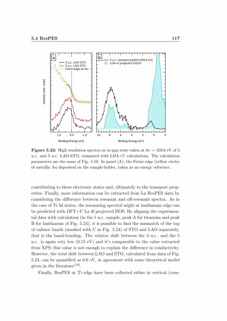
5.4 ResPES 117In
tens
ity (
arb.
uni
ts)
1.0 0.0 -1.0
Binding Energy (eV)
3 u.c. LAO-STO 5 u.c. LAO-STO Fermi edge on Au
10 8 6 4 2 0 -2
Binding Energy (eV)
5 u.c. resonant part(hν=459.6 eV) LDA+U projected d-DOS
a b
Figure 5.22: High resolution spectra on in-gap state taken at hν = 459.6 eV of 3
u.c. and 5 u.c. LAO-STO, compared with LDA+U calculations. The calculation
parameters are the same of Fig. 5.10. In panel (A), the Fermi edge (yellow circle)
of metallic Au deposited on the sample-holder, taken as an energy reference.
contributing to these electronic states and, ultimately to the transport prop-
erties. Finally, more information can be extracted from La ResPES data by
considering the difference between resonant and off-resonant spectra. As in
the case of Ti 3d states, the resonating spectral wight at lanthanum edge can
be predicted with DFT+U La 4f projected DOS. By aligning the experimen-
tal data with calculation (in the 5 u.c. sample, peak A for titanium and peak
B for lanthanum of Fig. 5.24), it is possible to find the mismatch of the top
of valence bands (marked with C in Fig. 5.24) of STO and LAO separately,
that is the band-bending. The relative shift between the 3 u.c. and the 5
u.c. is again very low (0.15 eV) and it’s comparable to the value extracted
from XPS; this value is not enough to explain the difference in conductivity.
However, the total shift between LAO and STO, calculated from data of Fig.
5.24, can be quantified as 0.6 eV, in agreement with some theoretical model
given in the literature (16).
Finally, ResPES at Ti edge have been collected either in vertical (com-

118 The LaAlO3-SrTiO3 heterostructure
Inte
nsity
(ar
b. u
nits
)
25 20 15 10 5 0
Binding Energy (eV)
850
845
840
835
830
Photon E
nergy (eV)
VBShallow Core
La M4,5 edge ResPES, 5 u.c. LAO-STOAB
C
4
2
Inte
nsity
(ar
b.un
its)
860855850845840835830
Energy
La M4,5 edge XAS, 5 u.c. LAO-STO
a
b
Figure 5.23: In panel A, ResPES data and in panel B, XAS spectrum taken at
La M4,5 edge on the 5 u.c. sample.

5.4 ResPES 119In
tens
ity (
arb.
units
)
25 20 15 10 5 0Binding Energy (eV)
Ti L2,3 Off-res (hν=450 eV) Ti L2,3 On-res (hν=458.1 eV) Resonanting part @ Ti L2,3 edge
LaM4,5 Off-res (hν=820 eV) LaM4,5 On-res (hν=836 eV) Resonanting part @ LaM4,5 edge
DFT-STO total dos DFT-LAO total dos
DFT-STO Ti d-dos DFT-LAO La f-dos
A
B
C
Figure 5.24: Comparison of ResPES at Ti L and La M edges on the 5 u.c.
sample. Top four spectra (black and red lines) are experimental data take at on
and off-resonance condition; middle (blue and green lines) spectra are the total
DOS calculated with DFT; lower spectra (yellow and grey) show the difference
of ResPES spectra as compared to DFT projected DOS. The DFT calculation
parameters are the same of Fig. 5.10.

120 The LaAlO3-SrTiO3 heterostructure
pletely in-plane) and horizontal (partly out-of-plane) linear polarized X-rays
(see Fig. 2.6); the intensity ratio of Ti3+ resonances versus the total VB spec-
tral weight is higher with the in-plane polarization geometry (see Fig. 5.25),
therefore the data shown on this section have been collected with that config-
uration. However, when subtracting the off-resonance contribution from the
on-resonance spectra, the results are virtually identical in both polarizations
(panel B of Fig. 5.25). Apart from giving the optimal experimental condition
for data collection, a polarization-dependent photoemission study can’t give
additional information concerning the physics of this system.
-1.01.0B.E.(eV)
12 8 4 0
Binding Energy (eV)
On-off resonance difference Horizontal polarization Vertical polarization
Inte
nsity
(a.
u.)
25 20 15 10 5 0
Binding Energy (eV)
hν = 495.6 eV, 5 u.c. LAO-STO Horizontal polarization Vertical polarization
a b
Figure 5.25: A comparison of ResPES spectra taken with different polarization.
In panel (a), spectra taken at maximum of Ti3+ resonance in the 5 u.c. and 3 u.c.
LAO-STO; in the inset, a detail on the in-gap level; in panel (b), the results of
difference of on-resonant and off-resonant spectra.
Summarizing, the ResPES and the XAS data suggest the following:
• There is a small but detectable Ti3+ spectral weight at Fermi level due
to a filling of empty STO d-bands, both in the insulating and in the
conductive samples. Those states are measurable only in resonance
condition;
• The Ti3+ peak has a similar shape in the two sample but differs in
intensity;
• The CIS spectra agree with the Ti3+ picture and suggest the presence
of intermixing;

5.5 AR-XPS measurements 121
• The difference in band-bending effect is virtually absent;
• A small amount of lattice distortion has to be expected as measured
by XLD.
AR-XPS measurements, presented in the next paragraph, have been car-
ried out in order to better investigate the possibility of intermixing at the
junction. Experimental results will be discussed properly in the final section
of this Chapter.
5.5 AR-XPS measurements
A cationic interdiffusion at LAO-STO junction has already been observed
by means of X-ray diffraction, as shown in Ref. (82) and (84). In short, the
experimental results usually display a reduction of the lanthanum content
in the uppermost LAO layer, a strong preferential diffusion of La ions inside
STO (Fig. 5.26) and a fractional occupancy of the interface Ti sites, although
a precise quantification of the latter cannot be done.
Given the strong angular dependence of XPS probing depth as a function
of the emission angle, an angle-resolved XPS experiment has been carried out
in order to reveal the chemical composition of each layer near the interface.
The usual XPS experimental error in element quantification is usually large,
around 10%; using a set of angular-resolved measurement it is possible to
reduce this error, although a certain knowledge of the structure has to be
known in advance. The 3 u.c. and 5 u.c. LAO-STO samples have been
analyzed by angle resolved XPS, with a non-monochromatized Al-Kα X-ray
source; the Al anode has been chosen upon Mg because of the higher photon
energy and thus because of the higher probing depth. This kind of source
is not focussed, thus the probing area is determined by the analyzer focus
dimension, which is around 1 mm; since the samples had a 5×5 mm size, XPS
signal from sample-holder hasn’t been detected even at grazing emission.
The electronic lenses of the analyzer (SCIENTA R3000 XPS/UPS/ARPES)
allowed the selection of a small angular acceptance, that has been set to
nearly ±1◦. The experimental geometry is shown in Fig. 5.27. Both the
analyzer and the source has been kept at fixed position, their relative angle
α = 55◦ being chosen to eliminate the asymmetry correction. The alignment
of the rotation stage has been checked by looking at the reflected spot of a
laser beam collimated with the analyzer nose axis.

122 The LaAlO3-SrTiO3 heterostructure
Figure 5.26: Soft X-ray diffraction results on a 5 u.c. LAO-STO sample. In
(a) the cationic occupancies and in (b) the cumulative displacement respect to
STO layer spacing. The vertical dashed line mark the ideal interface. Taken from
Ref. (82)
Figure 5.27: Experimental geometry for AR-XPS measurement. The analyzer-
to-source angle α is fixed (55◦) , the sample rotation is defined by the tilt angle
θ.
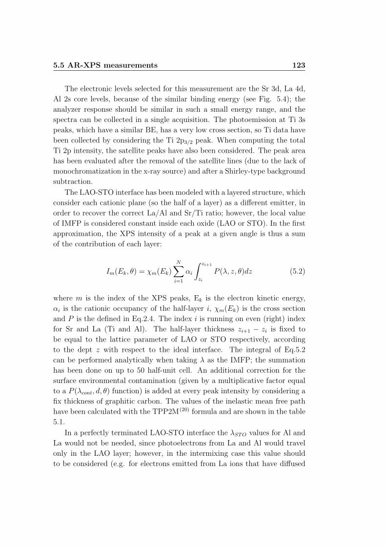
5.5 AR-XPS measurements 123
The electronic levels selected for this measurement are the Sr 3d, La 4d,
Al 2s core levels, because of the similar binding energy (see Fig. 5.4); the
analyzer response should be similar in such a small energy range, and the
spectra can be collected in a single acquisition. The photoemission at Ti 3s
peaks, which have a similar BE, has a very low cross section, so Ti data have
been collected by considering the Ti 2p3/2 peak. When computing the total
Ti 2p intensity, the satellite peaks have also been considered. The peak area
has been evaluated after the removal of the satellite lines (due to the lack of
monochromatization in the x-ray source) and after a Shirley-type background
subtraction.
The LAO-STO interface has been modeled with a layered structure, which
consider each cationic plane (so the half of a layer) as a different emitter, in
order to recover the correct La/Al and Sr/Ti ratio; however, the local value
of IMFP is considered constant inside each oxide (LAO or STO). In the first
approximation, the XPS intensity of a peak at a given angle is thus a sum
of the contribution of each layer:
Im(Ek, θ) = χm(Ek)N∑i=1
αi
∫ zi+1
zi
P (λ, z, θ)dz (5.2)
where m is the index of the XPS peaks, Ek is the electron kinetic energy,
αi is the cationic occupancy of the half-layer i, χm(Ek) is the cross section
and P is the defined in Eq.2.4. The index i is running on even (right) index
for Sr and La (Ti and Al). The half-layer thickness zi+1 − zi is fixed to
be equal to the lattice parameter of LAO or STO respectively, according
to the dept z with respect to the ideal interface. The integral of Eq.5.2
can be performed analytically when taking λ as the IMFP; the summation
has been done on up to 50 half-unit cell. An additional correction for the
surface environmental contamination (given by a multiplicative factor equal
to a P (λcont, d, θ) function) is added at every peak intensity by considering a
fix thickness of graphitic carbon. The values of the inelastic mean free path
have been calculated with the TPP2M (20) formula and are shown in the table
5.1.
In a perfectly terminated LAO-STO interface the λSTO values for Al and
La would not be needed, since photoelectrons from La and Al would travel
only in the LAO layer; however, in the intermixing case this value should
to be considered (e.g. for electrons emitted from La ions that have diffused

124 The LaAlO3-SrTiO3 heterostructure
XPS peak Ek(eV) λLAO(A) λSTO(A) λcont(A)
La 4d 1375 25.09 26.59 36.77
Sr 3d 1345 24.67 26.14 36.14
Ti 2p 1025 20.05 21.20 29.25
Al 2s 1361 24.90 26.38 36.47
Table 5.1: List of IMFP used in AR-XPS calculations, obtained by TPP-2M
formula.
deeply into the STO). The contamination correction has been added to ad-
just the angular slope of AR-XPS data; it should affect La, Sr an Al peaks in
the same way, because of the similar kinetic energy (and thus to the similar
λcont). However, since the kinetic energy of Ti 2p electrons is lower, a thick
contamination layer can reduce the intensity ratio of Ti area versus the other
elements. Finally, a common scaling factor is applied to match the experi-
mental data. The experimental results, depicted with the model results in
the case of an abrupt interface, are given in Fig. 5.28.
The peaks area is shown “as it is”, without the cross-section normaliza-
tion. The AR-XPS data clearly show the signature of X-ray photoelectron
diffraction (XPD), consistent with the data reported in literature (85); in par-
ticular, the XPD peaks at 0◦ and 45◦ can be detected, due to the forward-
scattering events that occur in a cubic lattice with this kinetic energy. This
signal modulation can increase considerably the amount of error in a fitting
procedure. In any case, the result shown in Fig. 5.28 clearly doesn’t match
the experimental results. The calculations systematically overestimate the
Ti and Sr contribution. Besides, an exchange between La and Sr ions at the
interface would even increase the discrepancy with measured data (see the
arrows in Fig. 5.28). In order to improve our model, two things have to be
done:
• On the experimental data side, it is needed to remove the photoelectron
diffraction contribution from the angular dependence of the peak area;
• On the theoretical side, it is needed to work with a better approxima-
tions for λ than the simple IMFP.
The first issue can be solved by fitting the experimental data with a

5.5 AR-XPS measurements 125
XP
S p
eaks
are
a (a
tb. u
nits
)
806040200
Tilt angle (°)
3 u.c. LAO-STO La 4d Sr 3d Ti 2p Al 2s
806040200
Tilt angle (°)
5 u.c. LAO-STO La 4d Sr 3d Ti 2p Al 2p Al 2s
Figure 5.28: Experimental AR-XPS measurement (filled circle) on the 3 u.c. and
5.u. LAO-STO, with the calculation results (thick line). The calculation has been
done on a perfectly abrupt LAO-STO configuration, with the implementation of
IMFP only. The model has been normalized to La 4d data. The arrows show the
effect of a possible La-Sr intermixing.
function that interpolates the angular dependence, averaging out the PED
effects; following Eq.2.4, this function can be expressed in this form:
f(θ) = A exp−B
cos θ (5.3)
with A and B being the parameters to be determined. The result of the data
interpolation could in principle be fitted directly with the AR-XPS model;
however, the estimated error on the A parameter is rather large as a results
of the XPD modulation on the data. To better illustrate this concept, the
experimental data on the next figures are replaced by the interpolation results
with the Eq. 5.3 with an error bar given by:
ferr(θ) = ±σA exp−B
cos θ (5.4)
where σA is the estimated error of the A parameter in the fit.
As explained in Chapter 2, the theoretical model can be improved by
replacing the IMFP with effective attenuation length (EAL), evaluated for

126 The LaAlO3-SrTiO3 heterostructure
22
21
20
19
18
17
16
E.A
.L (
Å)
200150100500
depth (Å)
Effective Attenuation LengthAl kα x-ray source
Ek = 1365 eV in LAO (Al 2s) Ek = 1380 in LAO (La 4d) Ek = 1348 eV in STO (Sr 3d) Ek = 1025 eV in STO (Ti 2p)
Figure 5.29: Calculated Effective Attenuation Length (EAL) for the measured
XPS peaks in LAO and STO. From the NIST EAL database software.
a thin overlayer geometry. Calculated EAL’s for the LAO-STO case are
shown in Fig. 5.29. Since λEAL is a function of the depth z, the integration
of Eq. 5.2 has to be done numerically. As shown in Fig. 5.29, in general
EAL increases strongly at the surface, reflecting the fact that electrons from
bulk STO should undergo to more elastic scattering events. The surface
contamination has also to be evaluated trough a different approach than the
simple graphitic layer; the carbon contamination can be estimated with an
average EAL, that can be approximated with the phenomenological formula:
λcont(Ek) = 0.0129E0.7193k (nm) (5.5)
The parameters of Eq. 5.5 have been obtained through a fitting procedure
over many measurements on different samples (86).
The results of the improved model and of the data fitting are shown
in Fig. 5.30. A 1.2 nm coverage of hydrocarbon contamination has been
estimated by fitting AR-XPS data, for both the 3 u.c. and the 5 u.c. LAO-
STO samples. A much better agreement with experimental results is found,
even without intermixing effect. In particular, the Al 2s and La 4d areas
are in good agreement with the theoretical model, while Sr and Ti peaks
are sometimes a little off the experimental error bar. These results could
be considered as a proof of the effectiveness of the EAL approach. It isn’t

5.5 AR-XPS measurements 127
possible to make a reliable structural predictions starting from the results of
Fig. 5.30. In fact, it should be noted that there’s a common multiplicative
factor; as an example of the possible mistakes, an excess of Sr can be fitted
either by increasing the Sr occupancy or by decreasing the occupancies of
all the other elements. This, together with the XPD fluctuation, does not
allow a precise fitting procedure in this case. In particular, in this case AR-
XPS can’t give a precise prediction of the depth of the intermixing, but can
anyway discriminate whether an intermixing is present.
These AR-XPS data have been used to confirm or refine the results ob-
tained with other techniques. In particular, the SXRD measurements show
a reduction of the topmost LaAlO3 layer into a reduced La(1−x)AlO3 and dis-
play a cationic intermixing occurring in the firs layer below the interface, with
the formation of a La doped STO compound. The composition proposed for
the mixed La-Sr layer in Ref. (84) can be expressed as LaxSr1−3/2x; this for-
mulation preserves the charge of a single plane, although it doesn’t describe
a complete filling of each layer. This kind of intermixing thus corresponds to
a lattice rich of cationic vacancies.
A refined solution for the 5 u.c. and 3 u.c. is given in Fig. 5.31 and in
Fig. 5.32. In both samples, the top layer has been set to a partial occupancy
x=0.8 (5 u.c.) and x=0.5 (3 u.c.), the intermixing layer has been set to a
La0.5Sr0.3. With these values, the total amount of La as compared to Al is
nearly conserved, with a reduced content of Sr on the STO termination. In
order to adjust the Ti 2p intensity, in the 5 u.c. the occupancy αTi at the
interface has to be reduced; the best fit is with αT i=0.3, but every value
below 0.6 is within the experimental error. Remarkably, in the 3 u.c. case, a
very good matching is found even without reducing the Ti occupancy at the
interface. The different Ti stoichiometry in conducting and insulating LAO-
STO can thus be reflected on the intensity of Ti3+ states as measured by
ResPES and XPS; however, further investigation would be needed to reduce
the experimental uncertainty on Ti occupation.
Finally, in Fig. 5.33 AR-XPS data taken on the insulating 5 u.c. LAO-
STO (grown with a 10−1 mBar O2 partial pressure), compared to the con-
ductive 5 u.c., are shown. With this photon energy (Al kα X-ray source), the
photoelectron diffraction peaks can be interpreted with forward-scattering
events and thus marked with the corresponding lattice direction, as shown in
Fig. 5.33. The possibility to observe the XPD modulation can be regarded
as a proof of the crystalline order of these heterostructures. Consistently

128 The LaAlO3-SrTiO3 heterostructure
0.80.40.0La
yer
Occ
upat
ion
403020100
Half-layer number (10 is the interface)
La
Sr
Ti
Al
AR
-XP
S In
tens
ity (
arb.
uni
ts) Exp. data 5 u.c.
Theory (no intermixing) Exp. error bar
La 4d Sr 3d
403020100
Half-layer number (6 is the interface)
La
Sr
Ti
Al
AR
-XP
S In
tens
ity (
arb.
uni
ts)
806040200
Tilt angle (°)
Ti 2p Al 2s
806040200
Tilt angle(°)
Ti 2p Al 2s
Exp. data 3 u.c. Theory (no intermixing)
Exp. error bar
La 4d Sr 3d
Figure 5.30: Experimental AR-XPS measurement (filled circle) on the 3 u.c.
and 5.u. LAO-STO, fitted with Eq. 5.3, with the calculation results (thick line).
The confidence bands on the experimental data fitting are also shown. For the
sake of clarity, the spectra for the perovskite A and B cations are displayed in
different graphs. These calculations have been done on a perfectly abrupt LAO-
STO configurations, with the introduction of the EAL. The layer occupation for
each case is shown in the lower panel.
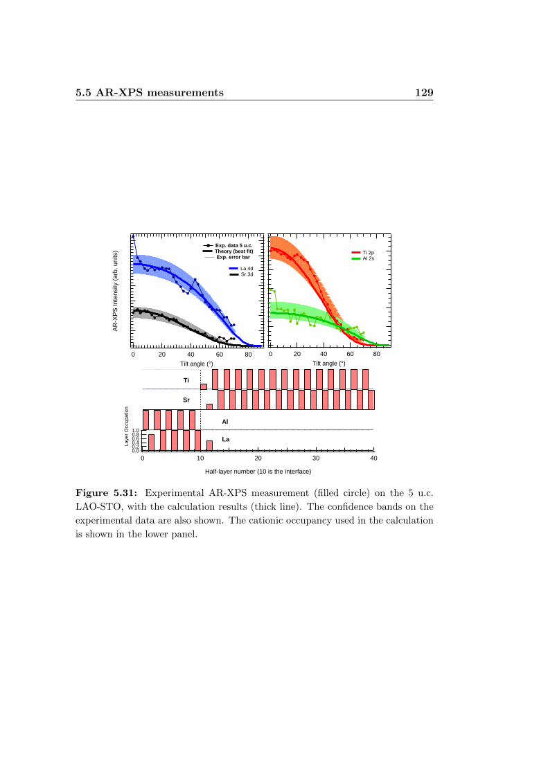
5.5 AR-XPS measurements 129
806040200
Tilt angle (°)
Ti 2p Al 2s
AR
-XP
S In
tens
ity (
arb.
uni
ts)
806040200
Tilt angle (°)
Exp. data 5 u.c. Theory (best fit) Exp. error bar
La 4d Sr 3d
1.00.80.60.40.20.0
Laye
r O
ccup
atio
n
403020100
Half-layer number (10 is the interface)
La
Sr
Ti
Al
Figure 5.31: Experimental AR-XPS measurement (filled circle) on the 5 u.c.
LAO-STO, with the calculation results (thick line). The confidence bands on the
experimental data are also shown. The cationic occupancy used in the calculation
is shown in the lower panel.

130 The LaAlO3-SrTiO3 heterostructure
AR
-XP
S in
tens
ity (
arb.
uni
ts)
806040200Tilt angle(°)
Exp. data 3 u.c. Theory (intermixing)
Exp. error bar (due to XPD)
La 4d Sr 3d
1.00.80.60.40.20.0
Laye
r O
ccup
atio
n
403020100
Half-layer number (6 is the interface)
La
Sr
Ti
Al
806040200Tilt angle(°)
Ti 2p Al 2s
Figure 5.32: Experimental AR-XPS measurement (filled circle) on the 3 u.c.
LAO-STO, with the calculation results (thick line). The confidence bands on the
experimental data are also shown. The cationic occupancy used in the calculation
is shown in the lower panel. Note that the Ti occupancy at the interface layer is
full.

5.5 AR-XPS measurements 131
Pea
k A
rea
(arb
. uni
ts)
80706050403020100
Tilt angle (°)
[001]
[101]
[103]
[102]
[201]
[301]
Insulating 5ML
La 4d Sr 3d Ti 2p Al 2s
Conductive 5ML
La 4d Sr 3d Ti 2p Al 2s
Figure 5.33: AR-XPS data taken on conductive and insulating 5 u.c. samples.
The lattice directions associated to the XPD forward scattering process are also
shown. Data of the two samples are normalized to match the La 4d AR-XPS
spectra.
with results shown in Fig. 5.4, the Al 2s peak intensity is weaker in the in-
sulating sample than in the conductive one, because of the different growth
regime. By comparing the intensities of each cationic species, it seems that
the insulating 5 u.c. sample is thus aluminium poor rather than lanthanum
rich. The LAO-STO samples grown in 10−1 mBar (or higher) O2 pressure
thus can’t be compared with the ones grown at lower partial pressure, which
also displays the physical properties of interest.
Summarizing the AR-XPS results, a clear signature of La intermixing in
the bulk STO is found in both the 3 u.c. and 5 u.c. samples, in a similar way.
A good data matching can be found following the structural model extracted
from SXRD measurements, which should be accompanied by a reduction of
Ti at the interface in the 5 u.c. case. In any case, since an abrupt model does
not match exactly with the experimental data, every physical description of
the conductivity in the LAO-STO heterostructures should account for an
amount of disorder at the interface.

132 The LaAlO3-SrTiO3 heterostructure
5.6 Conclusions
The most interesting signatures of the conductivity shown in this Chapter
are the in-gap states detected with ResPES at the Ti L2,3 edge. We provided
the first experimental evidence (17) of these states, probed with soft X-rays
spectroscopies. Following our investigation, a similar ResPES analysis has
been carried out by A. Koitzsch et al. (87) on LAO-STO interfaces grown
with different oxygen partial pressure. They reported the presence of in-gap
states, especially in their “oxygen poor” sample. Also in this case the oxygen
stoichiometry seems to play a crucial role to determine the presence of Ti
3d1 electronic levels .
In our samples, the different spectral weight of in-gap states seem to be
directly related to the interface conductivity. Surprisingly, the Ti3+ states
have also been clearly observed in the insulating sample, with the same peak
shape and at the same energy of the conductive one. In a common metal, the
rise of conductivity should be marked by an increasing DOS at Fermi level,
as measured in LAO-STO, induced by a shift of the Fermi-level, which has
not be observed in this case. The XPS binding energies are almost the same
in insulating and conductive LAO-STO. The presence of VO due to X-ray
damages should be excluded, since the X-ray penetration depth is much larger
than the LAO capping and thus a similar amount of X-ray defects should has
been detected in each sample. Moreover, the photoemission spectra did not
change upon the exposition to the synchrotron X-ray beam over the entire
period of the data acquisition (nearly 5 days).
As a starting point we should consider that both samples are correlated
systems, with a much higher effective mass in the “insulating” sample; in that
case, however, a different quasiparticle peak-shape at Fermi level should be
observed, as can be seen in 3d1 correlated metals (for example, in V2O3(88))
and in theoretical models (for example, the Dynamical Mean Field The-
ory (89)). Moreover, as shown with DFT+U DOS calculations, the in-gap
states can be described with a simple band-filling of the empty STO lev-
els (83).
Since the difference in the Ti3+ states of 3 and 5 u.c. samples is only
a scaling factor without a detectable energy shift, the conductivity may be
related to a phase separation mechanism which, in turn, is driven by the
thickness of the LAO layer. In any case, the problem is to find a suitable
“doping” mechanism that can justify the presence of these conductive Ti3+

5.6 Conclusions 133
Figure 5.34: Doping versus temperature phase diagram of SrTiO3/LaAlO3 in-
terfaces. The doping scale consists of three possible contributions: intrinsic carrier
doping from the electronic reconstruction (xint), carrier doping from oxygen vacan-
cies (xO2 ) and carrier doping by applied electric fields (xfield). Observed transport
effects are insulation at p-type interfaces (77)(x¡0), 2D interface metallicity (77), 3D
bulk metallicity (77), negative magneto resistance (90) below 70 K, magnetic hys-
teresis (90) below 300 mK, and superconductivity (78) below Tc=200 mK. The ex-
act position of xint in the phase diagram is not yet known and can vary due to
other polarity discontinuity compensating mechanisms (such as xO2 ).Taken from
Ref. (11).
states at the LAO-STO interfaces.
The different conductivity mechanism found in the literature have been
summarized (11) by M. Hujiben et al. in the phase diagram of Fig. 5.34. Three
different type of doping are underlined: the intrinsic doping (xint), related to
the electronic reconstruction, the extrinsic doping (xO2 , mostly due to VO)
and the external electric field (xfield). It should be noted that an electrical-
field driven transition from the superconductive to the metallic state has
been reported (91), thus justifying the presence of the xfield parameter in Fig.
5.34. The 3D metallic phase correspond to a high density of VO, due to
the low PO2 during the growth. The superconductivity has been observed
for an intermediate PO2 regime , while in the optimal regime the localized
magnetic moments have been detected. The sample analyzed in this thesis
work belong to the latter group. The value of xint in Fig. 5.34 is still
unknown; in particular, it cannot be put in the intermediate region because
oxygen vacancies can have a non negligible role in the superconductivity.
The observed in-gap states could be ascribed for instance to a cationic dis-

134 The LaAlO3-SrTiO3 heterostructure
order at the interface; in fact, STO can became conductive even for small La
doping. In order to justify the 4 u.c. thickness threshold, the disorder should
be dependent to the number of LAO capping layer; however, the cationic
interdiffusion seems to be similar in conductive and insulating samples, as
shown in section 5.5 and in the literature by N. Nakagawa et al. (92).
The metallic areas can also be generated by the presence of residual oxy-
gen vacancies near the interface; as in the case of TiO2−δ, an oxygen vacancy
could create localized defect states, that above certain concentrations can
merge to yield a metallic band. In a recent article (93), Z. Zhong and co-
workers report DFT calculations suggesting that the formation energy of
oxygen vacancies in LAO-STO interfaces is thickness dependent. However,
our samples should also display the presence of isolated magnetic moments
that in turn cannot be provided by isolated oxygen vacancies alone, similarly
to the TiO2−δ case of Chapter 4. The magnetism could appear only in the
case of clustered defects at the interface (11). The possibility to reduce the
influence of VO by mean of the growth conditions and the sharp thickness
threshold suggest that interface VO can play a minor role in the conductivity,
at least in our samples.
Finally, in the electronic reconstruction scenario the relaxation of the
polar discontinuity is achieved by a 1/2 e− charge-transfer from the surface
to the interface, which in fact should result in the presence of reduced Ti3.5+
in the uppermost STO layer (77). A practical implementation of this concept
is the band-bending effect (94), which has never been observed in these systems
by means of X-ray spectroscopies (15). Moreover, ab-initio calculations carried
out on a LAO-STO interface with different types of cationic disorder (15) show
that the intermixing can be thermodynamically favorable and can reduce the
LAO polarity effects.
Another kind of electronic reconstruction is a ferroelectric-like distortion
of the first LAO layer at the interface. As expected, the average c cell pa-
rameter in the capping LAO (3.79 A) is usually lower than the STO planar
distance (82) (3.89 A); however, SXRD and HRTEM (95) measurements show
that the first unit cell at the interface is elongated by 4%-9% (up to 4.1 A).
This elongation is explained by the authors with the presence of Ti3+ ions
at the interface (thus with a larger ionic radius with respect to Ti4+), in
a sort of Jahn-Teller effect. A structural deformation due to the strain in
LAO capping that is spread also in STO has also been reported in a recent
investigation with high-resolution XRD (96). As already pointed out in Sec-

5.6 Conclusions 135
tion 5.3, the distortion of the oxygen octahedral cage around the interface
Ti atoms has already been measured with XLD (81) and in a similar way in
our samples. Surprisingly, Ti3+ electronic levels cannot be observed by XAS,
and XLD results can be explained completely with Ti4+ CT-multiplet calcu-
lation only. However, CIS spectra clearly agrees with a Ti3+ picture of the
conductive Ti 3d states. In any case, in the electronic reconstruction frame
the presence of the Ti3+ states at Fermi edge in insulating LAO-STO cannot
be explained, at least without assuming an inhomogeneous distribution of
the distorted sublattice at the interface.
Another interesting theory that could fit our experimental results has
been proposed by N. C. Bristowe and co-workers (16); by recognizing that
most of the measurement on this oxides have been done at atmospheric pres-
sure (or, as in this case, with an environmental atmosphere surface contam-
ination), the doping at the LAO-STO interface could be given by a surface
contamination or surface defects.
The relaxation of the polar discontinuity can thus be achieved by the same
charge-transfer process of the electronic reconstruction model, but without
the need of a band bending, which should also imply a conductive surface. In
this model, the oxygen reduction at the surface should create a potential well
for the induced localized charge in the 3d-level at the interface; in the authors
view, the localization radius would be inversely proportional to the depth of
the well, i.e. to the LAO thickness: hence the reason of the conductivity. A
pictorial representation is given in Fig.5.35.
This model can also explain a peculiar effect that has been reported on
insulating LAO-STO interface. In fact, Y. Xie et al. (97) have shown that it
is possible to draw (and erase) conductive lines on LAO-STO by moving a
biased AFM tip on the LAO surface. The authors suggest that the driving
mechanism of this process is the creation of defects at the surface; in the
surface-reduction model, the biased tip just raises (or decreases, according
to the bias sign) the vacancy stability. Recently published ab-initio DFT cal-
culations of the VO formation energies in the LAO-STO further support this
description (98). A possible way to check the influence of the surface reduction
on the LAO-STO conductivity could be to use LAO-STO junction as a “gas
sensor”; it should be possible to measure a variable sample resistance upon
the exposition to different gases or to directly measure the Ti-3d spectral
weight with the aid of ResPES in a synchrotron facility.
In conclusion, the LAO-STO system displays a wealth of physical and

136 The LaAlO3-SrTiO3 heterostructure
Figure 5.35: Schematic view of the thickness dependence on interface electrons
localization from the model of Ref. (16). Trapping potential V created by a surface
O vacancy as seen by interface electrons versus distance within the interface plane
x (x=0 is directly below the vacancy) for film thickness d=a (deepest), 2a, 3a,
4a (shallowest), with harmonic estimates of corresponding donor ground states
[taking meff = 3me]. Inset: Sketch of range and density of trapped states.
chemical properties, which challenge both theoretical and experimental physi-
cist. A single interface “doping” source is not enough to explain the various
phenomena that occur at this interface. In fact, the theoretical models that
involve perfectly abrupt interfaces and clean surfaces cannot completely ex-
plain the different experimental evidences. In this scenario, surface effects
and electronic phase separation are thought to play a major role, so far often
disregarded.

Bibliography
[1] P. A. Cox. Transition Metal Oxides. Clarendon Press - Oxford, 1992.
[2] V. E. Henrich and P. A. Cox. The Surface Science of Metal Oxides.
Cambridge University Press, 1994.
[3] N. Tsuda, K. Nasu, A. Yanase, and K. Siratori. Electronic Conduction
in Oxides. Springer-Verlag, 1991.
[4] U. Diebold. Surf. Sci. Rep., 48:53, 2003.
[5] J. M. D. Coey, M. Venkatesan, and C. B. Fitzgerald. Nat. Mat., 4:173,
2005.
[6] J. Coey, P. Stamenov, R. D. Gunning, M. Venkatesan, and K. Paul.
New. J. of Phys., 12:053025, 2010.
[7] M. Venkatesan, C. B. Fitzgerald, and J. M. D. Coey. Nature (London),
430:630, 2004.
[8] M. Khalid, A. Setzer, M. Ziese, P. Esquinazi, D. Spemann, A. Poppl,
and E. Goering. Phys. Rev. B., 81:214414, 2010.
[9] J. M. D. Coey and S. A. Chambers. MRS Bull., 33:1053, 2008.
[10] S. Thiel, G. Hammerl, A. Schmehl, C. W. Schneider, and J. Mannhart.
Science, 313:1942, 2006.
[11] Mark Huijben, Alexander Brinkman, Gertjan Koster, Guus Rijnders,
Hans Hilgenkamp, and D. H. A. Blank. Adv. Mat., 21:1665–1667, 2009.
[12] J.F. Schooley, W.R. Hosler, E. Ambler, J.H. Becker, M.L. Cohen, and
C.S. Koonce. Phys. Rev. Lett., 14:305, 1965.

138 BIBLIOGRAPHY
[13] A. D. Caviglia, S. Gariglio, C. Cancellieri, B. Sacepe, A. Fete, N. Reyren,
M. Gabay, A. F. Morpurgo, and J.-M. Triscone. Phys. Rev. Lett.,
105:236802, 2010.
[14] R. Pentcheva and W. E. Pickett. J. Phys.: Cond. Mat., 22:043001, 2010.
[15] S. A. Chambersa, M. H. Engelhard, V. Shutthanandan, Z. Zhua, T.C.
Droubaya, L. Qiao, P.V. Sushkob, T. Fengc, H.D. Lee, T. Gustafsson,
E. Garfunkel, A.B. Shahd, J. M. Zuod, and Q. M. Ramassee. Surf. Sci.
Rep., 65:317–352, 2010.
[16] N. C. Bristowe, P. B. Littlewood, and E. Artacho. Phys. Rev. B,
83:205405, 2011.
[17] G. Drera, F. Banfi, F. Federici Canova, P. Borghetti, L. Sangaletti,
F. Bondino, E. Magnano, J. Huijben, M. Huijben, G. Rijnders, D. H. A.
Blank, H. Hilgenkamp, and A. Brinkman. App. Phys. Lett, 98:052907,
2011.
[18] F. De Groot and A. Kotani. Core level spectroscopy of solids. CRC
Press, 2008.
[19] J.J. Yeh and I.Lindau. Atomic Data and Nuclear Data Tables, 32:1–155,
1985.
[20] S. Tanuma, C. J. Powell, and D. R. Penn. J. Elec. Spec, 62:95, 1993.
[21] S. Tougaard. J. Vc. Sci and Tech. A, 14:1415, 1996.
[22] A. Jablonsky and C. J. Powell. Surf. Sci. Rep., 47:33, 2002.
[23] Cedric Powell. Nist electron effective-attenuation-length database. www.
nist.gov/srd/nist82.cfm.
[24] B. H. Frazer, B. Gilbert, B. R. Sonderegger, and G. De Stasio. Surf.
Sci., 537:161–167, 2003.
[25] R. C. Albers J. J. Rehr. Rev. Mod. Phys., 72:621, 2000.
[26] G. Drera, M.C. Mozzati, P. Galinetto, Y. Diaz-Fernandez, L. Malavasi,
F. Bondino, M. Malvestuto, and L.Sangaletti. Appl. Phys. Lett.,
97:012506, 2010.

BIBLIOGRAPHY 139
[27] R. D. Cowan. The Theory of Atomic Structure and Spectra. Los Alamos
Series in Basic and Applied Sciences, 1981.
[28] R. Gusmeroli. www.esrf.eu/computing/scientific/MISSING/.
[29] L. Sangaletti, G. Drera, E. Magnano, F. Bondino, C. Cepek, A. Sepe,
and A. Goldoni. Phys. Rev. B., 81:085204, 2010.
[30] S. Doniach and M. Sunjic. J. Phys., 4C31:285, 1970.
[31] P. A. Bruhwiler, O. Karis, and N. Martennson. Rev. Mod. Phys., 74:703,
2002.
[32] N. Martennson, M. Weinelt, O. Karis, M. Magnuson, N. Wassdahl,
A. Nilsson, J. Stohr, and M. Samant. Appl. Phys A, 65:159, 1997.
[33] U. Fano. Phys. Rev., 124:1866, 1961.
[34] L. Sangaletti, A.Verdini, S. Pagliara, G. Drera, L. Floreano, A. Goldoni,
and A. Morgante. Phys. Rev. B., 81:245320, 2010.
[35] R. M. Martin. Electronic Structure. Basic Theory and Practical Methods.
Cambridge University Press, 2004.
[36] A. Szabo and N. S. Ostlund. Modern Quantum Chemistry: Introduction
to Advanced Electronic Structure Theory. McGraw-Hill, 1989.
[37] R. M. Dreizler and E. K. U. Gross. Density Functional Theory. Springer-
Verlag, 1990.
[38] D.M. Ceperley and B. J. Alder. Phys. Rev. Lett., 45:566, 1980.
[39] J. P. Perdew, K. Burke, and M. Ernzerhof. Phys. Rev. Lett., 77:3865,
1996.
[40] X. Gonze, B. Amadon, P.-M. Anglade, J.-M. Beuken, F. Bottin,
P. Boulanger, F. Bruneval, D. Caliste, R. Caracas, M. Cote, T. Deutsch,
L. Genovese, Ph. Ghosez, M. Giantomassi, S. Goedecker, D.R. Hamann,
P. Hermet, F. Jollet, G. Jomard, S. Leroux, M. Mancini, S. Mazevet,
M.J.T. Oliveira, G. Onida, Y. Pouillon, T. Rangel, G.-M. Rignanese,
D. Sangalli, R. Shaltaf, M. Torrent, M.J. Verstraete, G. Zerah, and
J.W. Zwanziger. Comp. Phys. Commun., 180:2582–2615, 2009.

140 BIBLIOGRAPHY
[41] M. C. Payne, M. P. Teter, D. C. Ailan, T. A. Arias, and J. D.
Joannopouios. Rev. Mod. Phys., 64:1045, 1992.
[42] E. Anglada, J. M. Soler, J. Junquera, and E. Artacho. Phys. Rev. B,
66:205101, 2002.
[43] M. Cococcioni and S. Gironcoli. Phys. Rev. B, 71:035105, 2005.
[44] A. E. Bocquet, T. Mizokawa, K. Morikawa, A. Fujimori, S. R. Bar-
man, K. Maiti, D. D. Sarma, Y. Tokura, and M. Onoda. Phys. Rev. B,
53:1161, 1996.
[45] A. Tanaka and T. Jo. J. Phys. Soc. Jpn., 63:2788, 1994.
[46] K. C. Prince and V.R. Dhanak. Phys. Rev. B, 55:9520, 1997.
[47] A. G. Thomas and W.R. Flavell. Phys. Rev. B, 75:035105, 2007.
[48] P. Le Fevre, J. Danger, and H. Magnam. Phys. Rev. B, 69:155421, 2004.
[49] K. Okada and A. Kotani. J. Elec. Spec. Rel. Phen., 62:131, 1993.
[50] P. Kruger. J. of Phys.: Conf. Series, 190:012006, 2009.
[51] M. Torrent, F. Jollet, F. Bottin, and X. Gonze. Comp. Mat. Sci., 42:337–
351, 2008.
[52] E. Cho, S. Han, H.S. Ahn, K.R. Lee, S. K. Kim, and C. S. Hwang. Phys.
Rev. B, 73:193202, 2006.
[53] Seong-Geon Park, Blanka Magyari-Kope, , and Yoshio Nishi. Phys. Rev.
B, 82:115109, 2010.
[54] G. Drera, L. Malavasi, Y. Diaz-Fernandez, F. Bondino, M. Malvestuto,
M.C. Mozzati, P. Galinetto, and L. Sangaletti. Origin, excitation dy-
namics, and symmetry of the insulating TiO2−δ electronic states probed
by resonant photoelectron spectroscopies at the Ti L-edge. submitted
to Phy. Rev. Lett, 2011.
[55] T. Saha-Dasgupta, A. Lichtenstein, M. Hoinkis, S. Glawion, M. Sing,
R. Claessen, and R. Valentı. New J. Phys., 9:380, 2007.

BIBLIOGRAPHY 141
[56] S. Hufner, S. H. Yang, B. S. Mun, C. S. Fadley, J. Schafer, E. Rotenberg,
and S. D. Kevan. Phys. Rev. B, 61:12582, 2000.
[57] R. Ruus, A. Saar, J. Aark, A. Aidla, T. Uustare, and A. Kikas. J. Elec.
Spec. Rel. Phen., 93:193, 1998.
[58] T. Dietl, H. Ohno, F. Matsukura, J. Cibert, and D. Ferrand. Science,
287:1019, 2000.
[59] T. Fukumura, Z. Jin, M. Kawasaki, T. Shono, T. Hasegawa, S. Koshi-
hara, and H. Koinuma. Appl. Phys. Lett., 78:958, 2001.
[60] Y. Matsumoto, M. Murakami, T. Shono, T. Hasegawa, T. Fukumura,
M. Kawasaki, P. Ahmet, T. Chikyow, S.Y. Koshihara, and H. Koinuma.
Science, 291:854, 2001.
[61] Y. Matsumoto, M. Murakami, T. Hasegawa, T. Fukumura,
M. Kawasaki, P. Ahmet, K. Nakajima, T. Chikyow, S.Y. Koshihara,
and H. Koinuma. Appl. Surf. Sci., 189:344, 2002.
[62] Y. Soo, G. Kioseoglou, S. Kim, Y. Kao, P. S. Devi, J. Parise, R. Gam-
bino, and P. Gouma. Appl. Phys. Lett., 81:655, 2002.
[63] W. Park, R. Ortega-Hertogs, J. Moodera, A. Punnoose, and M. Seehra.
J. Appl. Phys., 91:655, 2002.
[64] M. C. Mozzati, P. Galinetto, C. B. Azzoni, L.Sangaletti, A. Speghini,
and M. Bettinelli. J. Phys.:Cond. Mat., 18:7643, 2006.
[65] Nguyen Hoa Hong, Joe Sakai, Ngo Thu Huong, Nathalie Poirot, and
Antoine Ruyter. Phys. Rev. B, 72:045336, 2005.
[66] K. Ueda, H. Tabata, and T. Kawai. Appl. Phys. Lett., 79:988–990, 2001.
[67] J. Osorio-Guillen, S. Lany, S.V. Barabash, and A. Zunger. Phys. Rev.
Lett., 96:107203, 2006.
[68] M. H. Henderson. Surf. Sci, 419:174, 1999.
[69] G. V. Samsonov. The Oxide Handbook. IFI/Plenum Press, 1982.

142 BIBLIOGRAPHY
[70] I. S. Elfimov, A. Rusydi, S. I. Csiszar, Z. Hu, H. H. Hsieh, H.-J. Lin,
C. T. Chen, R. Liang, and G. A. Sawatzky. Phys. Rev. Lett., 98:137202,
2007.
[71] F. Rossella, P. Galinetto, M. C. Mozzati, L. Malavasi, Y. Diaz Fernan-
dez, G. Drera, and L. Sangaletti. J. Raman Spec., 41:558–565, 2010.
[72] S. Oseroff and P. H. Keesom. Semiconductors and Semimetals, vol-
ume 25. Academic,New York, 1988.
[73] L. Sangaletti, C. Mozzati, G. Drera, V. Aguekian, L. Floreano, and
A. Morgante. Appl. Phys. Lett., 96:142105, 2010.
[74] J. Osorio-Guillen, S. Lany, S.V. Barabash, and A. Zunger. Phys. Rev.
B, 75:184421, 2007.
[75] E. Martinez-Ferrero, Y. Sakatani, C. Boissiere, D. Grosso, A. Fuertes,
J. Fraxedas, and C. Sanchez. Adv. Func. Mater., 17:33483354, 2001.
[76] S. H. Cheung, P. Nachimuthu, A. G. Joly, M. H. Engelhard, M. K.
Bowman, and S. A. Chambers. Surf. Sci, 601:1754, 2007.
[77] A. Ohtomo and H. Y. Hwang. Nature, 427:423, 2004.
[78] N. Reyren, S. Thiel, A. D. Caviglia, L. Fitting Kourkoutis, G. Hammerl,
C. Richter, C. W. Schneider, T. Kopp, A. S. Ruetschi, D. Jaccard,
M. Gabay, D. A. Muller, J. M. Triscone, and J. Mannhart. Science,
317:1196, 2007.
[79] G. Rijnders and D. H. A. Blank. Nat. Mat., 7:270, 2008.
[80] M. Sing, G. Berner, K. Goß, A. Muller, A. Ruff, A. Wetscherek, S. Thiel,
J. Mannhart, S. A. Pauli, C. W. Schneider, P. R. Willmott, M. Gorgoi,
F. Schafers, and R. Claessen. Phys. Rev. Lett., 102:176805, 2009.
[81] M. Salluzzo, J. C. Cezar, N. B. Brookes, V. Bisogni, G. M. De Luca,
C. Richter, S. Thiel, J. Mannhart, M. Huijben, A. Brinkman, G. Rijn-
ders, and G. Ghiringhelli. Phys. Rev. Lett., 102:166804, 2009.
[82] P. R. Willmott, S. A. Pauli, R. Herger, C. M. Schleputz, D. Martoc-
cia, B. D. Patterson, B. Delley, R. Clarke, D. Kumah, C. Cionca, and
Y. Yacoby. Phys. Rev. Lett., 99:155502, 2007.

BIBLIOGRAPHY 143
[83] Yukiaki Ishida, Ritsuko Eguchi, Masaharu Matsunami, Koji Horiba,
Munetaka Taguchi, Ashish Chainani, Yasunori Senba, Haruhiko Ohashi,
Hiromichi Ohta, and Shik Shin. Phys. Rev. Lett., 100:056401, 2008.
[84] V. Vonk, J. Huijben, D. Kukuruznyak, A. Stierle, H. Hilgenkamp,
A. Brinkman, and S. Harkema. A-site Vacancies at SrTiO3/LaAlO3
Interfaces uncovered by Anomalous Surface X-ray Diffraction. To be
published, 2011.
[85] M. El Kazzi, C. Merckling, G. Delhaye, L. Arzel, G. Grenet, E. Bergig-
nat, and G. Hollinger. Mat. Sci. Semicond. Proc., 9:954–958, 2006.
[86] Graham C. Smith. J. El. Spec. Rel. Phen., 148:21–28, 2005.
[87] A. Koitzsch, J. Ocker, M. Knupfer, M. C. Dekker, K. Dorr, B. Buchner,
and P. Hoffmann. Phys. Rev. B, 84:245121, 2011.
[88] S.-K. Mo, J. D. Denlinger, H.-D. Kim, J.-H. Park, J. W. Allen,
A. Sekiyama, A. Yamasaki, K. Kadono, S. Suga, Y. Saitoh, T. Muro,
P. Metcalf, G. Keller, K. Held, V. Eyert, V. I. Anisimov, and D. Voll-
hardt. Phys. Rev. Lett., 90:186403, 2003.
[89] Antoine Georges, Gabriel Kotliar, Werner Krauth, and Marcelo J.
Rozenberg. Rev. Mod. Phys., 68:13–125, 1996.
[90] A. Brinkman, M. Huijben, M. Van Zalk, J. Huijben, U. Zeitler,
J. C. Maan, W. G. Van der Wiel, G. Rijnders, D. H. A. Blank, and
H. Hilgenkamp. Nat. Mat., 6:493, 2007.
[91] A. D. Caviglia, S. Gariglio, N. Reyren, D. Jaccard, T. Schneider,
M. Gabay, S. Thiel, G. Hammerl, J. Mannhart, and J.M. Triscone. Na-
ture, 456:624, 2008.
[92] D. A. Muller N. Nakagawa, H. Y. Hwang. Nat. Mat., 5:204, 2006.
[93] Zhicheng Zhong, P. X. Xu, and Paul J. Kelly. Phys. Rev. B, 82:165127,
2010.
[94] Rossitza Pentcheva and Warren E. Pickett. Phys. Rev. Lett., 102:107602,
2009.

144 BIBLIOGRAPHY
[95] J.L. Maurice, I. Devos, M.J. Casanove, C. Carretero, G. Gachet, G. Her-
ranz, D.G. Crete, D. Imhoff, A. Barthelemy, M. Bibes, K. Bouzehouane,
C. Deranlot, S. Fusil, E. Jacquet, B. Domenges, and D. Ballutaud. Mat.
Sci. Eng. B, 1:144, 2007.
[96] J. E. Boschker, C. Folkman, C. W. Bark, A. F. Monsen, E. Folven,
J. K. Grepstad, E. Wahlstrom, C. B. Eom, and T. Tybell. Phys. Rev.
B, 84:205418, 2011.
[97] Yanwu Xie, Christopher Bell, Takeaki Yajima, Yasuyuki Hikita, and
Harold Y. Hwang. Nano Lett., 7:2588–2591, 2010.
[98] Yun Li, Sutassana Na Phattalung, Sukit Limpijumnong, Jiyeon Kim,
and Jaejun Yu. Phys. Rev. B, 84:245307, 2011.