understanding noise in the signal chain webinar
TRANSCRIPT

Understanding Noise in the Signal Chain
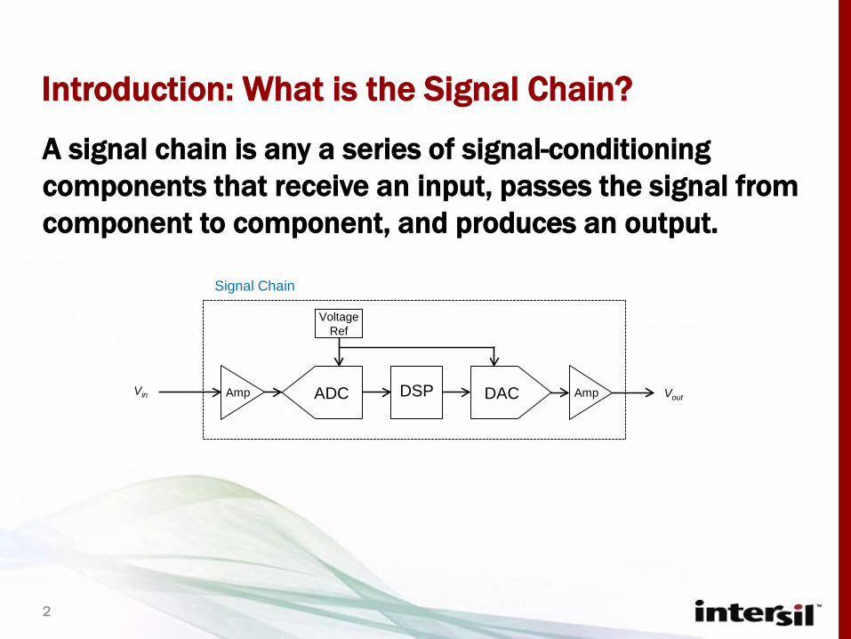
Introduction: What is the Signal Chain?
A signal chain is any a series of signal-conditioning components that receive an input, passes the signal from component to component, and produces an output.
ADC DSP DACVin Vout
Signal Chain
Voltage Ref
Amp Amp
2

• Our focus is on the internal sources of noise– Noise in semiconductor devices in general– Noise in data converters in particular
• Noise is any electrical phenomenon that is unwelcomed in the signal chain
Introduction: What is Noise?
ADC DSP DAC+ +
Ideal Signal Path, Gain (G)
VextExternal Noise
VintInternal Noise
Vin G·(Vin + Vext) + Vint
Signal Chain
Voltage Ref
Amp Amp
3

Noise in Semiconductor Devices
1. How noise is specifieda. Noise amplitudeb. Noise spectral density
2. Types of noisea. White noise sourcesb. Pink noise sources
3. Reading noise specificationsa. Time domain specsb. Frequency domain specs
4. Estimating noise amplitudesa. Creating a noise spectral density plotb. Finding the noise amplitude
4

Noise in Semiconductor Devices
1. How noise is specifieda. Noise amplitudeb. Noise spectral density
2. Types of noisea. White noise sourcesb. Pink noise sources
3. Reading noise specificationsa. Time domain specsb. Frequency domain specs
4. Estimating noise amplitudesa. Creating a noise spectral density plotb. Finding the noise amplitude
5

Noise in Semiconductor DevicesHow Noise is Specified: Amplitude
Semiconductor noise results from random processes and thus the instantaneousamplitude is unpredictable. Amplitude exhibits a Gaussian (Normal) distribution.
The ratio of is called the Cresting Factor
Noise Amplitude
rmspp VnVn ⋅= 6.6
rms
pp
VV
Root Mean Square (RMS)
Peak-to-Peak (PP)
t
+σ-σ
+2σ
-2σ
-3σ
+3σ
+4σ
-4σ
Noise Voltage Density
VnPP
VnRMS
μ
+3.3σ
-3.3σ
6

2=RMS
P
VV
2=RMS
P
VV
2=RMS
P
VV
3=RMS
P
VV
1=RMS
P
VV
6.6=RMS
PP
VV
Noise in Semiconductor DevicesHow Noise is Specified: AmplitudeCommon Cresting Factors
7
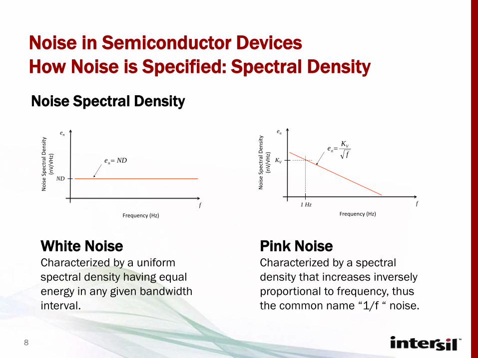
Noise in Semiconductor DevicesHow Noise is Specified: Spectral Density
White NoiseCharacterized by a uniform spectral density having equal energy in any given bandwidth interval.
Pink Noise Characterized by a spectral density that increases inversely proportional to frequency, thus the common name “1/f “ noise.
en
ND
Noi
se S
pect
ral D
ensit
y (n
V/√H
z)
Frequency (Hz)
f
NDen=
en
KV
Noi
se S
pect
ral D
ensit
y (n
V/√H
z)
Frequency (Hz)
f
fKe V
n=
1 Hz
Noise Spectral Density
8
Semiconductor noise is a combination of white and pink noise, resulting in the noise spectral density curve shown below, plotted on a log-log scale.
en
Fc
ND
Noi
se S
pect
ral D
ensit
y (n
V/√H
z)
Frequency (Hz)Fl
f
1+
=
fFcNDen
Fh
Noise in Semiconductor DevicesHow Noise is Specified: Spectral Density
9

Noise in Semiconductor DevicesHow Noise is Specified: Spectral DensitySemiconductor noise is a combination of white and pink noise, resulting in the noise spectral density curve shown below, plotted on a log-log scale.
en
Fc
ND
Noi
se S
pect
ral D
ensit
y (n
V/√H
z)
Frequency (Hz)Fl
f
1+
=
fFcNDen
Fh
Corner frequency, Fc, is where Pink noise density equals White noise density
ND is the White Noise Density
10

Noise in Semiconductor Devices
1. How noise is specifieda. Noise amplitudeb. Noise spectral density
2. Types of noisea. White noise sourcesb. Pink noise sources
3. Reading noise specificationsa. Time domain specsb. Frequency domain specs
4. Estimating noise amplitudesa. Creating a noise spectral density plotb. Finding the noise amplitude
11

• Uniform spectral density having equal energy in any given bandwidth
• Distinctive appearance on an oscilloscope
(1us/div)
en
NDN
oise
Spe
ctra
l Den
sity
(nV/
√Hz)
Frequency (Hz)
f
NDen=
Noise in Semiconductor DevicesTypes of Noise: White NoiseWhite Noise
12
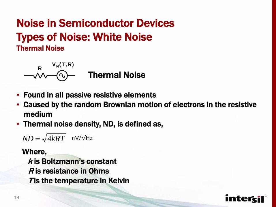
• Found in all passive resistive elements• Caused by the random Brownian motion of electrons in the resistive
medium• Thermal noise density, ND, is defined as,
kRTND 4=
Where,k is Boltzmann’s constantR is resistance in Ohms T is the temperature in Kelvin
Thermal Noise
nV/√Hz
Noise in Semiconductor DevicesTypes of Noise: White NoiseThermal Noise
RVN(T,R)
13

• Generated whenever charge crosses a potential barrier • Caused by the fact that current flowing cross a junction is not
smooth, but is made of individual electrons arriving at random times
• Shot noise density, ND, is defined as,
qIND 2=
Where,q is the electric chargeI is the current flowing through the barrier
Shot Noise
nA/√Hz
Noise in Semiconductor DevicesTypes of Noise: White NoiseShot Noise
14

• Found in PN junctions operating in reverse breakdown mode, such as Zener diodes
• Caused by carriers developing sufficient energy to dislodge additional carriers through physical impact – resulting in a fluctuation in current
• Like shot noise, avalanche noise requires the flow of current
Avalanche Noise
nA/√Hz ( )IfND =
Noise in Semiconductor DevicesTypes of Noise: White NoiseAvalanche Noise
I
IN(I)
15

Noise in Semiconductor DevicesTypes of Noise: Pink Noise
• Spectral density increases with decreasing frequency. It contains equal amounts of voltage in each decade of bandwidth
• Distinctive appearance on an oscilloscope
(1s/div, 0.1 to 10Hz BW)
en
KV
Noi
se S
pect
ral D
ensit
y (n
V/√H
z)
Frequency (Hz)
f
fKe V
n=
1 Hz
Pink Noise
16

• Found in all types of transistors and some types of resistors. Always associated with DC current
• Caused by random fluctuations in current due to contamination in semiconductor materials
• Flicker noise density, ND, is defined as,
f
KIND 1=
Where,K is a device constantI is the DC currentf is the frequency (1s/div, 0.1 to 10Hz BW)
Flicker Noise (1/f Noise)
nA/√Hz
Noise in Semiconductor DevicesTypes of Noise: Pink NoiseFlicker Noise
I
17
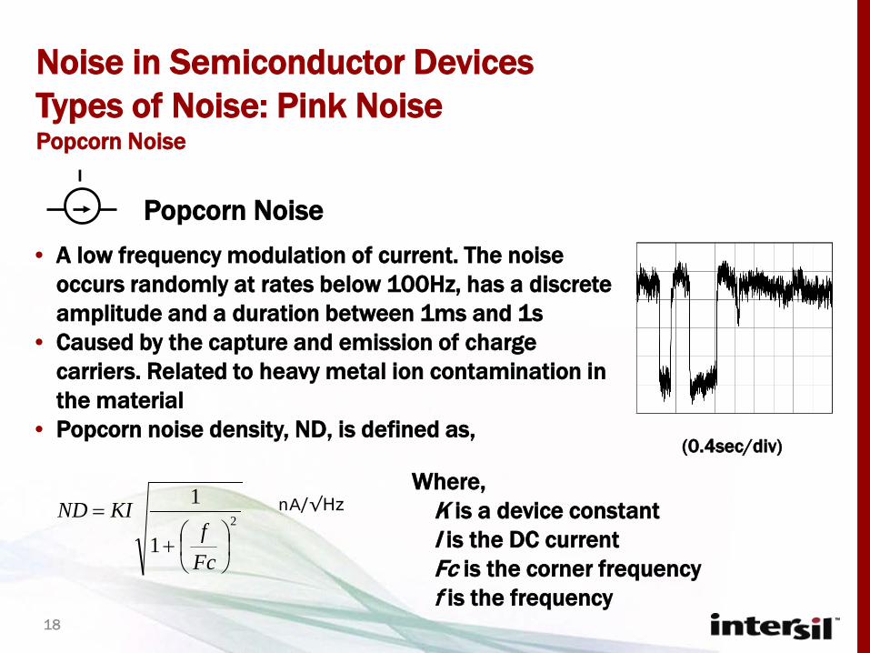
• A low frequency modulation of current. The noise occurs randomly at rates below 100Hz, has a discrete amplitude and a duration between 1ms and 1s
• Caused by the capture and emission of charge carriers. Related to heavy metal ion contamination in the material
• Popcorn noise density, ND, is defined as,
2
1
1
+
=
Fcf
KINDWhere,
K is a device constant I is the DC current Fc is the corner frequency f is the frequency
(0.4sec/div)
Popcorn Noise
nA/√Hz
Noise in Semiconductor DevicesTypes of Noise: Pink NoisePopcorn Noise
I
18

Noise in Semiconductor DevicesTypes of Noise: kT/C
kT/C noise is not a fundamental noise source, but is thermal noise in the presence of a filter capacitor. The R terms drops out leaving Vn = kT/C.
kT/C Noise
en
Noi
se S
pect
ral D
ensit
y (n
V/√H
z)
Frequency (Hz)
fRC
f dB π21
3 =
kRTen 4=
Increases with R
Decreases with R
19

Noise in Semiconductor Devices
1. How noise is specifieda. Noise amplitudeb. Noise spectral density
2. Types of noisea. White noise sourcesb. Pink noise sources
3. Reading noise specificationsa. Time domain specsb. Frequency domain specs
4. Estimating noise amplitudesa. Creating a noise spectral density plotb. Finding the noise amplitude
20

Noise in Semiconductor DevicesReading Noise Specifications
DACsADCs VRefs Amplifiers
• Electrical Specifications Table
• Typical Performance Curves Section
21

Noise in Semiconductor DevicesReading Noise SpecificationsTime Domain Specifications
Noise Voltage AmplitudeISL21090 Voltage Reference – ES Table
• Peak to Peak, µVP-P6.2µVpp is the “flicker” or “1/f” noise. It can be identified as flicker noise by the low frequency band (0.1Hz to 10Hz) in the conditions column
• Root Mean Square, µVRMSIt is measured over a wider and higher frequency band of 10Hz to 1kHz, where white noise dominates, and 1/f noise is negligible
22
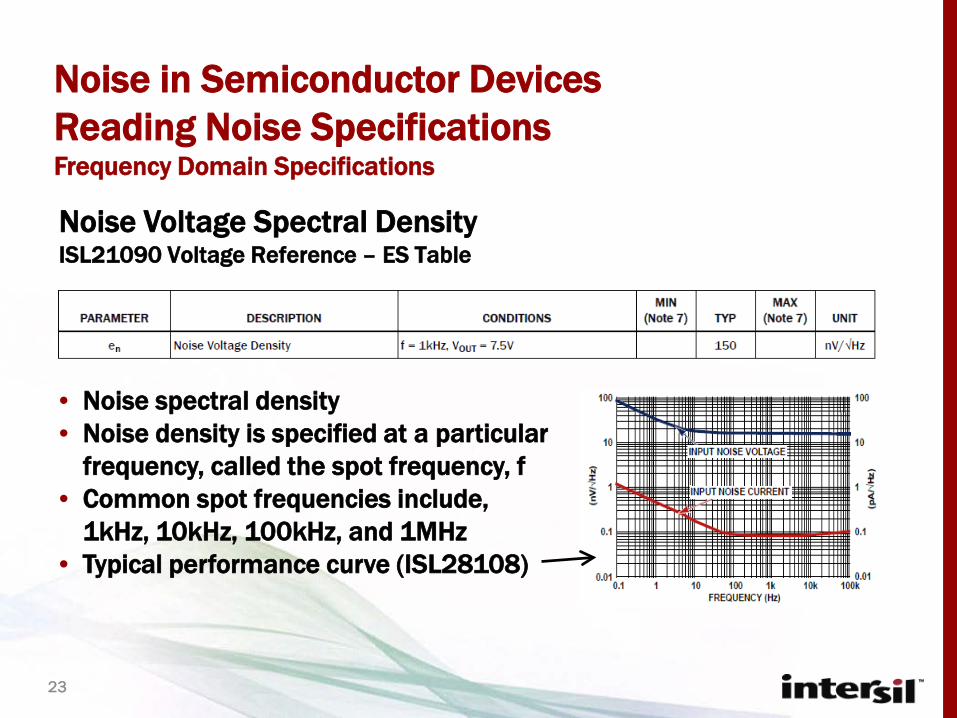
Noise in Semiconductor DevicesReading Noise SpecificationsFrequency Domain Specifications
Noise Voltage Spectral DensityISL21090 Voltage Reference – ES Table
• Noise spectral density• Noise density is specified at a particular
frequency, called the spot frequency, f• Common spot frequencies include,
1kHz, 10kHz, 100kHz, and 1MHz• Typical performance curve (ISL28108)
23

1. How noise is specifieda. Noise amplitudeb. Noise spectral density
2. Types of noisea. White noise sourcesb. Pink noise sources
3. Reading noise specificationsa. Time domain specsb. Frequency domain specs
4. Estimating noise amplitudesa. Creating a noise spectral density plotb. Calculating the noise
Noise in Semiconductor Devices
24

Noise in Semiconductor DevicesEstimating Noise AmplitudesHere is the key …
The noise voltage present over any bandwidth is the Root Sum Square (RSS) of the area under the noise spectral density curve, between the upper (Fh) and lower (Fl) frequencies of the band.
25

Noise in Semiconductor DevicesEstimating Noise Amplitudes
FlFhFlFhFcNDdf
fFcNDVn
Fh
Flrms −+
⋅=
+
= ∫ ln1
2/12
The noise voltage can be predicted over any desired frequency band if the noise spectral density (ND) and corner frequency (Fc) are known.
Simplifying,
26

Noise in Semiconductor DevicesEstimating Noise AmplitudesThermal Noise Calculator
Uses the equations,
All variables can be entered or found
FlFhFlFhFcNDVnrms −+
⋅= ln
rmspp VnVn ⋅= 6.6
)15.273(4 += TkRND
A calculator for making quick work of noise calculations
27

Noise in Semiconductor DevicesEstimating Noise AmplitudesThermal Noise Calculator
28
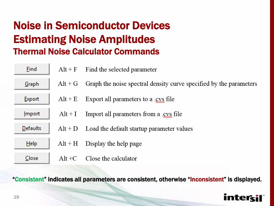
Noise in Semiconductor DevicesEstimating Noise AmplitudesThermal Noise Calculator Commands
“Consistent” indicates all parameters are consistent, otherwise “Inconsistent” is displayed.
29

Noise in Semiconductor DevicesEstimating Noise AmplitudesTypically, datasheets only provide three noise specs in the EP table
1. Noise density (ND) 2. Flicker noise (Vnpp)3. Wideband noise (Vnrms)
30

Noise in Semiconductor DevicesEstimating Noise AmplitudesExample – Customer Question
What is the output noise voltage (Vn) of the ISL21090 voltage reference over the audio band of 20Hz to 20kHz?
We will use the calculator and datasheet to find the answer. We will draw the noise spectral density curve to help us visualize what the calculator is doing.
ISL21090-7.5V
Vn
31
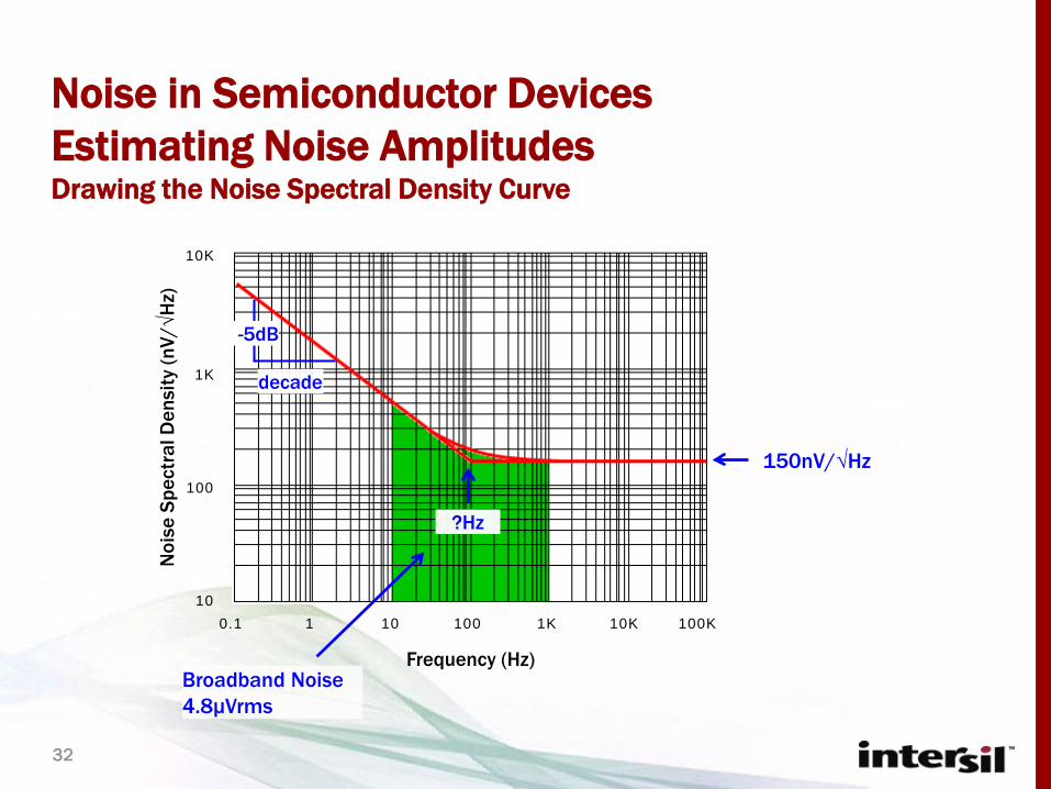
Noise in Semiconductor DevicesEstimating Noise AmplitudesDrawing the Noise Spectral Density Curve
0.1 1 10 100 1K 10K 100K
100
1K
10
10K
Noi
se S
pect
ral D
ensi
ty (n
V/√H
z)
Frequency (Hz)
?Hz
decade
-5dB
150nV/√Hz
Broadband Noise4.8μVrms
32
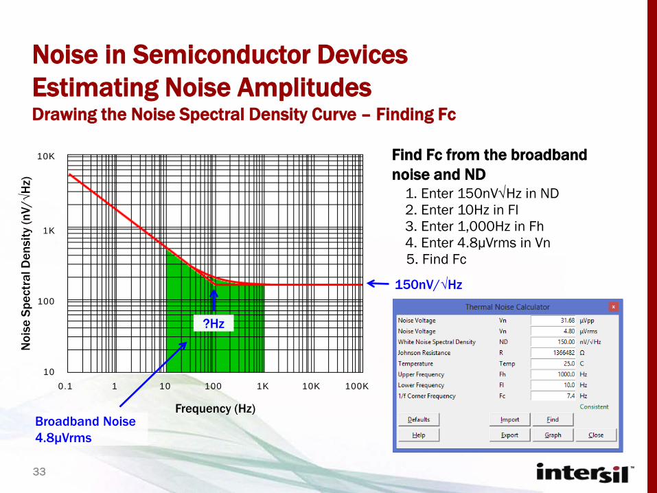
Noise in Semiconductor DevicesEstimating Noise AmplitudesDrawing the Noise Spectral Density Curve – Finding Fc
0.1 1 10 100 1K 10K 100K
100
1K
10
10K
Noi
se S
pect
ral D
ensi
ty (n
V/√H
z)
Frequency (Hz)
?Hz
150nV/√Hz
Broadband Noise4.8μVrms
2. Enter 10Hz in Fl1. Enter 150nV√Hz in ND
3. Enter 1,000Hz in Fh4. Enter 4.8µVrms in Vn5. Find Fc
Find Fc from the broadband noise and ND
33
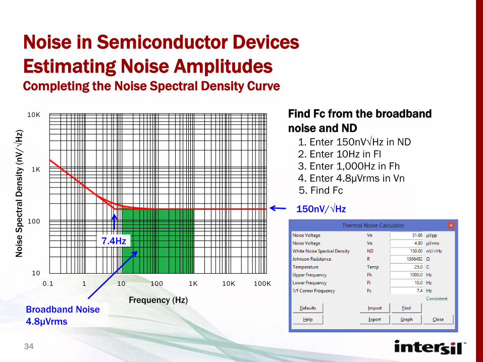
Noise in Semiconductor DevicesEstimating Noise AmplitudesCompleting the Noise Spectral Density Curve
2. Enter 10Hz in Fl1. Enter 150nV√Hz in ND
3. Enter 1,000Hz in Fh4. Enter 4.8µVrms in Vn5. Find Fc
Find Fc from the broadband noise and ND
0.1 1 10 100 1K 10K 100K
100
1K
10
10K
Noi
se S
pect
ral D
ensi
ty (n
V/√H
z)
Frequency (Hz)
7.4Hz
150nV/√Hz
Broadband Noise4.8μVrms
34

Noise in Semiconductor DevicesEstimating Noise AmplitudesEstimating the Output Noise Voltage Over the Full Audio Band
0.1 1 10 100 1K 10K 100K
100
1K
10
10K
Noi
se S
pect
ral D
ensi
ty (n
V/√H
z)
Frequency (Hz)
Find the audio band noise, noise not given in the datasheet:
Audio Band Noise21.2µVrms
1. Enter 20Hz in Fl2. Enter 20,000Hz in Fh3. Enter Vn
35

Noise in Semiconductor DevicesEstimating Noise AmplitudesVerifying the 1/f Noise
100
1K
10
10K
Noi
se S
pect
ral D
ensi
ty (n
V/√H
z)
0.1 1 10 100 1K 10K 100K10
Frequency (Hz)
Check the 1/f noise with the datasheet
1/f Noise
Calculated: 6.6 µVppDatasheet: 6.2 µVpp
36
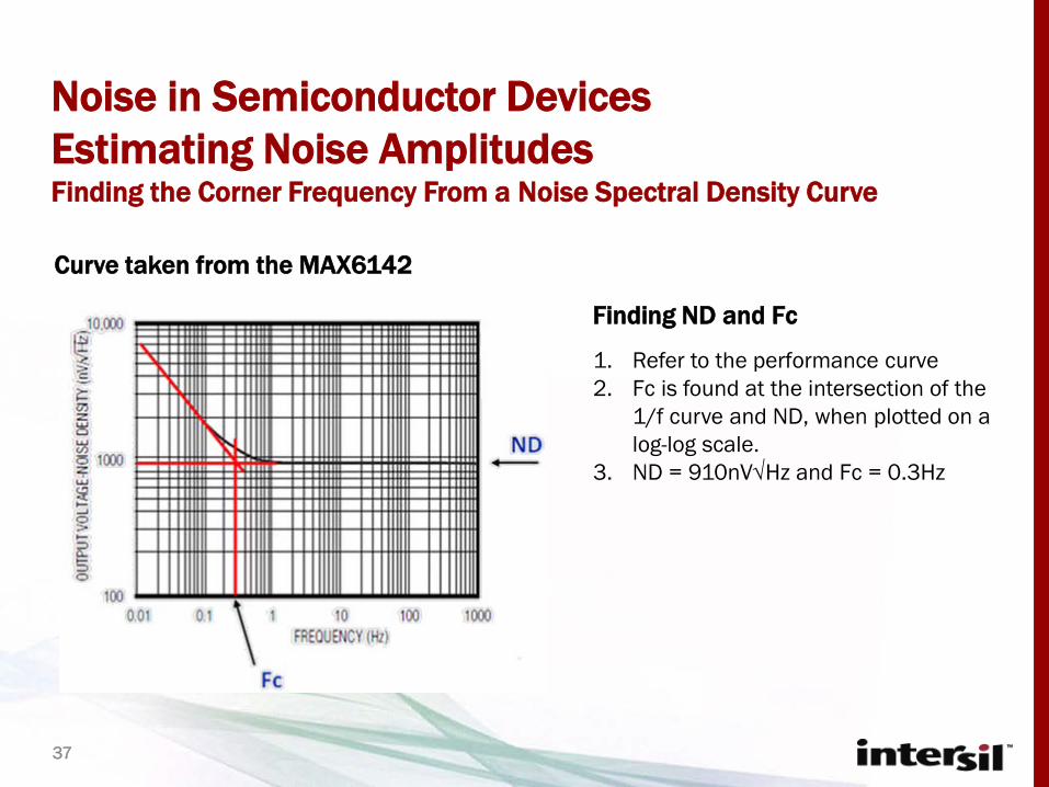
Noise in Semiconductor DevicesEstimating Noise AmplitudesFinding the Corner Frequency From a Noise Spectral Density Curve
1. Refer to the performance curve 2. Fc is found at the intersection of the
1/f curve and ND, when plotted on a log-log scale.
3. ND = 910nV√Hz and Fc = 0.3Hz
Finding ND and Fc
Curve taken from the MAX6142
37

Noise in Semiconductor DevicesEstimating Noise AmplitudesEstimating the Output Noise Voltage Over the Full Audio Band
4. Enter 20,000Hz in Fh3. Enter 20Hz in Fl
5. Find Vn: 128.6µVrms20Hz 20kHz
128.6µVrms
2. Enter 0.3Hz in Fc1. Enter 910nV√Hz in ND
0.3Hz
910nV√Hz
38

Noise in Semiconductor DevicesEstimating Noise AmplitudesComponent Selection Example
Example – Customer RequirementAn audio application requires a Signal to Noise Ratio (SNR) of 105dB with a 5Vpp audio signal. This represents a noise budget of 10μVrms. Assuming the DAC noise is negligible, determine if the output noise of the ISL21090-5V meets our noise budget over the audio band of 20Hz to 20kHz.
Vn ≤ 10μVrms ?
Digital InputAnalog Output
Sample Clock
DAC
ISL21090-5VVoltage
Reference
ISL21090-5V Vn
39

Noise in Semiconductor DevicesHow Noise is Specified: Noise AmplitudeAdding Random Noise Sources
All uncorrelated noise sources sum geometrically, in Root Sum Square (RSS) fashion.
223
22
21 ... nnnnnnT eeeee ++++=
• One term often dominates RMS sums. For example,
If enREF = 300nV√Hz and enDAC = 100nV√Hz then enT = 316nV√Hz
The DAC only contributes 16nV/√Hz!
• When fighting uncorrelated noise - focus on the dominant term
22nDACnREFnT eee +=
40

Noise in Semiconductor DevicesEstimating Noise AmplitudesDrawing the Noise Spectral Density Curve for the ISL21090-5V
0.1 1 10 100 1K 10K 100K
100
1K
10
10K
Noi
se S
pect
ral D
ensi
ty (n
V/√H
z)
Frequency (Hz)
50nV/√Hz
7.4Hz
41

Noise in Semiconductor DevicesEstimating Noise AmplitudesEstimating the Output Noise Voltage Over the Full Audio Band
0.1 1 10 100 1K 10K 100K
100
1K
10
10K
Noi
se S
pect
ral D
ensi
ty (n
V/√H
z)
Frequency (Hz)
Find the audio band noise - noise not given in the datasheet:
Audio Band Noise 7.08µVrms
42

Noise in Semiconductor DevicesEstimating Noise AmplitudesFinding the Maximum Allowable Bandwidth
0.1 1 10 100 1K 10K 100K
100
1K
10
10K
Noi
se S
pect
ral D
ensi
ty (n
V/√H
z)
Frequency (Hz)
Find the maximum allowable bandwidth for the noise budget:
Audio Band Noise10µVrms
39.9kHz
43
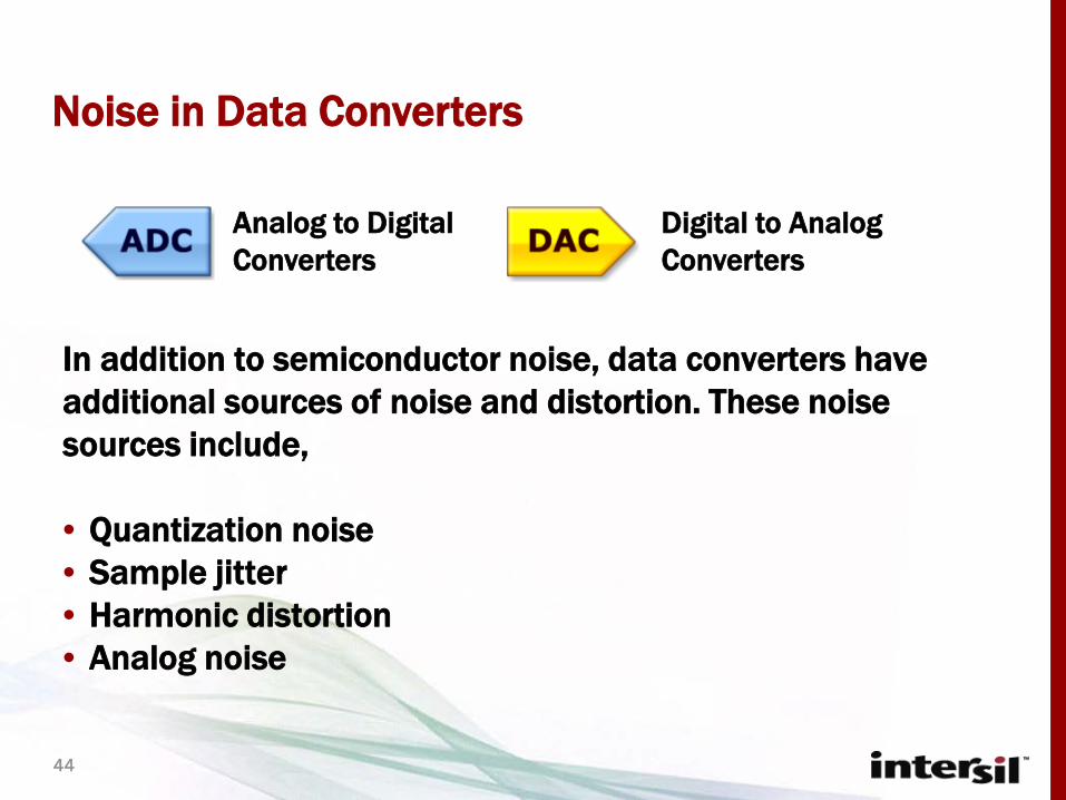
Noise in Data Converters
In addition to semiconductor noise, data converters have additional sources of noise and distortion. These noise sources include,
• Quantization noise• Sample jitter • Harmonic distortion • Analog noise
Analog to Digital Converters
Digital to AnalogConverters
44

Noise in Data Converters
• Noise Sources– Quantization noise– Sample jitter– Harmonic distortion– Analog noise
• How noise is specified in data converters
• Selecting the best data converter for a given noise budget
45

Noise can be redistributed among sources within a signal chain as long as the total noise budget is not exceeded.
•Additional external noise sources are shown in red.• Improvements can be made by using a lower noise and
distortion input amplifier (ADC) or external driver (DAC), lower noise voltage reference, or a lower jitter sample clock.
NDigital Output
ENOB, SINAD, DNL, THD
ADCAnalog Input, THD, VN
ΦJ
TJTHD, VN
VoltageReference
VN
VN
Noise in Data ConvertersNoise Sources Exist in the Signal Chain and Data Converters
46

• Noise Sources– Quantization noise
• Resolution• Differential nonlinearity• Bandwidth
– Sample jitter– Harmonic distortion– Analog noise
• How noise is specified in data converters
• Selecting the best data converter for a given noise budget
Noise in Data Converters
47

Noise in Data ConvertersQuantization Noise - Resolution, N
Increasing resolution (N) means decreasing quantization noise (nqPP)
Digital Output
Analog Input
Quantization Error
SignalLSBnqPP ⋅=1
Digital Output
Analog Input
Quantization Error
Signal
LSBnqPP ⋅=1
N bit resolution N+1 bit resolution
Least Significant Bit (LSB): 1 LSB = , where FS is the full scale valueNFS2
48
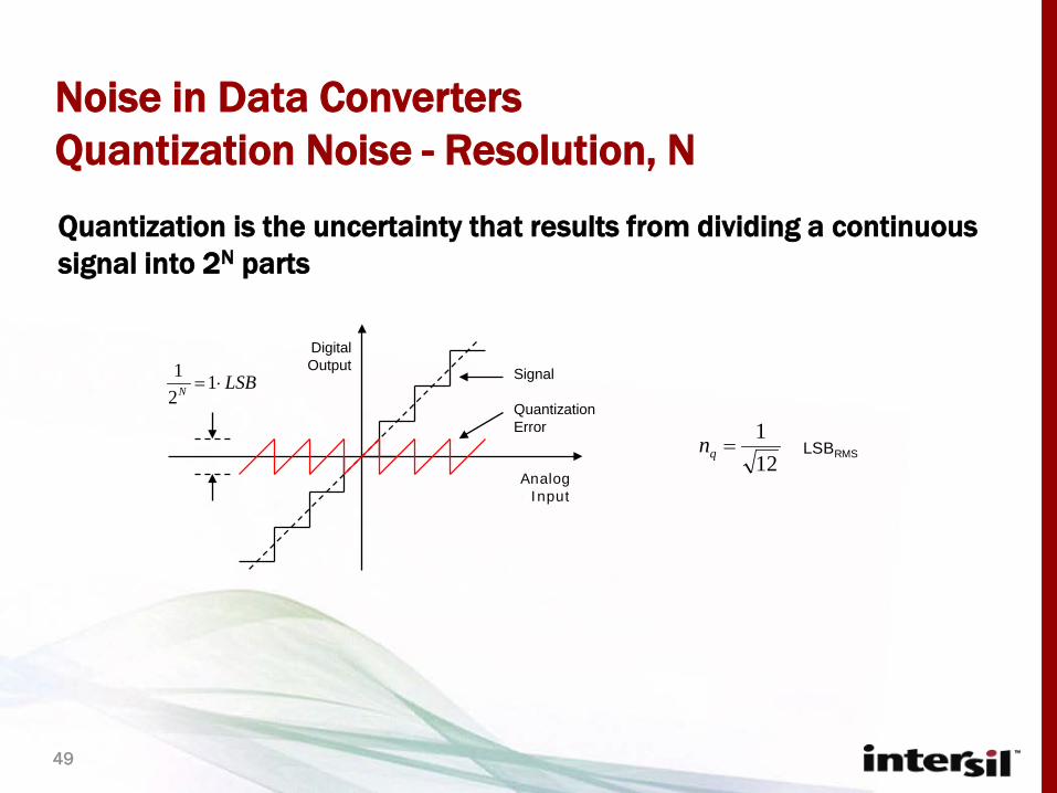
Noise in Data ConvertersQuantization Noise - Resolution, N
Quantization is the uncertainty that results from dividing a continuous signal into 2N parts
121
=qn LSBRMS
DigitalOutput
Quantization Error
SignalLSBN ⋅=121
Analog Input
49

Noise in Data ConvertersQuantization Noise - Differential Nonlinearity, DNLDifferential Nonlinearity (DNL) is the deviation of any code width from an ideal 1LSB step. An ideal data converter has a DNL of 0.
The average DNL of a data converter increases its average quantization error and therefore its quantization noise.
121 DNLnq+
= LSBRMS
DigitalOutput
Analog Input
Quantization Error
Signal
+
NDNL2
1
50

Noise in Data ConvertersQuantization Noise - Bandwidth, BWThe quantization noise described up to this point are over the full Nyquistbandwidth (BW).
• Decreasing BW decreases noise
• If the sample frequency (Fs) and the input signal are harmonically uncorrelated then the noise is Gaussian and is distributed evenly between DC and Fn
• BW is defined here as a percentage of FN, %
LSBRMS
Quantization Noise
BW FN
212)1(
FsDNL+
Noise Density
Freq0 FS
( )
12
1100
DNLBW
nq
+=
51

Noise in Data ConvertersQuantization Noise - Oversample Rate, OSR
Alternatively, Over Sample Ratio (OSR) can be used in place of BW.
• OSR is the ratio of some higher sample rate OSR⋅Fs to the original Fs, sampling the full original Nyquist bandwidth. Increasing OSR decreases noise.
• Oversampling is used in Sigma-Delta converters to reduce noise.
LSBRMS
Quantization NoiseBW
FN
212)1(
OSRFsDNL+
Noise Density
FreqFS OSR·FS0
( )
12
11 DNLOSRnq
+=
52

Noise in Data Converters
• Noise sources– Quantization noise
• Resolution• Differential nonlinearity• Bandwidth
– Sample jitter– Harmonic distortion– Analog noise
• How Noise is specified in data converters
• Selecting the best data converter for a given noise budget
53

Noise in Data ConvertersSample Jitter, TjSample jitter introduces noise when sampling a time varying signal, by producing unwanted variations in sampled values.
Input Sine wave
Time
Clock Jitter Noise
Sample Clock Clock Jitter, tJitter
Input Period, tIn
Input Sine wave
Time
Clock Jitter Noise
Sample Clock Clock Jitter, tJitter
Input Period, tIn LSBRMSN
In
Jitterj t
tn 28
2⋅⋅=
π
FS
0
Internal source: Sample and Hold (SAH) aperture jitter
External source: Sample clock phase jitter
54

Noise in Data ConvertersHarmonic DistortionHarmonic distortion is a distortion of a signal caused by the presence of unwanted harmonics
• Nonlinearities within a channel is a common cause of harmonic distortion
55

VCC
-+
RL
VDAC VOUT
VEE
VCC
RL
VDAC
VOUT
VEE
Noise in Data ConvertersHarmonic DistortionHarmonic Distortion in Drivers
VOH
VEE
VCC
0
VEE VCC0
VOL
Linear Range
Output Range
V OUT
VDAC
Saturation Region
Saturation Region
56

Noise in Data ConvertersTotal Harmonic Distortion, THDTotal Harmonic Distortion (THD) is a standard measure of harmonic distortion
Noise levels due to THD are related by
++++⋅=
FSVVVVVV
THD2
52
42
32
22
1log20
∑ ==
5
12
n nTHD Vn
THD is defined as the ratio of the RMS sum of the first five harmonics to the full scale RMS signal amplitude (VFS)
The total noise contributed by harmonic distortion is the RSS sum of all harmonic components
10082 %THDn
N
THD ⋅=
20108
2 dBTHDN
THDn ⋅=
LSBRMS
LSBRMS
When THD is given in % of the FS RMS signal
When THD is given in dB of the FS RMS signal
57

Noise in Data ConvertersTotal Harmonic Distortion, THDExample Harmonic Distortion - Showing the 2nd and 3rd harmonic
58

Noise in Data ConvertersHarmonic DistortionSpurious Free Dynamic Range (SFDR)SFDR is the ratio of the amplitude of the fundamental frequency to the amplitude of the largest magnitude of harmonic or spurious signal component observed over the full bandwidth.
59

IMD is the result of two or more signals of different frequencies being mixed together, forming additional signals. Inter-modulation is caused by the nonlinear behavior of the signal processing being used.
3A-2
B2A
-B
3B-2
A
2B2A FrequencyA B
TypicalChannel
Bandwidth
2B-A
3A 3B
2nd orderIMD
B-A
3rd orderIMD
5th orderIMD
3rd orderIMD
5th orderIMD
3rd
Harmonics
2nd
Harmonics
Amplitude
Noise in Data ConvertersHarmonic DistortionInter-modulation Distortion (IMD)
60

Noise in Data ConvertersGlitch EnergyGlitches are short spikes in voltage at the output of a DAC. The “energy” of the glitch is expressed in units of nanovolt-seconds (nV⋅s).
0
V OUT
Bipolar glitch due to capacitive coupling
t0
V OUT
Unipolar glitch due to switching skews
t
Area G2Area G1 Glitch Area
Glitch Area = G2- G1
61

Noise in Data ConvertersAnalog Noise, VnAnalog Noise (Vn) is the effective noise referred to the input of an ADC or the output of a DAC
It is the RMS sum of all semiconductor noise sources referred to the analog side of a data converter
IdealDAC +
Vn
Analog Output
IdealADC+
Vn
Analog Input
IdealDAC +
Vn
Analog Output
IdealDAC +
Vn
Analog Output
IdealADC+
Vn
Analog Input
IdealADC+
Vn
Analog Input
VnnAN =
VnnAN ⋅= 6.6
LSBRMS
LSBPP
62

• Noise sources– Quantization noise
• Resolution• Differential nonlinearity• Bandwidth
– Sample jitter– Harmonic distortion– Analog noise
• How noise is specified in data converters
• Selecting the best data converter for a given noise budget
Noise in Data Converters
63

Noise in Data ConvertersHow Noise is Specified In Data ConvertersISL26712 ADC
Typical Performance Characteristics Plot
Average DNL ≈ 0.3LSB
64

Noise in Data ConvertersHow Noise is Specified in Data Converters
- MAX5170 DAC
- MAX1062 ADC
65

Noise in Data Converters
• Noise sources– Quantization noise
• Resolution• Differential nonlinearity• Bandwidth
– Sample jitter– Harmonic distortion– Analog noise
• How noise is specified in data converters
• Selecting the best data converter for a given noise budget
66

Noise in Data ConvertersSelecting the Best Data Converter For Your Noise Budget
A noise budget is the allocation of noise within a signal chain that results in an acceptable SNR at the output.
• SNR is the RMS signal level to the total RMS noise.
Therefore, the method used to determine the acceptable distribution of noise within a signal chain is to evaluate their effect on total SNR.
• Two new specifications used in data converters will be introduced.– Signal to Noise and Distortion (SINAD)– Effective Number of Bits (ENOB)
⋅=
RMS
RMS
VnVsSNR log20 dB
What is a noise budget?
67

Noise in Data ConvertersSelecting the Best Data ConverterSignal to Noise and Distortion, SINAD
Pulling it all together…
Data converters combine these noise sources into one parameter called Signal to Noise and Distortion (SINAD)
Quantization Noise Sample Jitter Noise
Analog Noise
THD
( ) 2%
22
6
2
100222
102
2
1100
32log20
+
⋅⋅+
+
+
−=THDVnTjDNLBW
SINAD NN π dB
Where,N is the resolution, in bitsDNL is the average differential nonlinearity, in LSBBW is the fraction of the full Nyquist bandwidth used, in percentTj is the ratio of the RMS jitter of the sample period to the period of a sine wave, in PPMVn is the analog noise, in LSBRMSTHD is the total harmonic distortion, in percentage
68

Noise in Data ConvertersSelecting the Best Data ConverterSignal to Noise and Distortion, SINAD
SINAD reduces to the familiar, rule-of-thumb, equation
Together, these parameter values describe the “ideal” data converter.
dBNSNR 76.102.6 += dB
When,DNL = 0LSBTj = 0PPMVn = 0LSBTHD = 0%BW = 100%
69

Noise in Data ConvertersSelecting the Best Data ConverterEffective Number of Bits, ENOBEffective Number of Bits (ENOB) is a data converter’s effective resolution from an SNR perspective.
• ENOB is an AC specification and is synonymous with Signal to Noise and Distortion (SINAD). They are related by the equation,
• ENOB says that a data converter has a level of noise and distortion equivalent to an ideal (i.e., noise and distortion free) data converter of ENOB over the full bandwidth.
( )2202310
Log
LogSINADENOB
⋅
⋅−
= bit
70

Noise in Data ConvertersSelecting the Best Data ConverterENOB Calculator
• All variable can be entered or found
• Uses the equations,
Quantization Noise Sample Jitter Noise
Analog Noise
THD
( ) 2%
22
6
2
100222
102
2
1100
32log20
+
⋅⋅+
+
+
−=THDVnTjDNLBW
SINAD NN π
( )2202310
Log
LogSINADENOB
⋅
⋅−
=
A calculator for making quick work of noise calculations in data converters
71
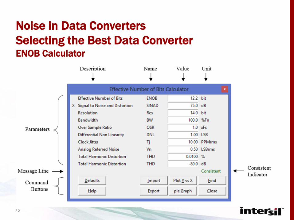
Noise in Data ConvertersSelecting the Best Data ConverterENOB Calculator
72

“Consistent” indicates all parameters are consistent, otherwise “Inconsistent” is displayed.
Noise in Data ConvertersSelecting the Best Data ConverterENOB Calculator Commands
73

The pie chart shows the contribution of each noise source in the data converter or signal chain.
Noise in Data ConvertersSelecting the Best Data ConverterENOB Calculator Pie Chart
74

The parametric plot allows trade-offs to be made between noise sources such that the total SINAD remains constant.
Noise in Data ConvertersSelecting the Best Data ConverterENOB Calculator Parametric Plot
75

Selecting the Best Data Converter for Your Noise BudgetStep 1: Objective
A noise budget is the allocation of noise within a signal chain that results in an acceptable SNR at the output.
Example – Customer Requirement
Select an ADC that exceeds a SINAD of 60dB and has a large signal (full scale) bandwidth of 0 to 500kHz
NDigital Output
ENOB, SINAD, DNL, THD
ADCAnalog Input, VN, BW
TJ
76

Selecting the Best Data Converter for Your Noise BudgetStep 2: Choose the Resolution• Start with the rule-of-thumb equation for an ideal data converter to find the
resolution required to achieve 60dB SNR.
• Using the ENOB calculator,
• Select 10 bits because real ADCs will have a lower SINAD since DNL, Tj, Vn, and THD are always greater than zero and will add noise.
dBNSNR 76.102.6 +=
60dB SNR → 9.7-bit 10-bit → 62dB SNR
02.676.1−
=SNRN→
77

Selecting the Best Data Converter for Your Noise BudgetStep 3: Selecting An Initial ADC
78
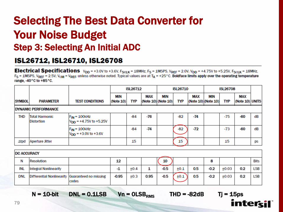
Selecting The Best Data Converter for Your Noise BudgetStep 3: Selecting An Initial ADC
Tj = 15psN = 10-bit DNL = 0.1LSB Vn = 0LSBRMS THD = -82dB79

Selecting The Best Data Converter for Your Noise BudgetStep 4: Calculating SINAD
The calculator defines Sample Jitter, Tj, as the ratio of the RMS jitter of the sample clock to the period of a full scale sine wave, in PPM.
where,
tJitter = 15ps
tIn = 1/500kHz = 2µs
610⋅=In
Jitter
ttTj
Therefore,
Expressing Tj in ppm
Input Sine Wave
Sample Clock tJitter = 15ps
tIn = 2µs
5.7101021015 6
6
12
=⋅⋅⋅
= −
−
Tj PPMrms
80

Selecting the Best Data Converter for Your Noise BudgetStep 4: Calculating SINAD
We find SINAD is 61.1dBIt meets our target with only a 1.1dB (14%) margin.
In practice, additional margin is needed because:
1. Typical values were used rather then Max (worst case)2. Have not allowed for the presence of additional noise sources
Enter the ISL26710’s parameters into the calculator:
1. N = 10-bit2. DNL = 0.1LSB3. Tj = 7.5PPM4. Vn = 0.00LSB5. THD = -84dB
81

Selecting the Best Data Converter for Your Noise BudgetStep 4: Calculating SINAD
We find SINAD is 58.3dB, below the 60dB budget.
Enter the ISL26710’s worst case parameters into the calculator:1. N = 10-bit2. DNL = 0.5LSB3. Tj = 7.5PPM4. Vn = 0.00LSB5. THD = -72dB
82

Selecting the Best Data Converter for Your Noise BudgetStep 5: Examining the Noise DistributionBy examining the relative noise and distortions levels, it is seen where improvements can be made.
• Additional improvements can be made by selecting the 12-bit version of the same device, the ISL26712, and thereby reduce the quantization noise.
• Quantization noise is the largest contributor to the total noise and distortion.
83

Selecting the Best Data Converter for Your Noise BudgetStep 6: Reducing the Quantization Noise
Tj = 15psN = 12-bit DNL = 0.95LSB Vn = 0LSBRMS THD = -74dB84

Selecting the Best Data Converter for Your Noise BudgetStep 6: Reducing the Quantization Noise
We find SINAD = 68.8dB It meets our target with a 8.8dB margin.
Enter the ISL26712’s worst case noise parameters into the calculator:1. N = 12-bit2. DNL = 0.5LSB3. Tj = 7.5PPM4. Vn = 0.0LSB5. THD = -74dB
85

Selecting the Best Data Converter for Your Noise BudgetStep 7: Re-examining the Noise DistributionRe-examining the worst case noise and distortions levels, we find the quantization noise comprises a smaller proportion of the noise source, but still dominates.
The total noise was reduced by 70% From 0.44LSBRMS at 10 bits To 0.53LSBRMS at 12 bits (equivalent to 0.13LSBRMS at 10-bit)
86

Selecting the Best Data Converter for Your Noise BudgetAn example of a higher resolution ADC
MAX1162 - ADC
Tj = 50psN = 16-bit DNL = 1.0LSB Vn = 0.65LSBRMS THD = -90dB
87

Selecting the Best Data Converter for Your Noise BudgetEntering Parameter Values
We find SINAD is 84.7dB
Enter the worst case MAX1162 parameters:1. N = 16-bit2. DNL = 1.0LSB3. Tj = 5PPM4. Vn = 0.65LSB5. THD = -90dB
88

Selecting the Best Data Converter for Your Noise BudgetExamining the Noise Distribution
Examining the worst case noise and distortion levels, we find an even distribution of noise, where no one source of noise stands out as a major contributor.
We see that at 14 to 16 bits, jitter and analog noise become as important as quantization noise and THD.
89

The calculator can plot any parameter with respect to another. Trade-offs can be made between noise sources that will result in the SINAD.
Selecting the Best Data Converter for Your Noise BudgetStep 8: Making Noise Distribution Trade-offs
• The cursor position indicates a trade-off between Vn and Tj that maintains a SINAD of 84.7dB.
• The cursor position indicates that if Tj can be decreased to 3.30PPM then the input noise can be increased to 0.85LSB and maintain the same SINAD of 84.7dB.
90

Understanding Noise in the Signal Chain Summary• The origin and characteristics of the noise sources
– Thermal noise– Shot noise– Avalanche noise– Flicker noise– Popcorn noise
• A tool for predicting noise amplitude over any bandwidth
• The origin and characteristics of data converter noise sources– Quantization noise– Aperture jitter – Harmonic distortion – Analog referred noise
• A tool for selecting the best data converter for a given noise
91

Understanding Noise in the Signal ChainDiscovery Questions• Is there a data converter in your signal chain? If so, what
is the resolution?
• What is the sample rate? – High frequency: Communications, wideband noise and distortion are
most important– Low frequency: Measurement and control, flicker noise and DC accuracy
are most important
• What are the noise requirements? Vrms, Vpp, SNR, SINAD, ENOB?
• What is the bandwidth of your channel?
92

The Thermal Noise and Effective Number of Bits (ENOB)calculators can be downloaded from Intersil’s website using the following URL: www.intersil.com/noise-calculators
Noise in Semiconductor Devices - Calculators
93

www.intersil.com