ultrahigh conductive copper/large flake size graphene
TRANSCRIPT

1704332 (1 of 8) © 2018 WILEY-VCH Verlag GmbH & Co. KGaA, Weinheim
CommuniCationwww.small-journal.com
Ultrahigh Conductive Copper/Large Flake Size Graphene Heterostructure Thin-Film with Remarkable Electromagnetic Interference Shielding Effectiveness
Zhe Wang, Boyang Mao, Qianlong Wang, Jun Yu, Jixiang Dai, Rongguo Song, Zonghua Pu, Daping He,* Zhi Wu, and Shichun Mu*
DOI: 10.1002/smll.201704332
and reliability.[3,4] Besides the thermal management challenge, the electromag-netic wave has a significant influence on the environment and human’s health.[5] Also, the electromagnetic wave disturbs electronic components and devices, and even renders them to lose functions.[6] Therefore, it is urgent to find out a mul-tifunctional interface material possessing excellent properties such as flexibility, ultrahigh electrical and thermal conduc-tivity, and superb electromagnetic inter-ference shielding effectiveness (EMI SE), which can be applied in next generation portable electronics and wearable devices.
Graphene, as a monolayer of carbon atoms bonded in a hexagonal lattice,[7,8] is the thinnest material with an extraor-dinary electrical and thermal conduc-tivity,[9] and has become one of the most studied materials these years.[10–13] In 2008, Balandin et al.[14] reported that the thermal conductivity (K) of a single layer graphene can be up to
4840–5300 W m−1 K−1 at room temperature (RT), and observ-ably outperformed other allotropes of carbon, such as single-wall carbon nanotube (SWCNT, K ≈3500 W m−1 K−1),[15] multi-wall carbon nanotube (MWCNT, K > 3000 W m−1 K−1),[16] and diamond (K = 800–2000 W m−1 K−1),[17] rendering graphene a remarkable candidate for thermal dispersing.[3] Hitherto, many graphene-based macroscopic materials (Table S1, Supporting Information), such as graphene films, graphene papers,
To guarantee the normal operation of next generation portable electronics and wearable devices, together with avoiding electromagnetic wave pollution, it is urgent to find a material possessing flexibility, ultrahigh conductive, and superb electromagnetic interference shielding effectiveness (EMI SE) simultaneously. In this work, inspired by a building bricks toy with the interlock system, we design and fabricate a copper/large flake size graphene (Cu/LG) composite thin film (≈8.8 μm) in the light of high temperature annealing of a large flake size graphene oxide film followed by magnetron sputtering of copper. The obtained Cu/LG thin-film shows ultrahigh thermal conductivity of over 1932.73 (±63.07) W m−1 K−1 and excellent electrical conductivity of 5.88 (±0.29) × 106 S m−1. Significantly, it also exhibits a remarkably high EMI SE of over 52 dB at the frequency of 1–18 GHz. The largest EMI SE value of 63.29 dB, accorded at 1 GHz, is enough to obstruct and absorb 99.99995% of incident radiation. To the best of knowledge, this is the highest EMI SE performance reported so far in such thin thickness of graphene-based materials. These outstanding properties make Cu/LG film a promising alternative building block for power electronics, microprocessors, and flexible electronics.
Graphene Based Films
Z. Wang, Dr. J. Yu, Z. H. Pu, Prof. D. P. He, Prof. S. C. MuState Key Laboratory of Advanced Technology for Materials Synthesis and ProcessingWuhan University of TechnologyWuhan 430070, ChinaE-mail: [email protected]; [email protected]. B. Y. MaoNational Graphene InstituteUniversity of ManchesterBooth Street East, Manchester M13 9PL, UK
The ORCID identification number(s) for the author(s) of this article can be found under https://doi.org/10.1002/smll.201704332.
Dr. Q. L. WangShenzhen Institute of Advanced Graphene Application and Technology (SIAGAT)Shenzhen 518106, ChinaDr. J. X. DaiNational Engineering Laboratory for Fiber Optic Sensing TechnologyWuhan University of TechnologyWuhan 430070, ChinaR. G. Song, Prof. D. P. He, Prof. Z. WuHubei Engineering Research Center of RF-Microwave Technology and ApplicationSchool of ScienceWuhan University of TechnologyWuhan 430070, China
Currently, commercial portable electronics, such as tablets, smartphones and light-emitting diode lamps, are more and more popular due to booming development of electronic and communication technologies.[1,2] However, with the trends toward miniaturization and high densities for the transistors and other integrated circuit devices, the improvement of com-puting power is at the expense of enhancing the thermal loss of devices and chips, which will result in a decline in performance
Small 2018, 14, 1704332

1704332 (2 of 8) © 2018 WILEY-VCH Verlag GmbH & Co. KGaA, Weinheim
www.advancedsciencenews.com www.small-journal.com
graphene fibers, and graphene-based nonwoven fabrics, have been investigated for thermal mana gement, and the K values were ranged from 826 to 1529 W m−1 K−1.[9,18–22] For example, Shen et al. vapored directly GO suspension to get GO film,[3] followed by keeping evaporation of water under appropriate heating (50–60 °C) and then under 2000 °C graphitization, the resulting graphite-like graphene film can achieve a high K at 1100 W m−1 K−1. Li and co-workers reported a hybrid structure by applying GO suspension scrapped on the surface of a copper foil,[4] after evaporated, carbonized at 3000 °C, and then pressed under mechanical pressing, the obtained graphene film had a K value of 1940 W m−1 K−1.
Regarding to EMI SE, graphene-based materials exhibit a high flexibility,[3,5,23] light weight,[5,24,25] and high electrical conductivity.[3,4] Graphene-based strucutres have attracted researchers’ attentions, especially in X-band (8–12 GHz) (Table S2, Supporting Information), which is extensively applied in medical demand, space research, satellites applied on communication service, earth exploration, and weather.[26,27] For instance, Al Ghamdi et al.[28] fabricated a polyvinyl chloride reinforced graphite/copper nanoparticles composite with a EMI SE of 50–70 dB at a thickness of 2 mm. Singh et al. further pre-pared graphene oxide/ferrofluid/cement composites,[29] whose EMI SE is 46 dB with a thickness of 2.5 mm. Recently, Hsiao et al. fabricated graphene nanosheet/water-borne polyurethane composites,[6] the EMI SE of this structure is 32 dB with a thick-ness of 2 mm. Table S2 in the Supporting Information sum-marizes other graphene-based electromagnetic shielding mate-rials, such as graphene/polymethyl methacrylate composites
(EMI SE of ≈30 dB and thickness of 3.4 mm),[30] (SWCNT/poly-aniline) and graphene sheet/polyaniline (EMI SE of 27–31 dB and thickness of 2.4 mm) and so on.[31] For the best of knowl-edge, the thickness of those fabricated materials is around 2–4 mm, which makes them impossibly be applied to portable devices.[3,25,32,33] However, it is still a big challenge to assemble nanoscale graphene sheets into a macroscopic material with high conductive and electromagnetic shielding properties.
Herein, we, for the first time report on a flexible Cu/large flake size graphene (Cu/LG) composite film. Such a film is syn-thesized by annealing a large flake size graphene oxide film at high temperatures and then coating it with a very thin layer of copper via magnetron sputtering. Inspired by a building bricks toy with the interlock system, we designed a similar structure to anchor Cu layer and graphene lamination. The introduced copper layer, as a kind of isotropic material, can promote the vertical heat transmission from heat source to anisotropic LG film quickly through copper. As expected, the formed Cu/LG composite film presents excellent flexibility, ultrahigh thermal and electrical conductivity, as well as remarkably high EMI SE.
As shown in Figure 1, the large flake size graphene oxide (LGO) film was separated from graphene oxide suspension after centrifugation. The prepared graphene film then went through high temperature annealing and rolling depression (Figure S1, Supporting Information). The formed LG film was then coated with a very thin layer of Cu via magnetron sputtering to obtain Cu/LG film.[34,35] The detailed synthesis routes that are widely and commonly used in both academic research and industry manufacture, can be found in the Experimental Section.
Small 2018, 14, 1704332
Figure 1. Fabrication process scheme of Cu/LG film.

1704332 (3 of 8) © 2018 WILEY-VCH Verlag GmbH & Co. KGaA, Weinheim
www.advancedsciencenews.com www.small-journal.com
It has been demonstrated that the size of graphene has an impact on the property of the graphene film.[36] For instance, the film consists of small flake size graphene and too many edges can restrict flexibility of the film. To demonstrate the flexibility, as shown in Figure 2a, LG film can be folded into a complex shape without breaking the structure. Figure 2b even presents that Cu/LG film is intensively bended, and the copper layer remains tightly coated on LG film without detachment after 100 times of bending tests. During the intense bending test with bending speed of 2 Hz and bending radius of ∞ (ini-tial) → 0 (bending) mm, the film is still with constant relative volume resistances and the electrical conductivity is unchanged (Figures S2 and S3, Supporting Information). The graphene side and Cu side of Cu/LG film are distinguished and labeled for further clarification. Figure 2c is the transmission electron microscope (TEM) image of a large flake size graphene with a diameter of ≈91 µm. Together with the optical microscopy image (Figure 2d) and corresponding size distributions (inset of Figure 2d), it can be observed that about 67% LG with a size of more than 75 µm, and 26.67% LG is more than 125 µm.
General strategies to obtain a Cu/graphene composite film, such as chemical vapor deposition on Cu foil or spark plasma sintering, always restrict the flexibility. In this work, inspired by a building bricks toy, one of the children’s favorite toy, that is a kind building blocks with the interlock system (Figure 2e) playing a significant role in toughening and strengthening, we designed a similar structure to link Cu layer and graphene lami-nation (Figure 2f). In such an inner-linked structure, it can be found that the surface of LG film is relatively rough with many
granular bubbles and microfolds (Figure 2g). In the annealing process, gases generated from undocked oxygen-containing functional groups, escape and form (sprouted) nanocavities and (matured) microcavities.[4] The formed nanocavities are thus fur-ther developed into granular bubbles (100–200 nm, Figure S4, Supporting Information), and the microcavities are evolved into microfolds from the compressing process due to the synergistic effect of graphene sheets stacking and defects-healing. Granular bubbles and microfolds on the surface of LG film are the equiv-alent of convex particles of building bricks, making LG tightly anchored on the coated copper layer in structure, increasing the contact area between LG and copper to enhance vertical heat conduction rate, and playing a positive role for EMI SE by pro-viding more interfaces for repeated reflection and scattering.[37] After copper decoration by magnetron sputtering, it can be seen that the surface of Cu/LG film becomes smooth (Figure 2h). The insets of Figure 2g,h are the scheme showing that heat con-ducts from heat resource through LG film slowly, while quickly for the Cu/LG film owing to the coated Cu layer. In the com-posite system, the coated Cu layer collects heat from the heat source as a sink, thus improving heat-dissipation speed. From the cross-section observation of scanning electron microscope (SEM) in Figure 2i, the thickness of LG film is 7.8 µm (standard controlled). About 1 µm thickness Cu layer was deposited onto graphene lamination by magnetron sputtering and obtained Cu/LG film (Figure 2j).
X-ray diffraction (XRD) analysis was carried out from the Cu side of Cu/LG film to obtain inner structure information about Cu/LG film. It can be observed that the diffraction peaks
Small 2018, 14, 1704332
Figure 2. Design of graphene film and its SEM images. a) Flexible LG film was folded into a frog; b) Cu/LG film in the status of bending; c) TEM image of a LG sheet; d) optical microscopy image and (inset in (d)) corresponding size distributions of LG sheets; e) optical image of building bricks; f) diagrammatic sketch and schematic diagram (the inset) of Cu/LG film surface; g) SEM image of the surface of LG film with many granular bubbles and microfolds and h) Cu/LG film, the insets are schematic diagram of heat conduction from heat resource through LG film and Cu/LG film, respectively; i) SEM image exhibiting a layer-by-layer structure in cross-sectional view of LG film; j) SEM image showing Cu coating and graphene lamination in cross-sectional view of Cu/LG film.
1704332 (4 of 8) © 2018 WILEY-VCH Verlag GmbH & Co. KGaA, Weinheim
www.advancedsciencenews.com www.small-journal.com
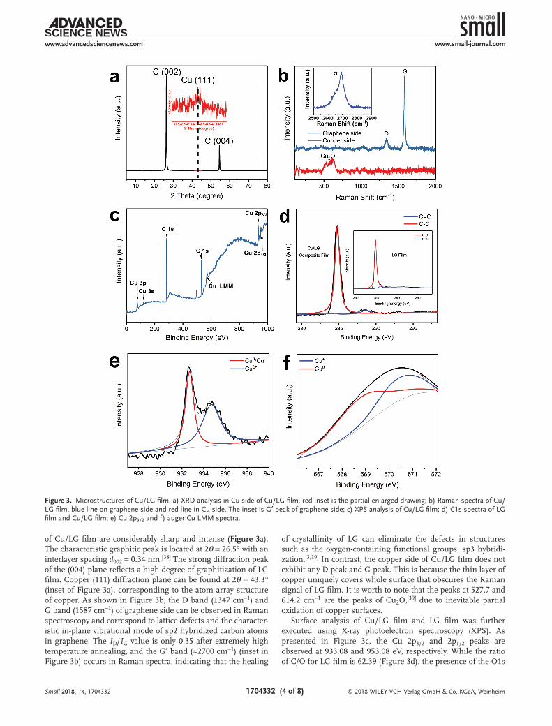
of Cu/LG film are considerably sharp and intense (Figure 3a). The characteristic graphitic peak is located at 2θ = 26.5° with an interlayer spacing d002 = 0.34 nm.[38] The strong diffraction peak of the (004) plane reflects a high degree of graphitization of LG film. Copper (111) diffraction plane can be found at 2θ = 43.3° (inset of Figure 3a), corresponding to the atom array structure of copper. As shown in Figure 3b, the D band (1347 cm−1) and G band (1587 cm−1) of graphene side can be observed in Raman spectroscopy and correspond to lattice defects and the character-istic in-plane vibrational mode of sp2 hybridized carbon atoms in graphene. The ID/IG value is only 0.35 after extremely high temperature annealing, and the G′ band (≈2700 cm−1) (inset in Figure 3b) occurs in Raman spectra, indicating that the healing
of crystallinity of LG can eliminate the defects in structures such as the oxygen-containing functional groups, sp3 hybridi-zation.[3,19] In contrast, the copper side of Cu/LG film does not exhibit any D peak and G peak. This is because the thin layer of copper uniquely covers whole surface that obscures the Raman signal of LG film. It is worth to note that the peaks at 527.7 and 614.2 cm−1 are the peaks of Cu2O,[39] due to inevitable partial oxidation of copper surfaces.
Surface analysis of Cu/LG film and LG film was further executed using X-ray photoelectron spectroscopy (XPS). As presented in Figure 3c, the Cu 2p3/2 and 2p1/2 peaks are observed at 933.08 and 953.08 eV, respectively. While the ratio of C/O for LG film is 62.39 (Figure 3d), the presence of the O1s
Small 2018, 14, 1704332
Figure 3. Microstructures of Cu/LG film. a) XRD analysis in Cu side of Cu/LG film, red inset is the partial enlarged drawing; b) Raman spectra of Cu/LG film, blue line on graphene side and red line in Cu side. The inset is G′ peak of graphene side; c) XPS analysis of Cu/LG film; d) C1s spectra of LG film and Cu/LG film; e) Cu 2p3/2 and f) auger Cu LMM spectra.

1704332 (5 of 8) © 2018 WILEY-VCH Verlag GmbH & Co. KGaA, Weinheim
www.advancedsciencenews.com www.small-journal.com
peak of Cu/LG film indicates oxidation of Cu in air after fab-rication. Figure 3e,f further presents that some Cu in Cu/LG film has been partly oxidized, which is in good agreement with the Raman spectrum results. Two peaks appear at 934.73 and 932.68 eV in the Cu 2p3/2 XPS spectra (Figure 3e). The higher binding energy (BE) peak at 934.73 eV suggests Cu2+ species in Cu/LG film, together with the characteristic Cu2+ shakeup satel-lite peaks (Figure S5, Supporting Information).[40,41] The lower BE peak at 932.68 eV is assigned to the presence of Cu+ or Cu0 species.[42,43] Cu 2p3/2 XPS spectra cannot differentiate between Cu+ and Cu0, hence, auger Cu LMM spectra (presented by the LMM electrons: the L layer electrons are aroused and become free electrons, then the M layer electrons fill the L layer, from which the energy released arouses another M layer electrons to form the auger electrons) (Figure 3f) were used to confirm the presence of Cu0 at BE 568.70 eV.[41]
As presented in Figure 4a, Cu/LG film possesses a superb electrical conductivity of 5.88 (±0.29) × 106 S m−1 (copper side) and 5.67 ± 0.32 × 10⁶ S m−1 (graphene side) amazingly increasing by ≈17.60% compared with that of LG film (5.00 ± 0.27 × 10⁶ S m−1), ascribed to the full filling of Cu in the inter-flake junction. The two values are mighty close ascribed to the extremely small thickness of the film. LG film and Cu/LG film are both much better than the previous reported: graphene films (1.06 × 10⁶ S m−1),[4] commercial graphite films (1.00 × 10⁶ S m−1),[3] graphene papers (1.00–2.23 × 10⁵ S m−1),[3,21,22,44,45] and other graphene-based films (Table S1, Supporting Information). In addition, the thermal conductivity of Cu/LG film is slightly larger than that of LG film (1932.73 ± 63.07 W m−1 K−1) (Figure 4b), close to the highest thermal con-ductivity (1940 W m−1 K−1) of graphene films,[4] much better than that of commercial graphite films (1750 W m−1 K−1),[3] and
Small 2018, 14, 1704332
Figure 4. Superb electrical and thermal conductivity of LG film and Cu/LG film used in smartphones. Comparison of a) electrical conductivity and b) the in-plane thermal conductivity of different graphene (graphite) film (or paper) with the result in this work. c) Infrared thermal photographs of Cu foil, Cu/LG film, LG film, and commercial graphite film; d) the optical image on the back of a smartphone; e) the smartphone utilizing Cu/LG film, f) LG film, g) nothing as the heat dissipation film.

1704332 (6 of 8) © 2018 WILEY-VCH Verlag GmbH & Co. KGaA, Weinheim
www.advancedsciencenews.com www.small-journal.com
other graphene papers or films (313–1529 W m−1 K−1)[3,21,22,44,46] (Table S1, Supporting Information). As copper possesses the different density and the specific heat capacity from LG film, the thermal conductivity of Cu/LG film is hardly to be meas-ured accurately by a traditional method. Nevertheless, infrared thermal photograph (Figure 4c) visually demonstrates that the heat-transfer rate of Cu/LG film is obviously faster than that of LG film, commercial graphite film, and Cu foil.
To further investigate the heat-transfer rate of Cu/LG film and LG film, they were used as the heat dissipation film in the smartphone (Figure 4d), respectively. Temperature was meas-ured with an infrared thermal imager. A certain application was worked for 30 min to generate heat. The smartphone without any thermal interface material (named as bare-smartphone, Figure 4g) was tested and show a temperature up to 47.7 °C,
while the smartphone with Cu/LG film (labeled as Cu/LG-smart-phone, Figure 4e) and the smartphone with LG film (entitled as LG-smartphone, Figure 4f) exhibit the peak-temperatures of mere 40.8 and 43.6 °C, which is 6.9 and 4.1 °C lower than that of bare-smartphone, respectively. It can be observed that the temperature of Cu/LG-smartphone distributes much more uniformly than that of bare-smartphone, and slightly better than that of LG-smart-phone. Therefore, Cu/LG film has a better thermal transfer rate, thus homogenizing and reducing the heat produced by the chips.
Besides electrical and thermal conductivity, the EMI SE per-formance of Cu/LG film was fully investigated from L-band to Ku-band via the coaxial line with a Network Analyzer (PNA-X, N5247A). The measuring instrument and the schematic dia-gram of coaxial line are shown in Figure 5a,b, respectively. As presented in Figure 5c–e, Cu/LG film exhibits excellent
Small 2018, 14, 1704332
Figure 5. Remarkable EMI SE of Cu/LG film. a) The optical image of Network Analyzer; b) the diagrammatic sketch of coaxial line and three scenarios about EMI shielding mechanism of Cu/LG film; c–e) the EMI SE of Cu foil, LG film, and Cu/LG film at L-band (1–2 GHz), S-band (2–4 GHz), C-band (4–8 GHz) for (c), X-band (8–12 GHz) for (d), Ku-band (12–18 GHz) for (e), respectively; f) EMI SE−Absorption (%) of Cu/LG film and Cu foil.

1704332 (7 of 8) © 2018 WILEY-VCH Verlag GmbH & Co. KGaA, Weinheim
www.advancedsciencenews.com www.small-journal.com
EMI SE from 1 to 18 GHz, including L-band (1–2 GHz), S-band (2–4 GHz), C-band (4–8 GHz), X-band (8–12 GHz), Ku-band (12–18 GHz) according to IEEE 521–2002 standard. Thereinto, the L-band is suitable for digital audio broadcasting, mobile communication, and satellite navigation systems. In L-band (Figure 5c), in terms of the EMI SE, Cu/LG film shows a 61.39–63.29 dB which has an obvious advantage over LG film. The highest EMI SE value of 63.29 dB was recorded at 1 GHz, enough to block and absorb 99.99995% of incident electromag-netic wave with only 0.00005% transmission. In addition, the S-band is applied to relay, satellite communication and radar and the C band is utilized for satellite television broadcasting and small satellite ground stations. In both S-band and C-band, the EMI SE value of Cu/LG film is larger than that of LG film and Cu foil. The space applications of X-band include space research, broadcast satellite, fixed communication service satel-lite, earth exploration satellite, and weather satellite. In X-band (Figure 5d), the EMI SE values of Cu/LG film, LG film, and Cu foil are slightly larger than 52, 37, 30 dB, respectively. Ku-band can be applied to satellite digital broadcasting. As to the EMI SE in Ku-band, Cu/LG film could block and absorb 99.99934%–99.99959% of incident electromagnetic wave (Figure 5e), which is larger than LG film, and they are both much better than Cu foil. Therefore, regardless of the band range, Cu/LG film is the best in all performance. Consequently, Cu/LG film maintains prominent EMI SE (more than 52 dB) over an ultrawide fre-quency range (1–18 GHz), and the largest EMI SE value of 63.29 dB recorded at 1 GHz. In addition, the EMI SE of Cu/LG film can still maintain more than 49.02 dB after 100 times bending (Figure S6, Supporting Information), enough to block and absorb 99.99875% of incident radiation with only 0.00125% transmission. Therefore, Cu/LG film exhibits promising EMI SE stability.
The EMI SE of Cu side and graphene side of Cu/LG film is almost same (Figure S7, Supporting Information). Nevertheless, the graphene side is chosen deliberately toward extraneous elec-tromagnetic wave to decrease electromagnetic wave pollution. When electromagnetic wave reaches the surface of Cu/LG film, it could result in three scenarios (Figure 5b): (1) absorbed and attenuated repeatedly in the interior of LG film; (2) reflected into LG film from surface of Cu layer and then absorbed and attenu-ated repeatedly in LG film; (3) reflected again and again and attenuated in Cu coating layer. According to Figure 5f, EMI SE-absorption of Cu foil is less than 10%, indicating that shielding mechanism of Cu is rather reflection than absorption. In addi-tion, the absorption of electromagnetic wave of Cu/LG film at 1–18 GHz is more than 90%, suggesting that the main EMI shielding mechanisms of Cu/LG film is in scenario (1) and (2), namely absorption of electromagnetic wave. This avoids electro-magnetic wave to be reflected to the surrounding environment that increases electromagnetic wave pollution. More detailed mechanisms base on complex permittivity (real part ε′ and imagi-nary part ε′′) and loss tangent (tan δ) are discussed in Figures S8 and S9 in the Supporting Information.[47]
The LG film consists of large flake size graphene, which avoids the low quality or/and high interflake junction contact resistance that normally happens in small flake size graphene-based structures. Together with Cu full filling in the interflake junction, the electrical conductivity increases remarkably.[48]
The boundary scattering of phonon and phonon-defect are greatly reduced in LG film, thus leading to improving dramati-cally the thermal conductivity. In addition, pure copper, as a kind of isotropic material, is one of the best metallic thermal conductors (K = 401 W m−1 K−1 at RT), whatever in horizontal or in vertical. Vertical (perpendicular to the plane) heat trans-mission from heat source to LG film can be achieved quickly through copper, and then the problem of vertical heat conduc-tion is solved in an overturn way. Significantly, the heat capacity of Cu is ≈2.18 times than that of LG film (seen at analysis of thermal conductivity enhancement in the Supporting Informa-tion). Cu transfers heat quickly from the heat source to itself and accumulate as a heat sink, thus allowing chips or other heat sources to reduce temperature rapidly. In the meantime, LG film dissipates heat by exchanging heat with air in terms of its excellent thermal conductivity. This can be indirectly proved through that Cu side of Cu/LG film surpasses graphene side in terms of heat dissipation performance (Figure S10, Supporting Information). Analogously, LG enhances the absorption of electromagnetic wave and Cu reflects residual electromagnetic wave as the second protective parclose.
In summary, we provide a novel synthetic method to deal with the problem of integrating high electrical and thermal conductivity, flexibility, and excellent EMI SE together into one macroscopic material. Significantly, a physical vapor deposi-tion method of magnetron sputtering is introduced to control the thickness of coating Cu layer, and make LG film and Cu layer integrated strongly with each other. Thereinto, nano-bubbles and microfolds on graphene lamination surface are utilized to anchor themselves with Cu coating layer tightly. The resulted film exhibits ultrahigh thermal conductivity (over 1932.73 ± 63.07 W m−1 K−1) and electrical conductivity (5.88 ± 0.29 × 10⁶ S m−1), as well as superb EMI SE (over 52 dB at 1–18 GHz, especially 63.29 dB at 1 GHz, enough to block and absorb 99.99995% of incident radiation with only 0.00005% transmission) with a thickness of 9 ± 1.5 µm. With such eminent properties, Cu/LG film becomes a kind of promising candidate for flexible electronics, power electronics, and micro-processors. We believe this new film can raise the wide inter-ests of all related working in academic and industrial societies.
Experimental SectionPreparation of LG Film: The LGO was prepared from the suspension
of GO (purchased from Wuxi chengyi education technology Co. Ltd.) using a centrifugal classification method, which was described in the ref. [4]. The suspension of GO was diluted with ultrapure water to 2 mg mL−1. The bottom solution (30% in volume) was reserved after centrifugation at 5000 rpm for 30 min, then diluted to 2 mg mL−1 again for the next cycle of centrifugal classification. Repeating aforementioned operations for seven times, the last bottom gel was retained, and subsequently diluted with ultrapure water to 10–20 mg mL−1 and scraped on the surface of polyethylene terephthalate (PET) film, evaporated for 24 h at room temperature, and the GO film was fabricated. The GO film was high temperature annealed at temperature of 1300 °C for 2 h, 3000 °C for 1 h, both under protection of Ar gas flow, followed by rolling compressed to synthesize a packed LGO film with shiny lustre. The density of LG film is 2.1 g cm−3.
Preparation of Cu/Large Flake Size Graphene Film: To fabricate Cu/LG film, Cu thin films were sputtered on the surface of LG film by using a BESTECH sputtering system. During the depositing process, the
Small 2018, 14, 1704332

1704332 (8 of 8) © 2018 WILEY-VCH Verlag GmbH & Co. KGaA, Weinheim
www.advancedsciencenews.com www.small-journal.com
thickness of hydrogen sensitive film was monitored by quartz crystal method. Under 0.5 Pa sputtering pressure of Ar, the deposition power for Cu targets is 100 W, and the corresponding deposition rate is 0.039 nm s−1.
Supporting InformationSupporting Information is available from the Wiley Online Library or from the author.
AcknowledgementsZ.W., B.Y.M., and Q.L.W. contributed equally to this work. This work was supported by the National Natural Science Foundation of China (Grant no. 51372186, 51672204, 51701146, 51402228). The authors also acknowledge the Center for Materials Research and Analysis of Wuhan University of Technology for TEM (Dr. Zhao Deng) and picture suggestions.
Conflict of InterestThe authors declare no conflict of interest.
Keywordselectrical conductivity, electromagnetic interference shielding, films, large flake size graphene, thermal conductivity
Received: December 13, 2017Revised: February 1, 2018
Published online: April 17, 2018
[1] Z. Yan, G. Liu, J. M. Khan, A. A. Balandin, Nat. Commun. 2012, 3, 827.[2] A. A. Balandin, Nat. Mater. 2011, 10, 569.[3] B. Shen, W. Zhai, W. Zheng, Adv. Funct. Mater. 2014, 24, 4542.[4] L. Peng, Z. Xu, Z. Liu, Y. Guo, P. Li, C. Gao, Adv. Mater. 2017, 29, 27.[5] Z. Chen, C. Xu, C. Ma, W. Ren, H. M. Cheng, Adv. Mater. 2013, 25,
1296.[6] S. T. Hsiao, C. C. M. Ma, H. W. Tien, W. H. Liao, Y. S. Wang,
S. M. Li, Y. C. Huang, Carbon 2013, 60, 57.[7] A. K. Geim, K. S. Novoselov, Nat. Mater. 2007, 6, 183.[8] Y. Wang, N. Xu, D. Li, J. Zhu, Adv. Funct. Mater. 2017, 27, 19.[9] G. Xin, T. Yao, H. Sun, S. M. Scott, D. Shao, G. Wang, J. Lian,
Science 2015, 349, 1083.[10] D. He, H. Tang, Z. Kou, M. Pan, X. Sun, J. Zhang, S. Mu, Adv.
Mater. 2017, 29, 20.[11] Z. Kou, T. Meng, B. Guo, I. S. Amiinu, W. Li, J. Zhang, S. Mu, Adv.
Funct. Mater. 2017, 27, 1604904.[12] H. Zhou, J. Zhang, I. S. Amiinu, C. Zhang, X. Liu, W. Tu, M. Pan,
S. Mu, Phys. Chem. Chem. Phys. 2016, 18, 10392.[13] X. Liu, I. S. Amiinu, S. Liu, K. Cheng, S. Mu, Nanoscale Res. Lett.
2013, 8, 27.[14] A. A. Balandin, S. Ghosh, W. Bao, I. Calizo, D. Teweldebrhan,
F. Miao, C. N. Lau, Nano Lett. 2008, 8, 902.[15] E. Pop, D. Mann, Q. Wang, K. Goodson, H. Dai, Nano Lett. 2006,
6, 96.
[16] P. Kim, L. Shi, A. Majumdar, P. L. McEuen, Phys. Rev. Lett. 2001, 87, 215502.
[17] A. V. Sukhadolau, E. V. Ivakin, V. G. Ralchenko, A. V. Khomich, A. V. Vlasov, A. F. Popovich, Diamond Relat. Mater. 2005, 14, 589.
[18] Y. Huang, Q. Gong, Q. Zhang, Y. Shao, J. Wang, Y. Jiang, M. Zhao, D. Zhuang, J. Liang, Z. Ni, V. A. Danner, T. Li, L. Hu, Nanoscale 2017, 9, 2340.
[19] J. Zhang, G. Shi, C. Jiang, S. Ju, D. Jiang, Small 2015, 11, 6197.[20] Q. Q. Kong, Z. Liu, J. G. Gao, C. M. Chen, Q. Zhang, G. Zhou,
Z. C. Tao, X. H. Zhang, M. Z. Wang, F. Li, R. Cai, Adv. Funct. Mater. 2014, 24, 4222.
[21] G. Xin, H. Sun, T. Hu, H. R. Fard, X. Sun, N. Koratkar, T. Borca Tasciuc, J. Lian, Adv. Mater. 2014, 26, 4521.
[22] C. Teng, D. Xie, J. Wang, Z. Yang, G. Ren, Y. Zhu, Adv. Funct. Mater. 2017, 27, 1700240.
[23] W. L. Song, M. S. Cao, M. M. Lu, S. Bi, C. Y. Wang, J. Liu, J. Yuan, L. Z. Fan, Carbon 2014, 66, 67.
[24] B. Wen, M. Cao, M. Lu, W. Cao, H. Shi, J. Liu, X. Wang, H. Jin, X. Fang, W. Wang, J. Yuan, Adv. Mater. 2014, 26, 3484.
[25] J. Ling, W. Zhai, W. Feng, B. Shen, J. Zhang, W. G. Zheng, ACS Appl. Mater. Interfaces 2013, 5, 2677.
[26] X. Liu, Z. Zhang, Y. Wu, Composites, Part B 2011, 42, 326.[27] N. Joseph, M. T. Sebastian, Mater. Lett. 2013, 90, 64.[28] A. A. Al-Ghamdi, F. El-Tantawy, Composites, Part A 2010, 41, 1693.[29] A. P. Singh, M. Mishra, A. Chandra, S. K. Dhawan, Nanotechnology
2011, 22, 465701.[30] H. Bin Zhang, W. G. Zheng, Q. Yan, Z. G. Jiang, Z. Z. Yu, Carbon
2012, 50, 5117.[31] B. Yuan, L. Yu, L. Sheng, K. An, X. Zhao, J. Phys. D: Appl. Phys. 2012,
45, 235108.[32] J. Liang, Y. Wang, Y. Huang, Y. Ma, Z. Liu, J. Cai, C. Zhang, H. Gao,
Y. Chen, Carbon 2009, 47, 922.[33] H. Zhang, Q. Yan, W. Zheng, Z. He, Z. Yu, ACS Appl. Mater. Inter-
faces 2011, 3, 918.[34] J. Dai, M. Yang, Z. Yang, Z. Li, Y. Wang, G. Wang, Y. Zhang,
Z. Zhuang, Sens. Actuators, B 2014, 196, 604.[35] H. Song, Y. Chen, G. Zhang, Y. Liu, P. Huang, H. Zhao, M. Yang,
J. Dai, Z. Li, Sens. Actuators, B 2015, 216, 11.[36] Q. Yang, Y. Su, C. Chi, C. T. Cherian, K. Huang, V. G. Kravets,
F. C. Wang, J. C. Zhang, A. Pratt, A. N. Grigorenko, F. Guinea, A. K. Geim, R. R. Nair, Nat. Mater. 2017, 16, 1198.
[37] J. Liu, H. B. Zhang, R. H. Sun, Y. F. Liu, Z. S. Liu, A. G. Zhou, Z. Z. Yu, Adv. Mater. 2017, 29, 1702367.
[38] H. C. Semmelhack, R. Höhne, P. Esquinazi, G. Wagner, A. Rahm, K. H. Hallmeier, D. Spemann, K. Schindler, Carbon 2006, 44, 3064.
[39] Y. S. Gong, C. Lee, C. K. Yang, T. Cu, J. Appl. Phys. 1995, 2, 10.[40] P. Liu, E. J. M. Hensen, J. Am. Chem. Soc. 2013, 135, 14032.[41] I. Platzman, R. Brener, H. Haick, R. Tannenbaum, J. Phys. Chem. C
2008, 112, 1101.[42] M. C. Biesinger, L. W. M. Lau, A. R. Gerson, R. S. C. Smart, Appl.
Surf. Sci. 2010, 257, 887.[43] K. L. Deutsch, B. H. Shanks, J. Catal. 2012, 285, 235.[44] H. Wu, L. T. Drzal, Carbon 2012, 50, 1135.[45] R. G. Song, Q. L. Wang, B. Y. Mao, Z. Wang, D. L. Tang, B. Zhang,
J. W. Zhang, C. G. Liu, D. P. He, Z. Wu, S. C. Mu, Carbon 2018, 130, 164.
[46] N. J. Song, C. M. Chen, C. Lu, Z. Liu, Q. Q. Kong, R. Cai, J. Mater. Chem. A 2014, 2, 16563.
[47] B. Wen, M. S. Cao, Z. L. Hou, W. L. Song, L. Zhang, M. M. Lu, H. B. Jin, X. Y. Fang, W. Z. Wang, J. Yuan, Carbon 2013, 65, 124.
[48] Z. Chen, W. Ren, L. Gao, B. Liu, S. Pei, H. M. Cheng, Nat. Mater. 2011, 10, 424.
Small 2018, 14, 1704332