twr-s08 - rab.ict.pwr.wroc.plrab.ict.pwr.wroc.pl/~mw/lster/twr-s08ll_lh_ug.pdft w r - s 0 8 l l / l...
TRANSCRIPT

D O C - 0 5 0 0 - 0 1 0 , R E V C
Web Site: www.axman.com
Support: [email protected]
TWR-S08
Demonstration Board for Freescale MC9S08LL and MC9S08LH Families of Microcontrollers
USER GUIDE
T W R - S 0 8 L L / L H U S E R G U I D E O C T O B E R 6 , 2 0 0 9
U S E R G U I D E
2
CONTENTS
CAUTIONARY NOTES .............................................................................................................. 4
TERMINOLOGY ......................................................................................................................... 4
FEATURES ................................................................................................................................ 5
REFERENCES ........................................................................................................................... 6
GETTING STARTED .................................................................................................................. 6
MEMORY MAP .......................................................................................................................... 6
SOFTWARE DEVELOPMENT ................................................................................................... 6
DEVELOPMENT SUPPORT ...................................................................................................... 6
OSBDM BOOTLOADER ........................................................................................................ 7
BDM_PORT HEADER ........................................................................................................... 7
POWER ...................................................................................................................................... 7
POWER SELECT .................................................................................................................. 8 V_SEL ............................................................................................................................... 8
VDD_EN ............................................................................................................................ 8
RESET SWITCH ........................................................................................................................ 9
LOW VOLTAGE RESET ............................................................................................................ 9
TIMING ....................................................................................................................................... 9
COMMUNICATIONS .................................................................................................................. 9
RS-232 ................................................................................................................................ 10
COM CONNECTOR ........................................................................................................ 10 COM_SEL ....................................................................................................................... 10
LCD .......................................................................................................................................... 11
ACCELEROMETER ................................................................................................................. 11
CONFIGURATION............................................................................................................... 11
USER I/O .................................................................................................................................. 12
VDD1 ENABLE ................................................................................................................ 12 BUZZER .......................................................................................................................... 12
LIGHT SENSOR .............................................................................................................. 12 PUSHBUTTON SWITCHES ............................................................................................ 13
USER LED’S ................................................................................................................... 13 POTENTIOMETER .......................................................................................................... 14
EDGE CONNECTOR PIN-OUT ................................................................................................ 14
T W R - S 0 8 L L / L H U S E R G U I D E O C T O B E R 6 , 2 0 0 9
U S E R G U I D E
3
FIGURES Figure 1: BDM_PORT Header, J400 .......................................................................................... 7
Figure 2: V_SEL Option Header, JP8 ......................................................................................... 8 Figure 3: VDD_EN Option Header, JP9...................................................................................... 9
Figure 4: COM Signal Connections .......................................................................................... 10 Figure 5: COM_PORT Connector, J3 ....................................................................................... 10
Figure 6: COM_SEL Option Header, JP5 ................................................................................. 10 Figure 7: Accelerometer Sensitivity Select , JP6 ...................................................................... 11
Figure 8: Accelerometer Output Cut-Traces ............................................................................. 11 Figure 9: USER1 Option Header, JP7 ...................................................................................... 12
Figure 10: Pushbutton Switch Signal Connections ................................................................... 13 Figure 11: USER2 Option Header, JP11 .................................................................................. 13
Figure 12: POT Enable Option Header, JP12 ........................................................................... 14 Figure 13: Primary Edge Connector, J1................................................................................... 14
Figure 14: Secondary Edge Connector, J2 ............................................................................... 16
REVISION Date Rev Comments
October 5, 2009 A Initial Release
October 6, 2009 B Updated board name to TWR-S08 thru-out
October 7, 2009 C Updated References section to correct document names and remove Support CD. Updated Figures to show board reference designators

T W R - S 0 8 L L / L H U S E R G U I D E O C T O B E R 6 , 2 0 0 9
U S E R G U I D E
4
CAUTIONARY NOTES
1) Electrostatic Discharge (ESD) prevention measures should be used when handling this product. ESD damage is not a warranty repair item.
2) Axiom Manufacturing does not assume any liability arising out of the application or use of any product or circuit described herein; neither does it convey any license under patent rights or the rights of others.
3) EMC Information on the TWR-S08 board:
a) This product as shipped from the factory with associated power supplies and cables, has been verified to meet with requirements of CE and the FCC as a CLASS A product.
b) This product is designed and intended for use as a development platform for hardware or software in an educational or professional laboratory.
c) In a domestic environment, this product may cause radio interference in which case the user may be required to take adequate prevention measures.
d) Attaching additional wiring to this product or modifying the products operation from the factory default as shipped may effect its performance and cause interference with nearby electronic equipment. If such interference is detected, suitable mitigating measures should be taken.
TERMINOLOGY
This development module utilizes option select jumpers to configure default board operation. Terminology for application of the option jumpers is as follows:
Jumper – a plastic shunt that connects 2 terminals electrically
Jumper on, in, or installed = jumper is a plastic shunt that fits across 2 pins and the shunt is installed so that the 2 pins are connected with the shunt.
Jumper off, out, or idle = jumper or shunt is installed so that only 1 pin holds the shunt, no 2 pins are connected, or jumper is removed. It is recommended that the jumpers be placed idle by installing on 1 pin so they will not be lost.
Cut-Trace – a circuit trace connection between component pads. The circuit trace may be cut using a knife to break the default connection. To reconnect the circuit, simply install a suitably sized 0-ohm resistor or attach a wire across the pads.
Signal names followed by an asterisk (*) denote active-low signals.
T W R - S 0 8 L L / L H U S E R G U I D E O C T O B E R 6 , 2 0 0 9
U S E R G U I D E
5
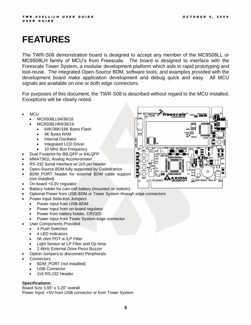
FEATURES
The TWR-S08 demonstration board is designed to accept any member of the MC9S08LL or MC9S08LH family of MCU’s from Freescale. The board is designed to interface with the Freescale Tower System, a modular development platform which aids in rapid prototyping and tool-reuse. The integrated Open-Source BDM, software tools, and examples provided with the development board make application development and debug quick and easy. All MCU signals are available on one or both edge connectors.
For purposes of this document, the TWR-S08 is described without regard to the MCU installed. Exceptions will be clearly noted.
MCU
MC9S08LL64/36/16
MC9S08LH64/36/16
64K/36K/16K Bytes Flash
4K Bytes RAM
Internal Oscillator
Integrated LCD Driver
10 MHz Bus Frequency
Dual Footprint for 80LQFP or 64LQFP
MMA7361L Analog Accelerometer
RS-232 Serial Interface w/ 2x5 pin header
Open-Source BDM fully supported by CodeWarrior
BDM_PORT header for external BDM cable support (not installed)
On-board +3.3V regulator
Battery holder for coin-cell battery (mounted on bottom)
Optional Power from USB-BDM or Tower System through edge connectors
Power Input Selection Jumpers
Power input from USB-BDM
Power input from on-board regulator
Power from battery holder, CR2325
Power input from Tower System edge connector
User Components Provided
4 Push Switches
4 LED Indicators
5K ohm POT w /LP Filter
Light Sensor w/ LP Filter and Op Amp
2.4kHz External Drive Piezo Buzzer
Option Jumpers to disconnect Peripherals
Connectors
BDM_PORT (not installed)
USB Connector
2x5 RS-232 Header Specifications: Board Size 3.55” x 3.20” overall Power Input: +5V from USB connector or from Tower System

T W R - S 0 8 L L / L H U S E R G U I D E O C T O B E R 6 , 2 0 0 9
U S E R G U I D E
6
REFERENCES Reference documents are provided on the LL64 DVD in Acrobat Reader format. This documentation may also be downloaded fromwww.axman.com/support. TWR-S08LL_LH_UG.pdf TWR-S08 User Guide (this document) TWR_9S08LL64_QSG.pdf TWR-S08 Quick Start Guide TWR9S08LL_SCH_B.pdf TWR-S08_LL_LH Schematic Rev. B TWR_MC9S08LL_LH_Silk.pdf TWR-S08_LL_LH Top Silk, Rev B TWRLL64_Quick_Start.zip CW LCD Demo Program Source Code TWR_9S08LL64_Lab.pdf Lab Tutorial for use with Quick Start Example Code
GETTING STARTED
To get started quickly, please refer to the TWR-S08_QSG Quick Start Guide. This quick start will illustrate connecting the board to a PC, installing the correct version of CodeWarrior Development Studio, and running a simple LCD program.
MEMORY MAP
The TWR-S08 is designed to support the complete line of MC9S08LL and MC9S08LH MCU’s. Refer to the associated target MCU Reference Manual (RM) for details on the target MCU memory map.
SOFTWARE DEVELOPMENT
Software development requires the use of a compiler or an assembler supporting the HCS08 instruction set and a host PC operating a debug interface. CodeWarrior Development Studio for Microcontrollers is supplied with this board for application development and debug.
DEVELOPMENT SUPPORT
Application development and debug for the target TWR-S08 board is supported through the Open-Source Background Debug Mode (OSBDM) interface. The OSBDM is fully supported in CodeWarrior and provides direct, non-intrusive access to the target device internals. While in BDM mode, no internal resources are used. Code stepping and break-points are fully supported.
Connection between a host PC and the target device is provided via a mini-B, USB connector. The OSBDM is capable of providing power to the target board eliminating the need for external
T W R - S 0 8 L L / L H U S E R G U I D E O C T O B E R 6 , 2 0 0 9
U S E R G U I D E
7
power. Please note that power supplied by the OSBDM is limited by the USB specification. When powered through the OSBDM, total current draw, including the OSBDM, TWR-S08 board, and Tower System must remain less that 500mA. Otherwise, the USB bus will cause the host PC to disconnect the board. Damage to the host PC, target board, or Tower System may result if this current limit is violated.
CAUTION:
When powered from the USB bus, do not exceed the 500mA maximum allowable current drain. Damage to the target board or host PC may result
OSBDM Bootloader
The OSBDM is pre-programmed with a bootloader application to allow field updates. The USB bootloader communicates with a GUI application running on a host PC. The GUI application enables OSBDM firmware to be updated at any. Option jumper JP400 enables the bootloader at startup. Option header JP400 is not populated in default configuration. Refer to Freescale Application Note AN3561 for details on using the GUI application and bootloader. The application note may be found at www.freescale.com or at www.axman.com/support.
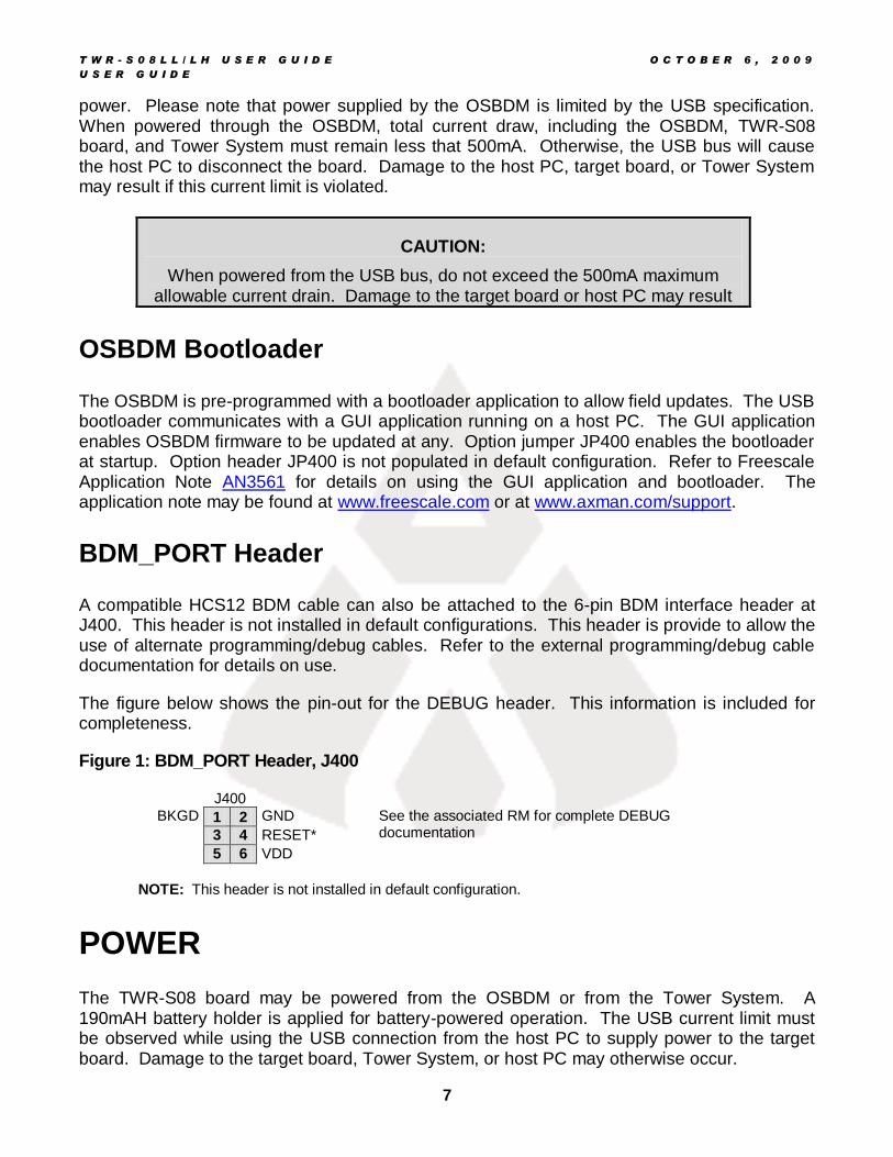
BDM_PORT Header
A compatible HCS12 BDM cable can also be attached to the 6-pin BDM interface header at J400. This header is not installed in default configurations. This header is provide to allow the use of alternate programming/debug cables. Refer to the external programming/debug cable documentation for details on use.
The figure below shows the pin-out for the DEBUG header. This information is included for completeness.
Figure 1: BDM_PORT Header, J400
J400
BKGD 1 2 GND See the associated RM for complete DEBUG documentation 3 4 RESET*
5 6 VDD
NOTE: This header is not installed in default configuration.
POWER
The TWR-S08 board may be powered from the OSBDM or from the Tower System. A 190mAH battery holder is applied for battery-powered operation. The USB current limit must be observed while using the USB connection from the host PC to supply power to the target board. Damage to the target board, Tower System, or host PC may otherwise occur.

T W R - S 0 8 L L / L H U S E R G U I D E O C T O B E R 6 , 2 0 0 9
U S E R G U I D E
8
POWER SELECT
Option headers V_SEL and VDD_EN select the source of input power to the target board. When powered from the Tower System, the OSBDM voltage output is disabled.
V_SEL
The V_SEL option header allows the user to select power input either the on-board regulator or the battery holder. The on-board regulator is supplied from the OSBDM voltage output. Figure 2 below shows the PWR_SEL header settings.
Figure 2: V_SEL Option Header, JP8
VR1 Enables voltage input from on-board regulator. This option should be selected when powered from the integrated OSBDM (default)
BATT
JP
8
VR1 Enables voltage input from battery holder. This option should be selected when battery-powered operation is desired
BATT
JP
8
Power from the integrated BDM is drawn from the USB bus and is limited to 500 mA total. This current limit accounts for the total current supplied over the USB cable to the BDM circuit, the target board, and any connected circuitry. Current drain in excess of 500 mA violates the USB specification and causes the USB bus to disconnect the offending device. This may cause the board to exhibit power cycling where the board appears to turn on then off continually. In this case, LED400 will flash on and off. If this condition is allowed to persist, damage to the host PC or the target board result.
The on-board voltage regulator (VR1) creates the +3.3V rails used by the target MCU from the +5V input provided by the OSBDM.
The battery holder at BATT accepts a 3.3V, 23mm, 190mAH lithium, coin-cell battery, PN CR-2325.
VDD_EN
The VDD_EN option header enables and disables VDD to the target board peripherals. Power to the MCU is unaffected by this option jumper. Removing this option jumper, along with others, allows the user to take accurate MCU current measurements. The figure below shows the VDD_EN option jumper connections.
T W R - S 0 8 L L / L H U S E R G U I D E O C T O B E R 6 , 2 0 0 9
U S E R G U I D E
9
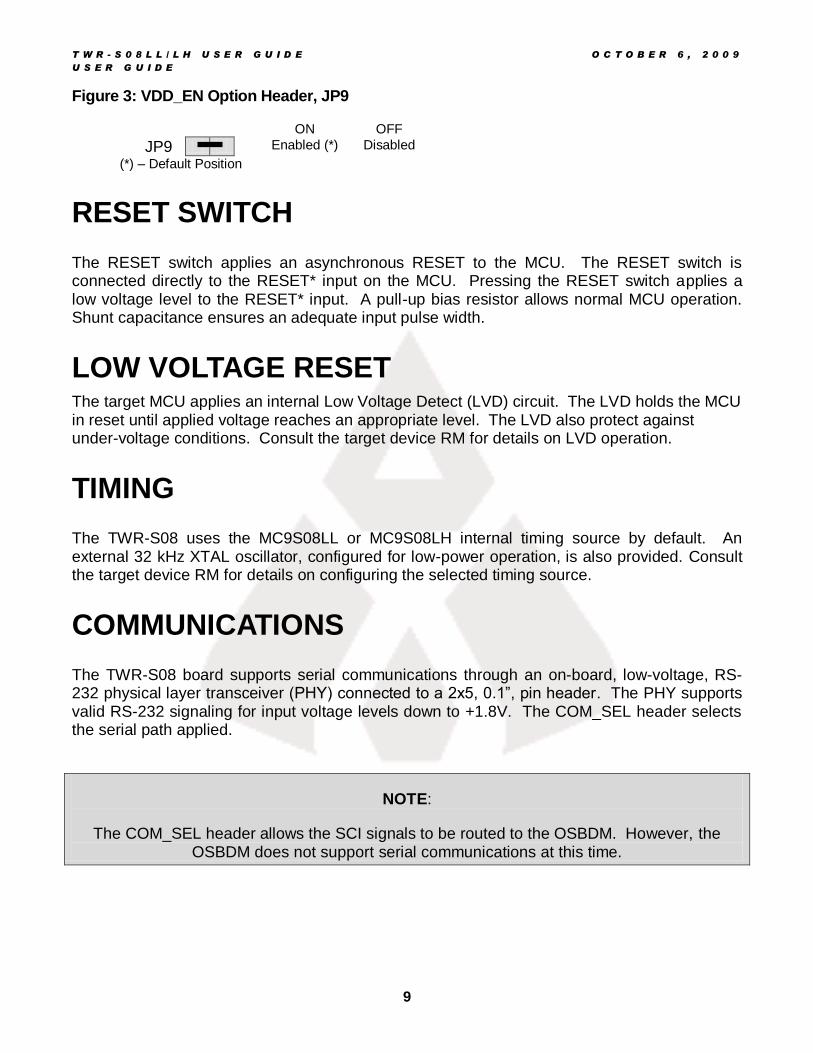
Figure 3: VDD_EN Option Header, JP9
ON OFF
JP9 Enabled (*) Disabled
(*) – Default Position
RESET SWITCH
The RESET switch applies an asynchronous RESET to the MCU. The RESET switch is connected directly to the RESET* input on the MCU. Pressing the RESET switch applies a low voltage level to the RESET* input. A pull-up bias resistor allows normal MCU operation. Shunt capacitance ensures an adequate input pulse width.
LOW VOLTAGE RESET The target MCU applies an internal Low Voltage Detect (LVD) circuit. The LVD holds the MCU in reset until applied voltage reaches an appropriate level. The LVD also protect against under-voltage conditions. Consult the target device RM for details on LVD operation.
TIMING
The TWR-S08 uses the MC9S08LL or MC9S08LH internal timing source by default. An external 32 kHz XTAL oscillator, configured for low-power operation, is also provided. Consult the target device RM for details on configuring the selected timing source.
COMMUNICATIONS
The TWR-S08 board supports serial communications through an on-board, low-voltage, RS-232 physical layer transceiver (PHY) connected to a 2x5, 0.1”, pin header. The PHY supports valid RS-232 signaling for input voltage levels down to +1.8V. The COM_SEL header selects the serial path applied.
NOTE:
The COM_SEL header allows the SCI signals to be routed to the OSBDM. However, the OSBDM does not support serial communications at this time.
T W R - S 0 8 L L / L H U S E R G U I D E O C T O B E R 6 , 2 0 0 9
U S E R G U I D E
10
RS-232
An RS-232 translator provides RS-232 to TTL/CMOS logic level translation on the COM connector. The COM_PORT connector is a 2x5, 0.1”, pin header. Communication signals TXD1 and RXD1 are routed from the transceiver to the MCU. Hardware flow control signals RTS and CTS are available on the logic side of the transceiver. These signals are routed to vias located near the transceiver. RTS has been biased properly to support 2-wire RS-232 communications. Figure 4 below shows the COM signal connections.
Figure 4: COM Signal Connections
MCU Signal COM Signal
PTC1/TXD TXD
PTC0RXD RXD
COM Connector
A 2x5, 0.1”, pin-header provides external connections for the SCI port. Figure 5 below shows the COM_PORT pin-out.
Figure 5: COM_PORT Connector, J3
2, 7 1 2 1, 7
TXD 3 4 CTS
RXD 5 6 RTS
1, 2 7 8 NC
GND 9 10 VDD_MCU
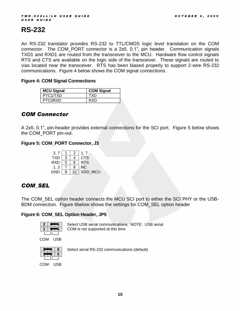
COM_SEL
The COM_SEL option header connects the MCU SCI port to either the SCI PHY or the USB-BDM connection. Figure 6below shows the settings for COM_SEL option header
Figure 6: COM_SEL Option Header, JP5
2 4 6 Select USB serial communications. NOTE: USB serial COM is not supported at this time 1 3 5
2 4 6 Select serial RS-232 communications (default) 1 3 5
COM USB
COM USB

T W R - S 0 8 L L / L H U S E R G U I D E O C T O B E R 6 , 2 0 0 9
U S E R G U I D E
11
LCD
The TWR-S08 applies a GD-5306P, 2x28 chip-on-glass, LCD connected directly to the target MCU. The target MCU provides the internal charge-pump and regulated LCD reference voltage required by the LCD. LCD contrast is trimmable under MCU control. Refer to the target device RM for further details on configuring using the LCD interface. The GD-5306P datasheet may be found on the Support CD included with the board. The LCD datasheet may also be found at www.axman.com/support.
ACCELEROMETER
The TWR-S08 applies the MMA7361L, 3-axis, analog accelerometer for tilt and motion-sense applications. The accelerometer supports 2 user selectable sensitivities - 1.5g / 6g. The SLEEP* input allows the device to be placed in a low-power mode. Separate X-, Y-, and Z-axis readings are routed to the MCU. Output filtering is applied to remove fast transients.
Configuration
Accelerometer sensitivity configuration is controlled manually using option select header JP2. The SLEEP* input is configurable manually or under MCU control. Figure 7 below shows the setting to configure the accelerometer output.
Figure 7: Accelerometer Sensitivity Select , JP6
Shunt
JP6 On Off
3 ▪ ▪ Accel in SLEEP mode Disabled (*)
2 ▪ ▪ Enable PTB5 control to Accel(*) Disabled
1 ▪ ▪ Selects ±6g Sensitivity Disabled(*) (*) – Default position
Cut-traces on the accelerometer output signals allow the user to disconnect the accelerometer output if necessary. Once cut, simply install a 1206 sized, 0-ohm resistor to reconnect the accelerometer output. Figure 8 below shows how the accelerometer output connects to the target MCU.
Figure 8: Accelerometer Output Cut-Traces
Signal Cut-Trace
MCU Input
X CT2 PTA1/ADP5
Y CT3 PTA2/ADP6
Z CT4 PTA3/ADP7
T W R - S 0 8 L L / L H U S E R G U I D E O C T O B E R 6 , 2 0 0 9
U S E R G U I D E
12
USER I/O
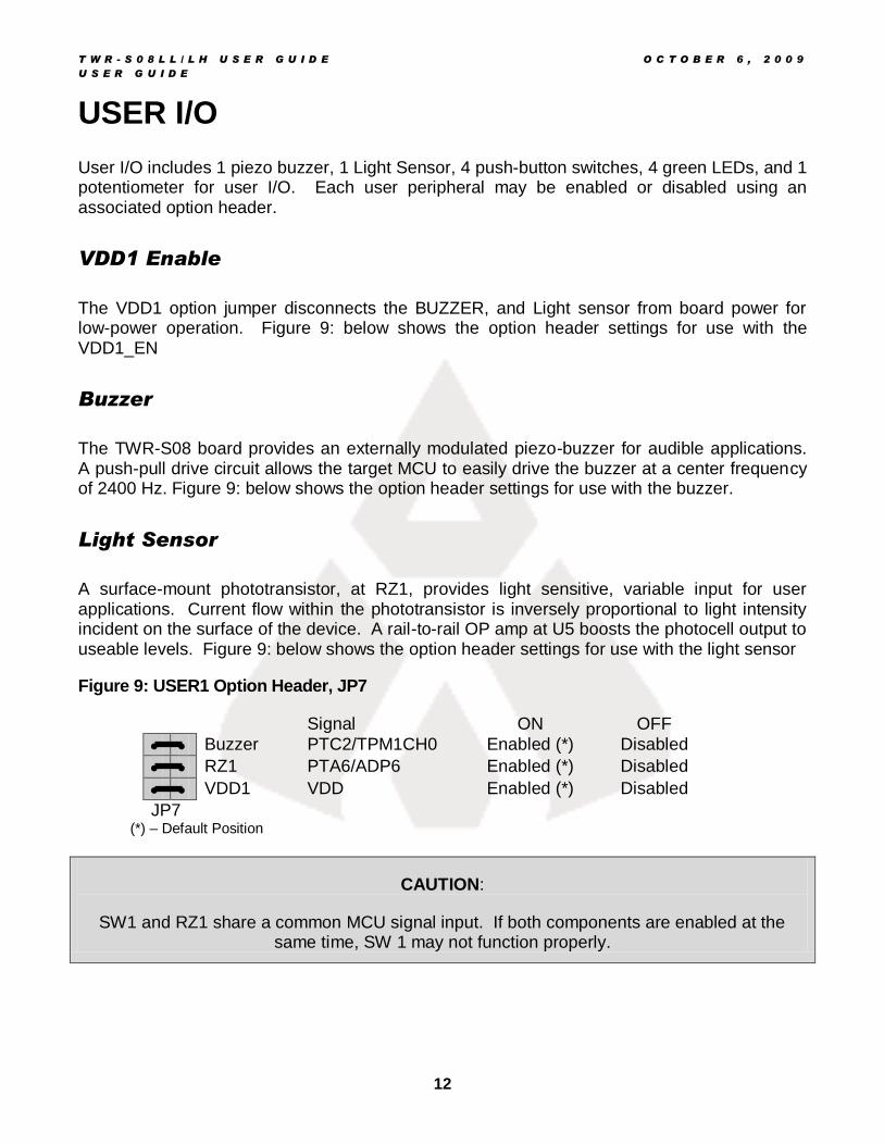
User I/O includes 1 piezo buzzer, 1 Light Sensor, 4 push-button switches, 4 green LEDs, and 1 potentiometer for user I/O. Each user peripheral may be enabled or disabled using an associated option header.
VDD1 Enable
The VDD1 option jumper disconnects the BUZZER, and Light sensor from board power for low-power operation. Figure 9: below shows the option header settings for use with the VDD1_EN
Buzzer
The TWR-S08 board provides an externally modulated piezo-buzzer for audible applications. A push-pull drive circuit allows the target MCU to easily drive the buzzer at a center frequency of 2400 Hz. Figure 9: below shows the option header settings for use with the buzzer.
Light Sensor
A surface-mount phototransistor, at RZ1, provides light sensitive, variable input for user applications. Current flow within the phototransistor is inversely proportional to light intensity incident on the surface of the device. A rail-to-rail OP amp at U5 boosts the photocell output to useable levels. Figure 9: below shows the option header settings for use with the light sensor
Figure 9: USER1 Option Header, JP7
Signal ON OFF
Buzzer PTC2/TPM1CH0 Enabled (*) Disabled
RZ1 PTA6/ADP6 Enabled (*) Disabled
VDD1 VDD Enabled (*) Disabled
JP7 (*) – Default Position
CAUTION:
SW1 and RZ1 share a common MCU signal input. If both components are enabled at the same time, SW 1 may not function properly.
T W R - S 0 8 L L / L H U S E R G U I D E O C T O B E R 6 , 2 0 0 9
U S E R G U I D E
13
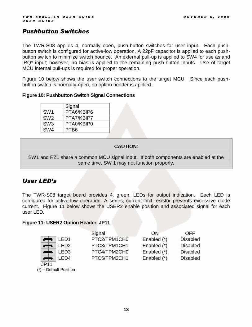
Pushbutton Switches
The TWR-S08 applies 4, normally open, push-button switches for user input. Each push-button switch is configured for active-low operation. A 22pF capacitor is applied to each push-button switch to minimize switch bounce. An external pull-up is applied to SW4 for use as and IRQ* input; however, no bias is applied to the remaining push-button inputs. Use of target MCU internal pull-ups is required for proper operation.
Figure 10 below shows the user switch connections to the target MCU. Since each push-button switch is normally-open, no option header is applied.
Figure 10: Pushbutton Switch Signal Connections
Signal
SW1 PTA6/KBIP6
SW2 PTA7/KBIP7
SW3 PTA0/KBIP0
SW4 PTB6
CAUTION:
SW1 and RZ1 share a common MCU signal input. If both components are enabled at the same time, SW 1 may not function properly.
User LED’s
The TWR-S08 target board provides 4, green, LEDs for output indication. Each LED is configured for active-low operation. A series, current-limit resistor prevents excessive diode current. Figure 11 below shows the USER2 enable position and associated signal for each user LED.
Figure 11: USER2 Option Header, JP11
Signal ON OFF
LED1 PTC2/TPM1CH0 Enabled (*) Disabled
LED2 PTC3/TPM1CH1 Enabled (*) Disabled
LED3 PTC4/TPM2CH0 Enabled (*) Disabled
LED4 PTC5/TPM2CH1 Enabled (*) Disabled
JP11 (*) – Default Position
T W R - S 0 8 L L / L H U S E R G U I D E O C T O B E R 6 , 2 0 0 9
U S E R G U I D E
14
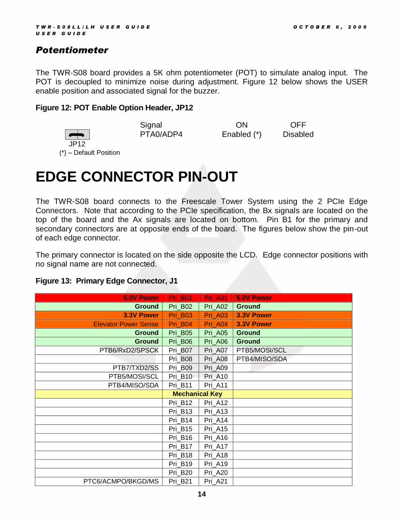
Potentiometer
The TWR-S08 board provides a 5K ohm potentiometer (POT) to simulate analog input. The POT is decoupled to minimize noise during adjustment. Figure 12 below shows the USER enable position and associated signal for the buzzer.
Figure 12: POT Enable Option Header, JP12
Signal ON OFF
PTA0/ADP4 Enabled (*) Disabled
JP12 (*) – Default Position
EDGE CONNECTOR PIN-OUT
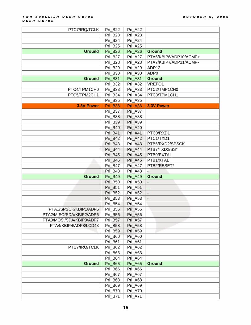
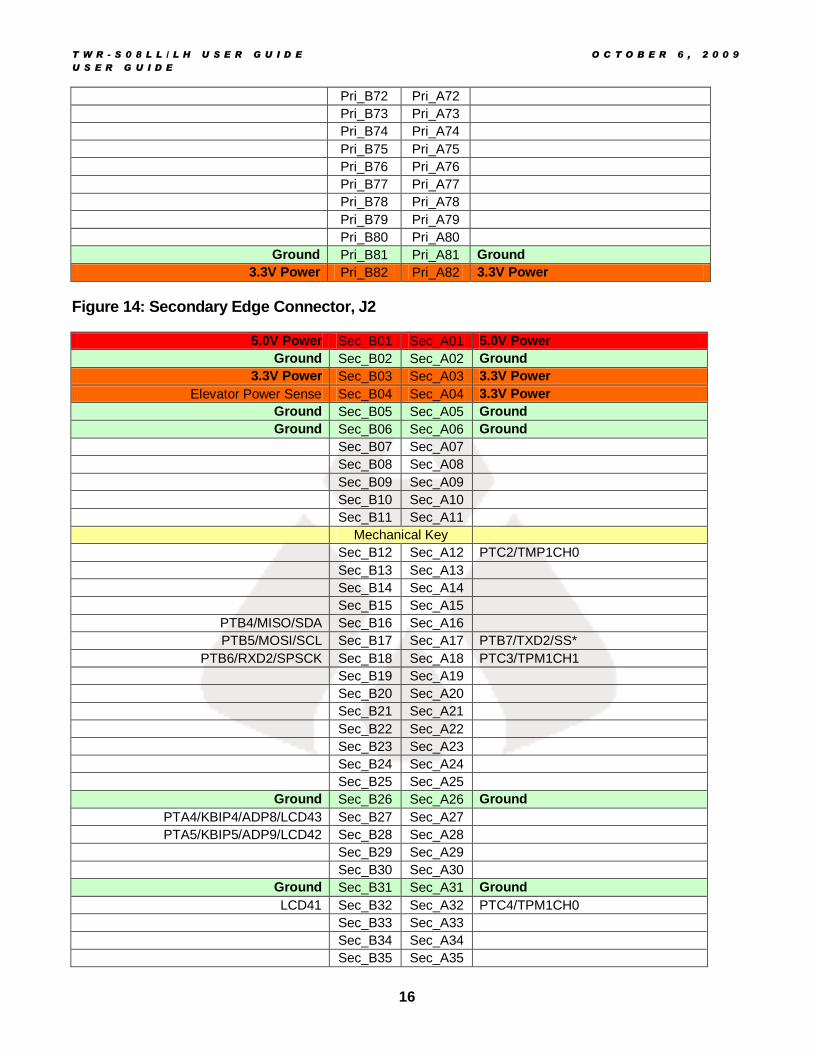
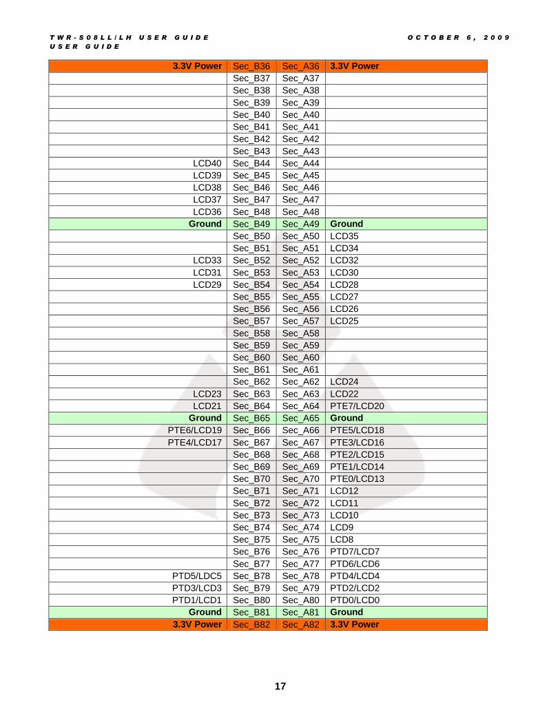
The TWR-S08 board connects to the Freescale Tower System using the 2 PCIe Edge Connectors. Note that according to the PCIe specification, the Bx signals are located on the top of the board and the Ax signals are located on bottom. Pin B1 for the primary and secondary connectors are at opposite ends of the board. The figures below show the pin-out of each edge connector.
The primary connector is located on the side opposite the LCD. Edge connector positions with no signal name are not connected.
Figure 13: Primary Edge Connector, J1
5.0V Power Pri_B01 Pri_A01 5.0V Power
Ground Pri_B02 Pri_A02 Ground
3.3V Power Pri_B03 Pri_A03 3.3V Power
Elevator Power Sense Pri_B04 Pri_A04 3.3V Power
Ground Pri_B05 Pri_A05 Ground
Ground Pri_B06 Pri_A06 Ground
PTB6/RxD2/SPSCK Pri_B07 Pri_A07 PTB5/MOSI/SCL
Pri_B08 Pri_A08 PTB4/MISO/SDA
PTB7/TXD2/SS Pri_B09 Pri_A09
PTB5/MOSI/SCL Pri_B10 Pri_A10
PTB4/MISO/SDA Pri_B11 Pri_A11
Mechanical Key
Pri_B12 Pri_A12
Pri_B13 Pri_A13
Pri_B14 Pri_A14
Pri_B15 Pri_A15
Pri_B16 Pri_A16
Pri_B17 Pri_A17
Pri_B18 Pri_A18
Pri_B19 Pri_A19
Pri_B20 Pri_A20
PTC6/ACMPO/BKGD/MS Pri_B21 Pri_A21
T W R - S 0 8 L L / L H U S E R G U I D E O C T O B E R 6 , 2 0 0 9
U S E R G U I D E
15
PTC7/IRQ/TCLK Pri_B22 Pri_A22
Pri_B23 Pri_A23
Pri_B24 Pri_A24
Pri_B25 Pri_A25
Ground Pri_B26 Pri_A26 Ground
Pri_B27 Pri_A27 PTA6/KBIP6/ADP10/ACMP+
Pri_B28 Pri_A28 PTA7/KBIP7/ADP11/ACMP-
Pri_B29 Pri_A29 ADP12
Pri_B30 Pri_A30 ADP0
Ground Pri_B31 Pri_A31 Ground
Pri_B32 Pri_A32 VREFO1
PTC4/TPM1CH0 Pri_B33 Pri_A33 PTC2/TMP1CH0
PTC5/TPM2CH1 Pri_B34 Pri_A34 PTC3/TPM1CH1
Pri_B35 Pri_A35
3.3V Power Pri_B36 Pri_A36 3.3V Power
Pri_B37 Pri_A37
Pri_B38 Pri_A38
Pri_B39 Pri_A39
Pri_B40 Pri_A40
Pri_B41 Pri_A41 PTC0/RXD1
Pri_B42 Pri_A42 PTC1/TXD1
Pri_B43 Pri_A43 PTB6/RXD2/SPSCK
Pri_B44 Pri_A44 PTB7/TXD2/SS*
Pri_B45 Pri_A45 PTB0/EXTAL
Pri_B46 Pri_A46 PTB1/XTAL
Pri_B47 Pri_A47 PTB2/RESET*
Pri_B48 Pri_A48
Ground Pri_B49 Pri_A49 Ground
Pri_B50 Pri_A50
Pri_B51 Pri_A51
Pri_B52 Pri_A52
Pri_B53 Pri_A53
Pri_B54 Pri_A54
PTA1/SPSCK/KBIP1/ADP5 Pri_B55 Pri_A55
PTA2/MISO/SDA/KBIP2/ADP6 Pri_B56 Pri_A56
PTA3/MOSI/SDA/KBIP3/ADP7 Pri_B57 Pri_A57
PTA4/KBIP4/ADP8/LCD43 Pri_B58 Pri_A58
Pri_B59 Pri_A59
Pri_B60 Pri_A60
Pri_B61 Pri_A61
PTC7/IRQ/TCLK Pri_B62 Pri_A62
Pri_B63 Pri_A63
Pri_B64 Pri_A64
Ground Pri_B65 Pri_A65 Ground
Pri_B66 Pri_A66
Pri_B67 Pri_A67
Pri_B68 Pri_A68
Pri_B69 Pri_A69
Pri_B70 Pri_A70
Pri_B71 Pri_A71
T W R - S 0 8 L L / L H U S E R G U I D E O C T O B E R 6 , 2 0 0 9
U S E R G U I D E
16
Pri_B72 Pri_A72
Pri_B73 Pri_A73
Pri_B74 Pri_A74
Pri_B75 Pri_A75
Pri_B76 Pri_A76
Pri_B77 Pri_A77
Pri_B78 Pri_A78
Pri_B79 Pri_A79
Pri_B80 Pri_A80
Ground Pri_B81 Pri_A81 Ground
3.3V Power Pri_B82 Pri_A82 3.3V Power
Figure 14: Secondary Edge Connector, J2
5.0V Power Sec_B01 Sec_A01 5.0V Power
Ground Sec_B02 Sec_A02 Ground
3.3V Power Sec_B03 Sec_A03 3.3V Power
Elevator Power Sense Sec_B04 Sec_A04 3.3V Power
Ground Sec_B05 Sec_A05 Ground
Ground Sec_B06 Sec_A06 Ground
Sec_B07 Sec_A07
Sec_B08 Sec_A08
Sec_B09 Sec_A09
Sec_B10 Sec_A10
Sec_B11 Sec_A11
Mechanical Key
Sec_B12 Sec_A12 PTC2/TMP1CH0
Sec_B13 Sec_A13
Sec_B14 Sec_A14
Sec_B15 Sec_A15
PTB4/MISO/SDA Sec_B16 Sec_A16
PTB5/MOSI/SCL Sec_B17 Sec_A17 PTB7/TXD2/SS*
PTB6/RXD2/SPSCK Sec_B18 Sec_A18 PTC3/TPM1CH1
Sec_B19 Sec_A19
Sec_B20 Sec_A20
Sec_B21 Sec_A21
Sec_B22 Sec_A22
Sec_B23 Sec_A23
Sec_B24 Sec_A24
Sec_B25 Sec_A25
Ground Sec_B26 Sec_A26 Ground
PTA4/KBIP4/ADP8/LCD43 Sec_B27 Sec_A27
PTA5/KBIP5/ADP9/LCD42 Sec_B28 Sec_A28
Sec_B29 Sec_A29
Sec_B30 Sec_A30
Ground Sec_B31 Sec_A31 Ground
LCD41 Sec_B32 Sec_A32 PTC4/TPM1CH0
Sec_B33 Sec_A33
Sec_B34 Sec_A34
Sec_B35 Sec_A35
T W R - S 0 8 L L / L H U S E R G U I D E O C T O B E R 6 , 2 0 0 9
U S E R G U I D E
17
3.3V Power Sec_B36 Sec_A36 3.3V Power
Sec_B37 Sec_A37
Sec_B38 Sec_A38
Sec_B39 Sec_A39
Sec_B40 Sec_A40
Sec_B41 Sec_A41
Sec_B42 Sec_A42
Sec_B43 Sec_A43
LCD40 Sec_B44 Sec_A44
LCD39 Sec_B45 Sec_A45
LCD38 Sec_B46 Sec_A46
LCD37 Sec_B47 Sec_A47
LCD36 Sec_B48 Sec_A48
Ground Sec_B49 Sec_A49 Ground
Sec_B50 Sec_A50 LCD35
Sec_B51 Sec_A51 LCD34
LCD33 Sec_B52 Sec_A52 LCD32
LCD31 Sec_B53 Sec_A53 LCD30
LCD29 Sec_B54 Sec_A54 LCD28
Sec_B55 Sec_A55 LCD27
Sec_B56 Sec_A56 LCD26
Sec_B57 Sec_A57 LCD25
Sec_B58 Sec_A58
Sec_B59 Sec_A59
Sec_B60 Sec_A60
Sec_B61 Sec_A61
Sec_B62 Sec_A62 LCD24
LCD23 Sec_B63 Sec_A63 LCD22
LCD21 Sec_B64 Sec_A64 PTE7/LCD20
Ground Sec_B65 Sec_A65 Ground
PTE6/LCD19 Sec_B66 Sec_A66 PTE5/LCD18
PTE4/LCD17 Sec_B67 Sec_A67 PTE3/LCD16
Sec_B68 Sec_A68 PTE2/LCD15
Sec_B69 Sec_A69 PTE1/LCD14
Sec_B70 Sec_A70 PTE0/LCD13
Sec_B71 Sec_A71 LCD12
Sec_B72 Sec_A72 LCD11
Sec_B73 Sec_A73 LCD10
Sec_B74 Sec_A74 LCD9
Sec_B75 Sec_A75 LCD8
Sec_B76 Sec_A76 PTD7/LCD7
Sec_B77 Sec_A77 PTD6/LCD6
PTD5/LDC5 Sec_B78 Sec_A78 PTD4/LCD4
PTD3/LCD3 Sec_B79 Sec_A79 PTD2/LCD2
PTD1/LCD1 Sec_B80 Sec_A80 PTD0/LCD0
Ground Sec_B81 Sec_A81 Ground
3.3V Power Sec_B82 Sec_A82 3.3V Power