transient clustering of reaction intermediates during … · transient clustering of reaction...
TRANSCRIPT
Transient Clustering of Reaction Intermediates during Wet Etching ofSilicon NanostructuresZainul Aabdin,†,‡,§,∥ Xiu Mei Xu,⊥ Soumyo Sen,# Utkarsh Anand,†,‡,§,∥ Petr Kral,#,∇,● Frank Holsteyns,⊥
and Utkur Mirsaidov*,†,‡,§,∥
†Department of Physics, National University of Singapore, 117551, Singapore‡Centre for BioImaging Sciences and Department of Biological Sciences, National University of Singapore, 117557, Singapore§Centre for Advanced 2D Materials and Graphene Research Centre, National University of Singapore, 117546, Singapore∥NUSNNI-NanoCore, National University of Singapore, 117411, Singapore⊥imec, Kapeldreef 75, Leuven, B-3001, Belgium#Department of Chemistry, ∇Department of Physics, University of Illinois at Chicago, Chicago, Illinois 60607, United States●Department of Biopharmaceutical Sciences, University of Illinois at Chicago, Chicago, Illinois 60612, United States
*S Supporting Information
ABSTRACT: Wet chemical etching is a key process infabricating silicon (Si) nanostructures. Currently, wet etchingof Si is proposed to occur through the reaction of surface Siatoms with etchant molecules, forming etch intermediates thatdissolve directly into the bulk etchant solution. Here, using insitu transmission electron microscopy (TEM), we follow thenanoscale wet etch dynamics of amorphous Si (a-Si)nanopillars in real-time and show that intermediates generatedduring alkaline wet etching first aggregate as nanoclusters onthe Si surface and then detach from the surface beforedissolving in the etchant solution. Molecular dynamicssimulations reveal that the molecules of etch intermediates remain weakly bound to the hydroxylated Si surface during theetching and aggregate into nanoclusters via surface diffusion instead of directly diffusing into the etchant solution. We confirmedthis model experimentally by suppressing the formation of nanoclusters of etch intermediates on the Si surfaces by shielding thehydroxylated Si sites with large ions. These results suggest that the interaction of etch intermediates with etching surfacescontrols the solubility of reaction intermediates and is an important parameter in fabricating densely packed clean 3Dnanostructures for future generation microelectronics.
KEYWORDS: Nanofabrication, nanopillars, nanowires, silicon, chemical etching, reaction intermediates,in situ transmission electron microscopy (TEM), liquid cell
The continuing drive for faster and more energy-efficientmicroelectronic components requires the fabrication of
smaller, denser, and better-defined nanostructures. For current-generation devices based on planar 2D layouts, the increase indevice density is achieved by reducing their planar sizes.However, with some current features already several tens ofatoms wide, following Moore’s law has become extremelychallenging.1,2 Therefore, the newest and future generations ofdevices are based on 3D nanodevice architectures.3 Forexample, the latest generation gate-all-around field effecttransistors are now incorporating vertical semiconductornanowires or nanopillars, which serve as channels for chargecarriers; the carrier flow is controlled by metal gates that wraparound these vertical channels.2,4,5 Vertical nanowires are alsofinding applications in solar cells,6 lasers,7 photodetectors,8 andnanoelectromechanical systems.9
However, fabricating 3D semiconductor nanostructures, forexample, nanowires, by present methods such as vapor−liquid−solid (VLS) mechanism based growth using catalysts seeded onsubstrates10,11 or dry plasma etching of bulk semiconductors12
poses challenges not faced with simpler 2D designs. As theaspect ratio and density of vertical nanowires increase with eachdevice generation, significant difficulties emerge in producingan ordered array of smaller diameter nanowires using the VLSmethod,13 while dry etching methods lead to plasma-induceddamage to the semiconductor surface. These surface defectsdrastically reduce the mobility of charge carriers and thusdegrade device performance and reliability.14 In contrast,chemical wet etching (post VLS growth or dry-etching) can
Received: January 16, 2017Revised: April 7, 2017Published: April 18, 2017
Letter
pubs.acs.org/NanoLett
© 2017 American Chemical Society 2953 DOI: 10.1021/acs.nanolett.7b00196Nano Lett. 2017, 17, 2953−2958
be tuned to produce small diameter nanostructures withdamage-free surfaces.15 Moreover, the high selectivity of wetetching processes for different materials or semiconductordoping levels enables more control over the geometry ofnanowires.16
Despite the technological importance of chemical wetetching in semiconductor micro- and nanofabrication, ourunderstanding of wet etching dynamics at the nanoscale isinferred from studies in bulk etching conditions. Etching is acomplex process that involves the formation of intermediatesthat are then transformed into soluble molecules. However, it isnot clear how these reaction intermediates are removed fromthe etching surfaces by etchant solutions.17,18 The accumulationof unwanted byproducts on the etching surfaces during wet ordry etching may lead to increased surface roughness andnonuniformities19 that can diminish the performance andreliability of fabricated nanodevices.20,21 Current methods areunable to monitor the wet etching processes in real-time at thenanoscale level.To understand wet etching dynamics at the nanoscale level,
we have taken a direct approach of imaging these intermediatesteps by in situ transmission electron microscopy (TEM).22,23
We can directly watch the thinning of densely packedamorphous Si (a-Si) nanopillars during etching in an aqueouspotassium hydroxide (KOH) solutiona widely used etchantin Si microfabrication.24−26 Contrary to our expectations, ourobservations reveal that nanoclusters of etch intermediates formand grow on the Si surface during wet etching. Theseintermediates later detach and dissolve in the etchant solution.A periodic array of free-standing a-Si nanopillars used in our
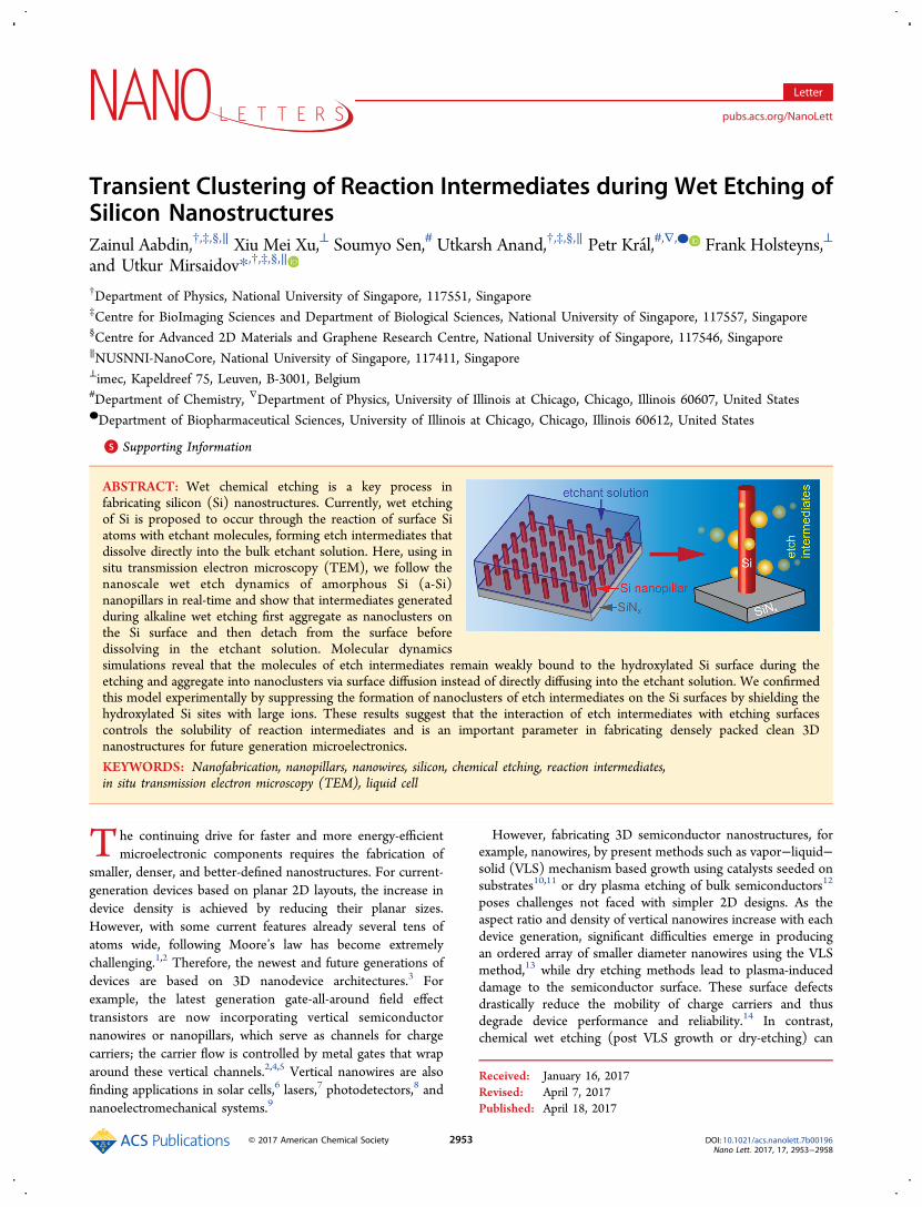
experiments is fabricated on a SiNx membrane (Figure 1B−C)and assembled into a liquid cell (Figure 1A) with a topelectron-translucent SiNx window separated by a spacer (SISections 1−2). The nanopillars are etched by a KOH solutionat room temperature and imaged at a rate of 10 frames persecond in the TEM at 200 kV and at a low electron flux of 5−25 e/(Å2·s), which has a negligible effect on the observedetching dynamics (SI Sections 7−9, 18).Real-time observations (Figure 2A−B and Figure 3A−C)
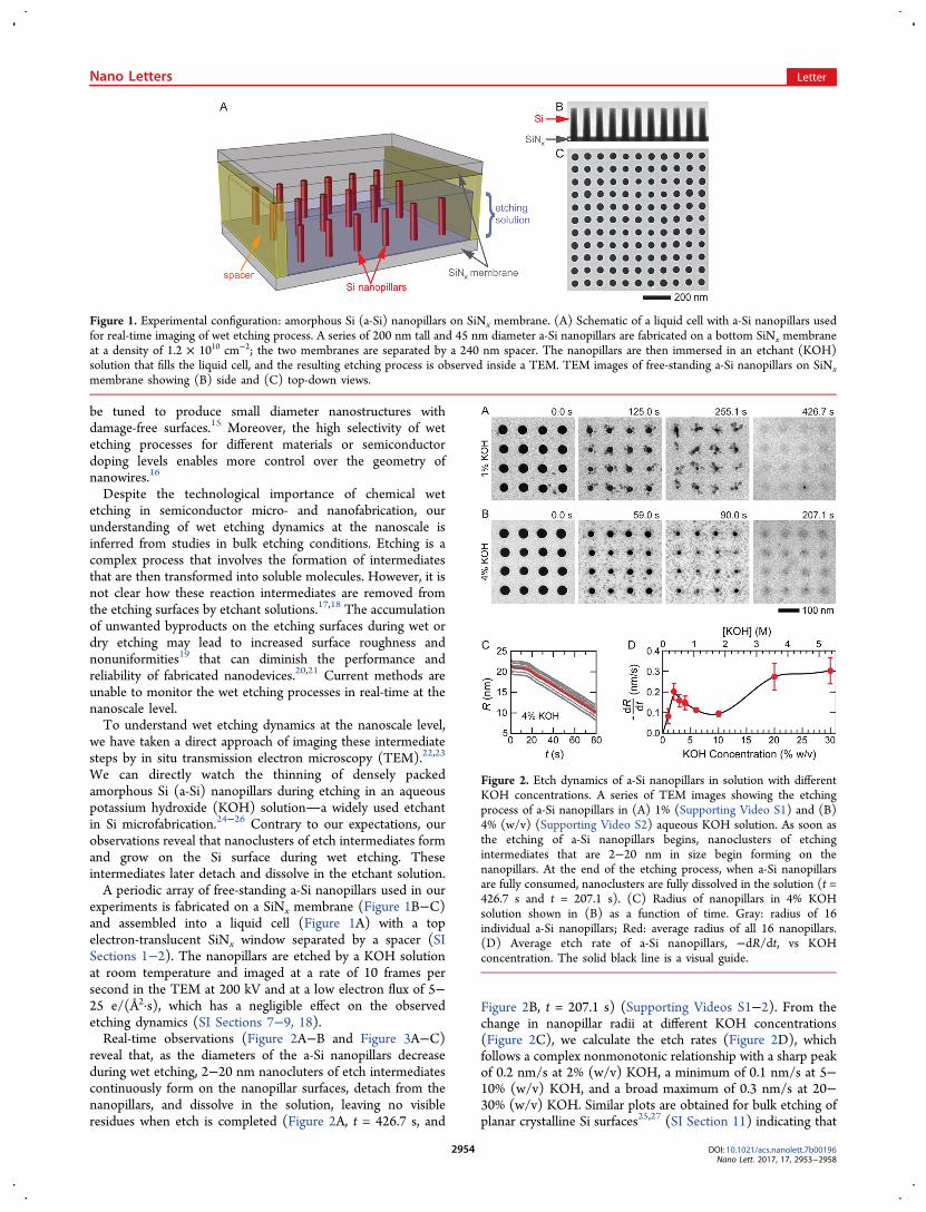
reveal that, as the diameters of the a-Si nanopillars decreaseduring wet etching, 2−20 nm nanocluters of etch intermediatescontinuously form on the nanopillar surfaces, detach from thenanopillars, and dissolve in the solution, leaving no visibleresidues when etch is completed (Figure 2A, t = 426.7 s, and
Figure 2B, t = 207.1 s) (Supporting Videos S1−2). From thechange in nanopillar radii at different KOH concentrations(Figure 2C), we calculate the etch rates (Figure 2D), whichfollows a complex nonmonotonic relationship with a sharp peakof 0.2 nm/s at 2% (w/v) KOH, a minimum of 0.1 nm/s at 5−10% (w/v) KOH, and a broad maximum of 0.3 nm/s at 20−30% (w/v) KOH. Similar plots are obtained for bulk etching ofplanar crystalline Si surfaces25,27 (SI Section 11) indicating that
Figure 1. Experimental configuration: amorphous Si (a-Si) nanopillars on SiNx membrane. (A) Schematic of a liquid cell with a-Si nanopillars usedfor real-time imaging of wet etching process. A series of 200 nm tall and 45 nm diameter a-Si nanopillars are fabricated on a bottom SiNx membraneat a density of 1.2 × 1010 cm−2; the two membranes are separated by a 240 nm spacer. The nanopillars are then immersed in an etchant (KOH)solution that fills the liquid cell, and the resulting etching process is observed inside a TEM. TEM images of free-standing a-Si nanopillars on SiNxmembrane showing (B) side and (C) top-down views.
Figure 2. Etch dynamics of a-Si nanopillars in solution with differentKOH concentrations. A series of TEM images showing the etchingprocess of a-Si nanopillars in (A) 1% (Supporting Video S1) and (B)4% (w/v) (Supporting Video S2) aqueous KOH solution. As soon asthe etching of a-Si nanopillars begins, nanoclusters of etchingintermediates that are 2−20 nm in size begin forming on thenanopillars. At the end of the etching process, when a-Si nanopillarsare fully consumed, nanoclusters are fully dissolved in the solution (t =426.7 s and t = 207.1 s). (C) Radius of nanopillars in 4% KOHsolution shown in (B) as a function of time. Gray: radius of 16individual a-Si nanopillars; Red: average radius of all 16 nanopillars.(D) Average etch rate of a-Si nanopillars, −dR/dt, vs KOHconcentration. The solid black line is a visual guide.
Nano Letters Letter
DOI: 10.1021/acs.nanolett.7b00196Nano Lett. 2017, 17, 2953−2958
2954
the underlying mechanisms at the nanoscale and bulk scale aresimilar.The transient clustering of etch intermediates, not reported
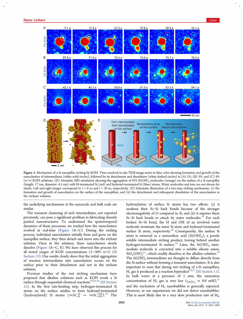
previously, can pose a significant problem in fabricating denselypacked nanostructures. To understand the spatiotemporaldynamics of these processes, we tracked how the nanoclustersevolved in real-time (Figure 3A−C). During the etchingprocess, individual nanoclusters initially form and grow on thenanopillar surface; they then detach and move into the etchantsolution. Once in the solution, these nanoclusters slowlydissolve (Figure 3A−C, E). We have observed this process forall tested ranges of KOH concentrations (1−30% w/v) (SISection 13). Our results clearly show that the initial aggregationof reaction intermediates into nanoclusters occurs on thesurface prior to their detachment and not in the etchantsolution.Previous studies of the wet etching mechanism have
proposed that alkaline solutions such as KOH erode a Sisurface through sequential chemical reactions24,25,28 (SI Section11). In the first rate-limiting step, hydrogen-terminated Siatoms on the surface oxidize to form hydroxyl-terminated(hydroxylated) Si atoms (Si−H
−H → Si−OH−OH).29 The
hydroxylation of surface Si atoms has two effects: (i) itweakens their Si−Si back bonds because of the strongerelectronegativity of O compared to Si, and (ii) it exposes theseSi−Si back bonds to attack by water molecules.30 For eachbroken Si−Si bond, the H and OH of an involved watermolecule terminate the inner Si atom and hydroxyl-terminatedsurface Si atom, respectively.30 Consequently, the surface Siatom is removed as a monosilicic acid (Si(OH)4), a poorlysoluble intermediate etching product, leaving behind anotherhydrogen-terminated Si surface.28 Later, the Si(OH)4 inter-mediate molecule is converted into a soluble silicate anion,SiO2(OH)2
2−, which readily dissolves in the alkaline solution.24
The Si(OH)4 intermediates are thought to diffuse directly fromthe Si surface without forming a transient nanoclusters. It is alsoimportant to note that during wet etching of a-Si nanopillars,H2 gas is produced as a reaction byproduct24,27 (SI Section 11).In bulk water at a pressure of 1 atm, the saturationconcentration of H2 gas is very low (csat(H2) ≈ 0.8 mM),31
and the nucleation of H2 nanobubbles is generally expected.However, in our experiments we did not detect nanobubbles.This is most likely due to a very slow production rate of H2,
Figure 3.Mechanism of a-Si nanopillar etching by KOH. Time-resolved in situ TEM image series in false color showing formation and growth of thenanoclusters of intermediates (white solid circles), followed by its detachment and dissolution (white dashed circles) in (A) 1%, (B) 3%, and (C) 4%(w/v) KOH solutions. (D) Atomistic MD simulation showing the aggregation of 935 Si(OH)4 molecules (orange) on the surface of a Si nanopillar(length: 17 nm, diameter: 4.5 nm) with H-terminated Si (red) and hydroxyl-terminated Si (blue) atoms. Water molecules and ions are not shown forclarity. Left and right images correspond to t = 0 ns and t = 30 ns, respectively. (E) Schematic illustration of a two-step etching mechanism: (i) theformation and growth of nanoclusters on the surface of the nanopillars, and (ii) the detachment and subsequent dissolution of the nanoclusters inthe etchant solution.
Nano Letters Letter
DOI: 10.1021/acs.nanolett.7b00196Nano Lett. 2017, 17, 2953−2958
2955
owing to slow Si etch rates at room temperature, and fastupward diffusion of H2 into air gaps in the loading pockets ofour liquid cells (Figure 1 and Figure S1).Given this multistep dynamics of Si wet etching, it is
important to clarify the nature of the nanoclusters formed on Sisurfaces during their etching. We hypothesize that theintermediate molecules (Si(OH)4) cluster on the Si surfacebefore being converted into soluble silicate anions(SiO2(OH)2
2−). To check this hypothesis, we modeled thedynamics of Si(OH)4 intermediates on wet etched Si surface byatomistic molecular dynamics (MD) simulations. Initially,Si(OH)4 molecules were uniformly distributed on the hydro-gen- and hydroxyl-terminated surface of the Si nanopillar(Figure 3D) (SI Section 17). The simulations show thatSi(OH)4 intermediate products reorganize on the nanopillarsurface into small nanoclusters instead of moving into solution(Figure 3D). The neighboring nanoclusters further aggregateinto larger surface-bound clusters that closely resemble thenanoclusters that we imaged in our in situ TEM experiments(Figure 3A−C). The Si(OH)4 clusters are held on the Sinanopillar surface, with less than ∼3% of the Si(OH)4intermediates escaping into the solution during the simulation.The model confirms that the hydroxylated Si surface weakly
attracts the intermediate Si(OH)4 molecules and their clusters.The aggregation of Si(OH)4 intermediates into nanoclusters isconsistent with the strong hydrogen bonding between theseintermediates32,33 (SI Section 17, Figure S20). Small amountsof other silicate species that form as a result of theoligomerization of silicic acid molecules can also participateas intermediate products34,35 (SI Section 12) and be potentiallypresent within the experimentally observed intermediatenanoclusters. Nevertheless, throughout the entire etchingprocess and regardless of the composition of the nanoclusters,these etching intermediates are transported from the surfaceinto the etchant solution in the form of nanoclusters, wherethey dissolve.Our simulations also reveal that, in the absence of the
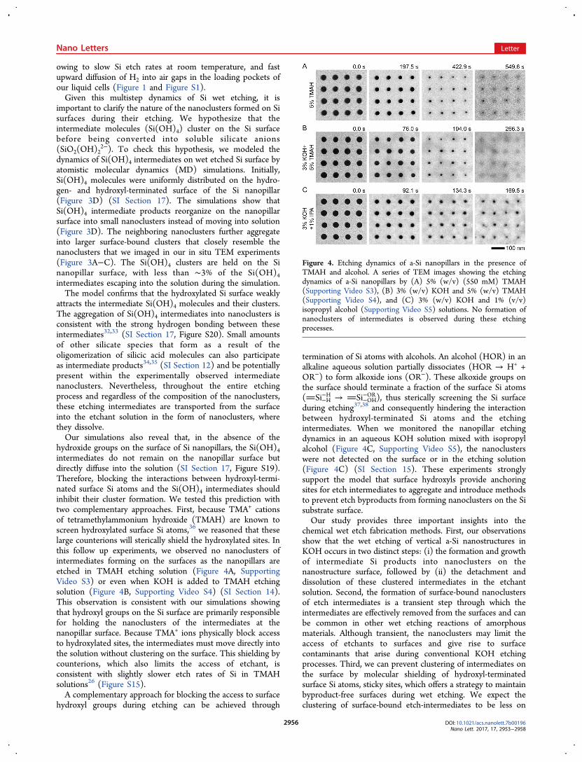
hydroxide groups on the surface of Si nanopillars, the Si(OH)4intermediates do not remain on the nanopillar surface butdirectly diffuse into the solution (SI Section 17, Figure S19).Therefore, blocking the interactions between hydroxyl-termi-nated surface Si atoms and the Si(OH)4 intermediates shouldinhibit their cluster formation. We tested this prediction withtwo complementary approaches. First, because TMA+ cationsof tetramethylammonium hydroxide (TMAH) are known toscreen hydroxylated surface Si atoms,36 we reasoned that theselarge counterions will sterically shield the hydroxylated sites. Inthis follow up experiments, we observed no nanoclusters ofintermediates forming on the surfaces as the nanopillars areetched in TMAH etching solution (Figure 4A, SupportingVideo S3) or even when KOH is added to TMAH etchingsolution (Figure 4B, Supporting Video S4) (SI Section 14).This observation is consistent with our simulations showingthat hydroxyl groups on the Si surface are primarily responsiblefor holding the nanoclusters of the intermediates at thenanopillar surface. Because TMA+ ions physically block accessto hydroxylated sites, the intermediates must move directly intothe solution without clustering on the surface. This shielding bycounterions, which also limits the access of etchant, isconsistent with slightly slower etch rates of Si in TMAHsolutions26 (Figure S15).A complementary approach for blocking the access to surface
hydroxyl groups during etching can be achieved through
termination of Si atoms with alcohols. An alcohol (HOR) in analkaline aqueous solution partially dissociates (HOR → H+ +OR−) to form alkoxide ions (OR−). These alkoxide groups onthe surface should terminate a fraction of the surface Si atoms(Si−H
−H → Si−OH−OR), thus sterically screening the Si surface
during etching37,38 and consequently hindering the interactionbetween hydroxyl-terminated Si atoms and the etchingintermediates. When we monitored the nanopillar etchingdynamics in an aqueous KOH solution mixed with isopropylalcohol (Figure 4C, Supporting Video S5), the nanoclusterswere not detected on the surface or in the etching solution(Figure 4C) (SI Section 15). These experiments stronglysupport the model that surface hydroxyls provide anchoringsites for etch intermediates to aggregate and introduce methodsto prevent etch byproducts from forming nanoclusters on the Sisubstrate surface.Our study provides three important insights into the
chemical wet etch fabrication methods. First, our observationsshow that the wet etching of vertical a-Si nanostructures inKOH occurs in two distinct steps: (i) the formation and growthof intermediate Si products into nanoclusters on thenanostructure surface, followed by (ii) the detachment anddissolution of these clustered intermediates in the etchantsolution. Second, the formation of surface-bound nanoclustersof etch intermediates is a transient step through which theintermediates are effectively removed from the surfaces and canbe common in other wet etching reactions of amorphousmaterials. Although transient, the nanoclusters may limit theaccess of etchants to surfaces and give rise to surfacecontaminants that arise during conventional KOH etchingprocesses. Third, we can prevent clustering of intermediates onthe surface by molecular shielding of hydroxyl-terminatedsurface Si atoms, sticky sites, which offers a strategy to maintainbyproduct-free surfaces during wet etching. We expect theclustering of surface-bound etch-intermediates to be less on
Figure 4. Etching dynamics of a-Si nanopillars in the presence ofTMAH and alcohol. A series of TEM images showing the etchingdynamics of a-Si nanopillars by (A) 5% (w/v) (550 mM) TMAH(Supporting Video S3), (B) 3% (w/v) KOH and 5% (w/v) TMAH(Supporting Video S4), and (C) 3% (w/v) KOH and 1% (v/v)isopropyl alcohol (Supporting Video S5) solutions. No formation ofnanoclusters of intermediates is observed during these etchingprocesses.
Nano Letters Letter
DOI: 10.1021/acs.nanolett.7b00196Nano Lett. 2017, 17, 2953−2958
2956
smooth surfaces of crystalline Si nanostructures, because thedensity of OH-terminated sites is higher on rough surfaces of a-Si structures. In general, the ability to observe and controletching processes at the nanoscale and in real-time by in situTEM will certainly improve the design of new top-downnanofabrication processes for next-generation nanoscaledevices.
■ ASSOCIATED CONTENT*S Supporting InformationThe Supporting Information is available free of charge on theACS Publications website at DOI: 10.1021/acs.nano-lett.7b00196.
Materials and methods, additional experiments, andrelevant discussions (PDF)Video S1. In situ TEM movie shows the etchingdynamics of Si nanopillars etched by 1% (w/v) aqueousKOH solution at 22 °C. As soon as etching of Sinanopillars begins, etch intermediates begin formingsmall nanoclusters on the surface of the nanopillars.Nanoclusters detach from the surface when they reachthe size of 2−20 nm. At the end of the etching process,when the nanopillars are fully consumed, all of thenanoclusters are fully dissolved in the KOH solution(Figure 2A) (AVI)Video S2. In situ TEM movie shows the etchingdynamics of Si nanopillars etched by 4% (w/v) aqueousKOH solution at 22 °C. Similar to the 1% (w/v) KOHconcentration, nanoclusters of etch intermediates formon the surface of the Si nanopillars during the etching(Figure 2B). Again, at the end of the etching process,nanoclusters are completely dissolved in the KOHsolution (AVI)Video S3. In situ TEM movie shows the etchingdynamics of Si nanopillars etched by 5% (w/v) aqueousTMAH solution at 22 °C. In contrast to KOH etching,no formation of nanoclusters of etch intermediates isobserved (Figure 4A) (AVI)Video S4. In situ TEM movie shows the etchingdynamics of Si nanopillars etched by 3% (w/v) aqueousKOH and 5% (w/v) TMAH solution mixture at 22 °C.Similar to TMAH etching, no formation of nanoclustersis observed (Figure 4B)(AVI)Video S5. In situ TEM movie shows the etchingdynamics of Si nanopillars etched by 3% (w/v) aqueousKOH and 1% (v/v) isopropyl alcohol solution mixture at22 °C. Similar to TMAH etching, no formation ofnanoclusters is observed (Figure 4C) (AVI)
■ AUTHOR INFORMATIONCorresponding Author*E-mail: [email protected] Kral: 0000-0003-2992-9027Utkur Mirsaidov: 0000-0001-8673-466XNotesThe authors declare no competing financial interest.
■ ACKNOWLEDGMENTSThis work was supported by the Singapore National ResearchFoundation’s Competitive Research Program funding (NRF-
CRP9-2011-04 and NRF-CRP16-2015-05) and the NUSYoung Investigator Award (NUSYIA-FY14-P17) from theNational University of Singapore. P.K. acknowledges supportobtained from the NSF DMR #1506886 award. We thankVasile Paraschiv, Guy Vereecke, and Harold Philipsen for theirsupport and discussions.
■ REFERENCES(1) Waldrop, M. M. Nature 2016, 530, 144−147.(2) Kuhn, K. IEEE Trans. Electron Devices 2012, 59, 1813−1828.(3) Thelander, C.; Agarwal, P.; Brongersma, S.; Eymery, J.; Feiner, L.F.; Forchel, A.; Scheffler, M.; Riess, W.; Ohlsson, B. J.; Gosele, U.;Samuelson, L. Mater. Today 2006, 9, 28−35.(4) Goldberger, J.; Hochbaum, A. I.; Fan, R.; Yang, P. Nano Lett.2006, 6, 973−977.(5) Tomioka, K.; Yoshimura, M.; Fukui, T. Nature 2012, 488, 189−192.(6) Kapadia, R.; Fan, Z.; Takei, K.; Javey, A. Nano Energy 2012, 1,132−144.(7) Huang, M. H.; Mao, S.; Feick, H.; Yan, H.; Wu, Y.; Kind, H.;Weber, E.; Russo, R.; Yang, P. Science 2001, 292, 1897−1899.(8) Yan, R.; Gargas, D.; Yang, P. Nat. Photonics 2009, 3, 569−576.(9) Craighead, H. G. Science 2000, 290, 1532−1535.(10) Hannon, J. B.; Kodambaka, S.; Ross, F. M.; Tromp, R. M.Nature 2006, 440, 69−71.(11) Panciera, F.; Chou, Y. C.; Reuter, M. C.; Zakharov, D.; Stach, E.A.; Hofmann, S.; Ross, F. M. Nat. Mater. 2015, 14, 820−825.(12) Donnelly, V. M.; Kornblit, A. J. Vac. Sci. Technol., A 2013, 31,050825.(13) Choi, H.-J. Semiconductor Nanostructures for OptoelectronicDevices; Springer: Berlin, 2012.(14) Shul, R. J.; Pearton, S. J. Handbook of advanced plasma processingtechniques; Springer Science & Business Media, 2011.(15) Pinion, C. W.; Christesen, J. D.; Cahoon, J. F. J. Mater. Chem. C2016, 4, 3890−3897.(16) Christesen, J. D.; Pinion, C. W.; Grumstrup, E. M.; Papanikolas,J. M.; Cahoon, J. F. Nano Lett. 2013, 13, 6281−6286.(17) Choppin, G. R.; Pathak, P.; Thakur, P. Main Group Met. Chem.2008, 31, 53−72.(18) Nijdam, A. J.; Veenendaal, E. v.; Gardeniers, J. G. E.; Kentgens,A. P. M.; Nachtegaal, G. H.; Elwenspoek, M. J. Electrochem. Soc. 2000,147, 2195−2198.(19) Song-Sheng, T.; Reed, M. L.; Hongtao, H.; Boudreau, R. J.Microelectromech. Syst. 1996, 5, 66−72.(20) Lee, J. W.; Jang, D.; Mouis, M.; Kim, G. T.; Chiarella, T.;Hoffmann, T.; Ghibaudo, G. Solid-State Electron. 2011, 62, 195−201.(21) Wang, F.; Yip, S.; Han, N.; Fok, K.; Lin, H.; Hou, J. J.; Dong, G.;Hung, T.; Chan, K. S.; Ho, J. C. Nanotechnology 2013, 24, 375202.(22) Zheng, H.; Smith, R. K.; Jun, Y.-w.; Kisielowski, C.; Dahmen,U.; Alivisatos, A. P. Science 2009, 324, 1309−1312.(23) Ross, F. M. Science 2015, 350, 9886.(24) Seidel, H.; Csepregi, L.; Heuberger, A.; Baumgartel, H. J.Electrochem. Soc. 1990, 137, 3612−3626.(25) Glembocki, O. J.; Palik, E. D.; Guel, G. R. d.; Kendall, D. L. J.Electrochem. Soc. 1991, 138, 1055−1063.(26) Shikida, M.; Sato, K.; Tokoro, K.; Uchikawa, D. Sens. Actuators,A 2000, 80, 179−188.(27) Palik, E. D.; Glembocki, O. J., Jr.; Burno, P. S.; Tenerz, L.;Heard, I. J. Appl. Phys. 1991, 70, 3291−3300.(28) Allongue, P. Phys. Rev. Lett. 1996, 77, 1986−1989.(29) Baum, T.; Schiffrin, D. J. J. Electroanal. Chem. 1997, 436, 239−244.(30) Gosalvez, M. A.; Zubel, I.; Viinikka, E. Chapter 22 - Wet Etchingof Silicon. In Handbook of Silicon Based MEMS Materials andTechnologies, 2nd ed.; William Andrew Publishing: Boston, 2015; pp470−502.(31) Sander, R. Atmos. Chem. Phys. 2015, 15, 4399−4981.
Nano Letters Letter
DOI: 10.1021/acs.nanolett.7b00196Nano Lett. 2017, 17, 2953−2958
2957
(32) Preari, M.; Spinde, K.; Lazic, J.; Brunner, E.; Demadis, K. D. J.Am. Chem. Soc. 2014, 136, 4236−4244.(33) Zeglinski, J.; Piotrowski, G. P.; Piękos, R. J. Mol. Struct. 2006,794, 83−91.(34) Michaud, P. T.; Babic, D. J. Electrochem. Soc. 1998, 145, 4040−4043.(35) Palik, E. D.; Gray, H. F.; Klein, P. B. J. Electrochem. Soc. 1983,130, 956−959.(36) Gosalvez, M. A.; Sato, K.; Foster, A. S.; Nieminen, R. M.;Tanaka, H. J. Micromech. Microeng. 2007, 17, S1−S26.(37) Bitzer, T.; Richardson, N. V.; Schiffrin, D. J. Surf. Sci. 1997, 382,L686−L689.(38) Newton, T. A.; Huang, Y.-C.; Lepak, L. A.; Hines, M. A. J. Chem.Phys. 1999, 111, 9125−9128.
Nano Letters Letter
DOI: 10.1021/acs.nanolett.7b00196Nano Lett. 2017, 17, 2953−2958
2958