thyristors and triacs
TRANSCRIPT
7/25/2019 Thyristors and Triacs
http://slidepdf.com/reader/full/thyristors-and-triacs 1/84
Thyristors and Triacs Power Semiconductor Applications Philips Semiconductors
CHAPTER 6
Power Control with Thyristors and Triacs
6.1 Using Thyristors and Triacs
6.2 Thyristor and Triac Applications
6.3 Hi-Com Triacs
485

7/25/2019 Thyristors and Triacs
http://slidepdf.com/reader/full/thyristors-and-triacs 2/84

7/25/2019 Thyristors and Triacs
http://slidepdf.com/reader/full/thyristors-and-triacs 3/84
Thyristors and Triacs Power Semiconductor Applications Philips Semiconductors
Using Thyristors and Triacs
487

7/25/2019 Thyristors and Triacs
http://slidepdf.com/reader/full/thyristors-and-triacs 4/84
7/25/2019 Thyristors and Triacs
http://slidepdf.com/reader/full/thyristors-and-triacs 5/84
Thyristors and Triacs Power Semiconductor Applications Philips Semiconductors
6.1.1 Introduction to Thyristors and Triacs
Brief summary of the thyristor family
The term thyristor is a generic name for a semiconductorswitch having four or more layers and is, in essence, ap-n-p-n sandwich. Thyristors form a large family and it ishelpful to consider the constituents which determine thetype of any given thyristor. If an ohmic connection is madeto the first p region and the last n region, and no otherconnection is made, the device is a diode thyristor. If anadditional ohmic connection is made to the intermediate nregion (n gate type) or the intermediate p region (p gatetype), thedevice is a triode thyristor. If an ohmic connectionismade toboth intermediateregions, thedevice isa tetrodethyristor. All such devices have a forward characteristic ofthe general form shown in Fig. 1.
There are three types of thyristor reverse characteristic:blocking (as in normal diodes), conducting (large reversecurrents at low reverse voltages) and approximate mirrorimageof theforward characteristic (bidirectional thyristors).Reverse blocking devices usually have four layers or lesswhereas reverse conducting and mirror image devicesusually have five layers.
The simplest thyristor structure, and the most common, isthe reverse blocking triode thyristor (usuallysimply referredto as the ’thyristor’ or SCR ’silicon controlled rectifier’). Itscircuit symbol and basic structure are shown in Fig. 2.
The most complex common thyristor structure is thebidirectional triode thyristor, or triac. The triac (shown inFig. 3) isable topass current bidirectionallyand is thereforean a.c. power control device. Its performance is that of apair of thyristors in anti-parallel with a single gate terminal.The triac needs only one heatsink, but this must be largeenough to remove the heat caused by bidirectional currentflow. Triac gate triggering circuits must be designed withcare to ensurethat unwantedconduction, ie. loss ofcontrol,does not occur when triggering lasts too long.
Thyristors and triacs are both bipolar devices. They havevery lowon-statevoltages but, because theminority chargecarriers in the devices must be removed before they can
block an applied voltage, the switching times arecomparatively long. This limits thyristorswitching circuits tolow frequency applications. Triacs are used almostexclusivelyatmainssupply frequenciesof50or60Hz,whilein some applications this extends up to the 400Hz supplyfrequency as used in aircraft.
Thevoltage blocking capabilitiesof thyristors and triacs arequite high: the highest voltage rating for the Philips rangeis 800V, while the currents (IT(RMS)) range from 0.8A to 25A.
The devices are available as surface mount components,
or as non-isolated or isolated discrete devices, dependingon the device rating.
Fig. 1 Thyristor static characteristic
Fig. 2 Thyristor circuit symbol and basic structure
Fig. 3 Triac circuit symbol and basic structure
On-statecharacteristic
Off-statecharacteristic
Avalanchebreakdownregion
Reversecharacteristic
Reversecurrent
Forwardcurrent
Reversevoltage
Forwardvoltage
ILIH
V(BO)
I = 0GI > 0G
Anode Anode
Gate
Gate
Cathode Cathode
p
n
p
n
J1J2J3
MT1
MT2
Gate Gate
MT1
MT2
n
n
n
n
p
p
489
7/25/2019 Thyristors and Triacs
http://slidepdf.com/reader/full/thyristors-and-triacs 6/84
Thyristors and Triacs Power Semiconductor Applications Philips Semiconductors
Thyristor operation
Theoperationof thethyristorcan beunderstood from Fig. 2.When the thyristor cathode is more positive than the anodethen junctions J1 and J3 are reverse biased and thedevice
blocks. When the anode is more positive than the cathode, junctions J1 and J3 are forward biased. As J2 is reversebiased, then the device still blocks forward voltage. If thereverse voltage across J2 is made to reach its avalanchebreakdown level then the device conducts like a singleforward-biased junction.
The ’two transistor’ model of Fig. 4 can be used to considerthe p-n-p-n structure of a thyristor as the interconnection ofan npn transistor T1 and a pnp transistor T2. The collectorof T1 provides the base current for T2. Base current for T1
is provided by the external gate current in addition to thecollector current from T2. If the gain in the base-collector
loop of T1 and T2 exceeds unity then the loop current canbe maintained regeneratively. When this condition occursthen both T1 and T2 are driven into saturation and thethyristoris said tobe ’latched’. Theanode tocathodecurrentis then only limited by the external circuit.
Fig. 4 ’Two transistor’ model of a thyristor
There are several mechanisms by which a thyristor can belatched. The usual method is by a current applied to thegate. This gate current starts the regenerative action in thethyristor and causes the anode current to increase. Thegains of transistors T1 and T2 are current dependent andincrease as the current through T1 and T2 increases. With
increasing anode current the loop gain increasessufficiently such that the gate current can be removedwithout T1 and T2 coming out of saturation.
Thus a thyristor can be switched on by a signal at the gateterminal but, because of the way that the current thenlatches, the thyristor cannot be turned off by the gate. Thethyristor must be turned off by using the external circuit tobreak the regenerative current loop between transistors T1
and T2. Reverse biasing the devicewill initiate turn-off oncethe anode current drops below a minimum specified value,called the holding current value, IH.
Thyristor turn-on methods
Turn-on by exceeding the breakover voltage
When the breakover voltage, VBO, across a thyristor isexceeded, the thyristor turns on. The breakover voltage ofa thyristor will be greater than the rated maximum voltageof the device. At the breakover voltage the value of thethyristor anode current is called the latching current, IL.
Breakover voltage triggering is not normally used as atriggering method, andmostcircuit designs attempt toavoidits occurrence. When a thyristor is triggered by exceedingVBO the fall time of the forward voltage is quite low (about1/20th of the time taken when the thyristor isgate-triggered). As a general rule, however, although athyristor switches faster with VBO turn-on than with gateturn-on, the permitted di/dt for breakover voltage turn-on islower.
Turn-on by leakage current
As the junction temperature of a thyristor rises, the leakagecurrent also increases. Eventually, if the junctiontemperature is allowed to rise sufficiently, leakage currentwould become large enough to initiate latching of theregenerative loop of the thyristor and allow forwardconduction. At a certain critical temperature (above T j(max))the thyristor will not support any blocking voltage at all.
Turn-on by dV/dt
Any p-n junction has capacitance - the larger the junctionarea the larger the capacitance. If a voltage ramp is appliedacross the anode-to-cathode of a p-n-p-n device, a currentwill flow in the device to charge the device capacitanceaccording to the relation:
If the charging current becomes large enough, the densityof moving current carriers in the device induces switch-on.
Turn-on by gate triggering
Gate triggering is theusual methodof turning a thyristoron.Application of current to the thyristor gate initiates thelatching mechanism discussedin theprevious section. Thecharacteristic of Fig. 1 showed that the thyristor will switchto its on-statecondition with forward bias voltages less thanVBO when the gate current is greater than zero. The gatecurrent and voltage requirements which ensure triggeringof a particular device are always quoted in the device data.As thyristor triggering characteristics are temperaturedependant, the amplitude and duration of the gate pulsemust be sufficient to ensure that the thyristor latches underall possible conditions.
T1
T2
Anode
Cathode
Gate
iA
iG
iC = C .dv
dt (1)
490
7/25/2019 Thyristors and Triacs
http://slidepdf.com/reader/full/thyristors-and-triacs 7/84
Thyristors and Triacs Power Semiconductor Applications Philips Semiconductors
During gate turn-on, the rate of rise of thyristor anodecurrent dIF /dt is determined by the external circuitconditions. However, the whole active area of the thyristor(or triac) cannot be turned on simultaneously: the areanearest to the gate turns on first, followed by the remainder
of the device. At turn-on it is important that the rate of riseof current does not exceed the specified rating. If dIF /dt isexcessive then only a limited area of the device will havebeen turned on as the anode current increases. Theresulting localised heating of the device will causedegradation and could lead to eventual device failure.
A suitably high gate current and large rate of rise of gatecurrent (dIG /dt) ensures that the thyristor turns on quickly(providing that the gate power ratings are not exceeded)thus increasing the thyristor turn-on di/dt capability. Oncethe thyristor has latched then the gate drive can bereducedor removed completely. Gate power dissipation can alsobe reduced by triggering the thyristor using a pulsed signal.
Triac operation
The triac can be considered as two thyristors connected inantiparallel as shown in Fig. 5. The single gate terminal iscommon to both thyristors. The main terminals MT1 andMT2 are connected to both p and n regions of the deviceand the current path through the layers of the devicedepends upon the polarity of the applied voltage betweenthemain terminals. Thedevice polarity is usually describedwith reference to MT1, where the term MT2+ denotes thatterminal MT2 is positive with respect to terminal MT1.
Fig. 5 Anti parallel thyristor representation of a triac
The on-state characteristic of the triac is similar to that of athyristor and is shown in Fig. 6. Table 1 and Fig. 7
summarise the different gate triggering configurations fortriacs.
Due to the physical layout of the semiconductor layers in atriac, the values of latching current (IL), holding current (IH)and gate trigger current (IGT) vary slightly between thedifferent operating quadrants. In general, for any triac, thelatching current is slightly higher in the second (MT2+, G-)quadrant than the other quadrants, whilst the gate triggercurrent is slightly higher in fourth (MT2-, G+) quadrant.
Fig. 6 Triac static characteristic
Quadrant Polarity of MT2 wrt MT1 Gate polarity
1 (1+) MT2+ G+2 (1-) MT2+ G-3 (3-) MT2- G-4 (3+) MT2- G+
Table 1. Operating quadrants for triacs
Fig. 7 Triac triggering quadrants
For applications where the gate sensitivity is critical andwherethe devicemusttrigger reliablyand evenlyfor appliedvoltages in both directions it may be preferable to use anegative current triggering circuit. If the gate drive circuit isarranged so that only quadrants 2 and 3 are used (i.e. G-operation) then thetriac is neverused in thefourth quadrantwhere IGT is highest.
On-state
Off-state
Reversecurrent
Forwardcurrent
Reversevoltage
Forwardvoltage
ILIH
V(BO)
I = 0GI > 0G
On-state
Off-state
LIHI
(BO)V
I = 0G
I > 0G
T2-
T2+
Quadrant 1Quadrant 2
Quadrant 4Quadrant 3
G+G-
MT2+
MT2-
IG
IG
IG
IG
++
- -
+
-
+
-
MT2
MT1
491
7/25/2019 Thyristors and Triacs
http://slidepdf.com/reader/full/thyristors-and-triacs 8/84
Thyristors and Triacs Power Semiconductor Applications Philips Semiconductors
For some applications it is advantageous to trigger triacswith a pulsating signal and thus reduce the gate powerdissipation. To ensure bidirectional conduction, especiallywith a very inductive load, the trigger pulses mustcontinueuntil theend ofeach mainshalf-cycle. If singletriggerpulses
are used, one-way conduction (rectification) results whenthe trigger angle is smaller than the load phase angle.
Philips produce ranges of triacs having the same currentand voltage ratings but with different gate sensitivities. Adevicewitha relatively insensitivegate will bemore immuneto false triggering due to noise on the gate signal and alsowill be more immune to commutating dv/dt turn-on.Sensitive gate triacs are used in applications where thedevice is driven from a controller IC or low power gatecircuit.
The diac
It is also worthwhile to consider the operation andcharacteristicsof thediac in thecontext ofmultilayer bipolardevices.The diac ismore strictlya transistor thana thyristor,but has an important role in many thyristor and triactriggering circuits. It is manufactured by diffusing an n-typeimpurity into both sides of a p-type slice to give a twoterminal device with symmetrical electrical characteristics.As shown in the characteristic of Fig. 8, the diac blocksapplied voltages in either direction until the breakovervoltage, VBO is reached. The diac voltage then breaksbackto a lower output voltage VO. Importantdiac parameters arebreakover voltage, breakover current and breakbackvoltage as shown in the figure.
Fig. 8 Diac static characteristic and circuit symbol
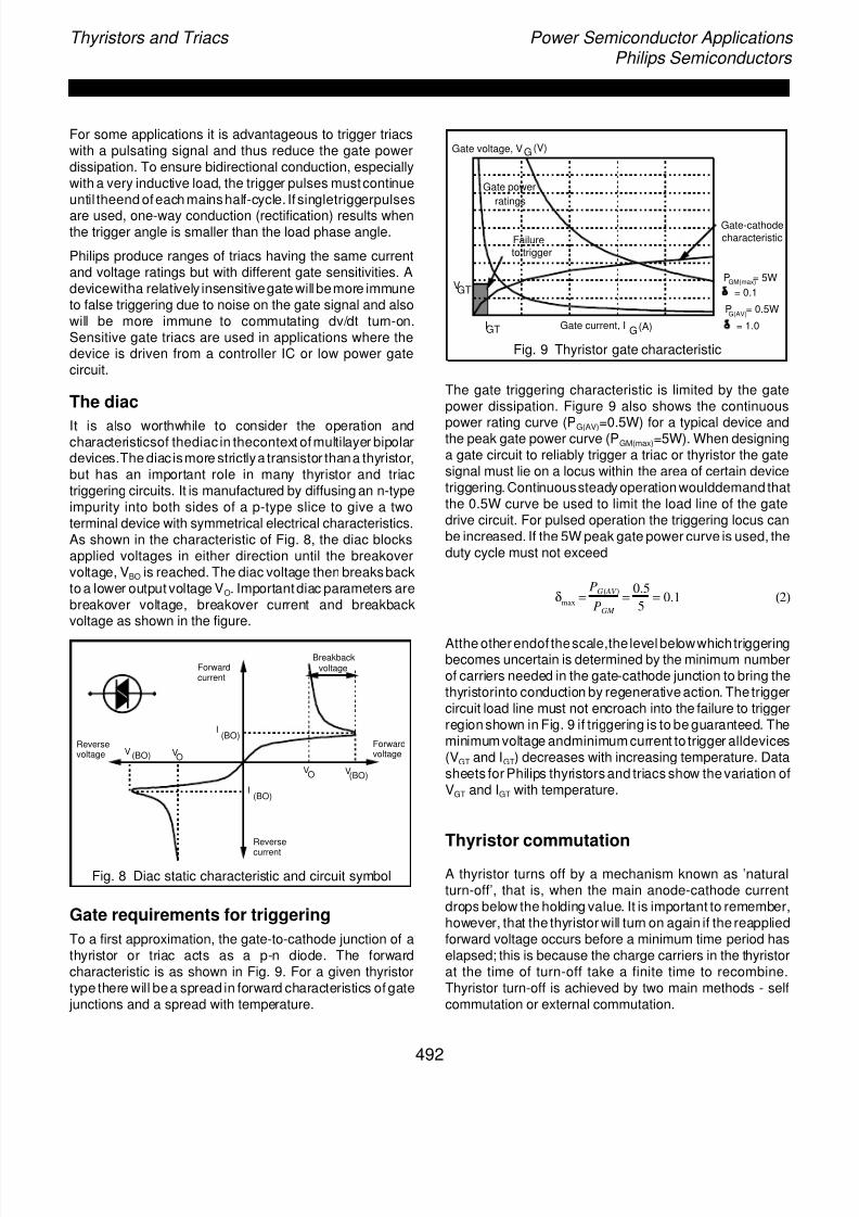
Gate requirements for triggering
To a first approximation, the gate-to-cathode junction of athyristor or triac acts as a p-n diode. The forwardcharacteristic is as shown in Fig. 9. For a given thyristortype there will bea spread in forward characteristics of gate
junctions and a spread with temperature.
Fig. 9 Thyristor gate characteristic
The gate triggering characteristic is limited by the gatepower dissipation. Figure 9 also shows the continuous
power rating curve (PG(AV)=0.5W) for a typical device andthe peak gate power curve (PGM(max)=5W). When designinga gate circuit to reliably trigger a triac or thyristor the gatesignal must lie on a locus within the area of certain devicetriggering. Continuoussteady operation woulddemand thatthe 0.5W curve be used to limit the load line of the gatedrive circuit. For pulsed operation the triggering locus canbe increased. If the 5W peak gate power curve is used, theduty cycle must not exceed
Atthe otherendof thescale,the level belowwhichtriggeringbecomes uncertain is determined by the minimum numberof carriers needed in the gate-cathode junction to bring thethyristorinto conduction by regenerative action. The triggercircuit load line must not encroach into the failure to triggerregion shown in Fig. 9 if triggering is to be guaranteed. Theminimum voltage andminimum current to trigger alldevices(VGT and IGT) decreases with increasing temperature. Datasheets for Philips thyristors and triacs show the variation ofVGT and IGT with temperature.
Thyristor commutation
A thyristor turns off by a mechanism known as ’naturalturn-off’, that is, when the main anode-cathode currentdrops below the holding value. It is important to remember,however, that the thyristor will turn on again if the reappliedforward voltage occurs before a minimum time period haselapsed; this is because the charge carriers in the thyristorat the time of turn-off take a finite time to recombine.Thyristor turn-off is achieved by two main methods - selfcommutation or external commutation.
Gate voltage, V G (V)
Gate current, IG(A)
P = 5W
= 0.1
= 1.0
VGT
IGT
Failureto trigger
GM(max)
P = 0.5WG(AV)
Gate power
ratings
Gate-cathodecharacteristic
δmax
= PG( AV )
PGM
= 0.5
5 = 0.1 (2)
Reverse
current
Forwardcurrent
Reversevoltage
Forwardvoltage
V(BO)
(BO)V
I(BO)
I(BO)
VO
VO
Breakbackvoltage
492
7/25/2019 Thyristors and Triacs
http://slidepdf.com/reader/full/thyristors-and-triacs 9/84
Thyristors and Triacs Power Semiconductor Applications Philips Semiconductors
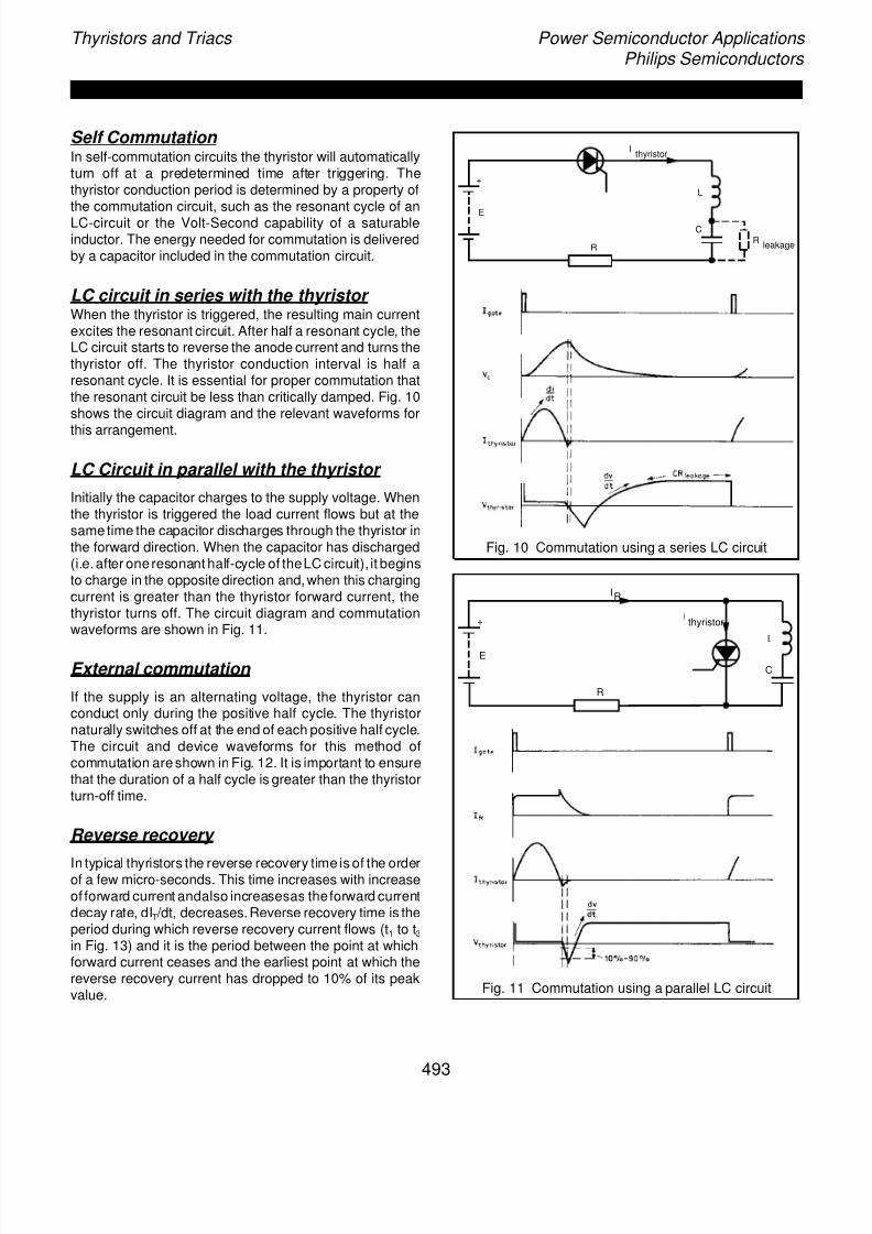
Self Commutation In self-commutation circuits the thyristor will automaticallyturn off at a predetermined time after triggering. Thethyristor conduction period is determined by a property ofthe commutation circuit, such as the resonant cycle of anLC-circuit or the Volt-Second capability of a saturableinductor. The energy needed for commutation is deliveredby a capacitor included in the commutation circuit.
LC circuit in series with the thyristor When the thyristor is triggered, the resulting main currentexcites the resonant circuit. After half a resonant cycle, theLC circuit starts to reverse the anode current and turns thethyristor off. The thyristor conduction interval is half aresonant cycle. It is essential for proper commutation thatthe resonant circuit be less than critically damped. Fig. 10shows the circuit diagram and the relevant waveforms for
this arrangement.
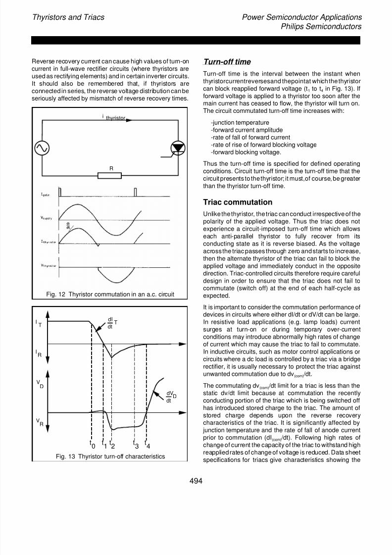
LC Circuit in parallel with the thyristor
Initially the capacitor charges to the supply voltage. Whenthe thyristor is triggered the load current flows but at thesame time the capacitor discharges through the thyristor inthe forward direction. When the capacitor has discharged(i.e.after oneresonant half-cycle of theLC circuit), it beginsto charge in the opposite direction and, when this chargingcurrent is greater than the thyristor forward current, thethyristor turns off. The circuit diagram and commutationwaveforms are shown in Fig. 11.
External commutation
If the supply is an alternating voltage, the thyristor canconduct only during the positive half cycle. The thyristornaturally switches off at the end of each positive half cycle.The circuit and device waveforms for this method ofcommutation are shown in Fig. 12. It is important to ensurethat the duration of a half cycle is greater than the thyristorturn-off time.
Reverse recovery
In typical thyristors the reverse recovery time is of the orderof a few micro-seconds. This time increases with increaseof forward current andalso increasesas theforward currentdecay rate, dIT /dt, decreases.Reverse recovery time is theperiod during which reverse recovery current flows (t1 to t3in Fig. 13) and it is the period between the point at whichforward current ceases and the earliest point at which thereverse recovery current has dropped to 10% of its peakvalue.
Fig. 10 Commutation using a series LC circuit
Fig. 11 Commutation using a parallel LC circuit
RR
leakage
L
CE
+
Ithyristor
R
L
C
E
IR
+ Ithyristor
493
7/25/2019 Thyristors and Triacs
http://slidepdf.com/reader/full/thyristors-and-triacs 10/84
Thyristors and Triacs Power Semiconductor Applications Philips Semiconductors
Reverse recovery current can cause high values of turn-oncurrent in full-wave rectifier circuits (where thyristors areused as rectifying elements) and in certain inverter circuits.It should also be remembered that, if thyristors areconnected in series, the reverse voltage distribution canbe
seriously affected by mismatch of reverse recovery times.
Fig. 12 Thyristor commutation in an a.c. circuit
Fig. 13 Thyristor turn-off characteristics
Turn-off time
Turn-off time is the interval between the instant whenthyristorcurrentreversesand thepointat whichthethyristorcan block reapplied forward voltage (t1 to t4 in Fig. 13). If
forward voltage is applied to a thyristor too soon after themain current has ceased to flow, the thyristor will turn on.The circuit commutated turn-off time increases with:
-junction temperature-forward current amplitude-rate of fall of forward current-rate of rise of forward blocking voltage-forward blocking voltage.
Thus the turn-off time is specified for defined operatingconditions. Circuit turn-off time is the turn-off time that thecircuit presents to thethyristor; it must,of course, be greaterthan the thyristor turn-off time.
Triac commutation
Unlike thethyristor, thetriac canconduct irrespectiveof thepolarity of the applied voltage. Thus the triac does notexperience a circuit-imposed turn-off time which allowseach anti-parallel thyristor to fully recover from itsconducting state as it is reverse biased. As the voltageacrossthe triac passes through zero andstarts to increase,then the alternate thyristor of the triac can fail to block theapplied voltage and immediately conduct in the oppositedirection. Triac-controlled circuits therefore require carefuldesign in order to ensure that the triac does not fail tocommutate (switch off) at the end of each half-cycle asexpected.
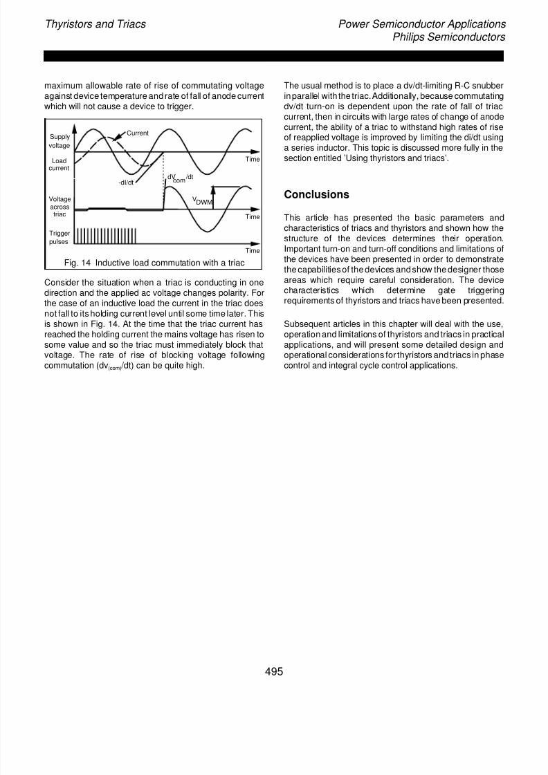
It is important to consider the commutation performance ofdevices in circuits where either dI/dt or dV/dt can be large.In resistive load applications (e.g. lamp loads) currentsurges at turn-on or during temporary over-currentconditions may introduce abnormally high rates of changeof current which may cause the triac to fail to commutate.In inductive circuits, such as motor control applications orcircuits where a dc load is controlled by a triac via a bridgerectifier, it is usually necessary to protect the triac againstunwanted commutation due to dv(com) /dt.
The commutating dv(com)
/dt limit for a triac is less than thestatic dv/dt limit because at commutation the recentlyconducting portion of the triac which is being switched offhas introduced stored charge to the triac. The amount ofstored charge depends upon the reverse recoverycharacteristics of the triac. It is significantly affected by
junction temperature and the rate of fall of anode currentprior to commutation (dI(com) /dt). Following high rates ofchange of current the capacity of the triac to withstand highreappliedrates of change of voltage is reduced. Data sheetspecifications for triacs give characteristics showing the
R
i thyristor
IT
IR
V
D
VR
dIT
dt
dVD
dt
t0
t1 t2
t3
t4
494
7/25/2019 Thyristors and Triacs
http://slidepdf.com/reader/full/thyristors-and-triacs 11/84
Thyristors and Triacs Power Semiconductor Applications Philips Semiconductors
maximum allowable rate of rise of commutating voltageagainst device temperature andrate of fall of anode currentwhich will not cause a device to trigger.
Fig. 14 Inductive load commutation with a triac
Consider the situation when a triac is conducting in onedirection and the applied ac voltage changes polarity. Forthe case of an inductive load the current in the triac doesnot fall to its holding current level until some time later. Thisis shown in Fig. 14. At the time that the triac current hasreached the holding current the mains voltage has risen tosome value and so the triac must immediately block thatvoltage. The rate of rise of blocking voltage followingcommutation (dv(com) /dt) can be quite high.
The usual method is to place a dv/dt-limiting R-C snubberinparallel with the triac.Additionally, because commutatingdv/dt turn-on is dependent upon the rate of fall of triaccurrent, then in circuits with large rates of change of anodecurrent, the ability of a triac to withstand high rates of rise
of reapplied voltage is improved by limiting the di/dt usinga series inductor. This topic is discussed more fully in thesection entitled ’Using thyristors and triacs’.
Conclusions
This article has presented the basic parameters andcharacteristics of triacs and thyristors and shown how thestructure of the devices determines their operation.Important turn-on and turn-off conditions and limitations ofthe devices have been presented in order to demonstrate
the capabilitiesof the devices andshow the designer thoseareas which require careful consideration. The devicecharacteristics which determine gate triggeringrequirements of thyristors and triacs have been presented.
Subsequent articles in this chapter will deal with the use,operation and limitations of thyristors and triacs in practicalapplications, and will present some detailed design andoperational considerations for thyristors and triacs in phasecontrol and integral cycle control applications.
VDWM
-dI/dtdV
com /dt
Time
Time
Time
Supplyvoltage
Loadcurrent
Voltageacrosstriac
Trigger
pulses
Current
495

7/25/2019 Thyristors and Triacs
http://slidepdf.com/reader/full/thyristors-and-triacs 12/84

7/25/2019 Thyristors and Triacs
http://slidepdf.com/reader/full/thyristors-and-triacs 13/84
Thyristors and Triacs Power Semiconductor Applications Philips Semiconductors
6.1.2 Using Thyristors and Triacs
This chapter is concerned with the uses, operation and
protection of thyristors andtriacs. Twotypes of circuit coverthe vast majority of applications for thyristors and triacs:static switching circuits and phase control circuits. Thecharacteristics anduses of these two types of circuit will bediscussed. Various gate drive circuits and protectioncircuits for thyristor and triacs are also presented. The useofthesecircuitswill enabledesigners tooperate thedevicesreliably and within their specified limits.
Thyristor and triac control techniques
There are two main techniques of controlling thyristors andtriacs - on-off triggering (or static switching) and phasecontrol. In on-off triggering, the power switch is allowed to
conduct for a certain number of half-cycles and then it iskept off for a number of half-cycles. Thus, by varying theratio of "on-time" to "off-time", the average power suppliedto the load can be controlled. The switching device eithercompletely activates or deactivates the load circuit. Inphase control circuits, the thyristor or triac is triggered intoconduction at some point after the start of each half-cycle.Control is achieved on a cycle-by-cycle basis by variationof the point in the cycle at which the thyristor is triggered.
Static switching applications
Thyristors and triacs are the ideal power switching devicesfor many high power circuits such as heaters, enabling the
load to be controlled by a low power signal, in place of arelay or other electro-mechanical switch.
Ina highpower circuit where the power switch may connector disconnect the load at any point of the mains cycle thenlarge amounts of RFI (radio frequency interference) arelikely to occur at the instants of switching. The largevariations in load may also cause disruptions to the supplyvoltage. The RFI and voltage variation produced by highpower switching in a.c. mains circuits is unacceptable inmany environments and is controlled by statutory limits.The limits depend upon the type of environment (industrialor domestic) and the rating of the load being switched.
RFI occurs at any time when there is a step change incurrent caused by the closing of a switch (mechanical orsemiconductor). The energy levels of this interference canbequitehigh in circuitssuch as heating elements.However,if the switch is closed at the moment the supply voltagepasses through zero there is no step rise in current andthus no radio frequency interference. Similarly, at turn-off,a large amount of high frequency interference can becaused by di/dt imposed voltage transients in inductivecircuits.
Circuit-generated RFIcanbe almost completely eliminated
by ensuring that the turn-on switching instants correspondto the zero-crossing points of the a.c. mains supply. Thistechnique is known as synchronous (or zero voltage)switching control as opposed to the technique of allowingthe switching points to occur at any time during the a.c.cycle, which is referred to as asynchronous control.
In a.c. circuits using thyristors and triacs the devicesnaturally switch off when the current falls below the deviceholding current. Thus turn-off RFI does not occur.
Asynchronous control
In asynchronous control the thyristor or triac may betriggeredat a point in the mains voltage other than the zerovoltage crossover point. Asynchronous control circuits areusually relatively cheap but liable to produce RFI.
Synchronous control
In synchronous control systems the switching instants aresynchronised with zero crossings of the supply voltage.They also have the advantage that, as the thyristorsconduct over complete half cycles, the power factor is verygood.This methodofpowercontrol ismostlyused tocontrol
temperature.Therepetition period, T, is adjusted to suit thecontrolled process (within statutory limits). Temperaturerippleis eliminated when therepetitionperiodis made muchsmaller than the thermal time constant of the system.
Figure 1 shows the principle of time-proportional control.RFIand turn-on di/dtarereduced,andthe best power factor(sinusoidal load current) is obtained by triggeringsynchronously. The average power delivered to a resistiveload, RL, is proportional to ton /T (i.e. linear control) and isgiven by equation 1.
where: T is the controller repetition periodton is controller ’on’ timeV(RMS) is the rms a.c. input voltage.
Elsewhere in this handbook theoperationof a controller i.c.(the TDA1023) is described. This device is specificallydesigned to implement time-proportional control of heatersusing Philips triacs.
Pout = V ( RMS )
2
R L
.t on
T (1)
497
7/25/2019 Thyristors and Triacs
http://slidepdf.com/reader/full/thyristors-and-triacs 14/84
Thyristors and Triacs Power Semiconductor Applications Philips Semiconductors
Fig. 1 Synchronous time-proportional control
Phase control
Phase control circuits are used for low power applications
such as lamp control or universal motor speed control,where RFI emissions can be filtered relatively easily. Thepower delivered to the load is controlled by the timing ofthe thyristor (or triac) turn-on point.
The two most common phase controller configurations are’half wave control’, where the controlling device is a singlethyristorand’fullwave control’,where thecontrollingdeviceis a triac or a pair of anti-parallel thyristors. These twocontrol strategies are considered in more detail below:
Resistive loads
The operation of a phase controller with a resistive load is
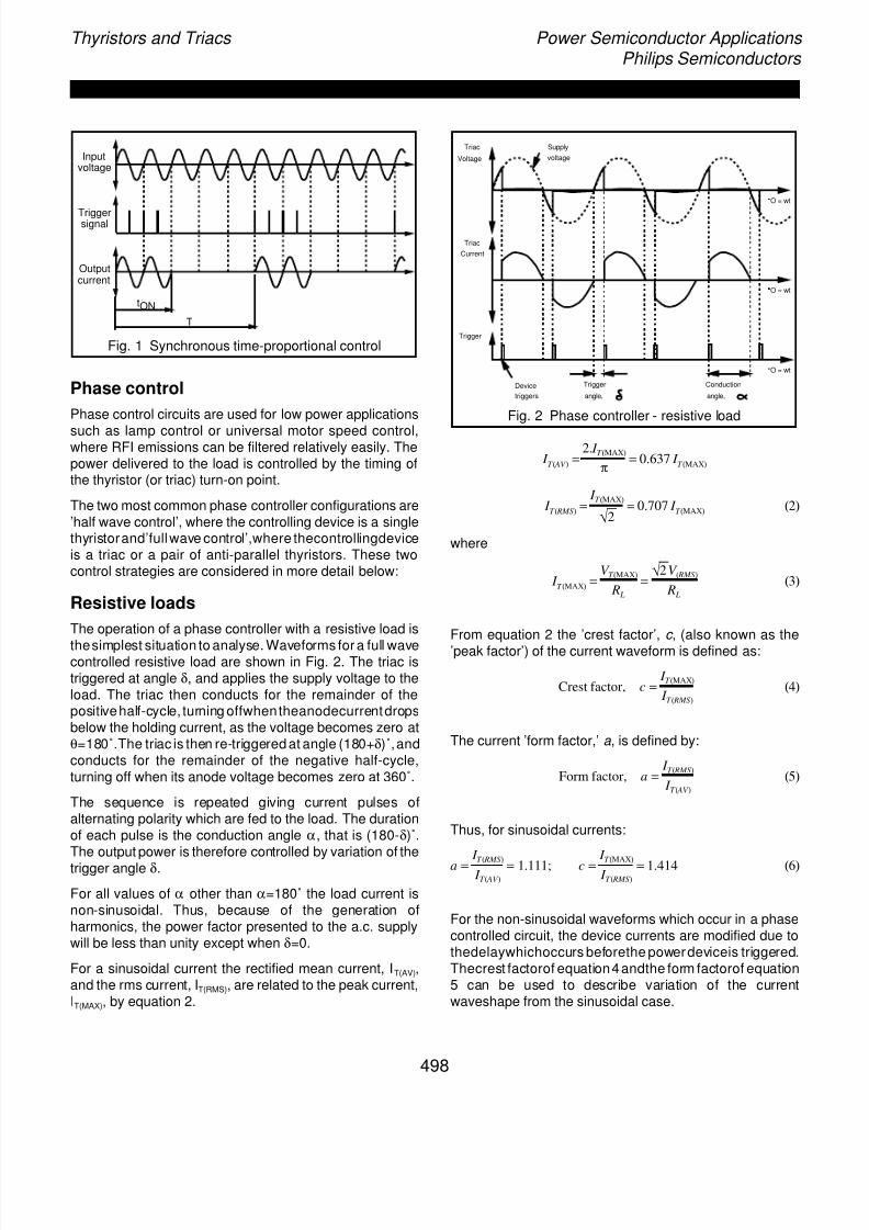
thesimplest situation to analyse. Waveforms for a full wavecontrolled resistive load are shown in Fig. 2. The triac istriggered at angle δ, and applies the supply voltage to theload. The triac then conducts for the remainder of thepositivehalf-cycle, turning offwhentheanodecurrentdropsbelow the holding current, as the voltage becomes zero atθ=180˚.The triac is then re-triggered at angle (180+δ)˚,andconducts for the remainder of the negative half-cycle,turning off when its anode voltage becomes zero at 360˚.
The sequence is repeated giving current pulses ofalternating polarity which are fed to the load. The durationof each pulse is the conduction angle α, that is (180-δ)˚.The output power is therefore controlled by variation of thetrigger angle δ.
For all values of α other than α=180˚ the load current isnon-sinusoidal. Thus, because of the generation ofharmonics, the power factor presented to the a.c. supplywill be less than unity except when δ=0.
For a sinusoidal current the rectified mean current, IT(AV),and the rms current, IT(RMS), are related to the peak current,IT(MAX), by equation 2.
Fig. 2 Phase controller - resistive load
where
From equation 2 the ’crest factor’, c , (also known as the
’peak factor’) of the current waveform is defined as:
The current ’form factor,’ a , is defined by:
Thus, for sinusoidal currents:
For the non-sinusoidal waveforms which occur in a phasecontrolled circuit, the device currents are modified due tothedelaywhichoccurs beforethe powerdeviceis triggered.Thecrest factorof equation4andthe form factorof equation5 can be used to describe variation of the currentwaveshape from the sinusoidal case.
tON
T
Inputvoltage
Triggersignal
Outputcurrent
Trigger
Conduction
angle,
Voltage
Current
Supply
voltage
Triac
Triac
Device
triggers
Trigger
angle,
O = wt
O = wt
O = wt
I T ( AV ) =
2. I T (MAX)
π = 0.637 I
T (MAX)
I T ( RMS ) =
I T (MAX)
√ 2= 0.707 I
T (MAX) (2)
I T (MAX) =
V T (MAX)
R L
= √ 2V ( RMS )
R L
(3)
Crest factor, c = I T (MAX)
I T ( RMS )(4)
Form factor, a = I T ( RMS )
I T ( AV )(5)
a = I
T ( RMS ) I T ( AV )
= 1.111; c = I
T (MAX) I T ( RMS )
= 1.414 (6)
498

7/25/2019 Thyristors and Triacs
http://slidepdf.com/reader/full/thyristors-and-triacs 15/84
Thyristors and Triacs Power Semiconductor Applications Philips Semiconductors
Half wave controller
Figure 3a) shows the simplest type of thyristor half-wavephase controller for a resistive load. The load currentwaveform is given in Fig. 3b). Thevariationof average load
current, IT(AV), rms load current, IT(RMS) and load power overthe full period of the a.c mains, with trigger angle are givenin equation 7.
N.B. When using equation 7 all values of α must be inradians. For each case the maximum value occurs whenα=180˚ (α=π radians).
At α=180˚ the crest factor and form factor for a half wavecontroller are given by:
Full wave controller
Figure 4 shows the circuit and load current waveforms fora full-wave controller using two antiparallel thyristors, or atriac, as the controlling device. The variation of rectifiedmean current, IT(AV), rms current, IT(RMS), and load power withtrigger angle are given by equation 9.
N.B. When using equation 9 all value of α must be inradians. For each case the maximum value occurs whenα=180˚ (α=π radians).
Fig. 3 Half wave control
Fig. 4 Full wave control
The variation of normalised average current, IT(AV) /IT(AV)max,rms current IT(RMS) /IT(RMS)max, and power, P(out) /P(out)max, for
equations 7 and 9 are plotted in Fig. 5.
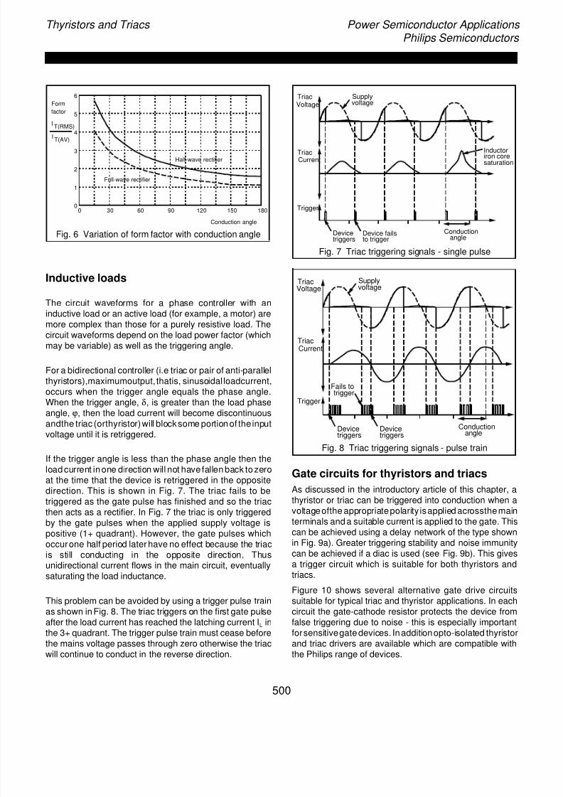
Figure 6 shows the variation of current form factor withconduction angle for the half wave controller and the fullwave controller of Figs. 3 and 4.
Fig. 5 Current and power control using conductionangle
a) b)
Trigger
Voltage
Current
Supplyvoltage
Thyristor
Thyristor
IT(MAX)
I T ( AV ) = I T ( AV )max.
(1− cosα)2
I T ( RMS ) = I T ( RMS )max.
α − 1
2sin2α
π
1
2
P(out ) = P(out )max.
α − 1
2sin2απ
I T ( AV )max =
I T (MAX)
π
I T ( RMS )max =
I T (MAX)
2
P(out )max =
I T (MAX)2
R L
4 (7
)
a) b)
Trigger
Voltage
Current
Supplyvoltage
Triac
Triac
IT(MAX)
IT(MAX)
a = I T ( RMS )
I T ( AV )= 1.571; c =
I T (MAX)
I T ( RMS )= 2.0 (8)
IT(AV)
IT(AV)max
IT(RMS)
IT(RMS)max
P(OUT)
P(OUT)max
A m p l i t u d e
Conduction angle
0 30 60 90 120 150 1800
0.2
0.4
0.6
0.8
1
I T ( AV ) = I T ( AV )max.
(1− cosα)2
I T ( RMS ) = I T ( RMS )max. α −
1
2
sin2
απ
1
2
P(out ) = P(out )max.
α − 1
2sin2α
π
I T ( AV )max =
2 I T (MAX)
π
I T
( RMS
)max
= I T (MAX)
√ 2
P(out )max = I T (MAX)2
R L
2 (9)
499
7/25/2019 Thyristors and Triacs
http://slidepdf.com/reader/full/thyristors-and-triacs 16/84
Thyristors and Triacs Power Semiconductor Applications Philips Semiconductors
Fig. 6 Variation of form factor with conduction angle
Inductive loads
The circuit waveforms for a phase controller with aninductive load or an active load (for example, a motor) aremore complex than those for a purely resistive load. Thecircuit waveforms depend on the load power factor (whichmay be variable) as well as the triggering angle.
For a bidirectional controller (i.e triac or pair of anti-parallelthyristors),maximumoutput, thatis, sinusoidal loadcurrent,occurs when the trigger angle equals the phase angle.When the trigger angle, δ, is greater than the load phaseangle, ϕ, then the load current will become discontinuousandthe triac (orthyristor)will blocksome portion of the inputvoltage until it is retriggered.
If the trigger angle is less than the phase angle then theload current inone direction will not have fallen back to zeroat the time that the device is retriggered in the oppositedirection. This is shown in Fig. 7. The triac fails to betriggered as the gate pulse has finished and so the triacthen acts as a rectifier. In Fig. 7 the triac is only triggeredby the gate pulses when the applied supply voltage ispositive (1+ quadrant). However, the gate pulses whichoccurone half period later have no effect because the triac
is still conducting in the opposite direction. Thusunidirectional current flows in the main circuit, eventuallysaturating the load inductance.
This problem can be avoided by using a trigger pulse trainas shown in Fig. 8. The triac triggers on the first gate pulseafter the load current has reached the latching current IL inthe 3+ quadrant. The trigger pulse train must cease beforethe mains voltage passes through zero otherwise the triacwill continue to conduct in the reverse direction.
Fig. 7 Triac triggering signals - single pulse
Fig. 8 Triac triggering signals - pulse train
Gate circuits for thyristors and triacs
As discussed in the introductory article of this chapter, athyristor or triac can be triggered into conduction when avoltageofthe appropriatepolarity isapplied acrossthemainterminals and a suitable current is applied to the gate. Thiscan be achieved using a delay network of the type shownin Fig. 9a). Greater triggering stability and noise immunitycan be achieved if a diac is used (see Fig. 9b). This givesa trigger circuit which is suitable for both thyristors andtriacs.
Figure 10 shows several alternative gate drive circuitssuitable for typical triac and thyristor applications. In eachcircuit the gate-cathode resistor protects the device fromfalse triggering due to noise - this is especially importantforsensitivegate devices. Inadditionopto-isolated thyristorand triac drivers are available which are compatible withthe Philips range of devices.
Form
factor
IT(RMS)
I T(AV)
Conduction angle
0 30 60 90 120 150 1800
1
2
3
4
5
6
Half-wave rectifier
Full-wave rectifier
Trigger
Device failsto trigger
Conductionangle
Voltage
Current
Supplyvoltage
Triac
Triac Inductoriron coresaturation
Devicetriggers
Trigger
Conductionangle
Voltage
Current
Supplyvoltage
Triac
Triac
Devicetriggers
Devicetriggers
Fails totrigger
500
7/25/2019 Thyristors and Triacs
http://slidepdf.com/reader/full/thyristors-and-triacs 17/84
Thyristors and Triacs Power Semiconductor Applications Philips Semiconductors
Fig. 10 Alternative triac triggering circuits
1k0
220R
BT145
Load
1k0BT145
Load
180R
10k
12V
BC337
1k0
Load
10k
12V
1k0
Load
10k
12V
BC337
4k7100nF
BT145
BT145BAW62
2:1
a)
b)
Fig. 9 Basic triac triggering circuits
In some applications it may be necessary to cascade asensitive gate device with a larger power device to give asensitive gate circuit with a high power handling capability.A typical solution which involves triggering the smallerdevice (BT169) from a logic-level controller to turn on thelarger device (BT151) is shown in Fig. 11.
Figure 12 shows an isolated triac triggering circuit suitablefor zero voltage switching applications. This type of circuitis also known as a solid state relay (SSR). The function of
the Q1/R2/R3 stage is that the BC547 is on at all instantsin time when the applied voltage waveform is high and thusholds the BT169 off. If the BT169 is off then no gate signalis applied to the triac and the load is switched off.
Fig. 11 Master-slave thyristor triggering circuit
Fig. 12 Opto-isolated triac triggering circuit
R
E
IR
+
R
E
IR
+ BT151BT169
R
IR
+
-
R1R3
R2 R4
BC547
BT169
100R
1K0
BT138100R
100nF
Q1
501
7/25/2019 Thyristors and Triacs
http://slidepdf.com/reader/full/thyristors-and-triacs 18/84
Thyristors and Triacs Power Semiconductor Applications Philips Semiconductors
If the input signal is switched high then the photo-transistorturns on. If this occurs when the mains voltage is high thenQ1 remains on. When the line voltage passes through itsnext zero crossing in either direction the photo transistorensures that Q1 stays off long enough for the BT169 to
trigger. This then turns the triac on. Once the thyristor turnson, the drive circuit is deprived of its power due to the lowervoltage drop of the BT169. The triac is retriggered everyhalf cycle.
Voltage transient protection
Therearethree major sources of transientwhichmayaffectthyristor and triac circuits:
-the mains supply (e.g. lightning)-other mains and load switches (opening and closing)-the rectifying and load circuit (commutation)
In order to ensure reliable circuit operation these transientsmust be suppressed by additional components, removedat source or allowed for in component ratings.
Three types of circuit are commonly employed to suppressvoltage transients - a snubber network across the device,a choke between the power device and external circuit oran overvoltage protection such as a varistor.
Series line chokes
A series choke may be used to limit peak fault currents toassist in the fuse protection of thyristors and triacs. If thechoke is used in conjunction with fuse protection, it mustretain its inductance to very large values of current, and so
for this reason it is usually an air-cored component.Alternatively,if thechokeis only requiredto reducethe dv/dtacross non-conducting devices then the inductance needsonly to be maintained up toquite lowcurrents. Ferrite-coredchokes may be adequate provided that the windings arecapable of carrying the full-load current. Usually only a fewmicrohenries of inductance are required to limit the circuitdi/dt to an acceptable level. This protects the devices fromturning on too quickly and avoids potential devicedegradation.
For instance, a 220V a.c. supply with 20µH sourceinductance gives a maximum di/dt of (220√2)/20=16A/ µs.Chokes used to soften commutation should preferably besaturable so as to maintain regulation and avoiddeterioration of the power factor. As their impedancereduces at high current, they have very little effect on theinrush current.
The addition of di/dt limiting chokes is especially importantin triac circuits where the load is controlled via a bridgerectifier. At the voltage zero-crossing points the conductiontransfers between diodes in the bridge network, and therate of fall of triac current is limited only by the strayinductance in the a.c. circuit. The large value ofcommutating di/dt may cause the triac to retrigger due to
commutating dv(com) /dt. A small choke in the a.c circuit willlimit the di(com) /dt to an acceptable level. An alternativetopology which avoids triac commutation problems is tocontrol the load on the d.c. side.
Snubber networks
Snubber networks ensure that the device is not exposed toexcessive rates of change of voltage during transientconditions. This is particularly important when consideringthe commutation behaviour of triacs, which has beendiscussed elsewhere.
Fig. 13 Triac protection
Thefollowing equationscanbe used to calculatethe valuesof the snubber components required to keep the reapplieddv/dt for a triac within the dv(com) /dt rating for that device.The parameters which affect the choice of snubbercomponentsare the value of load inductance, frequency ofthe a.c. supply and rms load current. The value of thesnubber resistor needs to be large enough to damp thecircuitandavoidvoltageovershoots. Thesnubbercapacitorshould be rated for the full a.c. voltage of the system. Thesnubber resistor needs to be rated at 0.5W.
For circuits where the load power factor, cosϕ, ≥ 0.7 thesnubber values are given approximately by:
where: L is the load inductancef is the supply frequencyIT(RMS) is the rms device currentdv(com) /dt is the device commutating dv/dt rating.
The presence of a snubber across the device can improvethe turn-on performance of the triac by using the snubbercapacitor discharge current in addition to the load currentto ensure that the triac latches at turn-on. The value of thesnubber resistor must be large enough to limit the peakcapacitor discharge current through the triac to within theturn-on di/dt limit of the device.
Load
SnubberVaristor
Choke
C ≥ 25 L
fI T ( RMS )
dV (com)/dt
2
R = √ 3 L
C (9)
502
7/25/2019 Thyristors and Triacs
http://slidepdf.com/reader/full/thyristors-and-triacs 19/84
Thyristors and Triacs Power Semiconductor Applications Philips Semiconductors
Varistor
The use of a metal oxide varistor (MOV), as shown inFig. 13, protects the device from transient overvoltageswhich may occur due to mains disturbances.
Overcurrent protection
Like all other semiconductor devices, triacshave an infinitelife if they are used within their ratings. However, theyrapidly overheat when passing excessive current becausethe thermal capacitance of their junction is small.Overcurrent protective devices (circuit breakers, fuses)must, therefore, be fast-acting.
Inrush condition
Motors, incandescent lamp or transformer loads give riseto an inrush condition. Lamp and motor inrush currents areavoided by starting the control at a large trigger angle.
Transformer inrush currents are avoided by adjusting theinitial trigger angle toa valueroughlyequalto theloadphaseangle. No damage occurs when the amount of inrushcurrent is below the inrush current rating curve quoted inthe device data sheet (see the chapter ’Understandingthyristor and triac data’).
Short-circuit condition
Fuses for protecting triacs should be fast acting, and theamount of fuse I2t to clear the circuit must be less than theI2t rating of the triac. Because the fuses open the circuit
rapidly, they have a current limiting action in the event of ashort-circuit. High voltage fuses exhibit low clearing I2t butthe fuse arc voltage may be dangerous unless triacs witha sufficiently high voltage rating are used.
Conclusions
This paper has outlined the most common uses andapplicationsof thyristorand triac circuits.The type of circuitused depends upon the degree of control required and thenature of the load. Several types of gate circuit and deviceprotection circuit have been presented. The amount of
device protection required will depend upon the conditionsimposed on the device by the application circuit. Theprotection circuits presented here will be suitable for themajority of applications giving a cheap, efficient overalldesign which uses the device to its full capability withcomplete protection and confidence.
503

7/25/2019 Thyristors and Triacs
http://slidepdf.com/reader/full/thyristors-and-triacs 20/84
7/25/2019 Thyristors and Triacs
http://slidepdf.com/reader/full/thyristors-and-triacs 21/84
Thyristors and Triacs Power Semiconductor Applications Philips Semiconductors
6.1.3 The Peak Current Handling Capability of Thyristors
The ability of a thyristor to withstand peak currents many
times the size of its average rating is well known. However,there is little informationabout thefactors affectingthe peakcurrent capability. This section will investigate the effect ofpulse duration on the peak current capability of thyristors.
Data sheets for thyristors always quote a figure for themaximum surge current that the device can survive. Thisfigureassumesa halfsinepulse witha width of either10 msor 8.3 ms, which are the conditions applicable for 50/60 Hzmains operation. This limit is not absolute; narrow pulseswith much higher peaks can be handled without damagebut little information is available to enable the designer todetermine how high this current is. This section will discusssome of the factors affecting a thyristor’s peak currentcapability andreview the existing prediction methods. It willgo on to present the results of an evaluation of the peakcurrent handling capabilities for pulses as narrow as 10 µsfor the BT151, BT152 and BT145 thyristors. It will alsopropose a method for estimating a thyristor’s peak currentcapability fora half sine pulsewith a durationbetween10 µsand 10 ms from its quoted surge rating.
Energy Handling
Inaddition to themaximum surgecurrent, data sheetsoftenquote a figure called "I2t for fusing". This number is used toselectappopriate fuses fordevice protection. I2t represents
the energy that can be passed by the device withoutdamage. In fact it is not the passage of the energy whichcausesdamage,butthe heating of thecrystal by the energyabsorbed by the device which causes damage.
If the period over which the energy is delivered is long, theabsorbed energy has time to spread to all areas of thedevice capable of storing it - like the edges of the crystal,the plastic encapsulation, the mounting tab and for verylong times the heatsink - therefore the temperature rise inthe crystal is moderated. If, however, the delivery period isshort - say a single half sine pulse of current with a durationof <10 ms - the areas to which the energy can spread for
the actualduration of the pulse are limited. This means thatthe crystal keeps all the energy giving a much biggertemperature rise. Forvery short pulses (<0.1 ms)and largecrystal, the problem is even worse because not all of theactivearea of a thyristorcrystal is turned on simultaneously- conduction tends to spread out from the gate area - sothe current pulse passes through only part of the crystalresulting in a higher level of dissipation and an even morerestricted area for absorbing it.
Expected Results
I2t is normally quoted at 10 ms, assuming that the surge isa half sine pulse,and is derived from thesurge current from:
This calculates the RMS current by dividing by
Under the simplest of analyses I2t would be assumed to beconstant so a device’s peak current capability could becalculated from:
where Ipk is the peak of a half sine current pulse with aduration of tp. However, experience and experiments haveshown that such an approach is inaccurate. To overcomethis, other ’rules’ have been derived.
One of these ’rules’ suggests that it is not I2t which isconstant but I3t or I4t. Another suggestion is that the’constancy’ continuously changes from I2t to I4t as thepulsesbecomeshorter. All these rules areexpressedin thegeneral equation:
where isN iseitherconstant or a function of the pulse width,for example:
The graph shown in Fig. 1 shows what several of these’rules’ predict would happen to the peak current capabilityif they were true. Unfortunately little or no real informationcurrently exists to indicate the validity of these rules. Testshave been performed on three groups of devices - BT151,BT152 and BT145 - to gather the data which would,
hopefully, decide which was correct.
Test Circuit
The technique chosen to measure the peak currentcapability of the devices was the stepped surge method. Inthis test, thedeviceis subjectedto a seriesof current pulsesof increasing magnitude until it receives a surge whichcauses measurable degradation.
I 2t =
I TSM
√ 2
2
0.01
√ 2 I TSM
I pk =
I TSM
0.01
t p
1
2
I pk = I TSM
0.01
t p
1
N
N = log
1
t p
505
7/25/2019 Thyristors and Triacs
http://slidepdf.com/reader/full/thyristors-and-triacs 22/84
Thyristors and Triacs Power Semiconductor Applications Philips Semiconductors
Fig. 1 Predicted ITSM multiplying factors
Circuit Description
The circuits used to perform the required measurementswere of the form shown in Fig. 2. They produce half sinepulses of current from the resonant discharge of C via L.Triggering of the device under test (DUT) itself is used toinitiate the discharge. The gate signal used for all the testswas a 100 mA / 1 µs pulse fed from a pulse generator insingle-shot mode.
Themagnitudeof thecurrent pulse is adjusted by changing
the voltage to which C is initially charged by varying theoutput of the PSU. The pulse is monitored by viewing thevoltage across R3 on an digital storage oscilloscope. R1and D protect the power supply. R1 limits the current fromthe supply when DUT fails and during the recharging of C.D attempts to prevent any high voltage spikes being fedback into the PSU.
Fig. 2 Surge current test circuit
Pushbutton S1 and resistor R2 are a safety feature. R2keeps C discharged until S1 is pressed. The trigger pulseneeds a button on the pulse generator to be pressed whichmeans both hands are occupied and kept away from thetest circuit high voltages.
Choice of L & C
The width of the half sine pulse from an LC circuit is:
and the theoretical peak value of the current is:
These equations assume that the circuit has no seriesresistance to damp the resonant action which would resultin a longer but lower pulse. Minimising these effects wasconsidered to be important so care was taken during thebuilding of the circuits to keep the resistance to a minimum.To this end capacitors with low ESR were chosen, theinductorswere wound using heavy gauge wire and the loopC / L / DUT / R3 was kept as short as possible.
It was decided to test the devices at three different pulsewidths - 10 µs, 100 µs and 1 ms - so three sets of L and Cwere needed. The values were selected with the help of a’spreadsheet’ program running on an PC compatiblecomputer.Thevalues which were finally chosen are shownin Table 1. Also given in Table 1 are the theoretical peakcurrents that the L / C combination would produce for ainitial voltage on C of 600 V.
Test Procedure
Asmentionedearlier, thetest methodcalled foreachdeviceto be subjected to a series of current pulses of increasingamplitude. The resolution with which the current capability
is assessed is defined by the size of each increase incurrent. It was decided that steps of approximately 5%would give reasonable resolution.
Experimentation indicated that the clearest indication ofdevice damage was obtained by looking for changes in theoff-state breakdown voltage. So after each current pulsethe DUT was removed from the test circuit and checked ona curve tracer. This procedure did slow the testing but itwas felt that it would result in greater accuracy.
Pulse Width C (µF) L (µH) Ipeak (A)
10 µs 13.6 0.75 2564
100 µs 100 10 1885
1 ms 660 154 1244
Table 1. Inductor and Capacitor Values
It was also decided that, since this work was attempting todeterminethe current that a devicecouldsurvive - notwhichkilledit, thefigure actuallyquotedin theresults fora device’scurrent capability would be the value of the pulse prior tothe one which caused damage.
15
14
13
12
11
10
9
8
7
6
5
4
3
2
110us 100us 1ms 10ms
Width of Half Sine Pulse
I t = const.
I t = const.
I t = const.
I t = const.log(1/t)
2
3
4
P e a k C u r r e n t M u l t i p l y i n g F a c t o r
t pulse = π √ L C
I peak = V √ C
L
DC PSU
0-600V
DR1 L
CR2
DUT
R3
S1 Vak
Trigger
Ia
Pulse
506

7/25/2019 Thyristors and Triacs
http://slidepdf.com/reader/full/thyristors-and-triacs 23/84
Thyristors and Triacs Power Semiconductor Applications Philips Semiconductors
Fig. 3 Peak current capability measurements
Test ResultsFigure 3 is a graph showing the measured currentcapabilitiesof all of the testeddevices. Table2 summarisesthe measurements bygiving the mean of the results for thethree device types at each of the pulse widths. Table 3expresses the mean values as factors of the device ITSM
rating. This table also gives the factors that the various’rules’ would have predicted for the various pulse widths.
Mean Peak Current Capability (Amps)
Pulse Width BT151 BT152 BT145
10 µs 912 1092 1333100 µs 595 1021 1328
1 ms 264 490 697
Table 2. Measured Current Capability
Measured Predicted FactorFactor (by Int rule)
Pulse BT BT BT n=2 n=3 n=4 n=Width 151 152 145 log(1/t)
10 µs 9.1 5.5 4.4 31.6 10.0 5.6 4.0
100 µs 6.0 5.1 4.4 10.0 4.6 3.2 3.2
1 ms 2.6 2.4 2.3 3.2 2.2 1.8 2.2
Table 3. Measured and Predicted ITSM MultiplicationFactors
Interpretation of Results
It had been hoped that the measurements would give clearindication of which of the ’rules’ would give the mostaccurate prediction of performance. However, aninspection of Table 3 clearly shows that there is no
correlation between any of the predicted factors and themeasured factors. In fact the variation in the factorsbetween the various device types would indicated that norule based on an Int function alone can give an accurateprediction. This implies that something else will have to be
taken into account.
FurtherstudyofFig. 3 reveals that thedifference in thepeakcurrent capability of the threedevice types is becoming lessas the pulses become shorter. This could be explained bya reduction in the active area of the larger crystals, makingthem appear to be smaller than they actually are. This isconsistent with theknownfact that notall areas ofa thyristorturn on simultaneously - the conduction region tends tospread out from the gate. If the pulse duration is less thanthe time it takes for all areas of the device to turn on, thenthe current flows through only part of the crystal, reducingthe effective size of the device. If the rate at which the
conduction area turns on is constant then the time takenfor a small device to be completely ON is shorter than fora large device. This would explain why the performanceincrease of the BT145 starts falling off before that of theBT151.
Proposed Prediction Method
The above interpretation leads one to believe that theoriginal energy handling rule, which says that I2t is aconstant, may still be correct but that the performance itpredicts will ’roll off’ if the pulse duration is less than somecritical value. The equation which was developed to havethe necessary characteristics is:
which simplifies to:-
where tcrit is proportional to - but not necessarily equal to -the time taken to turn on all the active area of the crystaland is calculated from:-
where: A = crystal areaR = constant expressing therate at which the areais turned on.
Preferably, A should be the area of the cathode but thisinformation is not always available. As an alternative thetotal crystal area can be used if the value of R is adjustedaccordingly. This will inevitably introduce an error becausecathode and crystal areas are not directly proportional, butit should be relatively small.
#####
########
#####
@@@
@
@@@@@@
@
@@@@
*** ******
*
*
**
****
10us 100us 1ms 10ms100
1000
Width of half-sine pulse
P e a k C u r r e n t ( a m p
s )
# BT151 @ BT152 * BT145
I pk = I TSM
0.01
t p
1
2
t p
t p + t crit
1
2
I pk = I
TSM √
0.01
t p + t crit
t crit = A R
507
7/25/2019 Thyristors and Triacs
http://slidepdf.com/reader/full/thyristors-and-triacs 24/84
Thyristors and Triacs Power Semiconductor Applications Philips Semiconductors
R wasdeterminedempirically tobe approximately 0.02 m2 /sUsing this value of R gives the values of tcrit shown in Table3. Using these values in the above equation predicts thatthe peak current handling capability of the BT151, BT152and BT145 would be as shown in Fig. 4.
Device tcrit
BT151 148 µsBT152 410 µsBT145 563 µs
Table 3. Calculated Values of tcrit
Conclusions
The first conclusion that can be drawn from this work is thata thyristor, with average rating of only 7.5A, is capable ofconducting, without damage, a peak current greater than
100timesthis value ina short pulse.Furthermorethepowerrequired to trigger the device into conducting this currentcan be <1 µW. This capability has always been known andindeedthe surge ratinggiven in the datasheet gives a valuefor it at pulse widths of around 10 ms. What has beenmissing is a reliable method of predicting what the peakcurrent capability of a device is for much shorter pulses.
The results obtained using the test methods indicate thatthe previously suggested ’rules’ fail to take into account theeffect that crystal size has on the increase in performance.
In this section, an equation hasbeen proposed which takescrystal size into account by using it to calculate a factorcalled tcrit. This time is then used to ’roll off’ the performanceincrease predicted by the original energy handlingequation - I2t = constant. This results in what is believed
to be a more accurate means of estimating the capabilityof a device for a half sine pulse with a duration between10 µs and 10 ms.
Fig. 4 Predicted peak current handling using ’Rolled-offI2t’ rule
Width of half-sine pulse
P e a k C u r r e n t ( a m p s )
BT151 BT152 BT145
10us 100us 1ms 10ms100
1000
508
7/25/2019 Thyristors and Triacs
http://slidepdf.com/reader/full/thyristors-and-triacs 25/84
Thyristors and Triacs Power Semiconductor Applications Philips Semiconductors
6.1.4 Understanding Thyristor and Triac Data
The importance of reliable and comprehensive data for
power semiconductor devices, together with theadvantages of the absolute maximum rating system, isclear. This present article describes the data sheetdescriptions of Philips thyristors and triacs, and aims toenable the circuit designer to use our published data to thefull and to be confident that it truly describes theperformance of the devices.
A brief survey of short-form catalogues is an insufficientmethod of comparing different devices. Published ratingsand characteristics require supporting information to trulydescribe the capabilities of devices; thus comparisonsbetween devices whose performance appears to be similarshould not be made on economic grounds alone.
Manufacturers have been known to quote ratings in sucha way as to give a false impression of the capabilities oftheir devices.
Ratings and characteristics given in published data shouldalways be quoted with the conditions to which they apply,and these conditions should be those likely to occur inoperation. Furthermore, it is important to define the ratingor characteristic being quoted. Only if data is both completeandunambiguouscan a true comparison be made betweenthe capabilities of different types.
Thyristors
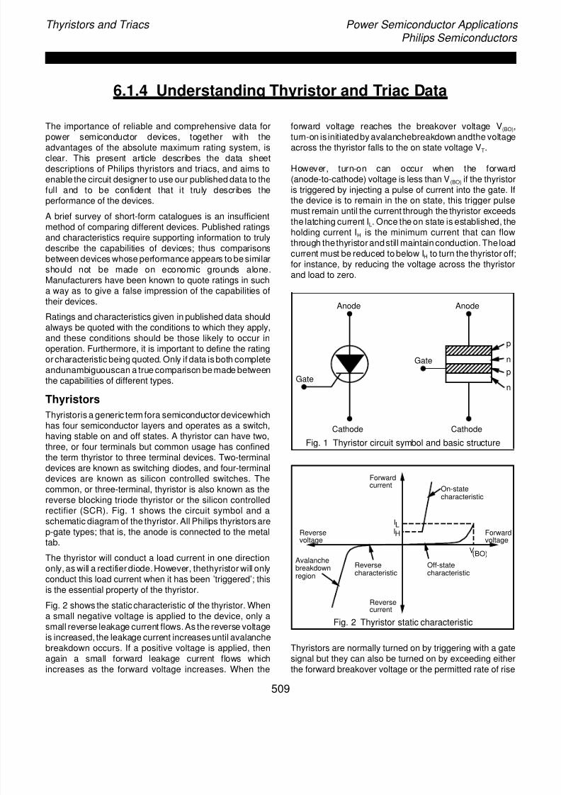
Thyristoris a generic term fora semiconductor devicewhichhas four semiconductor layers and operates as a switch,having stable on and off states. A thyristor can have two,three, or four terminals but common usage has confinedthe term thyristor to three terminal devices. Two-terminaldevices are known as switching diodes, and four-terminaldevices are known as silicon controlled switches. Thecommon, or three-terminal, thyristor is also known as thereverse blocking triode thyristor or the silicon controlledrectifier (SCR). Fig. 1 shows the circuit symbol and aschematic diagram of the thyristor. All Philips thyristors arep-gate types; that is, the anode is connected to the metaltab.
The thyristor will conduct a load current in one directiononly, as will a rectifier diode.However, thethyristor will onlyconduct this load current when it has been ’triggered’; thisis the essential property of the thyristor.
Fig. 2 shows the static characteristic of the thyristor. Whena small negative voltage is applied to the device, only asmall reverse leakage current flows. As the reverse voltageis increased, the leakage current increases until avalanchebreakdown occurs. If a positive voltage is applied, thenagain a small forward leakage current flows whichincreases as the forward voltage increases. When the
forward voltage reaches the breakover voltage V(BO),
turn-on is initiatedby avalanchebreakdown andthe voltageacross the thyristor falls to the on state voltage VT.
However, turn-on can occur when the forward(anode-to-cathode) voltage is less than V(BO) if the thyristoris triggered by injecting a pulse of current into the gate. Ifthe device is to remain in the on state, this trigger pulsemust remain until the current through the thyristor exceedsthe latching current IL. Once the on state is established, theholding current IH is the minimum current that can flowthrough thethyristor andstill maintain conduction. Theloadcurrent must be reduced to below IH to turn the thyristor off;for instance, by reducing the voltage across the thyristor
and load to zero.
Fig. 1 Thyristor circuit symbol and basic structure
Fig. 2 Thyristor static characteristic
Thyristors are normally turned on by triggering with a gatesignal but they can also be turned on by exceeding eitherthe forward breakover voltage or the permitted rate of rise
Anode Anode
Gate
Gate
Cathode Cathode
p
n
p
n
On-statecharacteristic
Off-statecharacteristic
Avalanchebreakdownregion
Reversecharacteristic
Reversecurrent
Forwardcurrent
Reversevoltage
Forwardvoltage
ILIH
V
(BO)
509
7/25/2019 Thyristors and Triacs
http://slidepdf.com/reader/full/thyristors-and-triacs 26/84
Thyristors and Triacs Power Semiconductor Applications Philips Semiconductors
of anode voltage dVD /dt. However, these alternativemethods of switching to the conducting state should beavoided by suitable circuit design.
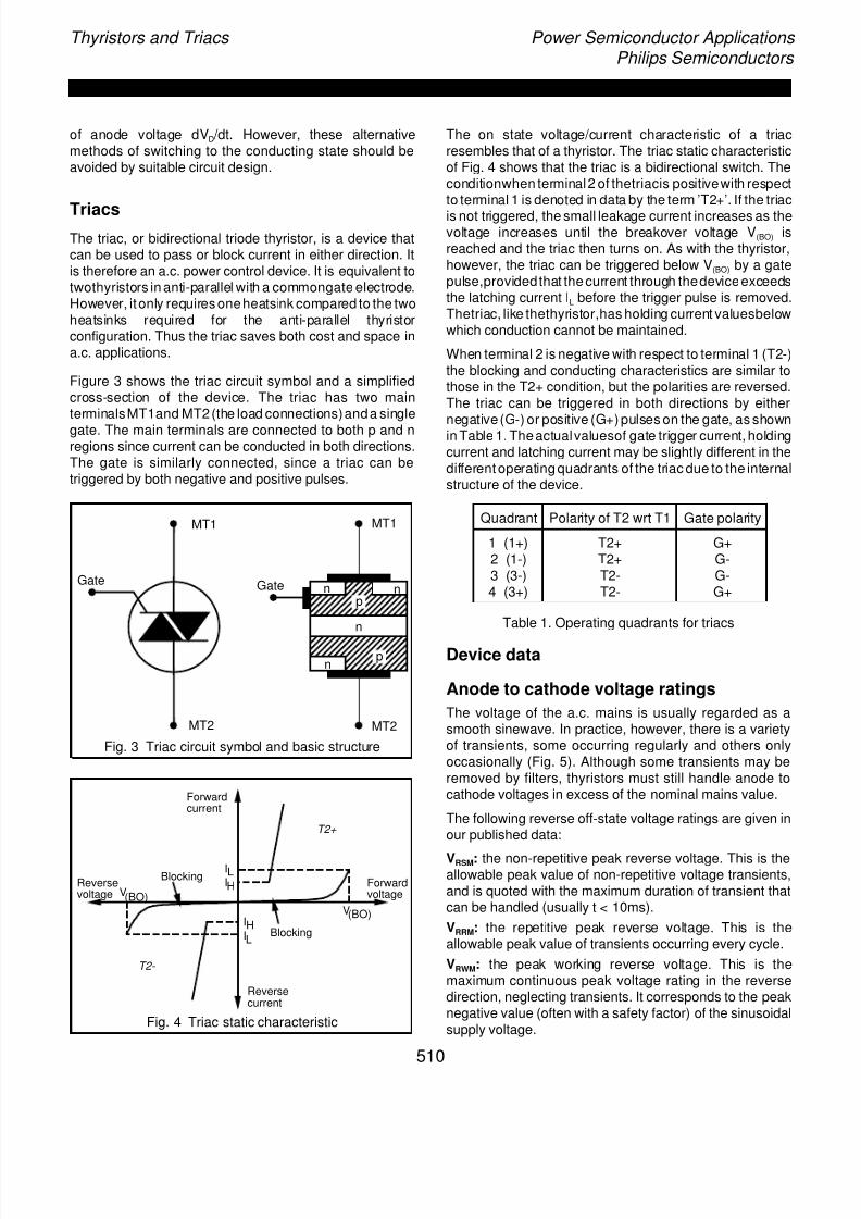
TriacsThe triac, or bidirectional triode thyristor, is a device thatcan be used to pass or block current in either direction. Itis therefore an a.c. power control device. It is equivalent totwothyristors in anti-parallel with a commongate electrode.However, itonly requires oneheatsink compared to the twoheatsinks required for the anti-parallel thyristorconfiguration. Thus the triac saves both cost and space ina.c. applications.
Figure 3 shows the triac circuit symbol and a simplifiedcross-section of the device. The triac has two mainterminalsMT1and MT2(the load connections)anda single
gate. The main terminals are connected to both p and nregions since current can be conducted in both directions.The gate is similarly connected, since a triac can betriggered by both negative and positive pulses.
Fig. 3 Triac circuit symbol and basic structure
Fig. 4 Triac static characteristic
The on state voltage/current characteristic of a triacresembles that of a thyristor. The triac static characteristicof Fig. 4 shows that the triac is a bidirectional switch. Theconditionwhen terminal2 of thetriacis positivewith respectto terminal 1 is denoted in data by the term ’T2+’. If the triac
is not triggered, the small leakage current increases as thevoltage increases until the breakover voltage V(BO) isreached and the triac then turns on. As with the thyristor,however, the triac can be triggered below V(BO) by a gatepulse,providedthat the current through thedeviceexceedsthe latching current IL before the trigger pulse is removed.Thetriac, like thethyristor,has holding current valuesbelowwhich conduction cannot be maintained.
When terminal 2 is negative with respect to terminal 1 (T2-)the blocking and conducting characteristics are similar tothose in the T2+ condition, but the polarities are reversed.The triac can be triggered in both directions by eithernegative (G-) or positive (G+) pulses on the gate, as shownin Table 1. Theactualvaluesof gate trigger current, holdingcurrent and latching current may be slightly different in thedifferent operating quadrants of the triac due to the internalstructure of the device.
Quadrant Polarity of T2 wrt T1 Gate polarity
1 (1+) T2+ G+2 (1-) T2+ G-3 (3-) T2- G-4 (3+) T2- G+
Table 1. Operating quadrants for triacs
Device data
Anode to cathode voltage ratings
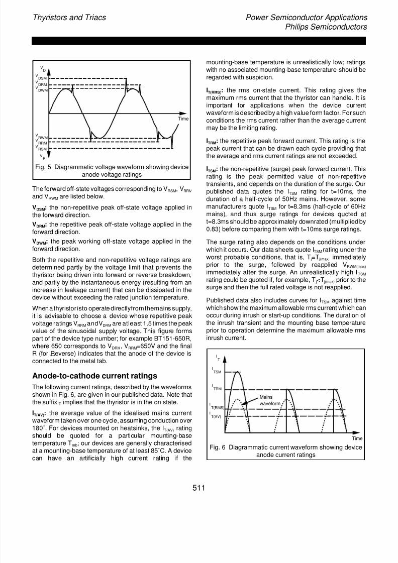
The voltage of the a.c. mains is usually regarded as asmooth sinewave. In practice, however, there is a varietyof transients, some occurring regularly and others onlyoccasionally (Fig. 5). Although some transients may beremoved by filters, thyristors must still handle anode tocathode voltages in excess of the nominal mains value.
The following reverse off-state voltage ratings are given inour published data:
VRSM: the non-repetitive peak reverse voltage. This is theallowable peak value of non-repetitive voltage transients,and is quoted with the maximum duration of transient thatcan be handled (usually t < 10ms).
VRRM: the repetitive peak reverse voltage. This is theallowable peak value of transients occurring every cycle.
VRWM: the peak working reverse voltage. This is themaximum continuous peak voltage rating in the reversedirection, neglecting transients. It corresponds to the peaknegative value (often with a safety factor) of the sinusoidalsupply voltage.
MT1
MT2
Gate Gate
MT1
MT2
n
n
n
n
p
p
Reversecurrent
Forwardcurrent
Reversevoltage
Forwardvoltage
IHIL
V(BO)
Blocking
Blocking
ILIH
V(BO)
T2+
T2-
510
7/25/2019 Thyristors and Triacs
http://slidepdf.com/reader/full/thyristors-and-triacs 27/84
Thyristors and Triacs Power Semiconductor Applications Philips Semiconductors
Fig. 5 Diagrammatic voltage waveform showing deviceanode voltage ratings
The forwardoff-state voltages corresponding to VRSM, VRRM
and VRWM are listed below.VDSM: the non-repetitive peak off-state voltage applied inthe forward direction.
VDRM: the repetitive peak off-state voltage applied in theforward direction.
VDWM: the peak working off-state voltage applied in theforward direction.
Both the repetitive and non-repetitive voltage ratings aredetermined partly by the voltage limit that prevents thethyristor being driven into forward or reverse breakdown,and partly by the instantaneous energy (resulting from anincrease in leakage current) that can be dissipated in the
device without exceeding the rated junction temperature.
Whenathyristor isto operate directlyfromthemains supply,it is advisable to choose a device whose repetitive peakvoltage ratings VRRM andVDRM are atleast 1.5 times the peakvalue of the sinusoidal supply voltage. This figure formspart of the device type number; for example BT151-650R,where 650 corresponds to VDRM, VRRM=650V and the finalR (for Reverse) indicates that the anode of the device isconnected to the metal tab.
Anode-to-cathode current ratings
The following current ratings, described by the waveforms
shown in Fig. 6, are given in our published data. Note thatthe suffix T implies that the thyristor is in the on state.
IT(AV): the average value of the idealised mains currentwaveform taken over one cycle, assuming conduction over180˚. For devices mounted on heatsinks, the IT(AV) ratingshould be quoted for a particular mounting-basetemperature Tmb; our devices are generally characterisedat a mounting-base temperature of at least 85˚C. A devicecan have an artificially high current rating if the
mounting-base temperature is unrealistically low; ratingswith no associated mounting-base temperature should beregarded with suspicion.
IT(RMS): the rms on-state current. This rating gives the
maximum rms current that the thyristor can handle. It isimportant for applications when the device currentwaveformis describedby a high value form factor. Forsuchconditions the rms current rather than the average currentmay be the limiting rating.
ITRM: the repetitive peak forward current. This rating is thepeak current that can be drawn each cycle providing thatthe average and rms current ratings are not exceeded.
ITSM: the non-repetitive (surge) peak forward current. Thisrating is the peak permitted value of non-repetitivetransients, and depends on the duration of the surge. Ourpublished data quotes the ITSM rating for t=10ms, the
duration of a half-cycle of 50Hz mains. However, somemanufacturers quote ITSM for t=8.3ms (half-cycle of 60Hzmains), and thus surge ratings for devices quoted att=8.3ms should be approximately downrated (multiplied by0.83) before comparing them with t=10ms surge ratings.
The surge rating also depends on the conditions underwhich it occurs. Our data sheets quote ITSM rating under theworst probable conditions, that is, T j=T j(max) immediatelyprior to the surge, followed by reapplied VRWM(max)
immediately after the surge. An unrealistically high ITSM
rating could be quoted if, for example, T j<T j(max) prior to thesurge and then the full rated voltage is not reapplied.
Published data also includes curves for ITSM against timewhichshow the maximum allowable rms current which canoccur during inrush or start-up conditions. The duration ofthe inrush transient and the mounting base temperatureprior to operation determine the maximum allowable rmsinrush current.
Fig. 6 Diagrammatic current waveform showing deviceanode current ratings
VD
VDSM
VDRM
VDWM
VRWM
VRRM
VRSM
VR
Time
Mains
waveform
IT
ITSM
ITRM
IT(RMS)
IT(AV)
Time
511
7/25/2019 Thyristors and Triacs
http://slidepdf.com/reader/full/thyristors-and-triacs 28/84
Thyristors and Triacs Power Semiconductor Applications Philips Semiconductors
dI/dt: the rate of rise of on-state current permissible aftertriggering. An excessive rate of rise of current causes localheating and thus damage to the device. The rate of rise ofcurrent is determined by both the supply and loadimpedances, and can be limited by additional series
inductance in the circuit.
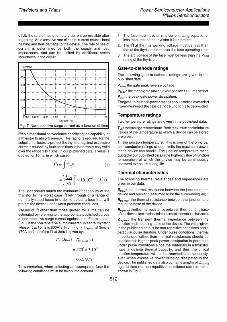
Fig. 7 Non-repetitive surge current as a function of time
I2t: a dimensional convenience specifying the capability ofa thyristor to absorb energy. This rating is required for theselection of fuses to protect the thyristor against excessivecurrents caused by fault conditions. It is normally only validover the range 3 to 10ms. In our published data, a value isquoted for 10ms, in which case:
The user should match the minimum I2t capability of thethyristor to the worst case I2t let-through of a range ofnominally rated fuses in order to select a fuse that willprotect the device under worst probable conditions.
Values of I2t other than those quoted for 10ms can beestimated by referring to the appropriate published curvesof non-repetitive surge current against time. For example,Fig. 7 is thenonrepetitive surge current curve fora thyristorwhose I2t at 10ms is 800A2s. From Fig. 7, ITS(RMS) at 3ms is470A and therefore I2t at 3ms is given by:
To summarise, when selecting an appropriate fuse thefollowing conditions must be taken into account.
1. The fuse must have an rms current rating equal to, orless than, that of the thyristor it is to protect.
2. The I2t at the rms working voltage must be less thanthat of the thyristor taken over the fuse operating time.
3. The arc voltage of the fuse must be less than the VRSM
rating of the thyristor.
Gate-to-cathode ratings
The following gate-to-cathode ratings are given in thepublished data.
VRGM: the gate peak reverse voltage.
PG(AV): the mean gate power, averaged over a 20ms period.
PGM: the peak gate power dissipation.
Thegate-to-cathode power ratings shouldnotbe exceededifover-heatingof thegate-cathodejunctionis tobeavoided.
Temperature ratings
Two temperature ratings are given in the published data.
Tstg: thestorage temperature. Bothmaximumandminimumvalues of the temperature at which a device can be storedare given.
Tj: the junction temperature. This is one of the principalsemiconductor ratings since it limits the maximum powerthat a device can handle. The junction temperature ratingquoted inour published data is the highest value of junctiontemperature at which the device may be continuouslyoperated to ensure a long life.
Thermal characteristics
The following thermal resistances and impedances aregiven in our data.
Rth(j-a): the thermal resistance between the junction of thedevice and ambient (assumed to be the surrounding air).
Rth(j-mb): the thermal resistance between the junction andmounting base of the device.
Rth(mb-h): thethermal resistance between themountingbaseof thedevice and theheatsink (contact thermal resistance).
Zth(j-mb): the transient thermal impedance between the junction and mounting-base of the device. The value givenin the published data is for non-repetitive conditions and aparticular pulse duration. Under pulse conditions, thermalimpedances rather than thermal resistances should beconsidered. Higher peak power dissipation is permittedunder pulse conditions since the materials in a thyristorhave a definite thermal capacity, and thus the critical
junction temperature will not be reached instantaneously,even when excessive power is being dissipated in thedevice. The published data also contains graphs of Zth(j-mb)
against time (for non-repetitive conditions) such as thoseshown in Fig. 8.
0.001 0.003 0.01 0.03 0.1 0.3 1 3 100
100
200
300
400
500
600
Duration (s)
ITS(RMS)
I 2t = ⌠
⌡
i2.dt (1)
=
I TSM
√ 2
2
× 10.10−3 ( A2
s)
I 2t (3ms) = I
TS ( RMS )2 × t
= 4702 × 3.10
−3
= 662.7 A2s
512
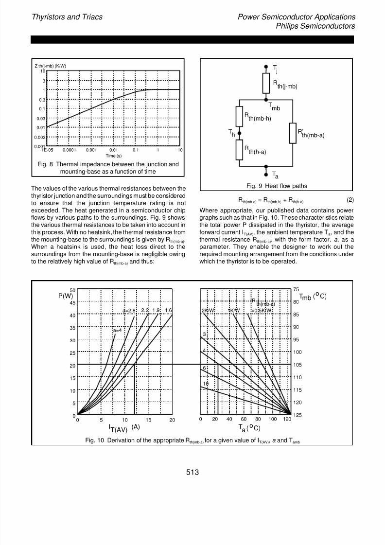
7/25/2019 Thyristors and Triacs
http://slidepdf.com/reader/full/thyristors-and-triacs 29/84
Thyristors and Triacs Power Semiconductor Applications Philips Semiconductors
Fig. 8 Thermal impedance between the junction andmounting-base as a function of time
The values of the various thermal resistances between thethyristor junction and the surroundingsmust be consideredto ensure that the junction temperature rating is notexceeded. The heat generated in a semiconductor chipflows by various paths to the surroundings. Fig. 9 showsthe various thermal resistances to be taken into account inthis process. With no heatsink, the thermal resistance fromthe mounting-base to the surroundings is given by Rth(mb-a).When a heatsink is used, the heat loss direct to thesurroundings from the mounting-base is negligible owingto the relatively high value of Rth(mb-a) and thus:
Fig. 9 Heat flow paths
Rth(mb-a) = Rth(mb-h) + Rth(h-a) (2)
Where appropriate, our published data contains powergraphs such as that in Fig. 10. These characteristics relatethe total power P dissipated in the thyristor, the averageforward current IT(AV), the ambient temperature Ta, and thethermal resistance Rth(mb-a), with the form factor, a , as aparameter. They enable the designer to work out therequired mounting arrangement from the conditions underwhich the thyristor is to be operated.
1E-05 0.0001 0.001 0.01 0.1 1 100.001
0.003
0.01
0.03
0.1
0.3
1
3
10
Time (s)
Z th(j-mb) (K/W) T j
Tmb
Th
Ta
Rth(j-mb)
R’th(mb-a)
Rth(mb-h)
Rth(h-a)
Fig. 10 Derivation of the appropriate Rth(mb-a) for a given value of IT(AV), a and Tamb
0 5 10 15 200
5
10
15
20
25
30
35
40
45
50
0 20 40 60 80 100 120125
120
115
110
105
100
95
90
85
80
75
a=4
a=2.8 2.2 1.9 1.6
Rth(mb-a)
=0.5K/W1K/W2K/W
3
4
6
10
P(W) Tmb (oC)
IT(AV)
(A) Ta ( oC)
513
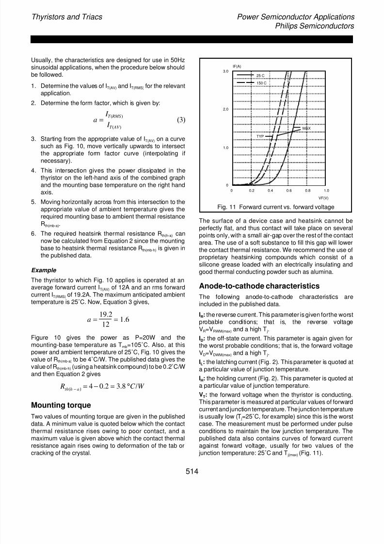
7/25/2019 Thyristors and Triacs
http://slidepdf.com/reader/full/thyristors-and-triacs 30/84
Thyristors and Triacs Power Semiconductor Applications Philips Semiconductors
Usually, the characteristics are designed for use in 50Hzsinusoidal applications, when the procedure below shouldbe followed.
1. Determine the values of IT(AV) and IT(RMS) for the relevant
application.2. Determine the form factor, which is given by:
3. Starting from the appropriate value of IT(AV) on a curvesuch as Fig. 10, move vertically upwards to intersectthe appropriate form factor curve (interpolating ifnecessary).
4. This intersection gives the power dissipated in thethyristor on the left-hand axis of the combined graphand the mounting base temperature on the right hand
axis.
5. Moving horizontally across from this intersection to theappropriate value of ambient temperature gives therequired mounting base to ambient thermal resistanceRth(mb-a).
6. The required heatsink thermal resistance Rth(h-a) cannow be calculated from Equation 2 since the mountingbase to heatsink thermal resistance Rth(mb-h) is given inthe published data.
Example
The thyristor to which Fig. 10 applies is operated at an
average forward current IT(AV) of 12A and an rms forwardcurrent IT(RMS) of 19.2A. The maximum anticipated ambienttemperature is 25˚C. Now, Equation 3 gives,
Figure 10 gives the power as P=20W and themounting-base temperature as Tmb=105˚C. Also, at thispower and ambient temperature of 25˚C, Fig. 10 gives thevalue of Rth(mb-a) to be 4˚C/W. The published data gives thevalue of Rth(mb-h) (usinga heatsink compound) to be 0.2˚C/Wand then Equation 2 gives
Mounting torque
Two values of mounting torque are given in the publisheddata. A minimum value is quoted below which the contactthermal resistance rises owing to poor contact, and amaximum value is given above which the contact thermalresistance again rises owing to deformation of the tab orcracking of the crystal.
Fig. 11 Forward current vs. forward voltage
The surface of a device case and heatsink cannot beperfectly flat, and thus contact will take place on severalpoints only, with a small air-gap over the rest of the contactarea. The use of a soft substance to fill this gap will lowerthe contact thermal resistance. We recommend the use ofproprietary heatsinking compounds which consist of asilicone grease loaded with an electrically insulating andgood thermal conducting powder such as alumina.
Anode-to-cathode characteristicsThe following anode-to-cathode characteristics areincluded in the published data.
IR: the reverse current. This parameter is given forthe worstprobable conditions; that is, the reverse voltageVR=VRWM(max) and a high T j.
ID: the off-state current. This parameter is again given forthe worst probable conditions; that is, the forward voltageVD=VDWM(max) and a high T j.
IL: the latching current (Fig. 2). This parameter is quoted ata particular value of junction temperature.
IH: the holding current (Fig. 2). This parameter is quoted ata particular value of junction temperature.
VT: the forward voltage when the thyristor is conducting.This parameter is measured at particular values of forwardcurrent and junction temperature.The junction temperatureis usually low (T j=25˚C, for example) since this is the worstcase. The measurement must be performed under pulseconditions to maintain the low junction temperature. Thepublished data also contains curves of forward currentagainst forward voltage, usually for two values of the
junction temperature: 25˚C and T j(max) (Fig. 11).
0 0.2 0.4 0.6 0.8 1.0
0
1.0
2.0
3.0
IF(A)
VF(V)
MAX
TYP
25 C
150 C
a = I T ( RMS )
I T ( AV )(3)
a = 19.2
12 = 1.6
Rth(h − a) = 4 − 0.2 = 3.8 °C /W
514
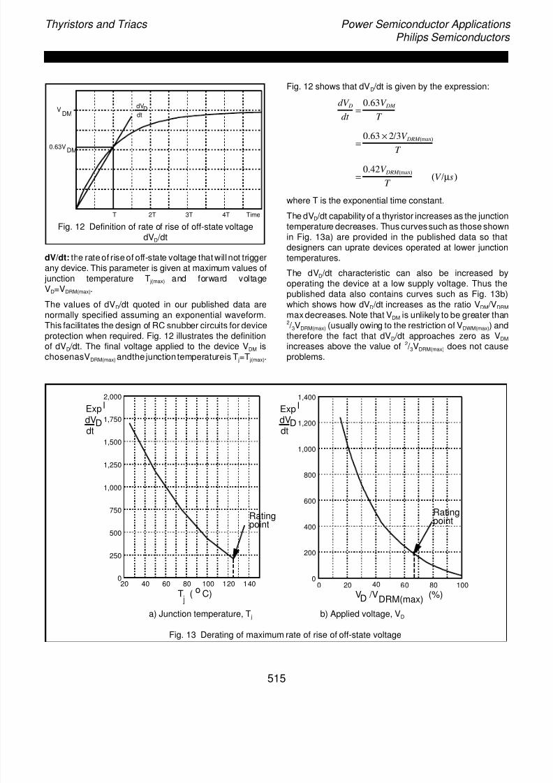
7/25/2019 Thyristors and Triacs
http://slidepdf.com/reader/full/thyristors-and-triacs 31/84
Thyristors and Triacs Power Semiconductor Applications Philips Semiconductors
Fig. 12 Definition of rate of rise of off-state voltagedVD /dt
dV/dt: the rate of rise of off-state voltage that will not triggerany device. This parameter is given at maximum values of
junction temperature T j(max) and forward voltageVD=VDRM(max).
The values of dVD /dt quoted in our published data arenormally specified assuming an exponential waveform.This facilitates the design of RC snubber circuits for deviceprotection when required. Fig. 12 illustrates the definitionof dVD /dt. The final voltage applied to the device VDM ischosenasVDRM(max) andthejunction temperatureis T j=T j(max).
Fig. 12 shows that dVD /dt is given by the expression:
where T is the exponential time constant.
The dVD /dt capability of a thyristor increases as the junctiontemperature decreases. Thus curvessuch as those shownin Fig. 13a) are provided in the published data so thatdesigners can uprate devices operated at lower junctiontemperatures.
The dVD /dt characteristic can also be increased byoperating the device at a low supply voltage. Thus thepublished data also contains curves such as Fig. 13b)which shows how dVD /dt increases as the ratio VDM /VDRM
max decreases. Note that VDM is unlikely to be greater than2 / 3VDRM(max) (usually owing to the restriction of VDWM(max)) andtherefore the fact that dVD /dt approaches zero as VDM
increases above the value of 2 / 3VDRM(max) does not causeproblems.
dVDdt
VDM
0.63VDM
T 2T 3T 4T Time
dV D
dt =
0.63V DM
T
= 0.63 × 2/3V DRM (max)
T
= 0.42V DRM (max)
T (V /µs)
a) Junction temperature, T j b) Applied voltage, VD
Fig. 13 Derating of maximum rate of rise of off-state voltage
0 20 40 60 80 1000
200
400
600
800
1,000
1,200
1,400
Expl
dVDdt
Expl
dVDdt
Ratingpoint
Ratingpoint
T j
( o C) VD /VDRM(max)
(%)
20 40 60 80 100 120 1400
250
500
750
1,000
1,250
1,500
1,750
2,000
515
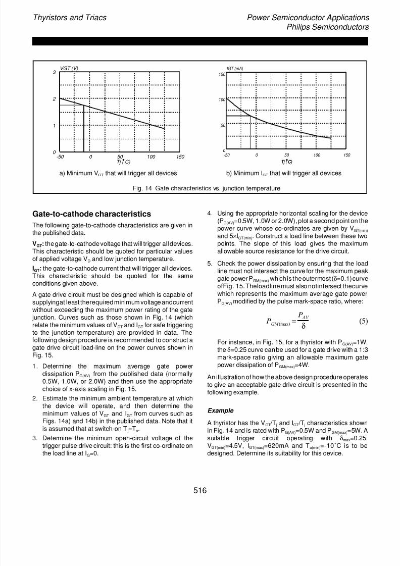
7/25/2019 Thyristors and Triacs
http://slidepdf.com/reader/full/thyristors-and-triacs 32/84
Thyristors and Triacs Power Semiconductor Applications Philips Semiconductors
a) Minimum VGT that will trigger all devices b) Minimum IGT that will trigger all devices
Fig. 14 Gate characteristics vs. junction temperature
-50 0 50 100 150 Tj ( C)
VGT (V)3
2
1
0 0
50
100
150
0 50 100 150 -50
IGT (mA)
Tj ( C)Tj ( C)
Gate-to-cathode characteristics
The following gate-to-cathode characteristics are given inthe published data.
VGT: thegate-to-cathodevoltage that will trigger alldevices.This characteristic should be quoted for particular valuesof applied voltage VD and low junction temperature.
IGT: the gate-to-cathode current that will trigger all devices.This characteristic should be quoted for the sameconditions given above.
A gate drive circuit must be designed which is capable ofsupplyingat least therequiredminimum voltageandcurrentwithout exceeding the maximum power rating of the gate
junction. Curves such as those shown in Fig. 14 (whichrelate the minimum values of VGT and IGT for safe triggeringto the junction temperature) are provided in data. Thefollowing design procedure is recommended to construct agate drive circuit load-line on the power curves shown inFig. 15.
1. Determine the maximum average gate powerdissipation PG(AV) from the published data (normally0.5W, 1.0W, or 2.0W) and then use the appropriatechoice of x-axis scaling in Fig. 15.
2. Estimate the minimum ambient temperature at whichthe device will operate, and then determine theminimum values of VGT and IGT from curves such asFigs. 14a) and 14b) in the published data. Note that itis assumed that at switch-on T j=Ta.
3. Determine the minimum open-circuit voltage of thetrigger pulse drive circuit: this is the first co-ordinate onthe load line at IG=0.
4. Using the appropriate horizontal scaling for the device(PG(AV)=0.5W, 1.0W or 2.0W), plot a second point on thepower curve whose co-ordinates are given by VGT(min)
and 5×IGT(min). Construct a load line between these twopoints. The slope of this load gives the maximumallowable source resistance for the drive circuit.
5. Check the power dissipation by ensuring that the loadline must not intersect the curve for the maximum peakgate powerPGM(max) which is theoutermost (δ=0.1)curveofFig. 15.Theloadlinemust also notintersect thecurvewhich represents the maximum average gate powerPG(AV) modified by the pulse mark-space ratio, where:
For instance, in Fig. 15, for a thyristor with PG(AV)=1W,the δ=0.25 curve canbe used for a gate drive with a 1:3mark-space ratio giving an allowable maximum gatepower dissipation of PGM(max)=4W.
An illustration of how the above design procedure operatesto give an acceptable gate drive circuit is presented in thefollowing example.
Example
A thyristor has the VGT /T j and IGT /T j characteristics shownin Fig. 14 and is rated with PG(AV)=0.5W and PGM(max)=5W. Asuitable trigger circuit operating with δmax=0.25,VGT(min)=4.5V, IGT(max)=620mA and Ta(min)=-10˚C is to bedesigned. Determine its suitability for this device.
PGM (max) =
P AV
δ (5)
516
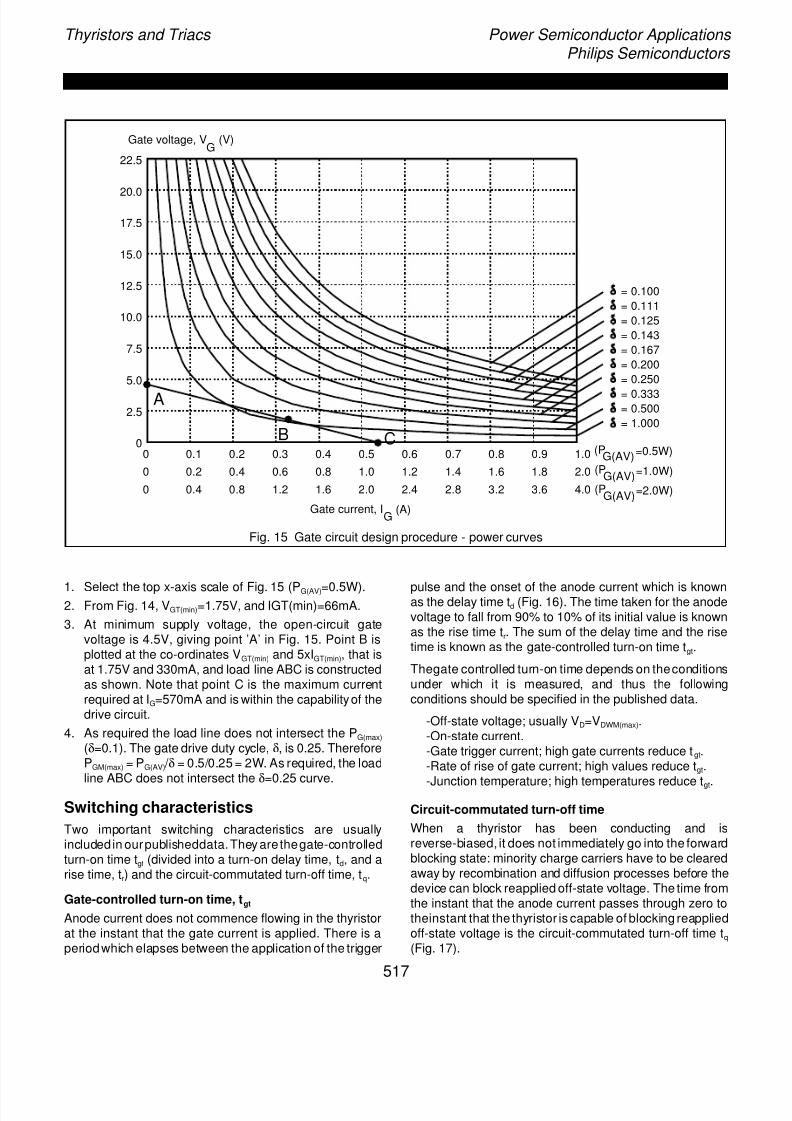
7/25/2019 Thyristors and Triacs
http://slidepdf.com/reader/full/thyristors-and-triacs 33/84
Thyristors and Triacs Power Semiconductor Applications Philips Semiconductors
Fig. 15 Gate circuit design procedure - power curves
0
2.5
5.0
7.5
10.0
12.5
15.0
17.5
20.0
22.5
0 0.1 0.2 0.3 0.4 0.5 0.6 0.7 0.8 0.9 1.0
0 0.2 0.4 0.6 0.8 1.0 1.2 1.4 1.6 1.8 2.0
0 0.4 0.8 1.2 1.6 2.0 2.4 2.8 3.2 3.6 4.0
= 0.100
= 0.111
= 0.125
= 0.143
= 0.167
= 0.200
= 0.250
= 0.333= 0.500
= 1.000
Gate current, IG
(A)
Gate voltage, VG
(V)
(PG(AV)=0.5W)
(PG(AV)=1.0W)
(PG(AV)=2.0W)
A
B C
1. Select the top x-axis scale of Fig. 15 (PG(AV)=0.5W).2. From Fig. 14, VGT(min)=1.75V, and IGT(min)=66mA.
3. At minimum supply voltage, the open-circuit gatevoltage is 4.5V, giving point ’A’ in Fig. 15. Point B isplotted at the co-ordinates VGT(min) and 5xIGT(min), that isat 1.75V and 330mA, and load line ABC is constructedas shown. Note that point C is the maximum currentrequired at IG=570mA and is within the capabilityof thedrive circuit.
4. As required the load line does not intersect the PG(max)
(δ=0.1). The gate drive duty cycle, δ, is 0.25. ThereforePGM(max) = PG(AV) / δ = 0.5/0.25 = 2W. As required, the loadline ABC does not intersect the
δ=0.25 curve.
Switching characteristics
Two important switching characteristics are usuallyincludedin ourpublisheddata.They arethegate-controlledturn-on time tgt (divided into a turn-on delay time, td, and arise time, tr) and the circuit-commutated turn-off time, tq.
Gate-controlled turn-on time, tgt
Anode current does not commence flowing in the thyristorat the instant that the gate current is applied. There is aperiodwhich elapses between the application of the trigger
pulse and the onset of the anode current which is knownas the delay time td (Fig. 16). The time taken for the anodevoltage to fall from 90% to 10% of its initial value is knownas the rise time tr. The sum of the delay time and the risetime is known as the gate-controlled turn-on time tgt.
Thegate controlled turn-on time depends on theconditionsunder which it is measured, and thus the followingconditions should be specified in the published data.
-Off-state voltage; usually VD=VDWM(max).-On-state current.-Gate trigger current; high gate currents reduce tgt.-Rate of rise of gate current; high values reduce tgt.
-Junction temperature; high temperatures reduce tgt.
Circuit-commutated turn-off time
When a thyristor has been conducting and isreverse-biased, it does not immediately go into the forwardblocking state: minority charge carriers have to be clearedaway by recombination and diffusion processes before thedevice can block reapplied off-state voltage. The time fromthe instant that the anode current passes through zero totheinstant that the thyristor is capable of blocking reappliedoff-state voltage is the circuit-commutated turn-off time tq
(Fig. 17).
517
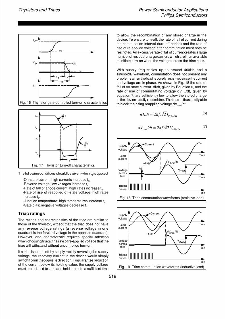
7/25/2019 Thyristors and Triacs
http://slidepdf.com/reader/full/thyristors-and-triacs 34/84
Thyristors and Triacs Power Semiconductor Applications Philips Semiconductors
Fig. 16 Thyristor gate-controlled turn-on characteristics
Fig. 17 Thyristor turn-off characteristics
The followingconditions should be given when tq is quoted.
-On-state current; high currents increase tq.-Reverse voltage; low voltages increase tq.-Rate of fall of anode current; high rates increase tq.-Rate of rise of reapplied off-state voltage; high ratesincrease tq.-Junction temperature; high temperatures increase tq.-Gate bias; negative voltages decrease tq.
Triac ratings
The ratings and characteristics of the triac are similar to
those of the thyristor, except that the triac does not haveany reverse voltage ratings (a reverse voltage in onequadrant is the forward voltage in the opposite quadrant).However, one characteristic requires special attentionwhen choosing triacs; the rate of re-applied voltage that thetriac will withstand without uncontrolled turn-on.
If a triac is turned off by simply rapidly reversing the supplyvoltage, the recovery current in the device would simplyswitchit on in theopposite direction. Toguarantee reductionof the current below its holding value, the supply voltagemust be reduced to zero and held there for a sufficient time
to allow the recombination of any stored charge in thedevice. To ensure turn-off, the rate of fall of current duringthe commutation interval (turn-off period) and the rate ofrise of re-applied voltage after commutation must both berestricted.Anexcessiverate of fall of current creates a large
numberof residual chargecarriers which arethen availableto initiate turn-on when the voltage across the triac rises.
With supply frequencies up to around 400Hz and asinusoidal waveform, commutation does not present anyproblemswhen theload is purelyresistive, since thecurrentand voltage are in phase. As shown in Fig. 18 the rate offall of on-state current -dI/dt, given by Equation 6, and therate of rise of commutating voltage dVcom /dt, given byequation 7, are sufficiently low to allow the stored chargein the device to fully recombine. The triac is thus easilyableto block the rising reapplied voltage dVcom /dt.
(6)
(7)
Fig. 18 Triac commutation waveforms (resistive load)
Fig. 19 Triac commutation waveforms (inductive load)
90%
10%
10%
V D
I GT
IT
t rt d
tgt
dI /dt = 2π f .√ 2 I T ( RMS )
tq
IT
IR
VD
VR
dIT
dt
dVD
dt
dV com/dt = 2π f .√ 2 V ( RMS )
VDWM
-dI/dt dV
com /dt
Time
Time
Time
Supply
voltage
Loadcurrent
Voltageacrosstriac
Trigger
pulses
Current
VT
VDWM
-dI/dtdV
com /dt
Time
Time
Time
Supply
voltage
Loadcurrent
Voltageacrosstriac
Trigger
pulses
Current
518
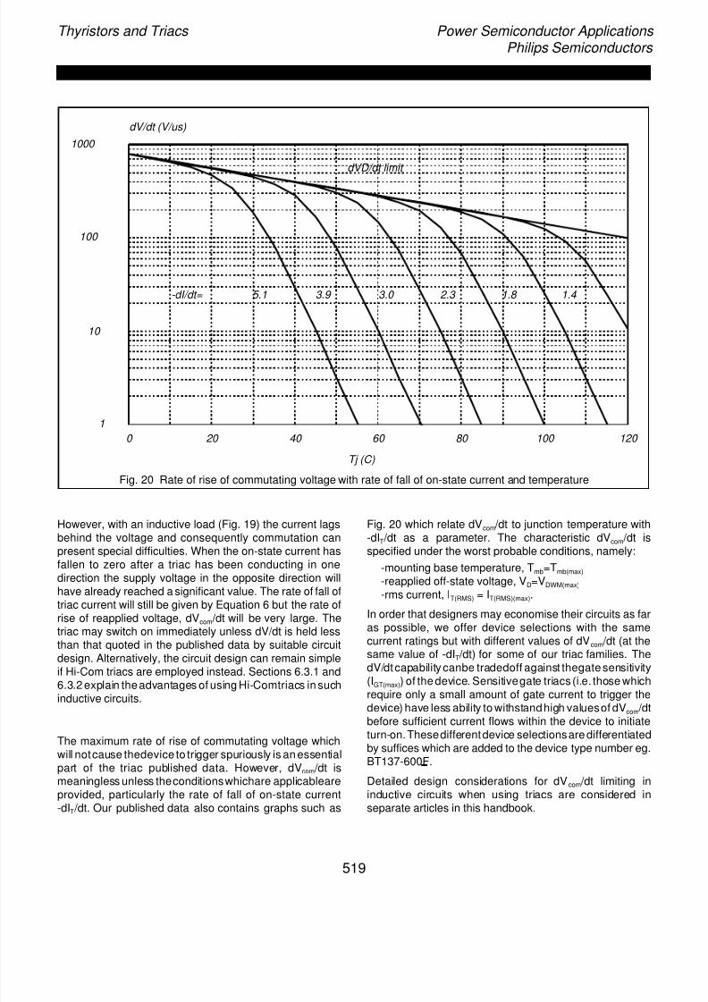
7/25/2019 Thyristors and Triacs
http://slidepdf.com/reader/full/thyristors-and-triacs 35/84
Thyristors and Triacs Power Semiconductor Applications Philips Semiconductors
Fig. 20 Rate of rise of commutating voltage with rate of fall of on-state current and temperature
20 40 60 80 100 1200
1
10
100
1000
dV/dt (V/us)
5.1 3.9 3.0 2.3 1.8 1.4 -dI/dt=
dVD/dt limit
Tj (C)
However, with an inductive load (Fig. 19) the current lagsbehind the voltage and consequently commutation canpresent special difficulties. When the on-state current hasfallen to zero after a triac has been conducting in onedirection the supply voltage in the opposite direction willhave already reached a significant value. The rate of fall oftriac current will still be given by Equation 6 but the rate ofrise of reapplied voltage, dVcom /dt will be very large. Thetriac may switch on immediately unless dV/dt is held lessthan that quoted in the published data by suitable circuitdesign. Alternatively, the circuit design can remain simpleif Hi-Com triacs are employed instead. Sections 6.3.1 and6.3.2 explain theadvantages of using Hi-Comtriacs in such
inductive circuits.
The maximum rate of rise of commutating voltage whichwill notcause thedevice to trigger spuriously is an essentialpart of the triac published data. However, dVcom /dt ismeaningless unless theconditionswhichare applicableareprovided, particularly the rate of fall of on-state current-dIT /dt. Our published data also contains graphs such as
Fig. 20 which relate dVcom /dt to junction temperature with-dIT /dt as a parameter. The characteristic dVcom /dt isspecified under the worst probable conditions, namely:
-mounting base temperature, Tmb=Tmb(max)
-reapplied off-state voltage, VD=VDWM(max)
-rms current, IT(RMS) = IT(RMS)(max).
In order that designers may economise their circuits as faras possible, we offer device selections with the samecurrent ratings but with different values of dVcom /dt (at thesame value of -dIT /dt) for some of our triac families. ThedV/dtcapability canbe tradedoff against thegate sensitivity(IGT(max)) of the device. Sensitivegate triacs (i.e. those whichrequire only a small amount of gate current to trigger thedevice) have less ability to withstandhigh valuesof dVcom /dtbefore sufficient current flows within the device to initiateturn-on.Thesedifferentdevice selectionsare differentiatedby suffices which are added to the device type number eg.BT137-600F.
Detailed design considerations for dVcom /dt limiting ininductive circuits when using triacs are considered inseparate articles in this handbook.
519

7/25/2019 Thyristors and Triacs
http://slidepdf.com/reader/full/thyristors-and-triacs 36/84

7/25/2019 Thyristors and Triacs
http://slidepdf.com/reader/full/thyristors-and-triacs 37/84
Thyristors and Triacs Power Semiconductor Applications Philips Semiconductors
Thyristor and Triac Applications
521

7/25/2019 Thyristors and Triacs
http://slidepdf.com/reader/full/thyristors-and-triacs 38/84
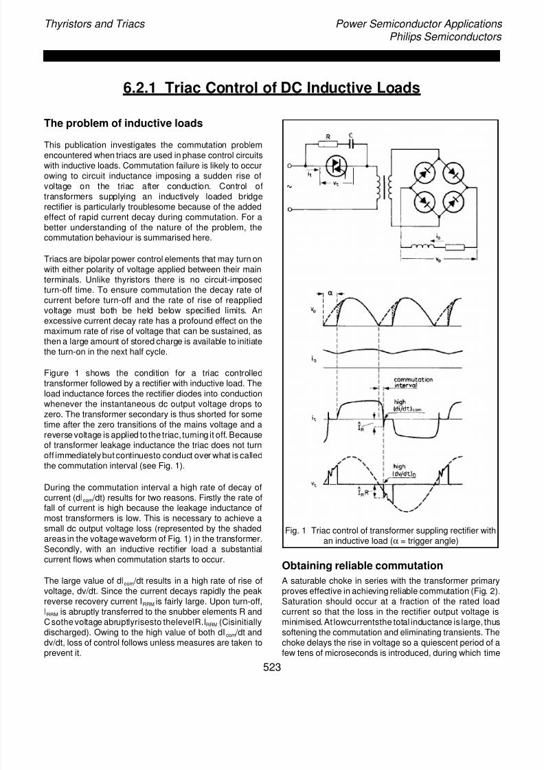
7/25/2019 Thyristors and Triacs
http://slidepdf.com/reader/full/thyristors-and-triacs 39/84
Thyristors and Triacs Power Semiconductor Applications Philips Semiconductors
6.2.1 Triac Control of DC Inductive Loads
The problem of inductive loads
This publication investigates the commutation problemencountered when triacs are used in phase control circuitswith inductive loads. Commutation failure is likely to occurowing to circuit inductance imposing a sudden rise ofvoltage on the triac after conduction. Control oftransformers supplying an inductively loaded bridgerectifier is particularly troublesome because of the addedeffect of rapid current decay during commutation. For abetter understanding of the nature of the problem, thecommutation behaviour is summarised here.
Triacs are bipolar power control elements that may turn on
with either polarity of voltage applied between their mainterminals. Unlike thyristors there is no circuit-imposedturn-off time. To ensure commutation the decay rate ofcurrent before turn-off and the rate of rise of reappliedvoltage must both be held below specified limits. Anexcessive current decay rate has a profound effect on themaximum rate of rise of voltage that can be sustained, asthen a large amount of stored charge is available to initiatethe turn-on in the next half cycle.
Figure 1 shows the condition for a triac controlledtransformer followed by a rectifier with inductive load. Theload inductance forces the rectifier diodes into conduction
whenever the instantaneous dc output voltage drops tozero. The transformer secondary is thus shorted for sometime after the zero transitions of the mains voltage and areverse voltage is applied to the triac, turning it off. Becauseof transformer leakage inductance the triac does not turnoff immediatelybut continuesto conduct over what is calledthe commutation interval (see Fig. 1).
During the commutation interval a high rate of decay ofcurrent (dIcom /dt) results for two reasons. Firstly the rate offall of current is high because the leakage inductance ofmost transformers is low. This is necessary to achieve asmall dc output voltage loss (represented by the shaded
areas in the voltage waveform of Fig. 1) in the transformer.Secondly, with an inductive rectifier load a substantialcurrent flows when commutation starts to occur.
The large value of dIcom /dt results in a high rate of rise ofvoltage, dv/dt. Since the current decays rapidly the peakreverse recovery current IRRM is fairly large. Upon turn-off,IRRM is abruptly transferred to the snubber elements R andCsothe voltage abruptlyrisesto thelevelR.IRRM (Cisinitiallydischarged). Owing to the high value of both dI com /dt anddv/dt, loss of control follows unless measures are taken toprevent it.
Fig. 1 Triac control of transformer suppling rectifier with
an inductive load (α = trigger angle)
Obtaining reliable commutation
A saturable choke in series with the transformer primaryproves effective in achieving reliable commutation (Fig. 2).Saturation should occur at a fraction of the rated loadcurrent so that the loss in the rectifier output voltage isminimised. At lowcurrentsthe total inductance is large, thussoftening the commutation and eliminating transients. Thechoke delays the rise in voltage so a quiescent period of afew tens of microseconds is introduced, during which time
523
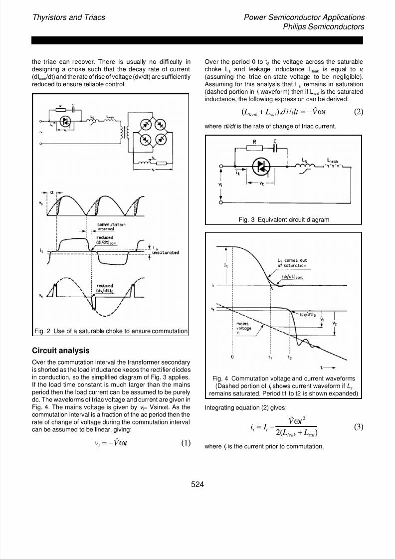
7/25/2019 Thyristors and Triacs
http://slidepdf.com/reader/full/thyristors-and-triacs 40/84
Thyristors and Triacs Power Semiconductor Applications Philips Semiconductors
the triac can recover. There is usually no difficulty indesigning a choke such that the decay rate of current(dIcom /dt)and the rate of rise of voltage(dv/dt) are sufficientlyreduced to ensure reliable control.
Fig. 2 Use of a saturable choke to ensure commutation
Circuit analysis
Over the commutation interval the transformer secondaryis shorted as the load inductance keeps the rectifier diodesin conduction, so the simplified diagram of Fig. 3 applies.If the load time constant is much larger than the mains
period then the load current can be assumed to be purelydc. The waveforms of triac voltage and current are given inFig. 4. The mains voltage is given by v i= Vsinωt. As thecommutation interval is a fraction of the ac period then therate of change of voltage during the commutation intervalcan be assumed to be linear, giving:
Over the period 0 to t2 the voltage across the saturablechoke Ls and leakage inductance Lleak is equal to v i(assuming the triac on-state voltage to be negligible).Assuming for this analysis that Ls remains in saturation(dashed portion in i t waveform) then if Lsat is the saturated
inductance, the following expression can be derived:
where di/dt is the rate of change of triac current.
Fig. 3 Equivalent circuit diagram
Fig. 4 Commutation voltage and current waveforms(Dashed portion of I t shows current waveform if Ls
remains saturated. Period t1 to t2 is shown expanded)
Integrating equation (2) gives:
where I t is the current prior to commutation.
( Lleak + Lsat ).di /dt = − ˆ V ωt (2)
it = I t − ˆ V ωt
2
2( Lleak + Lsat ) (3)
vi = − ˆ V ωt (1)
524
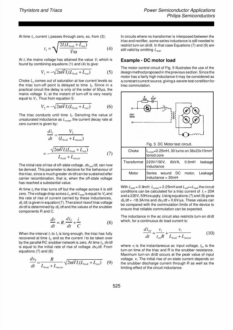
7/25/2019 Thyristors and Triacs
http://slidepdf.com/reader/full/thyristors-and-triacs 41/84
Thyristors and Triacs Power Semiconductor Applications Philips Semiconductors
At time t 1, current i t passes through zero, so, from (3):
At t 1 the mains voltage has attained the value V 1 which isfound by combining equations (1) and (4) to give:
Choke Ls comes out of saturation at low current levels sothe triac turn-off point is delayed to time t 2 . Since in apractical circuit the delay is only of the order of 50µs, themains voltage V 2 at the instant of turn-off is very nearlyequal to V 1. Thus from equation 5:
The triac conducts until time t 2 . Denoting the value ofunsaturated inductance as Lunsat , the current decay rate atzero current is given by:
The initial rate of rise of off-state voltage, dv com /dt , can nowbe derived. This parameter is decisive for the behaviour of
the triac, since a much greater dv/dt can be sustained aftercarrier recombination, that is, when the off-state voltagehas reached a substantial value.
At time t 2 the triac turns off but the voltage across it is stillzero. The voltage drop across Ls and Lleak is equal to V 2 andthe rate of rise of current carried by these inductances,di L /dt , is given in equation(7).Therateof riseof triac voltagedv/dt is determined by di L /dt and the values of the snubbercomponents R and C.
When the interval t 1 to t 2 is long enough, the triac has fullyrecovered at time t 2 , and so the current i to be taken overby the parallel RC snubber network is zero. At time t 2 , dv/dt is equal to the initial rate of rise of voltage dv 0 /dt . Fromequations (7) and (8):
In circuits where no transformer is interposed between thetriac and rectifier, some series inductance is still needed torestrict turn-on di/dt. In that case Equations (7) and (9) arestill valid by omitting Lleak .
Example - DC motor load
The motor control circuit of Fig. 5 illustrates the use of thedesign method proposed in the previous section. Since themotor has a fairly high inductance it may be considered asa constant current source, givinga severe test condition fortriac commutation.
Fig. 5 DC Motor test circuit.
Choke Lunsat=2.25mH, 30 turns on 36x23x10mm3
toriod core
Transformer 220V/150V, 6kVA, 0.9mH leakageinductance
Motor Series wound DC motor, Leakageinductance = 30mH
With Lleak = 0.9mH, Lunsat = 2.25mH and Lsat <<Lleak the circuitconditions can be calculated for a triac current of I t = 20Aand a 220V, 50Hzsupply. Using equations (7) and (9) givesdi c /dt = -18.3A/ms and dv 0 /dt = 0.6V/ µs. These values canbe compared with the commutation limits of the device toensure that reliable commutation can be expected.
The inductance in the ac circuit also restricts turn-on di/dtwhich, for a continuous dc load current is:
where v i is the instantaneous ac input voltage, t on is theturn-on time of the triac and R is the snubber resistance.Maximum turn-on di/dt occurs at the peak value of inputvoltage, v i . The initial rise of on-state current depends onthe snubber discharge current through R as well as thelimiting effect of the circuit inductance.
t 1 =√ 2 I t ( Lleak + Lsat )ˆ V ω
(4)
V 1 = −√ 2ω ˆ VI t ( Lleak + Lsat ) (5)
V 2 ≈ −√ 2ω ˆ VI t ( Lleak + Lsat ) (6)
dic
dt =
V 2
( Lleak + Lunsat )
= −√ 2ω ˆ VI t ( Lleak + Lsat ) Lleak + Lunsat
(7)
dv
dt = R.
di L
dt +
i
C (8)
dion
dt ≈ vi
t on R + vi
Lleak + Lunsat (10)
dv0
dt =
R
Lleak + Lunsat √ 2ω ˆ VI t ( Lleak + Lsat ) (9)
525
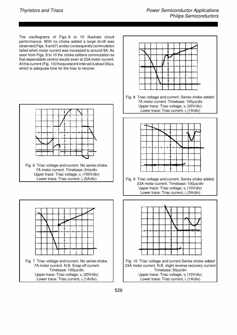
7/25/2019 Thyristors and Triacs
http://slidepdf.com/reader/full/thyristors-and-triacs 42/84
Thyristors and Triacs Power Semiconductor Applications Philips Semiconductors
The oscillograms of Figs. 6 to 10 illustrate circuitperformance. With no choke added a large dv/dt wasobserved(Figs. 6 and7) andso consequentlycommutationfailed when motor current was increased to around 9A. Asseen from Figs. 8 to 10 the choke softens commutation so
that dependable control results even at 23A motor current.At this current (Fig. 10) thequiescent interval is about30µs,which is adequate time for the triac to recover.
Fig. 6 Triac voltage and current. No series choke.7A motor current. Timebase: 2ms/div
Upper trace: Triac voltage, vt (100V/div)Lower trace: Triac current, it (5A/div)
Fig. 7 Triac voltage and current. No series choke.7A motor current. N.B. Snap-off current
Timebase: 100µs/divUpper trace: Triac voltage, vt (20V/div)Lower trace: Triac current, it (1A/div)
Fig. 8 Triac voltage and current. Series choke added.7A motor current. Timebase: 100µs/divUpper trace: Triac voltage, vt (20V/div)Lower trace: Triac current, it (1A/div)
Fig. 9 Triac voltage and current. Series choke added.23A motor current. Timebase: 100µs/divUpper trace: Triac voltage, vt (10V/div)Lower trace: Triac current, it (5A/div)
Fig. 10 Triac voltage and current.Series choke added23A motor current. N.B. slight reverse recovery current
Timebase: 50µs/divUpper trace: Triac voltage, vt (10V/div)Lower trace: Triac current, it (1A/div)
526
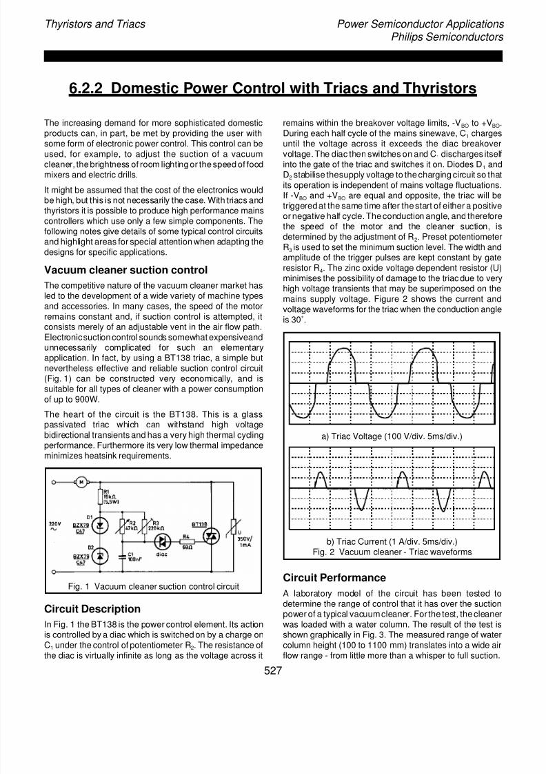
7/25/2019 Thyristors and Triacs
http://slidepdf.com/reader/full/thyristors-and-triacs 43/84
Thyristors and Triacs Power Semiconductor Applications Philips Semiconductors
6.2.2 Domestic Power Control with Triacs and Thyristors
The increasing demand for more sophisticated domestic
products can, in part, be met by providing the user withsome form of electronic power control. This control can beused, for example, to adjust the suction of a vacuumcleaner, the brightness of room lighting or the speed of foodmixers and electric drills.
It might be assumed that the cost of the electronics wouldbe high, but this is not necessarily the case. With triacs andthyristors it is possible to produce high performance mainscontrollers which use only a few simple components. Thefollowing notes give details of some typical control circuitsand highlight areas for special attention when adapting thedesigns for specific applications.
Vacuum cleaner suction controlThe competitive nature of the vacuum cleaner market hasled to the development of a wide variety of machine typesand accessories. In many cases, the speed of the motorremains constant and, if suction control is attempted, itconsists merely of an adjustable vent in the air flow path.Electronicsuction control sounds somewhat expensiveandunnecessarily complicated for such an elementaryapplication. In fact, by using a BT138 triac, a simple butnevertheless effective and reliable suction control circuit(Fig. 1) can be constructed very economically, and issuitable for all types of cleaner with a power consumptionof up to 900W.
The heart of the circuit is the BT138. This is a glasspassivated triac which can withstand high voltagebidirectional transients and has a very high thermal cyclingperformance. Furthermore its very low thermal impedanceminimizes heatsink requirements.
Fig. 1 Vacuum cleaner suction control circuit
Circuit Description
In Fig. 1 the BT138 is the power control element. Its actionis controlled by a diac which is switched on by a charge onC1 under the control of potentiometer R2. The resistance ofthe diac is virtually infinite as long as the voltage across it
remains within the breakover voltage limits, -VBO to +VBO.
During each half cycle of the mains sinewave, C1 chargesuntil the voltage across it exceeds the diac breakovervoltage. The diac then switches on and C1 discharges itselfinto the gate of the triac and switches it on. Diodes D1 andD2 stabilise thesupply voltage to the charging circuit so thatits operation is independent of mains voltage fluctuations.If -VBO and +VBO are equal and opposite, the triac will betriggeredat the same time after thestart of either a positiveor negative half cycle. The conduction angle, and thereforethe speed of the motor and the cleaner suction, isdetermined by the adjustment of R2. Preset potentiometerR3 is used to set the minimum suction level. The width andamplitude of the trigger pulses are kept constant by gate
resistor R4. The zinc oxide voltage dependent resistor (U)minimises the possibility of damage to the triac due to veryhigh voltage transients that may be superimposed on themains supply voltage. Figure 2 shows the current andvoltage waveforms for the triac when the conduction angleis 30˚.
a) Triac Voltage (100 V/div. 5ms/div.)
b) Triac Current (1 A/div. 5ms/div.)Fig. 2 Vacuum cleaner - Triac waveforms
Circuit Performance
A laboratory model of the circuit has been tested todetermine the range of control that it has over the suctionpower of a typical vacuumcleaner. For the test, the cleanerwas loaded with a water column. The result of the test isshown graphically in Fig. 3. The measured range of watercolumn height (100 to 1100 mm) translates into a wide airflow range - from little more than a whisper to full suction.
527
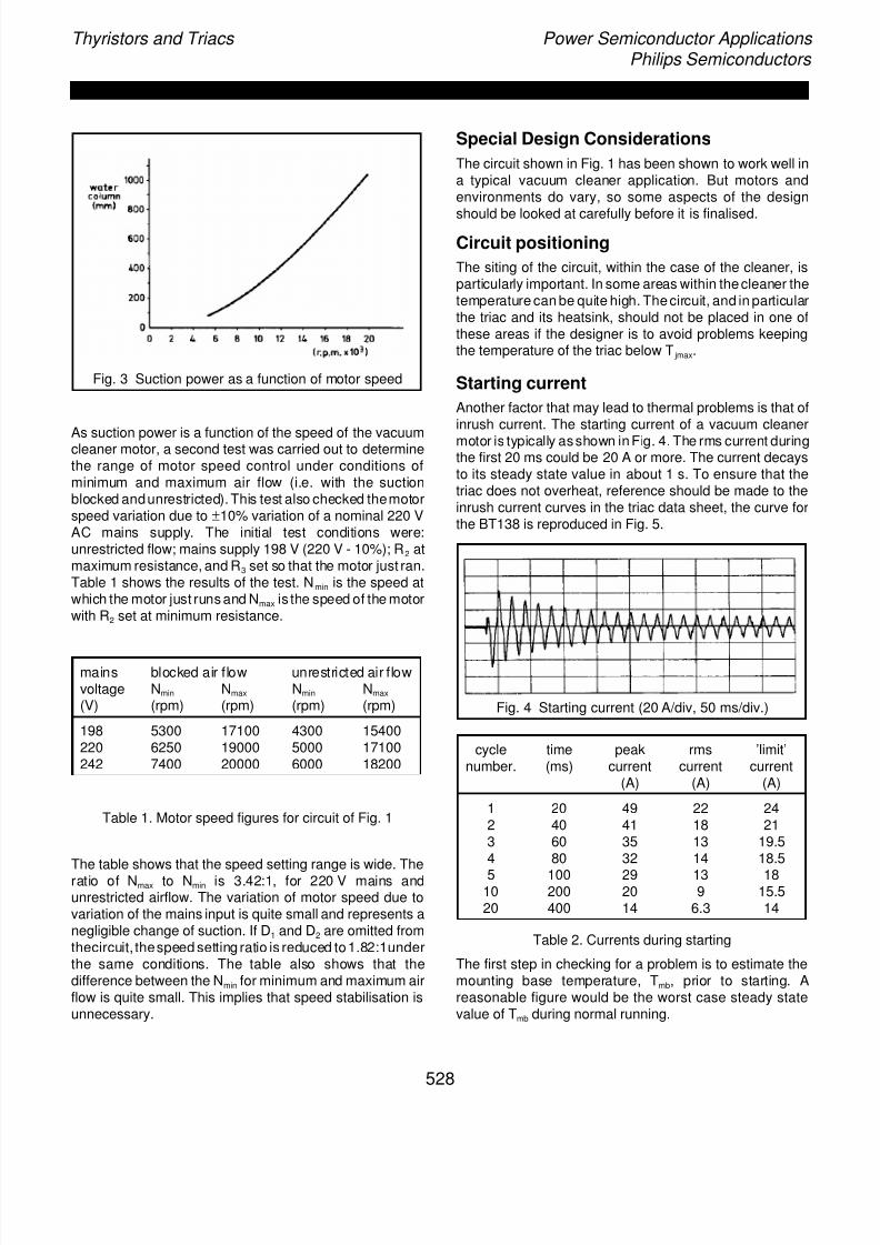
7/25/2019 Thyristors and Triacs
http://slidepdf.com/reader/full/thyristors-and-triacs 44/84
Thyristors and Triacs Power Semiconductor Applications Philips Semiconductors
Fig. 3 Suction power as a function of motor speed
As suction power is a function of the speed of the vacuumcleaner motor, a second test was carried out to determinethe range of motor speed control under conditions ofminimum and maximum air flow (i.e. with the suctionblocked andunrestricted). This test also checked themotorspeed variation due to ±10% variation of a nominal 220 VAC mains supply. The initial test conditions were:unrestricted flow; mains supply 198 V (220 V - 10%); R2 atmaximum resistance, and R3 set so that the motor just ran.Table 1 shows the results of the test. Nmin is the speed atwhich the motor just runs and Nmax is the speed of the motorwith R2 set at minimum resistance.
mains blocked air flow unrestricted air flowvoltage Nmin Nmax Nmin Nmax
(V) (rpm) (rpm) (rpm) (rpm)
198 5300 17100 4300 15400220 6250 19000 5000 17100242 7400 20000 6000 18200
Table 1. Motor speed figures for circuit of Fig. 1
The table shows that the speed setting range is wide. Theratio of Nmax to Nmin is 3.42:1, for 220 V mains andunrestricted airflow. The variation of motor speed due tovariation of the mains input is quite small and represents anegligible change of suction. If D1 and D2 are omitted fromthecircuit, thespeed setting ratio is reduced to1.82:1underthe same conditions. The table also shows that thedifference between the Nmin for minimum and maximum airflow is quite small. This implies that speed stabilisation isunnecessary.
Special Design Considerations
The circuit shown in Fig. 1 has been shown to work well ina typical vacuum cleaner application. But motors andenvironments do vary, so some aspects of the design
should be looked at carefully before it is finalised.
Circuit positioning
The siting of the circuit, within the case of the cleaner, isparticularly important. In some areas within the cleaner thetemperature can be quite high. The circuit, and in particularthe triac and its heatsink, should not be placed in one ofthese areas if the designer is to avoid problems keepingthe temperature of the triac below T jmax.
Starting current
Another factor that may lead to thermal problems is that ofinrush current. The starting current of a vacuum cleaner
motor is typically asshown in Fig. 4. The rms current duringthe first 20 ms could be 20 A or more. The current decaysto its steady state value in about 1 s. To ensure that thetriac does not overheat, reference should be made to theinrush current curves in the triac data sheet, the curve forthe BT138 is reproduced in Fig. 5.
Fig. 4 Starting current (20 A/div, 50 ms/div.)
cycle time peak rms ’limit’number. (ms) current current current
(A) (A) (A)
1 20 49 22 242 40 41 18 213 60 35 13 19.54 80 32 14 18.5
5 100 29 13 1810 200 20 9 15.520 400 14 6.3 14
Table 2. Currents during starting
The first step in checking for a problem is to estimate themounting base temperature, Tmb, prior to starting. Areasonable figure would be the worst case steady statevalue of Tmb during normal running.
528
7/25/2019 Thyristors and Triacs
http://slidepdf.com/reader/full/thyristors-and-triacs 45/84
Thyristors and Triacs Power Semiconductor Applications Philips Semiconductors
Fig. 5 Inrush current curve for BT138
Step 2 is to calculate the rms value of one cycle of thestarting current at several times during start up and step 3is to compare these figures with the values taken from theappropriate line of the inrush current curve.
As an example consider the performance of the BT138driving a motor whose starting current is shown in Fig. 4.Direct measurement indicated that during normal runningthe Tmb of a BT138 mounted on a particular heatsink, wouldbe no more than 22˚C above ambient. From othermeasurements it was estimated that the ambienttemperature would not exceed 73˚C. These figures give aworst casesteady state Tmb of 95˚C. It can be assumed thatthis is thehighest temperature that themountingbase couldbe,prior tostarting - a reasonable assumption which coversthe case where the motor has been running for a long time,is turned off and then started again before there has beenany cooling.
The rms values of cycles 1 to 5, 10 and 20 of the startingcurrent are given in Table 2. Since the current is not anideal sine wave these have been calculated from the peakcurrent by assuming a crest factor (peak to rms) of 2.23.Also shown are the relevant IO(RMS) figures from the 95˚Cline of Fig. 5. Since ’actual’ inrush current is always lessthan the ’allowed’ current it is safe to use the BT138 underthe proposed conditions to control the motor. It should benoted that because the crest factor is >√2 the dissipationof theBT138will be less than assumed bytheinrush currentcurves of Fig. 5.
Commutation
The circuit shown in Fig. 1 has no RC snubber. This wasbecause the values of dI/dt and dV/dt generated by the
circuit were well within thecapability of the BT138. This willoften be the case with vacuum cleaner motors for tworeasons:
- these motors introduce only a small phase shift in thecurrent, so the voltage step is small and the dV/dt is low,
- the steady state value of the current is much less thanthe maximum rating of the BT138, this amounts to a dI/dtwell within the capability of the BT138.
However care must be taken to ensure that this is true inallapplications.In particular,care shouldbe taken toensurethat the triac switches correctly even during starting. If asnubber is found to be necessary then a 100 Ω 0.5 W
resistor in series with a 0.1µF capacitor will be more thanadequate in most circumstances.
Interference
It is, of course, necessary to check that the overallequipment complies with local regulations for conductedandradiated interference. However, themeasures taken tosuppress the electrical ’noise’ of the motor combined withthe motor itself will often be more than sufficient toovercome the interference generated by the switching ofthe triac but this must be checked in all applications.
529
7/25/2019 Thyristors and Triacs
http://slidepdf.com/reader/full/thyristors-and-triacs 46/84
Thyristors and Triacs Power Semiconductor Applications Philips Semiconductors
Domestic lamp dimmer
The use of light dimmers, once the prerogative ofentertainment centres, has now become widespread in thehome. It is necessary to ensure that the component parts
of these units are simple and reliable so that they arecompatible with the domestic environment.
The glass passivated BT138 triac meets theserequirements. Firstly, it has a peak non-repetitive on-statecurrent handlingcapability of up to 90 A which means it caneasilywithstand the inrush current that occurs when a coldlamp is switched on. It can also withstand high voltagebidirectional transients and its low thermal impedanceminimizes heatsink requirements.
Fig. 6 Lamp dimmer circuit
Circuit Description
A simple circuit of a light dimmer using the BT138 is given
inFig. 6. TheBT138 is thepower control element, triggeredvia thediac. Thesetting of potentiometer R2 determinesthephase difference between the mains sine wave and thevoltage acrossC2. This in turn sets the triac triggering angleand the lamp intensity.
The resistanceof the diac is veryhighas longas the voltageacross it remains within its breakover voltage limits, -VBO to+VBO. Each half cycle of the mains charges C2 via R1, R2
and R3 until the voltage being applied to the diac reachesone of its breakover levels. The diac then conducts and C2
discharges into the gate of the triac, switching it on. If -VBO
and +VBO are equal and opposite, the triac will be triggered
at the same time after the start of either a positive ornegative half cycle. If C1 were not included in the circuit,thevoltage acrossC2 wouldchange abruptly aftertriggeringand cause the phase relationship between the mainsvoltage and voltage across C2 to progressively alter. Thiswould cause an undesirable hysteresis effect. The voltageacross C1 partially restores the voltage across C2 aftertriggering and thereby minimizes the hysteresis effect. Thewidth and amplitude of the trigger pulses are kept constantby gate resistor R4. The VDR minimizes the possibility ofthetriacbeingdamaged by high voltage transients that maybe superimposed on the mains supply voltage.
Special Design Considerations
Circuit rating
TheBT138 hasan rmscurrent ratingof12 A. It is, therefore,
capable of controlling loads with a rating of 2 kW or more.However, theloadof this circuit must be restricted toa muchlower level. There are two reasons for this. The first is tokeep mains distortion within the allowed limits, without thenecessity of expensive filter networks. The second reasonis to limit dissipation. If, as is likely, the circuit is to bemounted in the wall in place of a conventional switch, thenair circulation is going tobe very restricted and the ambienttemperature around the circuit will be quite high. It isimportant for reliability reasons to ensure that thetemperature of the BT138 never exceeds T jmax, so thedissipation of the triac must be kept to a low level.
Fig. 7 Interference on mains supply
Interference
Regulations concerning conducted and radiatedinterference vary considerably form country to country butit is likely that some form of filter will be needed. The simpleLCfilter shown within the dashed-lined box inFig. 6 isoftenall that is needed. The values of the filter components willvary, but a combination of 0.15 µF capacitor and a low Qinductor of 2.5 µH was found to be sufficient for the circuitto meet the C.I.S.P.R. limits. This is illustrated by the plotsshown in Fig. 7. Curves (a) and (b) show the level of noiseon the mains supply for the circuit, without filter, when
530
7/25/2019 Thyristors and Triacs
http://slidepdf.com/reader/full/thyristors-and-triacs 47/84
Thyristors and Triacs Power Semiconductor Applications Philips Semiconductors
controlling 550 W and 25 W loads respectively. Curves (d)and (e) are for the circuit with filter connected showing thatthe C.I.S.P.R. limit, which is curve (c), has been met.
Filter inductor
Having selected the value of filter inductor, the designerhas then to decide how to make it. Construction will not betoo critical - it is not necessary to achieve a high Q - andthere will be considerable room for reducing its size.However, care must be taken to ensure that the inductordoes not saturate when the inrush current of a cold lampflows through it. If the inductor does saturate then the filtercapacitor will, effectively, be shorted out by the triac. In thiscase the triac current could rise faster than the dI/dt ratingallows. This could cause progressive damage to the triacresulting in premature failure.
Speed control for food mixers and electricdrills
Food mixers and electric hand drills are products whoseuseability is improved by the addition of electronic speedcontrol. Butthey areproducts wherecosts have to betightlycontrolled so the choice of circuit is very important. Thisdecision is made harder by the need to have a good speedregulation under the widely varying loads that theseproducts are subjected to.
The circuits to be described provide continuous control ofmotor speed over a wide speed range by adjusting theconduction angle of a BT151 thyristor. They compensate
for load variation by adjusting the firing angle when thereis a change in the motor speed - as indicated by a changein its back EMF.
Back EMF Feedback Circuits
A simplemotor speedcontrol circuit that employs backEMFtocompensate forchanges in motor load andmainsvoltageis shown in Fig. 8(a). The resistorchain R1, R2,R3 and diodeD1 provide a positive going reference potential to thethyristor gate via diode D2. Diode D1 is used to reduce thedissipation in the resistor chain by some 50% and diode D2
isolates the trigger circuit with the thyristor in the on-state.When the thyristor is not conducting the motor produces a
back EMF voltage across the armature proportional toresidual flux and motor speed. This appears as a positivepotential at the thyristor cathode.
A thyristor fires when its gate potential is greater thancathode potentialby some fixed amount. Depending on thewaveform shape and amplitude at the gate, the circuit mayfunction in several modes.
a) Basic Controller
b) Improved Low Speed Controller
c) Improved Low and High Speed ControllerFig. 8 Thyristor Speed Control Circuit Using Back EMF
Feedback
R1
5k6 6W
R2
1k0 1W
R3
150
D1
D2 BT151
R4
500
R1
5k6 6W
R2
2k0 1W
R3
150
D1
D2 BT151
R4
500
C1
25uF 25V
R1
5k6 6W
R2
2k0 1W
R3
150
D2 BT151
R4
500
D1
C1
50uF 40V
531

7/25/2019 Thyristors and Triacs
http://slidepdf.com/reader/full/thyristors-and-triacs 48/84
Thyristors and Triacs Power Semiconductor Applications Philips Semiconductors
Fig. 9 Waveforms with DC Gate Supply
If, for example, during positive half cycles a constant DCpotential was applied at the gate (see Fig. 9), the thyristorwould continue to fire at the beginning of each cycle untilthe back EMF was large enough to prevent firing. Thyristorfiring would then continue intermittently at the beginning ofthe positive cycles to maintain some average motor speed.
Referring to Fig. 8(a) the waveform appearing at thethyristor gate will approximate to a half sine wave,Fig. 10(a). As a result it is impossible for the firing angle tobe later than 90˚ - the most positive value of the triggerpotential. At lower motor speeds thefiringangle might needtobe 130˚ forsmoothoperation. If themaximum firingangleis limited to 90˚ then intermittent firing and roughness ofmotor operation will result.
If, however, the waveform at the gate has a positive slopevalue to an angle of at least 130˚ then it will be possible tohave a stable firing point at low speeds. Such a waveformcan be produced if there is some phase shift in the trigger
network.
Stable Firing at Small Conduction Angles
The trigger network of the circuit shown in Fig. 8(b) hasbeen modified by the addition of a capacitor C1 and diodeD1. The diode clamps the capacitor potential at zero duringthe negative going half cycles of the mains input. Thewaveform developed across the capacitor has a positiveslope to some 140˚, allowing thyristor triggering to bedelayed to this point.
a) Basic Controller
b) Improved Low Speed Controller
c) Improved Low and High Speed ControllerFig. 10 Gate Voltage Waveforms
v Mains
Voltage
back
EMF
0 90 180
3
2
1
v
1
2
3
v Mains
Voltage
0 90 180
3
2
1
v1
2
3
v Mains
Voltage
0 90 180
3
2
1
v
1
2
3
v Mains
Voltage
0 90 180
532
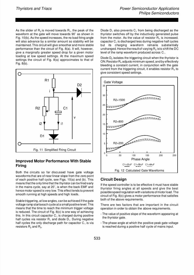
7/25/2019 Thyristors and Triacs
http://slidepdf.com/reader/full/thyristors-and-triacs 49/84
Thyristors and Triacs Power Semiconductor Applications Philips Semiconductors
As the slider of R2 is moved towards R1, the peak of thewaveform at the gate will move towards 90˚ as shown inFig. 10(b). As the speed increases, the no load firing anglewill also advance by a similar amount so stability will bemaintained.This circuit will give smoother and more stable
performance than the circuit of Fig. 8(a). It will, however,give a marginally greater speed drop for a given motorloading at low speed settings. At the maximum speedsettings the circuit of Fig. 8(a) approximates to that ofFig. 8(b).
Fig. 11 Simplified Firing Circuit
Improved Motor Performance With StableFiring
Both the circuits so far discussed have gate voltagewaveforms that are of near linear slope from the zero pointof each positive half cycle, see Figs. 10(a) and (b). Thismeans that the only timethat the thyristor can be fired earlyin the mains cycle, say at 20˚, is when the back EMF andhence motor speed is very low. This effect tends to preventsmooth running at high speeds and high loads.
Stable triggering, at low angles, can be achieved if the gatevoltage ramp startseach cycle ata smallpositive level.Thismeans that the time to reach the minimum trigger voltageis reduced. The circuit of Fig. 8(c) is one way of achievingthis. In this circuit capacitor C1 is charged during positivehalf cycles via resistor R1 and diode D1. During negativehalf cycles the only discharge path for capacitor C1 is viaresistors R2 and R3.
Diode D1 also prevents C1 from being discharged as thethyristor switches off by the inductively generated pulsefrom the motor. As the value of resistor R2 is increased,capacitor C1 is discharged less during negative half cyclesbut its charging waveform remains substantially
unchanged. Hence theresultof varying R2 isto shift the DClevel of the ramp waveform produced across C1.
Diode D2 isolates the triggering circuit when the thyristor isON.Resistor R4 adjusts minimum speed,and by effectivelybleeding a constant current, in conjunction with the gatecurrent from the triggering circuit, it enables resistor R2 togive consistent speed settings.
Fig. 12 Calculated Gate Waveforms
Circuit Design
If the speed controller is to be effective it must have stablethyristor firing angles at all speeds and give the best
possiblespeed regulation with variations ofmotor load. Thecircuit of Fig. 8(c) gives a motor performance that satisfiesboth of the above requirements.
There are two factors that are important in the circuitoperation in order to obtain the above requirements.
- The value of positive slope of the waveform appearing atthe thyristor gate.
- The phase angle at which the positive peak gate voltageis reached during a positive half cycle of mains input.
R1
R2
D2
D1
C1
v
i
i1i2
0 50 100 150 200 2500
5
10
15
20
25
30
35
Phase Angle
Gate Voltage
C1=32uF C1=50uF C1=64uF
R2=1500
R2=800
R2=200
533
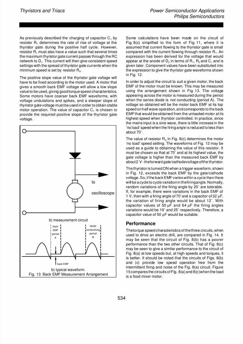
7/25/2019 Thyristors and Triacs
http://slidepdf.com/reader/full/thyristors-and-triacs 50/84
Thyristors and Triacs Power Semiconductor Applications Philips Semiconductors
As previously described the charging of capacitor C1 byresistor R1 determines the rate of rise of voltage at thethyristor gate during the positive half cycle. However,resistor R1 must also have a value such that several timesthe maximum thyristor gate current passes through the RC
network to D1. This current will then give consistent speedsettings with the spread of thyristor gate currents when theminimum speed is set by resistor R4.
The positive slope value of the thyristor gate voltage willhave to be fixed according to the motor used. A motor thatgives a smooth back EMF voltage will allow a low slopevalue to be used, giving goodtorque speedcharacteristics.Some motors have coarser back EMF waveforms, withvoltage undulations and spikes, and a steeper slope ofthyristor gate voltage must beused in order to obtain stablemotor operation. The value of capacitor C1 is chosen toprovide the required positive slope of the thyristor gate
voltage.
b) measurement circuit
b) typical waveform.Fig. 13 Back EMF Measurement Arrangement
Some calculations have been made on the circuit ofFig. 8(c) simplified to the form of Fig. 11, where it isassumed that current flowing to the thyristor gate is smallcompared with the current flowing through resistor R1. Anexpression has been derived for the voltage that would
appear at the anode of D2 in terms of R1, R2 and C1 and isgiven later. Component values have been substituted intothe expression to give the thyristor gate waveforms shownin Fig. 12.
In order to adjust the circuit to suit a given motor, the backEMF of the motor must be known. This may be measuredusing the arrangement shown in Fig. 13. The voltageappearing across the motor is measured during the periodwhen the series diode is not conducting (period A). Thevoltage so obtained will be the motor back EMF at its topspeed on half wave operation, andcorresponds to the backEMFthat would be obtained from the unloaded motor at itshighest speed when thyristor controlled. In practice, sincethe mains input is a sine wave, there is little increase in the’no load’ speed when the firingangle is reduced to less thanabout 70˚.
The value of resistor R2 in Fig. 8(c) determines the motor’no load’ speed setting. The waveforms of Fig. 12 may beused as a guide to obtaining the value of this resistor. Itmust be chosen so that at 70˚ and at its highest value, thegate voltage is higher than the measured back EMF byabout2 V - theforwardgate/cathodevoltage ofthe thyristor.
The thyristor is turnedON when a trigger waveform,shownin Fig. 12, exceeds the back EMF by the gate/cathodevoltage. So, if the back EMF varies withina cycle then there
will be a cycle to cycle variation in thefiringangle. Normally,random variations of the firing angle by 20˚ are tolerable.If, for example, there were variations in the back EMF of1 V, then with a firing angle of 70˚and a capacitor of 32 µF,the variation of firing angle would be about 12˚. Withcapacitor values of 50 µF and 64 µF the firing anglesvariations would be 19˚ and 25˚ respectively. Therefore, acapacitor value of 50 µF would be suitable.
Performance
Thetorque speed characteristics of thethree circuits,whenused to drive an electric drill, are compared in Fig. 14. It
may be seen that the circuit of Fig. 8(b) has a poorerperformance than the two other circuits. That of Fig. 8(c)may be seen to give a similar performance to the circuit ofFig. 8(a) at low speeds but, at high speeds and torques, itis better. It should be noted that the circuits of Figs. 8(b)and (c) provide low speed operation free from theintermittent firing and noise of the Fig. 8(a) circuit. Figure15compares the circuits of Fig. 8(a)and 8(c)when the loadis a food mixer motor.
to
oscilloscope
back
EMF
period
diode
conductiong
period
BA
back EMF
534
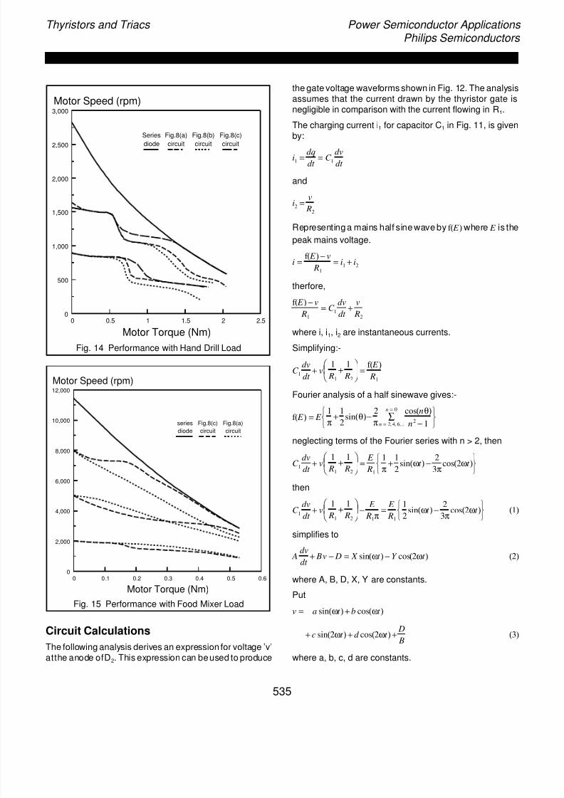
7/25/2019 Thyristors and Triacs
http://slidepdf.com/reader/full/thyristors-and-triacs 51/84
Thyristors and Triacs Power Semiconductor Applications Philips Semiconductors
Fig. 14 Performance with Hand Drill Load
Fig. 15 Performance with Food Mixer Load
Circuit Calculations
The following analysis derives an expression for voltage ’v’atthe anode ofD2. This expression can beused to produce
the gate voltage waveforms shown in Fig. 12. The analysisassumes that the current drawn by the thyristor gate isnegligible in comparison with the current flowing in R1.
The charging current i1 for capacitor C1 in Fig. 11, is given
by:
and
Representing a mains half sine wave by where is the
peak mains voltage.
therfore,
where i, i1, i2 are instantaneous currents.
Simplifying:-
Fourier analysis of a half sinewave gives:-
neglecting terms of the Fourier series with n > 2, then
then
simplifies to
where A, B, D, X, Y are constants.
Put
where a, b, c, d are constants.
0 0.5 1 1.5 2 2.50
500
1,000
1,500
2,000
2,500
3,000
Motor Torque (Nm)
Motor Speed (rpm)
Series
diode
Fig.8(a)
circuit
Fig.8(b)
circuit
Fig.8(c)
circuit
i1 = dq
dt = C 1
dv
dt
i2 = v
R2
f ( E ) E
i = f ( E ) − v
R1
= i1 + i2
f ( E ) − v
R1
= C 1dv
dt +
v
R2
C 1dv
dt + v
1
R1
+ 1
R2
=
f ( E ) R1
0 0.1 0.2 0.3 0.4 0.5 0.60
2,000
4,000
6,000
8,000
10,000
12,000
Motor Torque (Nm)
Motor Speed (rpm)
series
diode
Fig.8(c)
circuit
Fig.8(a)
circuit
f ( E ) = E
1
π +
1
2sin(θ)−
2
π ∑n = 2, 4, 6...
n = 0 cos(nθ)n2 − 1
C 1dv
dt + v
1
R1
+ 1
R2
=
E
R1
1
π+
1
2sin(ωt ) −
2
3πcos(2ωt )
C 1dv
dt + v
1
R1
+ 1
R2
−
E
R1π =
E
R1
1
2sin(ωt ) −
2
3πcos(2ωt )
(1)
A
dv
dt + Bv − D = X sin(ωt ) − Y cos(2ωt ) (2)
v = a sin(ωt ) + b cos(ωt )
+ c sin(2ωt ) + d cos(2ωt ) + D
B (3)
535
7/25/2019 Thyristors and Triacs
http://slidepdf.com/reader/full/thyristors-and-triacs 52/84
Thyristors and Triacs Power Semiconductor Applications Philips Semiconductors
substituting (3) and (4) in equation (2) and equating termsin , then
substituting for the constants in equation (2) gives:
This may be simplified since
Sothe voltage that the trigger circuit would apply tothe gate(assuming the gate draws no current) is given by:
Solving this equation for a different values of C1 andpositions of R2 gives the curves shown in Fig. 12.
Conclusions
The addition of electronic control can enhance the overalluseability of many domestic products. Cost andperformance requirements are major factors whendetermining the type of control circuit to be used in theseapplications. It is possible, using thyristors and triacs, toconstruct a range of phase control circuits which can meetmany of these cost and operational requirements.
Althoughthesecircuitsarenot complex anduse only simplecomponents,it isstill importantto designwith care toensurethat thebestperformanceis achieved.This reporthas givenexamples of some of these circuits and has highlighted theareas of their design requiring particular care.
dv
dt = aωcos(ωt ) − bωsin(ωt )
+ 2cωcos(2ωt ) − 2d ωsin(2ωt ) (4)
v = R2 E
π( R1 + R2)
+ R2 E
2ω2C 1
2 R1
2 R2
2( R1 + R2)sin(ωt )
− ωC 1 R1 R2 cos(ωt )
− 2
3πωC 1 R1 R2 sin(2ωt )
− 1
3π( R1 + R2)cos(2ωt )
cos(ωt ),cos(2ωt ),sin(ωt ),sin(2ωt )
v = BX
A2ω2 + B2.sin(ωt ) −
Aω X
A2ω2 + B2.cos(ωt )
− 2 AωY
4 A2ω2 + B2.sin(2ωt )
− BY
4 A2ω2 + B2.cos(2ωt ) +
D
B
v = R2
E .( R1 + R2)sin(ωt ) − ωC 1 R1 R2 cos(ωt )
2ω2C 12 R12 R22 + ( R1 + R2)2
+ R2 E . 1
π( R1 + R2)
− R2 E .4ωC 1 R1 R2 sin(2ωt ) + 4( R1 + R2)cos(2ωt )
3π[4ω2C 12 R1
2 R22 + ( R1 + R2)2]
( R1 + R2)2
2ω2C
2 R1
2 R2
2
536
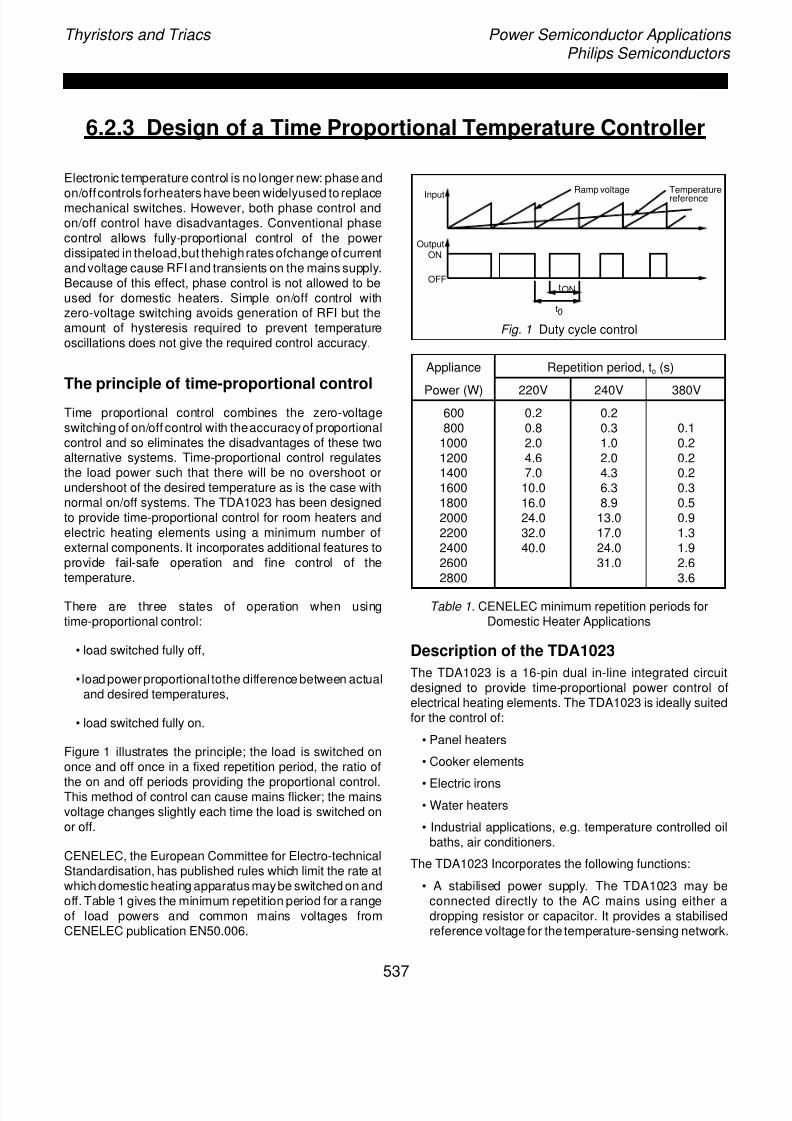
7/25/2019 Thyristors and Triacs
http://slidepdf.com/reader/full/thyristors-and-triacs 53/84
Thyristors and Triacs Power Semiconductor Applications Philips Semiconductors
6.2.3 Design of a Time Proportional Temperature Controller
Electronic temperature control is no longer new: phase and
on/offcontrols forheaters have been widelyused to replacemechanical switches. However, both phase control andon/off control have disadvantages. Conventional phasecontrol allows fully-proportional control of the powerdissipated in theload,but thehighrates ofchange ofcurrentand voltage cause RFI and transients on the mains supply.Because of this effect, phase control is not allowed to beused for domestic heaters. Simple on/off control withzero-voltage switching avoids generation of RFI but theamount of hysteresis required to prevent temperatureoscillations does not give the required control accuracy.
The principle of time-proportional control
Time proportional control combines the zero-voltageswitching of on/off control with the accuracyof proportionalcontrol and so eliminates the disadvantages of these twoalternative systems. Time-proportional control regulatesthe load power such that there will be no overshoot orundershoot of the desired temperature as is the case withnormal on/off systems. The TDA1023 has been designedto provide time-proportional control for room heaters andelectric heating elements using a minimum number ofexternal components. It incorporates additional features toprovide fail-safe operation and fine control of thetemperature.
There are three states of operation when usingtime-proportional control:
• load switched fully off,
• load powerproportional tothe difference between actualand desired temperatures,
• load switched fully on.
Figure 1 illustrates the principle; the load is switched ononce and off once in a fixed repetition period, the ratio of
the on and off periods providing the proportional control.This method of control can cause mains flicker; the mainsvoltage changes slightly each time the load is switched onor off.
CENELEC, the European Committee for Electro-technicalStandardisation, has published rules which limit the rate atwhich domestic heating apparatus maybe switched on andoff. Table 1 gives the minimum repetition period for a rangeof load powers and common mains voltages fromCENELEC publication EN50.006.
Fig. 1 Duty cycle control
Appliance Repetition period, to (s)
Power (W) 220V 240V 380V600 0.2 0.2800 0.8 0.3 0.1
1000 2.0 1.0 0.21200 4.6 2.0 0.21400 7.0 4.3 0.21600 10.0 6.3 0.31800 16.0 8.9 0.52000 24.0 13.0 0.92200 32.0 17.0 1.32400 40.0 24.0 1.92600 31.0 2.62800 3.6
Table 1. CENELEC minimum repetition periods forDomestic Heater Applications
Description of the TDA1023
The TDA1023 is a 16-pin dual in-line integrated circuitdesigned to provide time-proportional power control ofelectrical heating elements. The TDA1023 is ideally suitedfor the control of:
• Panel heaters
• Cooker elements
• Electric irons• Water heaters
• Industrial applications, e.g. temperature controlled oilbaths, air conditioners.
The TDA1023 Incorporates the following functions:
• A stabilised power supply. The TDA1023 may beconnected directly to the AC mains using either adropping resistor or capacitor. It provides a stabilisedreference voltage for the temperature-sensing network.
ON
OFF
Input
Output
t0
tON
Temperaturereference
Ramp voltage
537
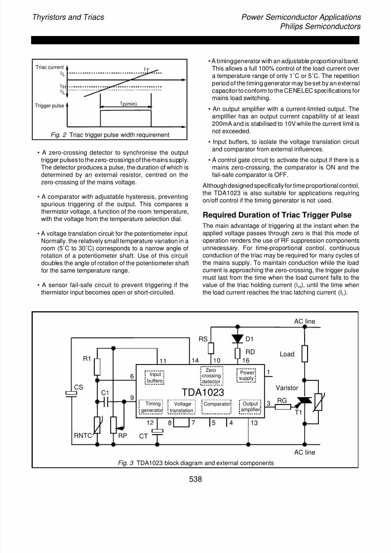
7/25/2019 Thyristors and Triacs
http://slidepdf.com/reader/full/thyristors-and-triacs 54/84
Thyristors and Triacs Power Semiconductor Applications Philips Semiconductors
Fig. 2 Triac trigger pulse width requirement
• A zero-crossing detector to synchronise the outputtrigger pulsesto thezero-crossingsof themains supply.The detector produces a pulse, the duration of which isdetermined by an external resistor, centred on thezero-crossing of the mains voltage.
• A comparator with adjustable hysteresis, preventingspurious triggering of the output. This compares athermistor voltage, a function of the room temperature,with the voltage from the temperature selection dial.
• A voltage translation circuit for the potentiometer input.Normally, the relatively small temperature variation in aroom (5˚C to 30˚C) corresponds to a narrow angle ofrotation of a potentiometer shaft. Use of this circuitdoubles the angle of rotation of the potentiometer shaftfor the same temperature range.
• A sensor fail-safe circuit to prevent triggering if the
thermistor input becomes open or short-circuited.
• A timinggenerator with an adjustable proportionalband.This allows a full 100% control of the load current overa temperature range of only 1˚C or 5˚C. The repetitionperiod of the timing generator may beset by an externalcapacitor to conform to the CENELEC specifications for
mains load switching.
• An output amplifier with a current-limited output. Theamplifier has an output current capability of at least200mA and is stabilised to 10V while the current limit isnot exceeded.
• Input buffers, to isolate the voltage translation circuitand comparator from external influences.
• A control gate circuit to activate the output if there is amains zero-crossing, the comparator is ON and thefail-safe comparator is OFF.
Althoughdesigned specifically for timeproportional control,
the TDA1023 is also suitable for applications requiringon/off control if the timing generator is not used.
Required Duration of Triac Trigger Pulse
The main advantage of triggering at the instant when theapplied voltage passes through zero is that this mode ofoperation renders the use of RF suppression componentsunnecessary. For time-proportional control, continuousconduction of the triac may be required for many cycles ofthe mains supply. To maintain conduction while the loadcurrent is approaching the zero-crossing, the trigger pulsemust last from the time when the load current falls to thevalue of the triac holding current (IH), until the time when
the load current reaches the triac latching current (IL).
I L
IHIL
tp(min)
ITTriac current
Trigger pulse
Fig. 3 TDA1023 block diagram and external components
1
3
13457812
9
6
11 14 10 16
AC line
AC line
D1
RD
RS
R1
RP
CS
RNTC
Load
RG
CT
C1 Varistor
Input
buffers
Timing
generator
Voltage
translation
Zerocrossingdetector
Powersupply
Outputamplifier
Comparator
TDA1023
T1
538
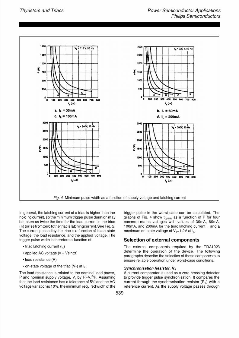
7/25/2019 Thyristors and Triacs
http://slidepdf.com/reader/full/thyristors-and-triacs 55/84
Thyristors and Triacs Power Semiconductor Applications Philips Semiconductors
Fig. 4 Minimum pulse width as a function of supply voltage and latching current
In general, the latching current of a triac is higher than theholding current, so the minimum trigger pulse duration maybe taken as twice the time for the load current in the triac(IT) torise fromzero tothe triac’s latchingcurrent.See Fig. 2.The current passed by the triac is a function of its on-state
voltage, the load resistance, and the applied voltage. Thetrigger pulse width is therefore a function of:
• triac latching current (IL)
• applied AC voltage (v = Vsinωt)
• load resistance (R)
• on-state voltage of the triac (VT) at IL.
The load resistance is related to the nominal load power,P and nominal supply voltage, Vs by R=Vs
2 /P. Assumingthat the load resistance has a tolerance of 5% and the ACvoltage variation is 10%, theminimum required width of the
trigger pulse in the worst case can be calculated. Thegraphs of Fig. 4 show tp(MIN) as a function of P for fourcommon mains voltages with values of 30mA, 60mA,100mA, and 200mA for the triac latching current IL and amaximum on-state voltage of VT=1.2V at IL.
Selection of external components
The external components required by the TDA1023determine the operation of the device. The followingparagraphs describe the selection of these components toensure reliable operation under worst-case conditions.
Synchronisation Resistor, R S
A current comparator is used as a zero-crossing detectorto provide trigger pulse synchronisation. It compares thecurrent through the synchronisation resistor (RS) with areference current. As the supply voltage passes through
539
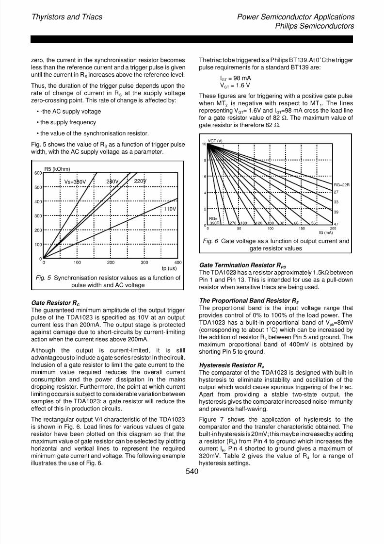
7/25/2019 Thyristors and Triacs
http://slidepdf.com/reader/full/thyristors-and-triacs 56/84
Thyristors and Triacs Power Semiconductor Applications Philips Semiconductors
zero, the current in the synchronisation resistor becomesless than the reference current and a trigger pulse is givenuntil the current in RS increases above the reference level.
Thus, the duration of the trigger pulse depends upon the
rate of change of current in RS at the supply voltagezero-crossing point. This rate of change is affected by:
• -the AC supply voltage
• the supply frequency
• the value of the synchronisation resistor.
Fig. 5 shows the value of RS as a function of trigger pulsewidth, with the AC supply voltage as a parameter.
Fig. 5 Synchronisation resistor values as a function of
pulse width and AC voltage
Gate Resistor R G
The guaranteed minimum amplitude of the output triggerpulse of the TDA1023 is specified as 10V at an outputcurrent less than 200mA. The output stage is protectedagainst damage due to short-circuits by current-limitingaction when the current rises above 200mA.
Although the output is current-limited, it is stilladvantageousto include a gate series resistor in thecircuit.Inclusion of a gate resistor to limit the gate current to theminimum value required reduces the overall current
consumption and the power dissipation in the mainsdropping resistor. Furthermore, the point at which currentlimiting occurs is subject to considerable variationbetweensamples of the TDA1023: a gate resistor will reduce theeffect of this in production circuits.
The rectangular output V/I characteristic of the TDA1023is shown in Fig. 6. Load lines for various values of gateresistor have been plotted on this diagram so that themaximum value of gate resistor can be selected by plottinghorizontal and vertical lines to represent the requiredminimum gate current and voltage. The following exampleillustrates the use of Fig. 6.
Thetriac tobe triggeredis a Philips BT139.At 0˚Cthe triggerpulse requirements for a standard BT139 are:
IGT = 98 mAVGT = 1.6 V
These figures are for triggering with a positive gate pulsewhen MT2 is negative with respect to MT1. The linesrepresenting VGT= 1.6V and IGT=98 mA cross the load linefor a gate resistor value of 82 Ω. The maximum value ofgate resistor is therefore 82 Ω.
Fig. 6 Gate voltage as a function of output current andgate resistor values
Gate Termination Resistor R PD
TheTDA1023 has a resistor approximately 1.5kΩ betweenPin 1 and Pin 13. This is intended for use as a pull-down
resistor when sensitive triacs are being used.
The Proportional Band Resistor R 5
The proportional band is the input voltage range thatprovides control of 0% to 100% of the load power. TheTDA1023 has a built-in proportional band of Vpb=80mV(corresponding to about 1˚C) which can be increased bythe addition of resistor R5 between Pin 5 and ground. Themaximum proportional band of 400mV is obtained byshorting Pin 5 to ground.
Hysteresis Resistor R 4
The comparator of the TDA1023 is designed with built-in
hysteresis to eliminate instability and oscillation of theoutput which would cause spurious triggering of the triac.Apart from providing a stable two-state output, thehysteresis gives the comparator increased noise immunityand prevents half-waving.
Figure 7 shows the application of hysteresis to thecomparator and the transfer characteristic obtained. Thebuilt-inhysteresis is20mV; this maybe increasedby addinga resistor (R4) from Pin 4 to ground which increases thecurrent IH. Pin 4 shorted to ground gives a maximum of320mV. Table 2 gives the value of R4 for a range ofhysteresis settings.
0 50 100 150 2000
2
4
6
8
10
RG=22R
27
33
39
47566882100120180270RG=390R
IG (mA)
VGT (V)
0 100 200 300 4000
100
200
300
400
500
600
Vs=380V 240V 220V
110V
tp (us)
R5 (kOhm)
540
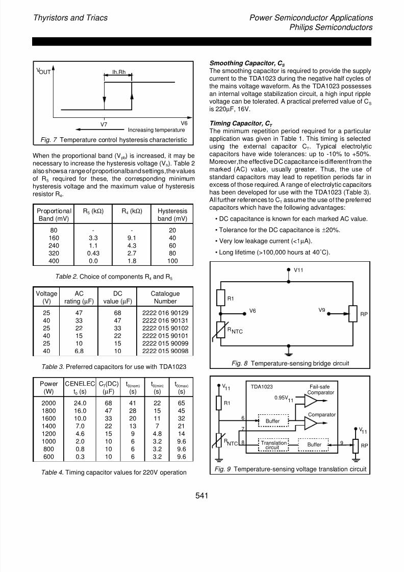
7/25/2019 Thyristors and Triacs
http://slidepdf.com/reader/full/thyristors-and-triacs 57/84
Thyristors and Triacs Power Semiconductor Applications Philips Semiconductors
Fig. 7 Temperature control hysteresis characteristic
When the proportional band (Vpb) is increased, it may benecessary to increase the hysteresis voltage (Vh). Table 2also showsa rangeofproportionalbandsettings,thevaluesof R5 required for these, the corresponding minimumhysteresis voltage and the maximum value of hysteresisresistor R4.
Proportional R5 (kΩ) R4 (kΩ) HysteresisBand (mV) band (mV)
80 - - 20160 3.3 9.1 40240 1.1 4.3 60320 0.43 2.7 80400 0.0 1.8 100
Table 2 . Choice of components R4 and R5
Voltage AC DC Catalogue
(V) rating (µF) value (µF) Number
25 47 68 2222 016 9012940 33 47 2222 016 9013125 22 33 2222 015 9010240 15 22 2222 015 9010125 10 15 2222 015 9009940 6.8 10 2222 015 90098
Table 3 . Preferred capacitors for use with TDA1023
Power CENELEC CT(DC) t0(nom) t0(min) t0(max)
(W) t0 (s) (µF) (s) (s) (s)
2000 24.0 68 41 22 651800 16.0 47 28 15 451600 10.0 33 20 11 321400 7.0 22 13 7 211200 4.6 15 9 4.8 141000 2.0 10 6 3.2 9.6800 0.8 10 6 3.2 9.6600 0.3 10 6 3.2 9.6
Table 4 . Timing capacitor values for 220V operation
Smoothing Capacitor, C S
The smoothing capacitor is required to provide the supplycurrent to the TDA1023 during the negative half cycles ofthe mains voltage waveform. As the TDA1023 possessesan internal voltage stabilization circuit, a high input ripple
voltage can be tolerated. A practical preferred value of CS
is 220µF, 16V.
Timing Capacitor, C T
The minimum repetition period required for a particularapplication was given in Table 1. This timing is selectedusing the external capacitor CT. Typical electrolyticcapacitors have wide tolerances: up to -10% to +50%.Moreover,the effectiveDC capacitance is different from themarked (AC) value, usually greater. Thus, the use ofstandard capacitors may lead to repetition periods far inexcess of those required. A range of electrolytic capacitorshas been developed for use with the TDA1023 (Table 3).
All further references to CT assume the use of the preferredcapacitors which have the following advantages:
• DC capacitance is known for each marked AC value.
• Tolerance for the DC capacitance is ±20%.
• Very low leakage current (<1µA).
• Long lifetime (>100,000 hours at 40˚C).
Fig. 8 Temperature-sensing bridge circuit
Fig. 9 Temperature-sensing voltage translation circuit
V7 V6Increasing temperature
VOUT Ih.Rh
V9V6
R1
RNTC
RP
V11
BufferTranslationcircuit
Buffer
Comparator
Fail-safeComparator
0.95V11
6
7
8 9
TDA1023
V11
RPR
V11
R1
NTC
541
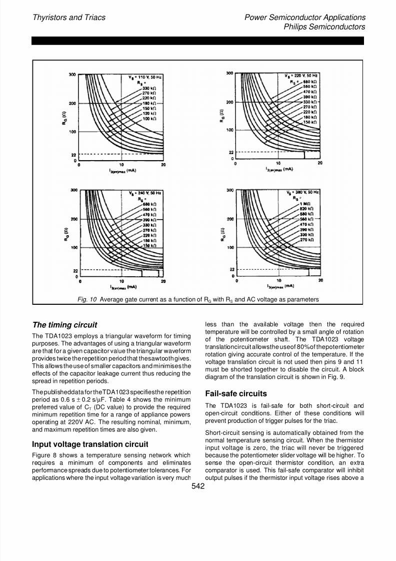
7/25/2019 Thyristors and Triacs
http://slidepdf.com/reader/full/thyristors-and-triacs 58/84
Thyristors and Triacs Power Semiconductor Applications Philips Semiconductors
Fig. 10 Average gate current as a function of RG with RS and AC voltage as parameters
The timing circuit
The TDA1023 employs a triangular waveform for timingpurposes. The advantages of using a triangular waveformare that for a given capacitor value the triangular waveformprovides twice therepetition period that thesawtoothgives.This allows theuseof smaller capacitors andminimisestheeffects of the capacitor leakage current thus reducing thespread in repetition periods.
Thepublisheddata for theTDA1023specifiesthe repetitionperiod as 0.6 s ± 0.2 s/ µF. Table 4 shows the minimumpreferred value of CT (DC value) to provide the requiredminimum repetition time for a range of appliance powersoperating at 220V AC. The resulting nominal, minimum,and maximum repetition times are also given.
Input voltage translation circuit
Figure 8 shows a temperature sensing network whichrequires a minimum of components and eliminatesperformance spreads due to potentiometer tolerances. Forapplications where the input voltage variation is very much
less than the available voltage then the requiredtemperature will be controlled by a small angle of rotationof the potentiometer shaft. The TDA1023 voltagetranslationcircuitallowstheuseof 80%of thepotentiometerrotation giving accurate control of the temperature. If thevoltage translation circuit is not used then pins 9 and 11must be shorted together to disable the circuit. A blockdiagram of the translation circuit is shown in Fig. 9.
Fail-safe circuitsThe TDA1023 is fail-safe for both short-circuit andopen-circuit conditions. Either of these conditions willprevent production of trigger pulses for the triac.
Short-circuit sensing is automatically obtained from thenormal temperature sensing circuit. When the thermistorinput voltage is zero, the triac will never be triggeredbecause the potentiometer slider voltage will be higher. Tosense the open-circuit thermistor condition, an extracomparator is used. This fail-safe comparator will inhibitoutput pulses if the thermistor input voltage rises above a
542
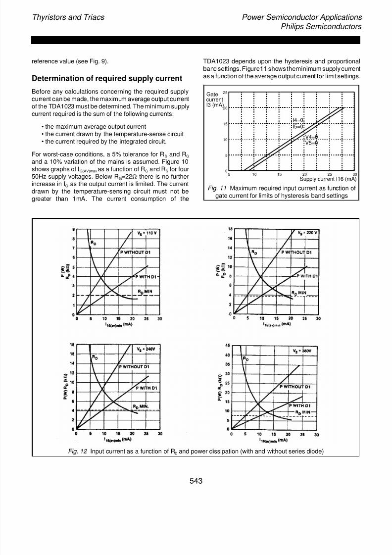
7/25/2019 Thyristors and Triacs
http://slidepdf.com/reader/full/thyristors-and-triacs 59/84
Thyristors and Triacs Power Semiconductor Applications Philips Semiconductors
reference value (see Fig. 9).
Determination of required supply current
Before any calculations concerning the required supply
current can be made, the maximum average output currentof the TDA1023 must be determined. The minimum supplycurrent required is the sum of the following currents:
• the maximum average output current• the current drawn by the temperature-sense circuit• the current required by the integrated circuit.
For worst-case conditions, a 5% tolerance for RS and RG
and a 10% variation of the mains is assumed. Figure 10shows graphs of IG(AV)max as a function of RG and RS for four50Hz supply voltages. Below RG=22Ω there is no furtherincrease in IG as the output current is limited. The current
drawn by the temperature-sensing circuit must not begreater than 1mA. The current consumption of the
TDA1023 depends upon the hysteresis and proportionalband settings.Figure11 showstheminimum supplycurrentas a function of the average outputcurrent for limit settings.
Fig. 11 Maximum required input current as function of
gate current for limits of hysteresis band settings
5 10 15 20 25 300
5
10
15
20
25
GatecurrentI3 (mA)
Supply current I16 (mA)
I4=0I5=0
V4=0V5=0
Fig. 12 Input current as a function of RD and power dissipation (with and without series diode)
543
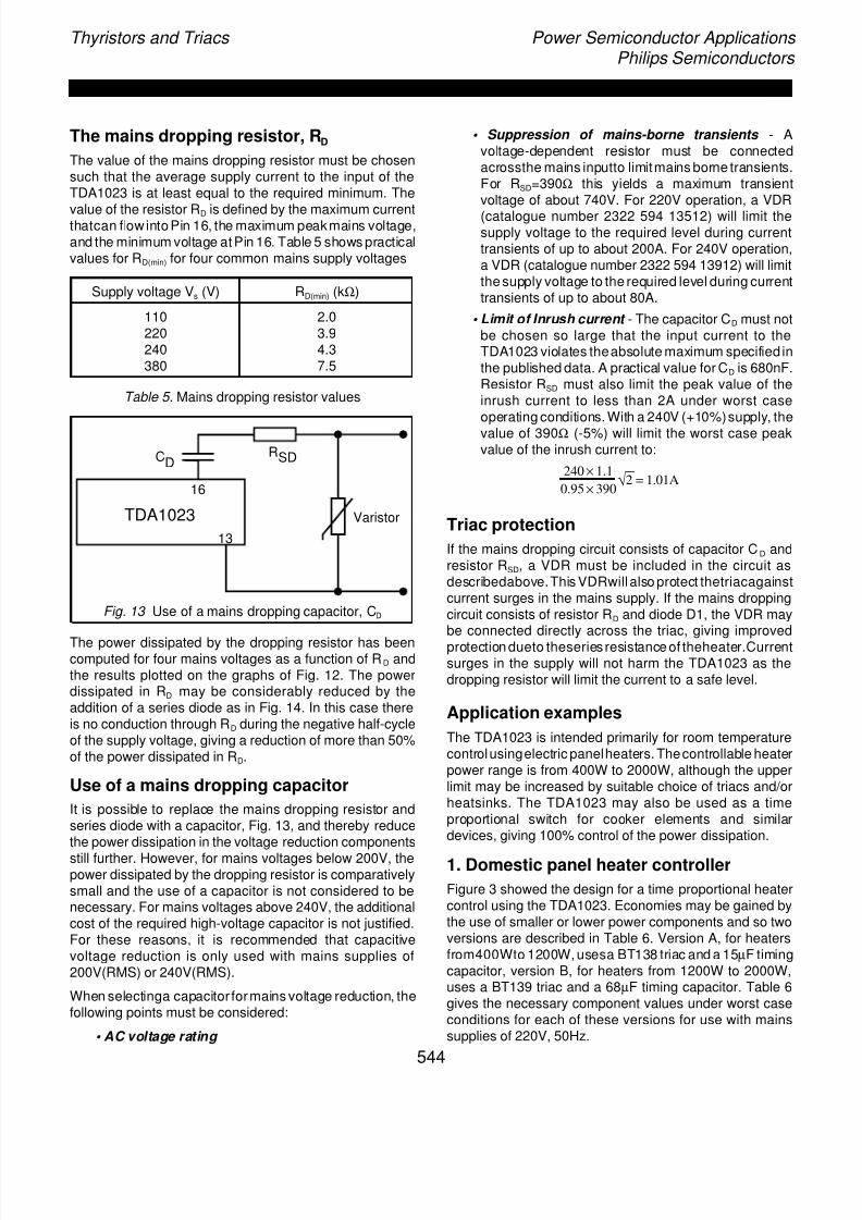
7/25/2019 Thyristors and Triacs
http://slidepdf.com/reader/full/thyristors-and-triacs 60/84
Thyristors and Triacs Power Semiconductor Applications Philips Semiconductors
The mains dropping resistor, RD
The value of the mains dropping resistor must be chosensuch that the average supply current to the input of theTDA1023 is at least equal to the required minimum. The
value of the resistor RD is defined by the maximum currentthatcan flow into Pin 16, the maximum peakmains voltage,and the minimum voltage at Pin 16. Table 5 shows practicalvalues for RD(min) for four common mains supply voltages
Supply voltage Vs (V) RD(min) (kΩ)
110 2.0220 3.9240 4.3380 7.5
Table 5 . Mains dropping resistor values
Fig. 13 Use of a mains dropping capacitor, CD
The power dissipated by the dropping resistor has beencomputed for four mains voltages as a function of RD andthe results plotted on the graphs of Fig. 12. The powerdissipated in RD may be considerably reduced by theaddition of a series diode as in Fig. 14. In this case thereis no conduction through RD during the negative half-cycleof the supply voltage, giving a reduction of more than 50%of the power dissipated in RD.
Use of a mains dropping capacitor
It is possible to replace the mains dropping resistor andseries diode with a capacitor, Fig. 13, and thereby reducethe power dissipation in the voltage reduction components
still further. However, for mains voltages below 200V, thepower dissipated by the dropping resistor is comparativelysmall and the use of a capacitor is not considered to benecessary. For mains voltages above 240V, the additionalcost of the required high-voltage capacitor is not justified.For these reasons, it is recommended that capacitivevoltage reduction is only used with mains supplies of200V(RMS) or 240V(RMS).
When selectinga capacitor formains voltage reduction, thefollowing points must be considered:
• AC voltage rating
• Suppression of mains-borne transients - Avoltage-dependent resistor must be connectedacrossthe mains inputto limitmains borne transients.For RSD=390Ω this yields a maximum transientvoltage of about 740V. For 220V operation, a VDR
(catalogue number 2322 594 13512) will limit thesupply voltage to the required level during currenttransients of up to about 200A. For 240V operation,a VDR (catalogue number 2322 594 13912) will limitthe supply voltage to the required level during currenttransients of up to about 80A.
• Limit of Inrush current - The capacitor CD must notbe chosen so large that the input current to theTDA1023 violates theabsolute maximum specified inthe published data. A practical value for CD is 680nF.Resistor RSD must also limit the peak value of theinrush current to less than 2A under worst caseoperating conditions. With a 240V (+10%)supply, thevalue of 390Ω (-5%) will limit the worst case peakvalue of the inrush current to:
Triac protection
If the mains dropping circuit consists of capacitor CD andresistor RSD, a VDR must be included in the circuit asdescribedabove.This VDRwill also protect thetriacagainstcurrent surges in the mains supply. If the mains droppingcircuit consists of resistor RD and diode D1, the VDR maybe connected directly across the triac, giving improvedprotection dueto theseries resistance of theheater.Currentsurges in the supply will not harm the TDA1023 as thedropping resistor will limit the current to a safe level.
Application examples
The TDA1023 is intended primarily for room temperaturecontrolusingelectric panelheaters. Thecontrollable heaterpower range is from 400W to 2000W, although the upperlimit may be increased by suitable choice of triacs and/orheatsinks. The TDA1023 may also be used as a timeproportional switch for cooker elements and similardevices, giving 100% control of the power dissipation.
1. Domestic panel heater controller
Figure 3 showed the design for a time proportional heatercontrol using the TDA1023. Economies may be gained bythe use of smaller or lower power components and so twoversions are described in Table 6. Version A, for heatersfrom400Wto 1200W, usesa BT138 triac and a 15µF timingcapacitor, version B, for heaters from 1200W to 2000W,uses a BT139 triac and a 68µF timing capacitor. Table 6gives the necessary component values under worst caseconditions for each of these versions for use with mainssupplies of 220V, 50Hz.
13
16
CDRSD
VaristorTDA1023
240 × 1.1
0.95 × 390√ 2 = 1.01A
544

7/25/2019 Thyristors and Triacs
http://slidepdf.com/reader/full/thyristors-and-triacs 61/84
Thyristors and Triacs Power Semiconductor Applications Philips Semiconductors
The capacitor C1 has been included in the circuit of Fig. 3to minimise sensor line interference pick-up. This is onlynecessary when the sensor is remote from the controlcircuit. The built-in hysteresis and proportional bandprovides optimum performance for panel heaters so pins 4
and 5 are not connected.
Component Version A Version B400W - 1200W 1200W - 2000W
T1 BT138-500 BT139-500VDR 1 350V, 1mA 350V, 1mA
D1 BYX10G BYX10GR1
2 18.7kΩ 18.7kΩRNTC 3 R25=22kΩ,B=4200k R25=22kΩ, B=4200k
RP 22kΩ 22kΩRD 4.3kΩ 6.2kΩRG 82Ω 82ΩRS 430kΩ 180kΩC1 47nF 47nFCS 220µF, 16V 220µF, 16VCT 15µF (DC) 68µF (DC)
CD 4 680nF 470nFRSD 4 390Ω 390Ω
Notes: 1. Cat. No. 2322 594 135122. 1% tolerance3. Cat. No. 2322 642 122234. Only required if used in place of D1 and RD
Table 6 . 220V, 50Hz temperature controller components
2. Temperature control of 2kW load.
For a loadpowerof 2kW the BT139 triac must beused.Thecircuit is also that shown in Fig. 3. Table 7 gives a summaryof the required component values.
Component Value Remarks
T1 BT139-500VDR 350V, 1mA No. 2322 594 13912D1 BYX10G
R1 18.7kΩ 1% toleranceRNTC R25=22kΩ, B=4200k No. 2322 642 12223RP 22kΩRD 6.8kΩRG 82ΩRS 150kΩC1 47nFCS 220µF, 16VCT 47µF (DC) No. 2222 016 90129
Table 7 . 2000W, 220V, 50Hz temperature controller
Value of R S
The required trigger pulse width can be found from Fig. 4as a function of the load power, latch current and supplyvoltage (2000W, 60mA, and 220V, 50Hz, respectively):tp(min)=64µs. A value of RS=135kΩ provides a trigger pulse
of the required duration. The next preferred value abovethis is 150kΩ, providing a tp(min) of approximately 70µs.
Value of R G
The maximum value of RG that may be used is determinedby the minimum conditions to reliably trigger all samples ofthe triac. In Fig. 6 it can be seen that the operation point of1.6V and 98 mA lies on the load line for 82Ω and this is thevalue chosen.
Value of C T
For a load of 2kW, the repetition period must be at least24s (from Table 1). From Table 4 the minimum preferredvalue of CT to provide this period is 68µF. However, due to
the different performance under AC and DC conditions,then from Table 3, the actual capacitor used should be47µF, 25V.
Value of R 1 and R P
For control over the range 5˚C to 35˚C and a thermistorcharacteristics with R25=22kΩ, a suitable value of R1 is18.7kΩ ±1%. A suitable value for RP is 22kΩ.
Value of R D
First, the maximum average output current must be found.From Fig. 10 the maximum gate current IG is given as afunction of the values of resistors RS and RG. For this circuitIG(AV)max=5 mA. Once the maximum average output current
is known, the minimum required supply current can befound from Fig. 11. With minimum hysteresis andproportional band, the average value of the supply currentis 12.5 mA. Using this value of input current the requiredvalue of RD can be found from Fig. 12 giving RD = 5.6 kΩ.The power dissipation in the resistor when diode D1 ispresent in the circuit is then 5 W.
3. Time proportional power control
The TDA1023 may be used to provide proportional controlof devices such as electric cooker elements. Thetemperature-sensingbridge is replaced by a potentiometer,the power in the load being proportional to the
potentiometer setting. Proportional power control is thusobtained while the potentiometer voltage lies between theupper and lower limits of the triangular waveformcomparator input.
As the timing capacitor is charged and discharged bycurrent sources, the voltage across it will never reach zero,so that load power will be zero before the potentiometerreaches its minimum setting. Similarly, maximum loadpower is reached before the maximum setting of thepotentiometer. This effect can be reduced by the additionof resistors R1 and R2. To ensure that 0% and 100% load
545

7/25/2019 Thyristors and Triacs
http://slidepdf.com/reader/full/thyristors-and-triacs 62/84
Thyristors and Triacs Power Semiconductor Applications Philips Semiconductors
power can be selected by the potentiometer setting, thevalues of R1 and R2 should each be limited to 10% of thevalue of RP.
All the circuit components are calculated in the same way
as for the temperature controller, including the timingcapacitor CT. An example circuit, with components suitablefor the control of loads from 1kW to 2kW from 220V, 50Hzsupplies, is shown in Fig. 14 and Table 8.
Component Value
T1 BT139-500VDR ZnO, 350V, 1mAD1 BYX10GR1 4.7kΩR2 4.7kΩRP 47kΩRD 5.6kΩRG 82ΩRS 220kΩCS 220µF, 16VCT 47µF, 25V
Table 8 . Time proportional power controller
Fig. 14 Time-proportional power regulation circuit
4. Phase control circuit using the TDA1023
Figure 15 shows an adjustable phase control trigger circuitsuitable for thyristor or triac controller applications. Thecircuit uses the TDA1023 control chip and an NE555 timerdeviceto give output phase control proportional to the inputvoltage command.
AC line
AC line
D1
RD
RS
CS
Load
RG
CT
VaristorTDA1023
R1
R2
RP
11 14 10 16
3
1312
7
6
9
T1
Fig. 15 Adjustable phase SCR/Triac trigger circuit
546

7/25/2019 Thyristors and Triacs
http://slidepdf.com/reader/full/thyristors-and-triacs 63/84
Thyristors and Triacs Power Semiconductor Applications Philips Semiconductors
Hi-Com Triacs
547

7/25/2019 Thyristors and Triacs
http://slidepdf.com/reader/full/thyristors-and-triacs 64/84
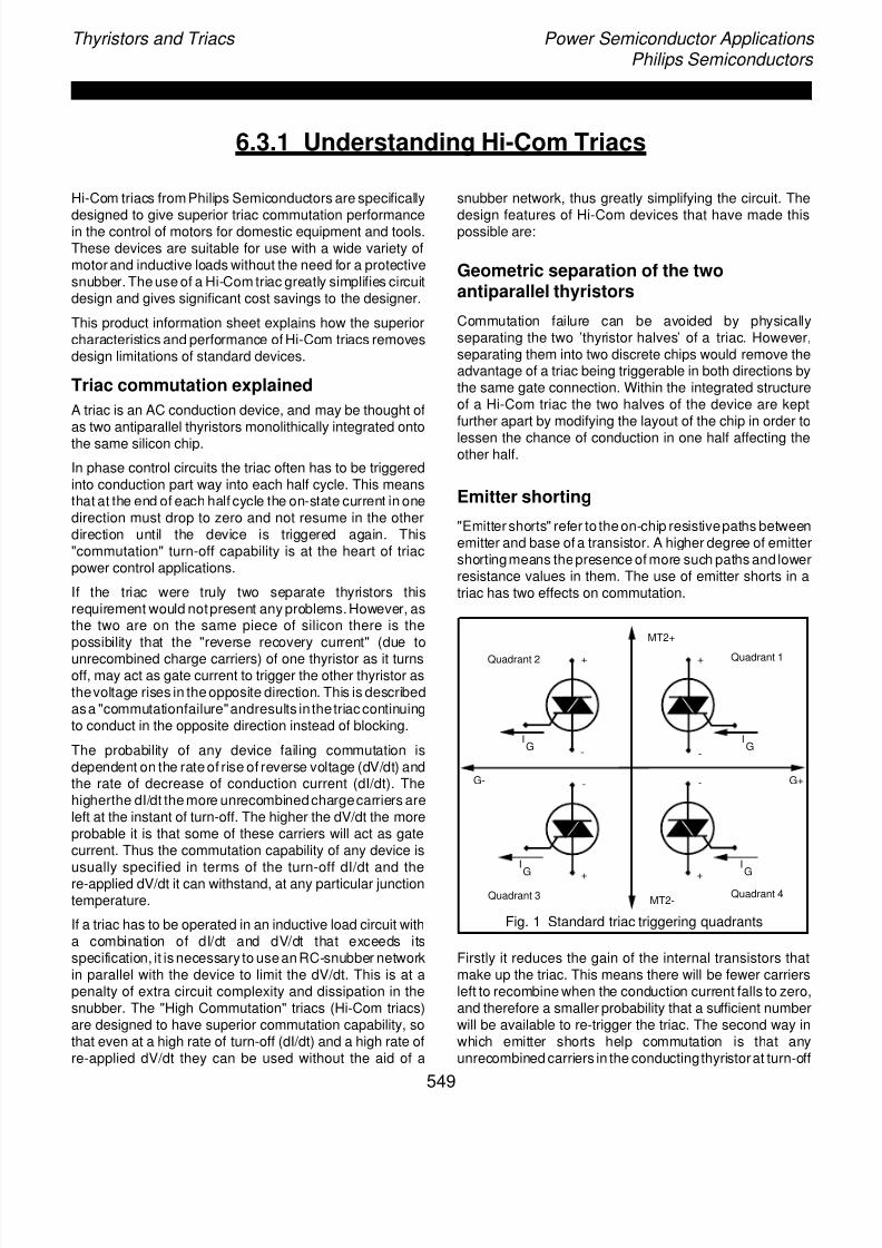
7/25/2019 Thyristors and Triacs
http://slidepdf.com/reader/full/thyristors-and-triacs 65/84
Thyristors and Triacs Power Semiconductor Applications Philips Semiconductors
6.3.1 Understanding Hi-Com Triacs
Hi-Com triacs from Philips Semiconductors are specifically
designed to give superior triac commutation performancein the control of motors for domestic equipment and tools.These devices are suitable for use with a wide variety ofmotor and inductive loads without the need for a protectivesnubber. The use of a Hi-Com triac greatly simplifies circuitdesign and gives significant cost savings to the designer.
This product information sheet explains how the superiorcharacteristics and performance of Hi-Com triacs removesdesign limitations of standard devices.
Triac commutation explained
A triac is an AC conduction device, and may be thought ofas two antiparallel thyristors monolithically integrated ontothe same silicon chip.
In phase control circuits the triac often has to be triggeredinto conduction part way into each half cycle. This meansthat at the end of each half cycle the on-state current in onedirection must drop to zero and not resume in the otherdirection until the device is triggered again. This"commutation" turn-off capability is at the heart of triacpower control applications.
If the triac were truly two separate thyristors thisrequirement would notpresent any problems. However, asthe two are on the same piece of silicon there is thepossibility that the "reverse recovery current" (due to
unrecombined charge carriers) of one thyristor as it turnsoff, may act as gate current to trigger the other thyristor asthevoltage rises in the opposite direction. This is describedasa "commutationfailure"andresults in thetriac continuingto conduct in the opposite direction instead of blocking.
The probability of any device failing commutation isdependent on the rate of rise of reverse voltage (dV/dt) andthe rate of decrease of conduction current (dI/dt). Thehigherthe dI/dt the more unrecombined chargecarriers areleft at the instant of turn-off. The higher the dV/dt the moreprobable it is that some of these carriers will act as gatecurrent. Thus the commutation capability of any device isusually specified in terms of the turn-off dI/dt and there-applied dV/dt it can withstand, at any particular junctiontemperature.
If a triac has to be operated in an inductive load circuit witha combination of dI/dt and dV/dt that exceeds itsspecification, it is necessary to usean RC-snubber networkin parallel with the device to limit the dV/dt. This is at apenalty of extra circuit complexity and dissipation in thesnubber. The "High Commutation" triacs (Hi-Com triacs)are designed to have superior commutation capability, sothat even at a high rate of turn-off (dI/dt) and a high rate ofre-applied dV/dt they can be used without the aid of a
snubber network, thus greatly simplifying the circuit. The
design features of Hi-Com devices that have made thispossible are:
Geometric separation of the twoantiparallel thyristors
Commutation failure can be avoided by physicallyseparating the two ’thyristor halves’ of a triac. However,separating them into two discrete chips would remove theadvantage of a triac being triggerable in both directions bythe same gate connection. Within the integrated structureof a Hi-Com triac the two halves of the device are keptfurther apart by modifying the layout of the chip in order to
lessen the chance of conduction in one half affecting theother half.
Emitter shorting
"Emitter shorts" refer to the on-chip resistivepaths betweenemitter and base of a transistor. A higher degree of emittershortingmeans thepresence of more such paths and lowerresistance values in them. The use of emitter shorts in atriac has two effects on commutation.
Fig. 1 Standard triac triggering quadrants
Firstly it reduces the gain of the internal transistors thatmake up the triac. This means there will be fewer carriersleft to recombine when the conduction current falls to zero,and therefore a smaller probability that a sufficient numberwill be available to re-trigger the triac. The second way inwhich emitter shorts help commutation is that anyunrecombined carriers in the conductingthyristorat turn-off
Quadrant 1Quadrant 2
Quadrant 4Quadrant 3
G+G-
MT2+
MT2-
IG
IG
I
G
I
G
++
- -
+
-
+
-
549
7/25/2019 Thyristors and Triacs
http://slidepdf.com/reader/full/thyristors-and-triacs 66/84
Thyristors and Triacs Power Semiconductor Applications Philips Semiconductors
will have more chance of flowing out through the emittershorts (of the opposite thyristor) rather than acting as gatecurrent to trigger that thyristor on.
The Hi-Com triacs have a higher degree of emitter shorting
both around the periphery of the device and in the centralpart of the active area. This both reduces the number ofcarriers available, and lessens the danger of any availablecarriers acting as gate current for undesirable triggering.
Modified gate structure
The gate of a triac allows conduction in both directions tobe initiated by either a positive or a negative current pulsebetween gate (G) and main terminal (MT1). The fourdifferent modes of triggering are often called 1+, 1-, 3- and3+ (or sometimes quadrants 1, 2, 3 and 4) and are shownin Fig. 1.
This triggering versatility arises from the fact that the gateconsists of some elements which conduct temporarilyduring the turn-on phase. In particular, one of the triggeringmodes, 3+ (or quadrant 4), relies on the main terminal 1supplying electrons to trigger a thyristor element in thegate-MT1 boundary. Conduction then spreads to the mainthyristor element from this boundary.
Unfortunately the carrier distribution in this triggering modeof operation is very similar to that existing when the triac iscommutating in the 1-to-3 direction (i.e changing from
conductionwith MT2positiveto blockingwithMT1positive).The presence of the element in the gate to allow 3+triggering will therefore always also underminecommutation capability in the 1-to-3 direction. For thisreason the Hi-Com triacs have a modified gate design to
remove this structure. This incurs the penalty that the 3+trigger mode cannot be used, but it greatly improves thecommutation performance of the device.
Conclusions
By modifications to the internal design and layout of thetriac it is possible to achieve a high commutation capabilitytriac foruse in inductiveandmotor load applications. Thesemodifications have been implemented in the Hi-Comrangeof devices from Philips Semiconductors. The devices canbe used in all typical motor control applications without the
need for a snubber circuit. The commutation capability ofthe devices is well in excess of the operating conditions intypical applications.
As the loss of the fourth trigger quadrant can usually betolerated in most designs, Hi-Com triacs can be used inexisting motor control applications without the snubbernetwork required for a standard device. This gives thedesigner significant savings in design simplicity, boardspace and system cost.
550
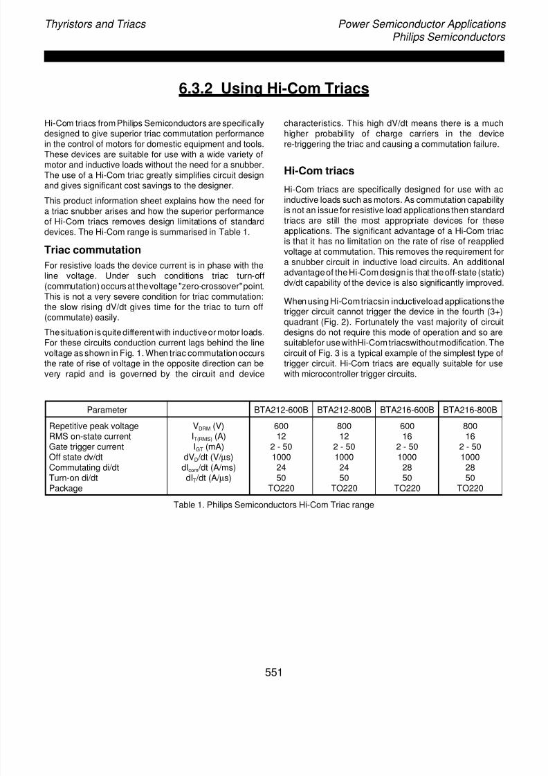
7/25/2019 Thyristors and Triacs
http://slidepdf.com/reader/full/thyristors-and-triacs 67/84
Thyristors and Triacs Power Semiconductor Applications Philips Semiconductors
6.3.2 Using Hi-Com Triacs
Hi-Com triacs from Philips Semiconductors are specifically
designed to give superior triac commutation performancein the control of motors for domestic equipment and tools.These devices are suitable for use with a wide variety ofmotor and inductive loads without the need for a snubber.The use of a Hi-Com triac greatly simplifies circuit designand gives significant cost savings to the designer.
This product information sheet explains how the need fora triac snubber arises and how the superior performanceof Hi-Com triacs removes design limitations of standarddevices. The Hi-Com range is summarised in Table 1.
Triac commutation
For resistive loads the device current is in phase with theline voltage. Under such conditions triac turn-off(commutation)occurs at thevoltage "zero-crossover"point.This is not a very severe condition for triac commutation:the slow rising dV/dt gives time for the triac to turn off(commutate) easily.
Thesituation is quite different with inductiveor motor loads.For these circuits conduction current lags behind the linevoltage as shown in Fig. 1. When triac commutation occursthe rate of rise of voltage in the opposite direction can bevery rapid and is governed by the circuit and device
characteristics. This high dV/dt means there is a much
higher probability of charge carriers in the devicere-triggering the triac and causing a commutation failure.
Hi-Com triacs
Hi-Com triacs are specifically designed for use with acinductive loads such as motors. As commutation capabilityis not an issue for resistive load applications then standardtriacs are still the most appropriate devices for theseapplications. The significant advantage of a Hi-Com triacis that it has no limitation on the rate of rise of reappliedvoltage at commutation. This removes the requirement fora snubber circuit in inductive load circuits. An additional
advantageof the Hi-Com design is that theoff-state (static)dv/dt capability of the device is also significantly improved.
When using Hi-Comtriacsin inductiveload applicationsthetrigger circuit cannot trigger the device in the fourth (3+)quadrant (Fig. 2). Fortunately the vast majority of circuitdesigns do not require this mode of operation and so aresuitablefor usewithHi-Comtriacswithoutmodification. Thecircuit of Fig. 3 is a typical example of the simplest type oftrigger circuit. Hi-Com triacs are equally suitable for usewith microcontroller trigger circuits.
Parameter BTA212-600B BTA212-800B BTA216-600B BTA216-800B
Repetitive peak voltage VDRM (V) 600 800 600 800RMS on-state current IT(RMS) (A) 12 12 16 16Gate trigger current IGT (mA) 2 - 50 2 - 50 2 - 50 2 - 50Off state dv/dt dVD /dt (V/ µs) 1000 1000 1000 1000Commutating di/dt dIcom /dt (A/ms) 24 24 28 28Turn-on di/dt dIT /dt (A/ µs) 50 50 50 50Package TO220 TO220 TO220 TO220
Table 1. Philips Semiconductors Hi-Com Triac range
551
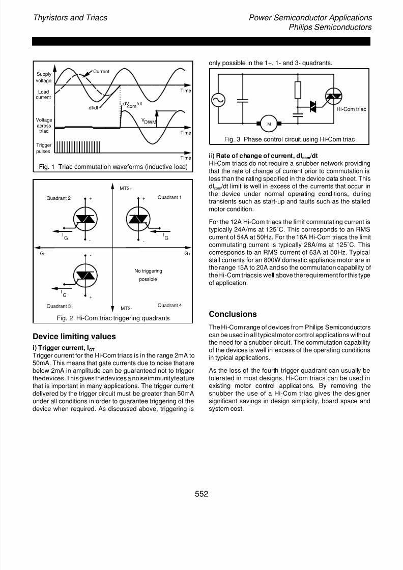
7/25/2019 Thyristors and Triacs
http://slidepdf.com/reader/full/thyristors-and-triacs 68/84
Thyristors and Triacs Power Semiconductor Applications Philips Semiconductors
Fig. 1 Triac commutation waveforms (inductive load)
Fig. 2 Hi-Com triac triggering quadrants
Device limiting values
i) Trigger current, IGT
Trigger current for the Hi-Com triacs is in the range 2mA to50mA. This means that gate currents due to noise that arebelow 2mA in amplitude can be guaranteed not to triggerthedevices.Thisgives thedevicesa noiseimmunityfeaturethat is important in many applications. The trigger currentdelivered by the trigger circuit must be greater than 50mA
under all conditions in order to guarantee triggering of thedevice when required. As discussed above, triggering is
only possible in the 1+, 1- and 3- quadrants.
Fig. 3 Phase control circuit using Hi-Com triac
ii) Rate of change of current, dIcom/dtHi-Com triacs do not require a snubber network providingthat the rate of change of current prior to commutation isless than the rating specified in the device data sheet. ThisdIcom /dt limit is well in excess of the currents that occur inthe device under normal operating conditions, during
transients such as start-up and faults such as the stalledmotor condition.
For the 12A Hi-Com triacs the limit commutating current istypically 24A/ms at 125˚C. This corresponds to an RMScurrent of 54A at 50Hz. For the 16A Hi-Com triacs the limitcommutating current is typically 28A/ms at 125˚C. Thiscorresponds to an RMS current of 63A at 50Hz. Typicalstall currents for an 800W domestic appliance motor are inthe range 15A to 20A and so the commutation capability oftheHi-Com triacsis well above therequirement for this typeof application.
Conclusions
TheHi-Com range of devices from Philips Semiconductorscan be used in all typical motor control applications withoutthe need for a snubber circuit. The commutation capabilityof the devices is well in excess of the operating conditionsin typical applications.
As the loss of the fourth trigger quadrant can usually betolerated in most designs, Hi-Com triacs can be used inexisting motor control applications. By removing thesnubber the use of a Hi-Com triac gives the designer
significant savings in design simplicity, board space andsystem cost.
VDWM
-dI/dtdV
com /dt
Time
Time
Time
Supply
voltage
Loadcurrent
Voltageacrosstriac
Trigger
pulses
Current
Hi-Com triac
M
Quadrant 1Quadrant 2
Quadrant 4Quadrant 3
G+G-
MT2+
MT2-
IG
IG
IG
++
- -
+
-
No triggering
possible
552

7/25/2019 Thyristors and Triacs
http://slidepdf.com/reader/full/thyristors-and-triacs 69/84
Preface Power Semiconductor ApplicationsPhilips Semiconductors
Acknowledgments
We are grateful for all the contributions from our colleagues within Philips and to the Application Laboratories in Eindhovenand Hamburg.
We would also like to thank Dr.P.H.Mellor of the University of Sheffield for contributing the application note of section 3.1.5.
The authors thank Mrs.R.Hayes for her considerable help in the preparation of this book.
The authors also thank Mr.D.F.Haslam for his assistance in the formatting and printing of the manuscripts.
Contributing Authors
N.Bennett
M.Bennion
D.Brown
C.Buethker
L.Burley
G.M.Fry
R.P.Gant
J.Gilliam
D.Grant
N.J.Ham
C.J.Hammerton
D.J.Harper
W.Hettersheid
J.v.d.Hooff
J.Houldsworth
M.J.Humphreys
P.H.Mellor
R.Miller
H.Misdom
P.Moody
S.A.Mulder
E.B.G. Nijhof
J.Oosterling
N.Pichowicz
W.B.Rosink
D.C. de Ruiter
D.Sharples
H.Simons
T.Stork
D.Tebb
H.Verhees
F.A.Woodworth
T.van de Wouw
This book was originally prepared by the Power Semiconductor Applications Laboratory, of the Philips Semiconductorsproduct division, Hazel Grove:
M.J.Humphreys
C.J.Hammerton
D.Brown
R.Miller
L.Burley
It was revised and updated, in 1994, by:
N.J.Ham C.J.Hammerton D.Sharples

7/25/2019 Thyristors and Triacs
http://slidepdf.com/reader/full/thyristors-and-triacs 70/84
Preface Power Semiconductor ApplicationsPhilips Semiconductors
Preface
This book was prepared by the Power Semiconductor Applications Laboratory of the Philips Semiconductors productdivision, Hazel Grove. Thebook is intended as a guide to using power semiconductors both efficiently and reliably in powerconversion applications. It is made up of eight main chapters each of which contains a number of application notes aimedat making it easier to select and use power semiconductors.
CHAPTER 1 forms an introduction to power semiconductors concentrating particularly on the two major power transistortechnologies, Power MOSFETs and High Voltage Bipolar Transistors.
CHAPTER 2 is devoted to Switched Mode Power Supplies. It begins with a basic description of the most commonly usedtopologies and discusses the major issues surrounding the use of power semiconductors including rectifiers. Specificdesign examples are given as well as a look at designing the magnetic components. The end of this chapter describesresonant power supply technology.
CHAPTER 3 describes motion control in terms of ac, dc and stepper motor operation and control. This chapter looks onlyat transistor controls, phase control using thyristors and triacs is discussed separately in chapter 6.
CHAPTER 4 looks at television and monitor applications. A description of the operation of horizontal deflection circuits isgiven followed by transistor selection guidesforboth deflection andpower supply applications. Deflection and power supply
circuitexamplesarealso givenbasedon circuitsdesignedby theProduct ConceptandApplication Laboratories (Eindhoven).
CHAPTER 5 concentrates on automotive electronics looking in detail at the requirements for the electronic switches takinginto consideration the harsh environment in which they must operate.
CHAPTER 6 reviews thyristor andtriac applicationsfrom thebasicsof device technology andoperation to the simpledesignrules which should be followed to achieve maximum reliability. Specific examples are given in this chapter for a numberof the common applications.
CHAPTER 7 looks at the thermal considerations for power semiconductors in terms of power dissipation and junctiontemperature limits. Part of this chapter is devoted to workedexamplesshowing howjunction temperaturescanbecalculatedto ensure the limits are not exceeded. Heatsink requirements and designs are also discussed in the second half of thischapter.
CHAPTER 8 is an introduction to the use of high voltage bipolar transistors in electronic lighting ballasts. Many of the
possible topologies are described.

7/25/2019 Thyristors and Triacs
http://slidepdf.com/reader/full/thyristors-and-triacs 71/84
Contents Power Semiconductor ApplicationsPhilips Semiconductors
Table of Contents
CHAPTER 1 Introduction to Power Semiconductors 1
General 3
1.1.1 An Introduction To Power Devices ............................................................ 5
Power MOSFET 17
1.2.1 PowerMOS Introduction ............................................................................. 19
1.2.2 Understanding Power MOSFET Switching Behaviour ............................... 29
1.2.3 Power MOSFET Drive Circuits .................................................................. 39
1.2.4 Parallel Operation of Power MOSFETs ..................................................... 49
1.2.5 Series Operation of Power MOSFETs ....................................................... 53
1.2.6 Logic Level FETS ...................................................................................... 57
1.2.7 Avalanche Ruggedness ............................................................................. 61
1.2.8 Electrostatic Discharge (ESD) Considerations .......................................... 67
1.2.9 Understanding the Data Sheet: PowerMOS .............................................. 69
High Voltage Bipolar Transistor 77
1.3.1 Introduction To High Voltage Bipolar Transistors ...................................... 79
1.3.2 Effects of Base Drive on Switching Times ................................................. 83
1.3.3 Using High Voltage Bipolar Transistors ..................................................... 911.3.4 Understanding The Data Sheet: High Voltage Transistors ....................... 97
CHAPTER 2 Switched Mode Power Supplies 103
Using Power Semiconductors in Switched Mode Topologies 105
2.1.1 An Introduction to Switched Mode Power Supply Topologies ................... 107
2.1.2 The Power Supply Designer’s Guide to High Voltage Transistors ............ 129
2.1.3 Base Circuit Design for High Voltage Bipolar Transistors in PowerConverters ........................................................................................................... 141
2.1.4 Isolated Power Semiconductors for High Frequency Power SupplyApplications ......................................................................................................... 153
Output Rectification 159
2.2.1 Fast Recovery Epitaxial Diodes for use in High Frequency Rectification 161
2.2.2 Schottky Diodes from Philips Semiconductors .......................................... 173
2.2.3 An Introduction to Synchronous Rectifier Circuits using PowerMOSTransistors ........................................................................................................... 179
i
7/25/2019 Thyristors and Triacs
http://slidepdf.com/reader/full/thyristors-and-triacs 72/84
Contents Power Semiconductor ApplicationsPhilips Semiconductors
Design Examples 185
2.3.1 Mains Input 100 W Forward Converter SMPS: MOSFET and BipolarTransistor Solutions featuring ETD Cores ........................................................... 187
2.3.2 Flexible, Low Cost, Self-Oscillating Power Supply using an ETD34Two-Part Coil Former and 3C85 Ferrite .............................................................. 199
Magnetics Design 205
2.4.1 Improved Ferrite Materials and Core Outlines for High Frequency PowerSupplies ............................................................................................................... 207
Resonant Power Supplies 217
2.5.1. An Introduction To Resonant Power Supplies .......................................... 219
2.5.2. Resonant Power Supply Converters - The Solution For Mains PollutionProblems .............................................................................................................. 225
CHAPTER 3 Motor Control 241
AC Motor Control 243
3.1.1 Noiseless A.C. Motor Control: Introduction to a 20 kHz System ............... 245
3.1.2 The Effect of a MOSFET’s Peak to Average Current Rating on InvertorEfficiency ............................................................................................................. 251
3.1.3 MOSFETs and FREDFETs for Motor Drive Equipment ............................. 253
3.1.4 A Designers Guide to PowerMOS Devices for Motor Control ................... 2593.1.5 A 300V, 40A High Frequency Inverter Pole Using Paralleled FREDFETModules ............................................................................................................... 273
DC Motor Control 283
3.2.1 Chopper circuits for DC motor control ....................................................... 285
3.2.2 A switched-mode controller for DC motors ................................................ 293
3.2.3 Brushless DC Motor Systems .................................................................... 301
Stepper Motor Control 307
3.3.1 Stepper Motor Control ............................................................................... 309
CHAPTER 4 Televisions and Monitors 317
Power Devices in TV & Monitor Applications (including selection guides) 319
4.1.1 An Introduction to Horizontal Deflection .................................................... 321
4.1.2 The BU25XXA/D Range of Deflection Transistors .................................... 331
ii
7/25/2019 Thyristors and Triacs
http://slidepdf.com/reader/full/thyristors-and-triacs 73/84
Contents Power Semiconductor ApplicationsPhilips Semiconductors
4.1.3 Philips HVT’s for TV & Monitor Applications .............................................. 339
4.1.4 TV and Monitor Damper Diodes ................................................................ 345
TV Deflection Circuit Examples 349
4.2.1 Application Information for the 16 kHz Black Line Picture Tubes .............. 351
4.2.2 32 kHz / 100 Hz Deflection Circuits for the 66FS Black Line Picture Tube 361
SMPS Circuit Examples 377
4.3.1 A 70W Full Performance TV SMPS Using The TDA8380 ......................... 379
4.3.2 A Synchronous 200W SMPS for 16 and 32 kHz TV .................................. 389
Monitor Deflection Circuit Example 397
4.4.1 A Versatile 30 - 64 kHz Autosync Monitor ................................................. 399
CHAPTER 5 Automotive Power Electronics 421
Automotive Motor Control (including selection guides) 423
5.1.1 Automotive Motor Control With Philips MOSFETS .................................... 425
Automotive Lamp Control (including selection guides) 433
5.2.1 Automotive Lamp Control With Philips MOSFETS .................................... 435
The TOPFET 443
5.3.1 An Introduction to the 3 pin TOPFET ......................................................... 445
5.3.2 An Introduction to the 5 pin TOPFET ......................................................... 447
5.3.3 BUK101-50DL - a Microcontroller compatible TOPFET ............................ 449
5.3.4 Protection with 5 pin TOPFETs ................................................................. 451
5.3.5 Driving TOPFETs ....................................................................................... 453
5.3.6 High Side PWM Lamp Dimmer using TOPFET ......................................... 455
5.3.7 Linear Control with TOPFET ...................................................................... 457
5.3.8 PWM Control with TOPFET ....................................................................... 459
5.3.9 Isolated Drive for TOPFET ........................................................................ 461
5.3.10 3 pin and 5 pin TOPFET Leadforms ........................................................ 463
5.3.11 TOPFET Input Voltage ............................................................................ 465
5.3.12 Negative Input and TOPFET ................................................................... 467
5.3.13 Switching Inductive Loads with TOPFET ................................................. 469
5.3.14 Driving DC Motors with TOPFET ............................................................. 471
5.3.15 An Introduction to the High Side TOPFET ............................................... 473
5.3.16 High Side Linear Drive with TOPFET ...................................................... 475
iii
7/25/2019 Thyristors and Triacs
http://slidepdf.com/reader/full/thyristors-and-triacs 74/84
Contents Power Semiconductor ApplicationsPhilips Semiconductors
Automotive Ignition 477
5.4.1 An Introduction to Electronic Automotive Ignition ...................................... 479
5.4.2 IGBTs for Automotive Ignition .................................................................... 481
5.4.3 Electronic Switches for Automotive Ignition ............................................... 483
CHAPTER 6 Power Control with Thyristors and Triacs 485
Using Thyristors and Triacs 487
6.1.1 Introduction to Thyristors and Triacs ......................................................... 489
6.1.2 Using Thyristors and Triacs ....................................................................... 497
6.1.3 The Peak Current Handling Capability of Thyristors .................................. 505
6.1.4 Understanding Thyristor and Triac Data .................................................... 509
Thyristor and Triac Applications 521
6.2.1 Triac Control of DC Inductive Loads .......................................................... 523
6.2.2 Domestic Power Control with Triacs and Thyristors .................................. 527
6.2.3 Design of a Time Proportional Temperature Controller ............................. 537
Hi-Com Triacs 547
6.3.1 Understanding Hi-Com Triacs ................................................................... 549
6.3.2 Using Hi-Com Triacs .................................................................................. 551
CHAPTER 7 Thermal Management 553
Thermal Considerations 555
7.1.1 Thermal Considerations for Power Semiconductors ................................. 557
7.1.2 Heat Dissipation ......................................................................................... 567
CHAPTER 8 Lighting 575
Fluorescent Lamp Control 577
8.1.1 Efficient Fluorescent Lighting using Electronic Ballasts ............................. 579
8.1.2 Electronic Ballasts - Philips Transistor Selection Guide ............................ 587
8.1.3 An Electronic Ballast - Base Drive Optimisation ........................................ 589
iv

7/25/2019 Thyristors and Triacs
http://slidepdf.com/reader/full/thyristors-and-triacs 75/84
Index Power Semiconductor ApplicationsPhilips Semiconductors
Index
Airgap, transformer core, 111, 113Anti saturation diode, 590Asynchronous, 497
Automotivefanssee motor control
IGBT, 481, 483ignition, 479, 481, 483lamps, 435, 455motor control, 425, 457, 459, 471, 475resistive loads, 442reverse battery, 452, 473, 479screen heater, 442seat heater, 442solenoids, 469TOPFET, 473
Avalanche, 61Avalanche breakdown
thyristor, 490Avalanche multiplication, 134
Baker clamp, 138, 187, 190Ballast
electronic, 580fluorescent lamp, 579switchstart, 579
Base drive, 136base inductor, 147
base inductor, diode assisted, 148base resistor, 146drive transformer, 145drive transformer leakage inductance, 149electronic ballast, 589forward converter, 187power converters, 141speed-up capacitor, 143
Base inductor, 144, 147Base inductor, diode assisted, 148Boost converter, 109
continuous mode, 109discontinuous mode, 109
output ripple, 109Bootstrap, 303Breakback voltage
diac, 492Breakdown voltage, 70Breakover current
diac, 492Breakover voltage
diac, 492, 592thyristor, 490
Bridge circuitssee Motor Control - AC
Brushless motor, 301, 303
Buck-boost converter, 110Buck converter, 108 - 109Burst firing, 537Burst pulses, 564
Capacitance junction, 29
Capacitormains dropper, 544
CENELEC, 537Charge carriers, 133
triac commutation, 549Choke
fluorescent lamp, 580Choppers, 285Clamp diode, 117Clamp winding, 113Commutation
diode, 164Hi-Com triac, 551thyristor, 492triac, 494, 523, 529
Compact fluorescent lamp, 585Continuous mode
see Switched Mode Power Supplies
Continuous operation, 557Converter (dc-dc)switched mode power supply, 107
Cookers, 537Cooling
forced, 572natural, 570
Crest factor, 529Critical electric field, 134Cross regulation, 114, 117Current fed resonant inverter, 589Current Mode Control, 120Current tail, 138, 143
Damper Diodes, 345, 367forward recovery, 328, 348losses, 347outlines, 345picture distortion, 328, 348selection guide, 345
Darlington, 13Data Sheets
High Voltage Bipolar Transistor, 92,97,331MOSFET, 69
i

7/25/2019 Thyristors and Triacs
http://slidepdf.com/reader/full/thyristors-and-triacs 76/84
Index Power Semiconductor ApplicationsPhilips Semiconductors
dc-dc converter, 119Depletion region, 133Desaturation networks, 86
Baker clamp, 91, 138dI/dt
triac, 531Diac, 492, 500, 527, 530, 591Diode, 6
double diffused, 162epitaxial, 161schottky, 173structure, 161
Diode Modulator, 327, 367Disc drives, 302Discontinuous mode
see Switched Mode Power SuppliesDomestic Appliances, 527Dropper
capacitive, 544resistive, 544, 545Duty cycle, 561
EFD coresee magnetics
Efficiency Diodessee Damper Diodes
Electric drill, 531Electronic ballast, 580
base drive optimisation, 589current fed half bridge, 584, 587, 589current fed push pull, 583, 587flyback, 582transistor selection guide, 587voltage fed half bridge, 584, 588voltage fed push pull, 583, 587
EMC, 260, 455see RFI, ESDTOPFET, 473
Emitter shortingtriac, 549
Epitaxial diode, 161characteristics, 163dI/dt, 164
forward recovery, 168lifetime control, 162operating frequency, 165passivation, 162reverse leakage, 169reverse recovery, 162, 164reverse recovery softness, 167selection guide, 171snap-off, 167softness factor, 167stored charge, 162technology, 162
ESD, 67see Protection, ESDprecautions, 67
ETD coresee magnetics
F-packsee isolated package
Fall time, 143, 144Fast Recovery Epitaxial Diode (FRED)
see epitaxial diodeFBSOA, 134Ferrites
see magneticsFlicker
fluorescent lamp, 580Fluorescent lamp, 579
colour rendering, 579
colour temperature, 579efficacy, 579, 580triphosphor, 579
Flyback converter, 110, 111, 113advantages, 114clamp winding, 113continuous mode, 114coupled inductor, 113cross regulation, 114diodes, 115disadvantages, 114discontinuous mode, 114electronic ballast, 582leakage inductance, 113magnetics, 213operation, 113rectifier circuit, 180self oscillating power supply, 199synchronous rectifier, 156, 181transformer core airgap, 111, 113transistors, 115
Flyback converter (two transistor), 111, 114Food mixer, 531Forward converter, 111, 116
advantages, 116
clamp diode, 117conduction loss, 197continuous mode, 116core loss, 116core saturation, 117cross regulation, 117diodes, 118disadvantages, 117duty ratio, 117ferrite cores, 116magnetics, 213magnetisation energy, 116, 117
ii

7/25/2019 Thyristors and Triacs
http://slidepdf.com/reader/full/thyristors-and-triacs 77/84
Index Power Semiconductor ApplicationsPhilips Semiconductors
operation, 116output diodes, 117output ripple, 116rectifier circuit, 180reset winding, 117
switched mode power supply, 187switching frequency, 195switching losses, 196synchronous rectifier, 157, 181transistors, 118
Forward converter (two transistor), 111, 117Forward recovery, 168FREDFET, 250, 253, 305
bridge circuit, 255charge, 254diode, 254drive, 262loss, 256
reverse recovery, 254FREDFETsmotor control, 259
Full bridge converter, 111, 125advantages, 125diodes, 126disadvantages, 125operation, 125transistors, 126
Gatetriac, 538
Gate driveforward converter, 195
Gold doping, 162, 169GTO, 11Guard ring
schottky diode, 174
Half bridge, 253Half bridge circuits
see also Motor Control - ACHalf bridge converter, 111, 122
advantages, 122clamp diodes, 122
cross conduction, 122diodes, 124disadvantages, 122electronic ballast, 584, 587, 589flux symmetry, 122magnetics, 214operation, 122synchronous rectifier, 157transistor voltage, 122transistors, 124voltage doubling, 122
Heat dissipation, 567
Heat sink compound, 567Heater controller, 544Heaters, 537Heatsink, 569Heatsink compound, 514
Hi-Com triac, 519, 549, 551commutation, 551dIcom/dt, 552gate trigger current, 552inductive load control, 551
High side switchMOSFET, 44, 436TOPFET, 430, 473
High Voltage Bipolar Transistor, 8, 79, 91,141, 341
‘bathtub’ curves, 333avalanche breakdown, 131avalanche multiplication, 134
Baker clamp, 91, 138base-emitter breakdown, 144base drive, 83, 92, 96, 136, 336, 385base drive circuit, 145base inductor, 138, 144, 147base inductor, diode assisted, 148base resistor, 146breakdown voltage, 79, 86, 92carrier concentration, 151carrier injection, 150conductivity modulation, 135, 150critical electric field, 134current crowding, 135, 136current limiting values, 132current tail, 138, 143current tails, 86, 91d-type, 346data sheet, 92, 97, 331depletion region, 133desaturation, 86, 88, 91device construction, 79dI/dt, 139drive transformer, 145drive transformer leakage inductance, 149dV/dt, 139
electric field, 133electronic ballast, 581, 585, 587, 589Fact Sheets, 334fall time, 86, 99, 143, 144FBSOA, 92, 99, 134hard turn-off, 86horizontal deflection, 321, 331, 341leakage current, 98limiting values, 97losses, 92, 333, 342Miller capacitance, 139operation, 150
iii

7/25/2019 Thyristors and Triacs
http://slidepdf.com/reader/full/thyristors-and-triacs 78/84
Index Power Semiconductor ApplicationsPhilips Semiconductors
optimum drive, 88outlines, 332, 346over current, 92, 98over voltage, 92, 97overdrive, 85, 88, 137, 138
passivation, 131power limiting value, 132process technology, 80ratings, 97RBSOA, 93, 99, 135, 138, 139RC network, 148reverse recovery, 143, 151safe operating area, 99, 134saturation, 150saturation current, 79, 98, 341secondary breakdown, 92, 133smooth turn-off, 86SMPS, 94, 339, 383
snubber, 139space charge, 133speed-up capacitor, 143storage time, 86, 91, 92, 99, 138, 144, 342sub emitter resistance, 135switching, 80, 83, 86, 91, 98, 342technology, 129, 149thermal breakdown, 134thermal runaway, 152turn-off, 91, 92, 138, 142, 146, 151turn-on, 91, 136, 141, 149, 150underdrive, 85, 88voltage limiting values, 130
Horizontal Deflection, 321, 367base drive, 336control ic, 401d-type transistors, 346damper diodes, 345, 367diode modulator, 327, 347, 352, 367drive circuit, 352, 365, 406east-west correction, 325, 352, 367line output transformer, 354linearity correction, 323operating cycle, 321, 332, 347s-correction, 323, 352, 404
TDA2595, 364, 368TDA4851, 400TDA8433, 363, 369test circuit, 321transistors, 331, 341, 408waveforms, 322
IGBT, 11, 305automotive, 481, 483clamped, 482, 484ignition, 481, 483
Ignitionautomotive, 479, 481, 483darlington, 483
Induction heating, 53Induction motor
see Motor Control - ACInductive loadsee Solenoid
Inrush current, 528, 530Intrinsic silicon, 133Inverter, 260, 273
see motor control accurrent fed, 52, 53switched mode power supply, 107
Irons, electric, 537Isolated package, 154
stray capacitance, 154, 155thermal resistance, 154
Isolation, 153
J-FET, 9Junction temperature, 470, 557, 561
burst pulses, 564non-rectangular pulse, 565rectangular pulse, composite, 562rectangular pulse, periodic, 561rectangular pulse, single shot, 561
Lamp dimmer, 530Lamps, 435
dI/dt, 438inrush current, 438MOSFET, 435PWM control, 455switch rate, 438TOPFET, 455
Latching currentthyristor, 490
Leakage inductance, 113, 200, 523Lifetime control, 162Lighting
fluorescent, 579phase control, 530
Logic Level FETmotor control, 432Logic level MOSFET, 436
Magnetics, 207100W 100kHz forward converter, 197100W 50kHz forward converter, 19150W flyback converter, 199core losses, 208core materials, 207EFD core, 210ETD core, 199, 207
iv

7/25/2019 Thyristors and Triacs
http://slidepdf.com/reader/full/thyristors-and-triacs 79/84
Index Power Semiconductor ApplicationsPhilips Semiconductors
flyback converter, 213forward converter, 213half bridge converter, 214power density, 211push-pull converter, 213
switched mode power supply, 187switching frequency, 215transformer construction, 215
Mains Flicker, 537Mains pollution, 225
pre-converter, 225Mains transient, 544Mesa glass, 162Metal Oxide Varistor (MOV), 503Miller capacitance, 139Modelling, 236, 265MOS Controlled Thyristor, 13MOSFET, 9, 19, 153, 253
bootstrap, 303breakdown voltage, 22, 70capacitance, 30, 57, 72, 155, 156capacitances, 24characteristics, 23, 70 - 72charge, 32, 57data sheet, 69dI/dt, 36diode, 253drive, 262, 264drive circuit loss, 156driving, 39, 250dV/dt, 36, 39, 264ESD, 67gate-source protection, 264gate charge, 195gate drive, 195gate resistor, 156high side, 436high side drive, 44inductive load, 62lamps, 435leakage current, 71linear mode, parallelling, 52logic level, 37, 57, 305
loss, 26, 34maximum current, 69motor control, 259, 429modelling, 265on-resistance, 21, 71package inductance, 49, 73parallel operation, 26, 47, 49, 265parasitic oscillations, 51peak current rating, 251Resonant supply, 53reverse diode, 73ruggedness, 61, 73
safe operating area, 25, 74series operation, 53SMPS, 339, 384solenoid, 62structure, 19
switching, 24, 29, 58, 73, 194, 262switching loss, 196synchronous rectifier, 179thermal impedance, 74thermal resistance, 70threshold voltage, 21, 70transconductance, 57, 72turn-off, 34, 36turn-on, 32, 34, 35, 155, 256
Motor, universalback EMF, 531starting, 528
Motor Control - AC, 245, 273
anti-parallel diode, 253antiparallel diode, 250carrier frequency, 245control, 248current rating, 262dc link, 249diode, 261diode recovery, 250duty ratio, 246efficiency, 262EMC, 260filter, 250FREDFET, 250, 259, 276gate drives, 249half bridge, 245inverter, 250, 260, 273line voltage, 262loss, 267MOSFET, 259Parallel MOSFETs, 276peak current, 251phase voltage, 262power factor, 262pulse width modulation, 245, 260ripple, 246
short circuit, 251signal isolation, 250snubber, 276speed control, 248switching frequency, 246three phase bridge, 246underlap, 248
Motor Control - DC, 285, 293, 425braking, 285, 299brushless, 301control, 290, 295, 303current rating, 288
v

7/25/2019 Thyristors and Triacs
http://slidepdf.com/reader/full/thyristors-and-triacs 80/84
Index Power Semiconductor ApplicationsPhilips Semiconductors
drive, 303duty cycle, 286efficiency, 293FREDFET, 287freewheel diode, 286
full bridge, 287half bridge, 287high side switch, 429IGBT, 305inrush, 430inverter, 302linear, 457, 475logic level FET, 432loss, 288MOSFET, 287, 429motor current, 295overload, 430permanent magnet, 293, 301
permanent magnet motor, 285PWM, 286, 293, 459, 471servo, 298short circuit, 431stall, 431TOPFET, 430, 457, 459, 475topologies, 286torque, 285, 294triac, 525voltage rating, 288
Motor Control - Stepper, 309bipolar, 310chopper, 314drive, 313hybrid, 312permanent magnet, 309reluctance, 311step angle, 309unipolar, 310
Mounting, transistor, 154Mounting base temperature, 557Mounting torque, 514
Parasitic oscillation, 149Passivation, 131, 162
PCB Design, 368, 419Phase angle, 500Phase control, 546
thyristors and triacs, 498triac, 523
Phase voltagesee motor control - ac
Power dissipation, 557see High Voltage Bipolar Transistor loss,MOSFET loss
Power factor correction, 580active, boost converted, 581
Power MOSFETsee MOSFET
Proportional control, 537Protection
ESD, 446, 448, 482
overvoltage, 446, 448, 469reverse battery, 452, 473, 479short circuit, 251, 446, 448temperature, 446, 447, 471TOPFET, 445, 447, 451
Pulse operation, 558Pulse Width Modulation (PWM), 108Push-pull converter, 111, 119
advantages, 119clamp diodes, 119cross conduction, 119current mode control, 120diodes, 121
disadvantages, 119duty ratio, 119electronic ballast, 582, 587flux symmetry, 119, 120magnetics, 213multiple outputs, 119operation, 119output filter, 119output ripple, 119rectifier circuit, 180switching frequency, 119transformer, 119transistor voltage, 119transistors, 121
Qs (stored charge), 162
RBSOA, 93, 99, 135, 138, 139Rectification, synchronous, 179Reset winding, 117Resistor
mains dropper, 544, 545Resonant power supply, 219, 225
modelling, 236MOSFET, 52, 53
pre-converter, 225Reverse leakage, 169Reverse recovery, 143, 162RFI, 154, 158, 167, 393, 396, 497, 529, 530,537Ruggedness
MOSFET, 62, 73schottky diode, 173
Safe Operating Area (SOA), 25, 74, 134, 557forward biased, 92, 99, 134reverse biased, 93, 99, 135, 138, 139
vi

7/25/2019 Thyristors and Triacs
http://slidepdf.com/reader/full/thyristors-and-triacs 81/84
Index Power Semiconductor ApplicationsPhilips Semiconductors
Saturable choketriac, 523
Schottky diode, 173bulk leakage, 174edge leakage, 174
guard ring, 174reverse leakage, 174ruggedness, 173selection guide, 176technology, 173
SCRsee Thyristor
Secondary breakdown, 133Selection Guides
BU25XXA, 331BU25XXD, 331damper diodes, 345EPI diodes, 171
horizontal deflection, 343MOSFETs driving heaters, 442MOSFETs driving lamps, 441MOSFETs driving motors, 426Schottky diodes, 176SMPS, 339
Self Oscillating Power Supply (SOPS)50W microcomputer flyback converter, 199ETD transformer, 199
Servo, 298Single ended push-pull
see half bridge converterSnap-off, 167Snubber, 93, 139, 495, 502, 523, 529, 549
active, 279Softness factor, 167Solenoid
TOPFET, 469, 473turn off, 469, 473
Solid state relay, 501SOT186, 154SOT186A, 154SOT199, 154Space charge, 133Speed-up capacitor, 143
Speed controlthyristor, 531triac, 527
Starterfluorescent lamp, 580
Startup circuitelectronic ballast, 591self oscillating power supply, 201
Static Induction Thyristor, 11Stepdown converter, 109Stepper motor, 309Stepup converter, 109
Storage time, 144Stored charge, 162Suppression
mains transient, 544Switched Mode Power Supply (SMPS)
see also self oscillating power supply100W 100kHz MOSFET forward converter,192100W 500kHz half bridge converter, 153100W 50kHz bipolar forward converter, 18716 & 32 kHz TV, 389asymmetrical, 111, 113base circuit design, 149boost converter, 109buck-boost converter, 110buck converter, 108ceramic output filter, 153continuous mode, 109, 379
control ic, 391control loop, 108core excitation, 113core loss, 167current mode control, 120dc-dc converter, 119diode loss, 166diode reverse recovery effects, 166diode reverse recovery softness, 167diodes, 115, 118, 121, 124, 126discontinuous mode, 109, 379epitaxial diodes, 112, 161flux swing, 111flyback converter, 92, 111, 113, 123forward converter, 111, 116, 379full bridge converter, 111, 125half bridge converter, 111, 122high voltage bipolar transistor, 94, 112, 115,118, 121, 124, 126, 129, 339, 383, 392isolated, 113isolated packages, 153isolation, 108, 111magnetics design, 191, 197magnetisation energy, 113mains filter, 380
mains input, 390MOSFET, 112, 153, 33, 384multiple output, 111, 156non-isolated, 108opto-coupler, 392output rectifiers, 163parasitic oscillation, 149power-down, 136power-up, 136, 137, 139power MOSFET, 153, 339, 384pulse width modulation, 108push-pull converter, 111, 119
vii

7/25/2019 Thyristors and Triacs
http://slidepdf.com/reader/full/thyristors-and-triacs 82/84
Index Power Semiconductor ApplicationsPhilips Semiconductors
RBSOA failure, 139rectification, 381, 392rectification efficiency, 163rectifier selection, 112regulation, 108
reliability, 139resonantsee resonant power supply
RFI, 154, 158, 167schottky diode, 112, 154, 173snubber, 93, 139, 383soft start, 138standby, 382standby supply, 392start-up, 391stepdown, 109stepup, 109symmetrical, 111, 119, 122
synchronisation, 382synchronous rectification, 156, 179TDA8380, 381, 391topologies, 107topology output powers, 111transformer, 111transformer saturation, 138transformers, 391transistor current limiting value, 112transistor mounting, 154transistor selection, 112transistor turn-off, 138transistor turn-on, 136transistor voltage limiting value, 112transistors, 115, 118, 121, 124, 126turns ratio, 111TV & Monitors, 339, 379, 399two transistor flyback, 111, 114two transistor forward, 111, 117
Switching loss, 230Synchronous, 497Synchronous rectification, 156, 179
self driven, 181transformer driven, 180
Temperature control, 537Thermalcontinuous operation, 557, 568intermittent operation, 568non-rectangular pulse, 565pulse operation, 558rectangular pulse, composite, 562rectangular pulse, periodic, 561rectangular pulse, single shot, 561single shot operation, 561
Thermal capacity, 558, 568
Thermal characteristicspower semiconductors, 557
Thermal impedance, 74, 568Thermal resistance, 70, 154, 557Thermal time constant, 568
Thyristor, 10, 497, 509’two transistor’ model, 490applications, 527asynchronous control, 497avalanche breakdown, 490breakover voltage, 490, 509cascading, 501commutation, 492control, 497current rating, 511dI/dt, 490dIf/dt, 491dV/dt, 490
energy handling, 505external commutation, 493full wave control, 499fusing I2t, 503, 512gate cathode resistor, 500gate circuits, 500gate current, 490gate power, 492gate requirements, 492gate specifications, 512gate triggering, 490half wave control, 499holding current, 490, 509inductive loads, 500inrush current, 503latching current, 490, 509leakage current, 490load line, 492mounting, 514operation, 490overcurrent, 503peak current, 505phase angle, 500phase control, 498, 527pulsed gate, 500
resistive loads, 498resonant circuit, 493reverse characteristic, 489reverse recovery, 493RFI, 497self commutation, 493series choke, 502snubber, 502speed controller, 531static switching, 497structure, 489switching, 489
viii

7/25/2019 Thyristors and Triacs
http://slidepdf.com/reader/full/thyristors-and-triacs 83/84
Index Power Semiconductor ApplicationsPhilips Semiconductors
switching characteristics, 517synchronous control, 497temperature rating, 512thermal specifications, 512time proportional control, 497
transient protection, 502trigger angle, 500turn-off time, 494turn-on, 490, 509turn-on dI/dt, 502varistor, 503voltage rating, 510
Thyristor data, 509Time proportional control, 537TOPFET
3 pin, 445, 449, 4615 pin, 447, 451, 457, 459, 463driving, 449, 453, 461, 465, 467, 475
high side, 473, 475lamps, 455leadforms, 463linear control, 451, 457motor control, 430, 457, 459negative input, 456, 465, 467protection, 445, 447, 451, 469, 473PWM control, 451, 455, 459solenoids, 469
Transformertriac controlled, 523
Transformer core airgap, 111, 113Transformers
see magneticsTransient thermal impedance, 559Transient thermal response, 154Triac, 497, 510, 518
400Hz operation, 489, 518applications, 527, 537asynchronous control, 497breakover voltage, 510charge carriers, 549commutating dI/dt, 494commutating dV/dt, 494commutation, 494, 518, 523, 529, 549
control, 497dc inductive load, 523dc motor control, 525dI/dt, 531, 549dIcom/dt, 523dV/dt, 523, 549emitter shorting, 549full wave control, 499fusing I2t, 503, 512gate cathode resistor, 500gate circuits, 500gate current, 491
gate requirements, 492gate resistor, 540, 545gate sensitivity, 491gate triggering, 538holding current, 491, 510
Hi-Com, 549, 551inductive loads, 500inrush current, 503isolated trigger, 501latching current, 491, 510operation, 491overcurrent, 503phase angle, 500phase control, 498, 527, 546protection, 544pulse triggering, 492pulsed gate, 500quadrants, 491, 510
resistive loads, 498RFI, 497saturable choke, 523series choke, 502snubber, 495, 502, 523, 529, 549speed controller, 527static switching, 497structure, 489switching, 489synchronous control, 497transformer load, 523transient protection, 502trigger angle, 492, 500triggering, 550turn-on dI/dt, 502varistor, 503zero crossing, 537
Trigger angle, 500TV & Monitors
16 kHz black line, 35130-64 kHz autosync, 39932 kHz black line, 361damper diodes, 345, 367diode modulator, 327, 367EHT, 352 - 354, 368, 409, 410
high voltage bipolar transistor, 339, 341horizontal deflection, 341picture distortion, 348power MOSFET, 339SMPS, 339, 354, 379, 389, 399vertical deflection, 358, 364, 402
Two transistor flyback converter, 111, 114Two transistor forward converter, 111, 117
Universal motorback EMF, 531
ix

7/25/2019 Thyristors and Triacs
http://slidepdf.com/reader/full/thyristors-and-triacs 84/84
Index Power Semiconductor ApplicationsPhilips Semiconductors
starting, 528
Vacuum cleaner, 527Varistor, 503Vertical Deflection, 358, 364, 402
Voltage doubling, 122Water heaters, 537
Zero crossing, 537Zero voltage switching, 537