the sca103t differential inclinometer series
TRANSCRIPT

SCA103T Series
Murata Electronics Oy Subject to changes 1/17
www.muratamems.fi Doc.Nr. 8261700 Rev.A3
Self test 2
Sensing
element 1
Sensing
element 2
SPI interface
Self test 1
Signal conditioning
and filtering
A/D conversion
Signal conditioning
and filtering
EEPROM
calibration
memory9 ST_2
10 ST_1
12 VDD
6 GND
11 OUT_1
5 OUT_2
1 SCK
3 MISO
4 MOSI
7 CSB
Temperature
Sensor
THE SCA103T DIFFERENTIAL INCLINOMETER SERIES The SCA103T Series is a 3D-MEMS-based single axis inclinometer family that uses the differential measurement principle. The high calibration accuracy combines extremely low temperature dependency, high resolution and low noise together with a robust sensing element design, to make the SCA103T an ideal choice for high accuracy leveling instruments. The Murata inclinometers are insensitive to vibration due to having over damped sensing elements plus they can withstand mechanical shocks of 20000 g.
Features
Measuring ranges ±15° SCA103T-D04 and ± 30° SCA103T-D05
0.001° resolution (10 Hz BW, analog output)
Sensing element controlled over damped frequency response (-3dB 18Hz)
Robust design, high shock durability (20000g)
Excellent stability over temperature and time
Common mode error and noise reduction using the differential measurement principle
Single +5 V supply
Ratiometric analog voltage outputs
Digital SPI inclination and temperature output
Comprehensive failure detection features o True self test by deflecting the sensing
elements’ proof mass by electrostatic force. o Continuous sensing element interconnection
failure check. o Continuous memory parity check.
RoHS compliant
Compatible with Pb-free reflow solder process
Applications
Platform leveling and stabilization
Rotating laser levels
Leveling instruments
Construction levels
Figure 1. Functional block diagram
Data Sheet
SCA103T Series
Murata Electronics Oy Subject to changes 2/17
www.muratamems.fi Doc.Nr. 8261700 Rev.A3
TABLE OF CONTENTS
The SCA103T Differential Inclinometer Series ....................................................................... 1
Features............................................................................................................................................. 1
Applications ...................................................................................................................................... 1
Table of Contents...................................................................................................................... 2
1 Electrical Specifications ..................................................................................................... 3
1.1 Absolute Maximum Ratings ................................................................................................... 3
1.2 Performance Characteristics .................................................................................................. 3
1.3 Electrical Characteristics ....................................................................................................... 4
1.4 SPI Interface DC Characteristics ............................................................................................ 4
1.5 SPI Interface AC Characteristics ............................................................................................ 4
1.6 SPI Interface Timing Specifications ....................................................................................... 5
1.7 Electrical Connection.............................................................................................................. 6
1.8 Typical Performance Characteristics .................................................................................... 6 1.8.1 Additional External Compensation ...................................................................................... 7
2 Functional Description ....................................................................................................... 8
2.1 Differential Measurement ....................................................................................................... 8
2.2 Voltage to Angle Conversion ................................................................................................. 9
2.3 Ratiometric Output ................................................................................................................ 10
2.4 SPI Serial Interface ................................................................................................................ 10
2.5 Digital Output to Angle Conversion ..................................................................................... 12
2.6 Self Test and Failure Detection Modes ................................................................................ 13
2.7 Temperature Measurement .................................................................................................. 14
3 Application Information .................................................................................................... 15
3.1 Recommended Circuit Diagrams and Printed Circuit Board Layouts ............................... 15
3.2 Recommended Printed Circuit Board Footprint ................................................................. 16
4 Mechanical Specifications and Reflow Soldering .......................................................... 16
4.1 Mechanical Specifications (Reference only) ....................................................................... 16
4.2 Reflow Soldering ................................................................................................................... 17

SCA103T Series
Murata Electronics Oy Subject to changes 3/17
www.muratamems.fi Doc.Nr. 8261700 Rev.A3
1 Electrical Specifications
The SCA103T product family consists of two versions, the SCA103T-D04 and the SCA103T-D05, that differ in measurement range. The specific performance specifications related to each version are listed in the table “SCA103T performance characteristics” below. All other specifications are common to both versions. The supply voltage is Vdd=5.00V and ambient temperature unless otherwise specified. Parameters marked as D are valid when measured in differential mode using an external differential amplifier. Parameters marked with S are for a single measurement channel. The performance of the selected amplifier may have an effect on some parameters. The differential signal is determined as Out_diff = Out1 – Out2.
1.1 Absolute Maximum Ratings
Supply voltage (VDD)
Voltage at input / output pins Storage temperature Operating temperature Mechanical shock
-0.3 V to +5.5V -0.3V to (VDD + 0.3V)
-55°C to +125°C -40°C to +125°C Drop from 1 meter onto a concrete surface (20000g). Powered or non-powered
1.2 Performance Characteristics
Parameter D/S Condition SCA103T-D04
SCA103T-D05
Units
Measuring range D Nominal ±15
±0.26
±30
±0.5
°
g
Frequency response S –3dB LP (1
8-28 8-28 Hz
Offset (Output at 0g)
S Ratiometric output Vdd/2 Vdd/2 V
Offset calibration error S ±0.057 ±0.11 °
Offset Digital Output S 1024 1024 LSB
Sensitivity D
between 0…1° (2
16
280
8
140
V/g
mV/°
Sensitivity calibration error S ±0.5 ±0.5 %
Sensitivity Digital Output D 6554 3277 LSB / g
Offset temperature dependency
D -25…85°C (typical) ±0.002 ±0.002 °/°C
-40…125°C (max) ±0.29 ±0.29 °
Sensitivity temperature dependency
D -25...85°C (typical) ±0.013 ±0.013 %/°C
-40…125°C (max) -2.5...+1 -2.5...+1 %
Typical non-linearity D Measuring range ±0.057 ±0.11 °
Digital output resolution D
between 0…1° (2
12
0.009
12
0.017
Bits
° / LSB
Output noise density D From DC...100Hz 0.0004 0.0004 Hz/
Analog output resolution D Bandwidth 10 Hz (3
0.0013 0.0013 °
Cross-axis sensitivity S Max. 4 4 %
Ratiometric error S Vdd = 4.75...5.25V ±1 ±1 % Note 1. The frequency response is determined by the sensing element’s internal gas damping.
Note 2. The angle output has SIN curve relationship to voltage output - refer to chapter 2.2
Note 3. Resolution = Noise density * √(bandwidth)

SCA103T Series
Murata Electronics Oy Subject to changes 4/17
www.muratamems.fi Doc.Nr. 8261700 Rev.A3
1.3 Electrical Characteristics
Parameter Condition Min. Typ Max. Units
Supply voltage Vdd 4.75 5.0 5.25 V
Current consumption
Vdd = 5 V; No load 4 5 mA
Operating temperature
-40 +125 °C
Analog resistive output load
Vout to Vdd or GND 10 kOhm
Analog capacitive output load
Vout to Vdd or GND 20 nF
Start-up delay Reset and parity check 10 ms
1.4 SPI Interface DC Characteristics
Parameter Conditions Symbol Min Typ Max Unit
Input terminal CSB
Pull up current VIN = 0 V IPU 13 22 35 A Input high voltage VIH 4 Vdd+0.3 V Input low voltage VIL -0.3 1 V Hysteresis VHYST 0.23*Vdd V Input capacitance CIN 2 pF
Input terminal MOSI, SCK
Pull down current VIN = 5 V IPD 9 17 29 A Input high voltage VIH 4 Vdd+0.3 V Input low voltage VIL -0.3 1 V Hysteresis VHYST 0.23*Vdd V
Input capacitance CIN 2 pF
Output terminal MISO
Output high voltage I > -1mA VOH Vdd-0.5
V
Output low voltage I < 1 mA VOL 0.5 V Tristate leakage 0 < VMISO <
Vdd ILEAK 5 100 pA
1.5 SPI Interface AC Characteristics
Parameter Condition Min. Typ. Max. Units Output load @500kHz 1 nF
SPI clock frequency 500 kHz
Internal A/D conversion time 150 s
Data transfer time @500kHz 38 s
SCA103T Series
Murata Electronics Oy Subject to changes 5/17
www.muratamems.fi Doc.Nr. 8261700 Rev.A3
CSB
SCK
MOSI
MISO
TLS1 TCH
THOL TSET
TVAL1 TVAL2 TLZ
TLS2 TLH
MSB in
MSB out
LSB in
LSB outDATA out
DATA in
TCL
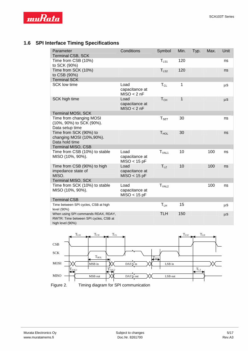
1.6 SPI Interface Timing Specifications
Parameter Conditions Symbol Min. Typ. Max. Unit
Terminal CSB, SCK Time from CSB (10%) to SCK (90%)
TLS1 120 ns
Time from SCK (10%) to CSB (90%)
TLS2 120 ns
Terminal SCK SCK low time Load
capacitance at MISO < 2 nF
TCL 1 s
SCK high time Load capacitance at MISO < 2 nF
TCH 1 s
Terminal MOSI, SCK Time from changing MOSI (10%, 90%) to SCK (90%). Data setup time
TSET 30 ns
Time from SCK (90%) to changing MOSI (10%,90%). Data hold time
THOL 30 ns
Terminal MISO, CSB Time from CSB (10%) to stable MISO (10%, 90%).
Load capacitance at MISO < 15 pF
TVAL1 10 100 ns
Time from CSB (90%) to high impedance state of MISO.
Load capacitance at MISO < 15 pF
TLZ 10 100 ns
Terminal MISO, SCK Time from SCK (10%) to stable MISO (10%, 90%).
Load capacitance at MISO < 15 pF
TVAL2 100 ns
Terminal CSB Time between SPI cycles, CSB at high
level (90%)
TLH 15 s
When using SPI commands RDAX, RDAY,
RWTR: Time between SPI cycles, CSB at
high level (90%)
TLH 150 s
Figure 2. Timing diagram for SPI communication

SCA103T Series
Murata Electronics Oy Subject to changes 6/17
www.muratamems.fi Doc.Nr. 8261700 Rev.A3
1.7 Electrical Connection
If the SPI interface is not used SCK (pin1), MISO (pin3), MOSI (pin4) and CSB (pin7) must be left floating. Self-test can be activated applying logic “1” (positive supply voltage level) to ST_1 or ST_2 pins (pins 10 or 9). Self-test must not be activated for both channels at the same time. If the ST feature is not used, pins 9 and 10 must be left floating or connected to GND. Inclination signals are provided from pins OUT_1 and OUT_2.
1
2
3
4
5
6 7
8
9
10
11
12SCK
Ext_C_1
MISO
MOSI
OUT_2
VSS CSB
Ext_C_2
ST_2
ST_1/Test_in
OUT_1
VDD
Figure 3. SCA103T electrical connection
No. Node I/O Description 1 SCK Input Serial clock 2 NC Input No connect, left floating 3 MISO Output Master in slave out; data output 4 MOSI Input Master out slave in; data input 5 Out_2 Output Output 2 (Ch 2) 6 GND Supply Ground 7 CSB Input Chip select (active low) 8 NC Input No connect, left floating 9 ST_2 Input Self test input for Ch 2
10 ST_1 Input Self test input for Ch 1 11 Out_1 Output Output 1(Ch 1) 12 VDD Supply Positive supply voltage (+5V DC)
1.8 Typical Performance Characteristics
Typical offset and sensitivity temperature dependencies of SCA103T are presented in following diagrams. These results represent the typical performance of SCA103T components. The mean
value and 3 sigma limits (mean ± 3 standard deviation) and specification limits are presented in following diagrams. The 3 sigma limits represents 99.73% of the SCA103T population.
SCK
MISO
MOSI
OUT_2
GND
VDD
OUT_1
ST_1
ST_2
CSB

SCA103T Series
Murata Electronics Oy Subject to changes 7/17
www.muratamems.fi Doc.Nr. 8261700 Rev.A3
031.0*0032.0*00005.0*0000005.0 23 TTTScorr
temperature dependency of SCA103T offset (differential output)
-0.3
-0.2
-0.1
0
0.1
0.2
0.3
-40 -20 0 20 40 60 80 100 120
Temp [°C]
Dif
fere
nti
al o
ffset
err
or
[deg
rees]
average
+3 Sigma
-3 Sigma
specif ication limit
specif ication limit
Temperature dependency of SCA103T sensitivity [%] (differential output)
-3
-2.5
-2
-1.5
-1
-0.5
0
0.5
1
1.5
-40 -20 0 20 40 60 80 100 120
Temp [°C]
Dif
fere
nti
al sen
sit
ivit
y e
rro
r [%
]
average
+3 Sigma
-3 Sigma
specif ication
limit
specif ication
limit
Figure 4. Typical temperature dependency of SCA103T offset
Figure 5. Typical temperature dependency of SCA103T sensitivity
1.8.1 Additional External Compensation
To achieve the best possible accuracy, the temperature measurement information and typical temperature dependency curve can be used for SCA103T sensitivity temperature dependency compensation. The offset temperature dependency curves do not have any significant tendency so there is no need for any additional external compensation for offset.
By using an additional 3rd order polynome compensation curve based on average sensitivity temperature dependency curve and temperature measurement information, it is possible to reduce sensitivity temperature dependency from 0.013%/°C down to 0.005%/°C.
The equation for the fitted 3
rd order polynome curve is:
Where:
Scorr: 3rd
order polynome fitted to average sensitivity temperature dependency curve T temperature in °C (Refer to paragraph 2.7- Temperature Measurement)

SCA103T Series
Murata Electronics Oy Subject to changes 8/17
www.muratamems.fi Doc.Nr. 8261700 Rev.A3
)100/1(* ScorrSENSSENScomp
The temperature dependency of 3rd order compensated SCA103T sensitivity [%]
(differential output)
-1
-0.8
-0.6
-0.4
-0.2
0
0.2
0.4
0.6
0.8
1
-40 -20 0 20 40 60 80
Temp [°C]
Dif
fere
nti
al sen
sit
ivit
y e
rro
r [%
]
compensated
average+3 Sigma limit
-3 Sigma limit
The calculated compensation curve can be used to compensate for the temperature dependency of the SCA103T sensitivity by using following equation: Where:
SENScomp temperature compensated sensitivity SENS Nominal sensitivity (16V/g SCA103T-D04, 8V/g SCA103T-D05)
The typical sensitivity temperature dependency after 3rd order compensation is shown in the figure below. Figure 6. The temperature dependency of 3
rd order compensated SCA103T sensitivity
2 Functional Description
2.1 Differential Measurement
The measuring axis of SCA103T sensing elements are mutually opposite in direction, thus providing two inclination signals which can be differentiated externally, either by using a differential amplifier or a microcontroller. The differential measurement principle removes all common mode measurement errors. Most of the error sources have similar effects on both sensing elements. These errors are removed from measurement result during signal differentiation. The differential measurement principle gives very efficient noise reduction, improved long term stability and extremely low temperature dependency.
SCA103T Series
Murata Electronics Oy Subject to changes 9/17
www.muratamems.fi Doc.Nr. 8261700 Rev.A3
SCA103T-D04 outputs and differential amplifier output
-6.0
-5.0
-4.0
-3.0
-2.0
-1.0
0.0
1.0
2.0
3.0
4.0
5.0
6.0
-20 -15 -10 -5 0 5 10 15 20
Tilt angle [ ° ]
Ou
tpu
t [V
] SCA103T OUT_1
SCA103T OUT_2
Differential output
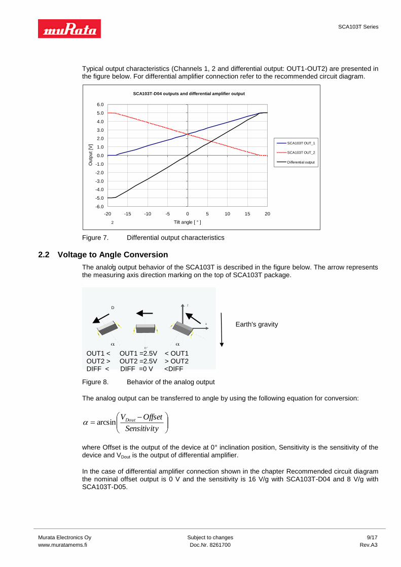
Typical output characteristics (Channels 1, 2 and differential output: OUT1-OUT2) are presented in the figure below. For differential amplifier connection refer to the recommended circuit diagram.
Figure 7. Differential output characteristics
2.2 Voltage to Angle Conversion
The analog output behavior of the SCA103T is described in the figure below. The arrow represents the measuring axis direction marking on the top of SCA103T package.
Figure 8. Behavior of the analog output
The analog output can be transferred to angle by using the following equation for conversion:
ySensitivit
OffsetVDoutarcsin
where Offset is the output of the device at 0° inclination position, Sensitivity is the sensitivity of the device and VDout is the output of differential amplifier.
In the case of differential amplifier connection shown in the chapter Recommended circuit diagram the nominal offset output is 0 V and the sensitivity is 16 V/g with SCA103T-D04 and 8 V/g with SCA103T-D05.
OUT1 < OUT1 =2.5V < OUT1 OUT2 > OUT2 =2.5V > OUT2 DIFF < DIFF =0 V <DIFF
Earth's gravity
2
1
D
SCA103T Series
Murata Electronics Oy Subject to changes 10/17
www.muratamems.fi Doc.Nr. 8261700 Rev.A3
ySensitivit
OffsetVDout
Angles close to 0° inclination can be estimated quite accurately with straight line conversion but for best possible accuracy arcsine conversion is recommended to be used. Following table shows the angle measurement error if straight line conversion is used. Straight line conversion equation:
Where: Sensitivity = 280mV/° with SCA103T-D04 or Sensitivity= 140mV/° with SCA103T-D05
Tilt angle [°] Straight line conversion error [°]
0 0 1 0.0027 2 0.0058 3 0.0094 4 0.0140 5 0.0198 10 0.0787 15 0.2185 30 1.668
2.3 Ratiometric Output
Ratiometric output means that the zero offset point and sensitivity of the sensor are proportional to the supply voltage. If the SCA103T supply voltage is fluctuating, the SCA103T output will also vary. When the same reference voltage for both the SCA103T sensor and the measuring part (A/D-converter) is used, the error caused by reference voltage variation is automatically compensated.
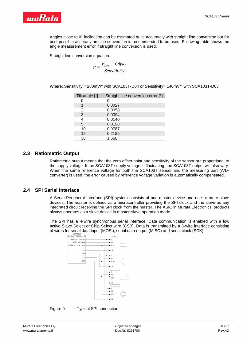
2.4 SPI Serial Interface
A Serial Peripheral Interface (SPI) system consists of one master device and one or more slave devices. The master is defined as a microcontroller providing the SPI clock and the slave as any integrated circuit receiving the SPI clock from the master. The ASIC in Murata Electronics’ products always operates as a slave device in master-slave operation mode. The SPI has a 4-wire synchronous serial interface. Data communication is enabled with a low active Slave Select or Chip Select wire (CSB). Data is transmitted by a 3-wire interface consisting of wires for serial data input (MOSI), serial data output (MISO) and serial clock (SCK).
DATA OUT (MOSI)
DATA IN (MISO)
SERIAL CLOCK (SCK)
SS0
SS1
SS2
SS3
MASTER
MICROCONTROLLER
SI
SO
SCK
CS
SLAVE
SI
SO
SCK
CS
SI
SO
SCK
CS
SI
SO
SCK
CS
Figure 9. Typical SPI connection
SCA103T Series
Murata Electronics Oy Subject to changes 11/17
www.muratamems.fi Doc.Nr. 8261700 Rev.A3
The SPI interface in Murata products is designed to support any micro controller that uses SPI bus. Communication can be carried out by software or hardware based SPI. Please note that in the case of hardware based SPI, the received acceleration data is 11 bits. The data transfer uses the following 4-wire interface:
MOSI master out slave in µP → SCA103T MISO master in slave out SCA103T → µP SCK serial clock µP → SCA103T CSB chip select (low active) µP → SCA103T
Each transmission starts with a falling edge of CSB and ends with the rising edge. During transmission, commands and data are controlled by SCK and CSB according to the following rules:
commands and data are shifted; MSB first, LSB last
each output data/status bits are shifted out on the falling edge of SCK (MISO line)
each bit is sampled on the rising edge of SCK (MOSI line)
after the device is selected with the falling edge of CSB, an 8-bit command is received. The command defines the operations to be performed
the rising edge of CSB ends all data transfer and resets internal counter and command register
if an invalid command is received, no data is shifted into the chip and the MISO remains in high impedance state until the falling edge of CSB. This reinitializes the serial communication.
data transfer to MOSI continues immediately after receiving the command in all cases where data is to be written to SCA103T’s internal registers
data transfer out from MISO starts with the falling edge of SCK immediately after the last bit of the SPI command is sampled in on the rising edge of SCK
maximum SPI clock frequency is 500kHz
maximum data transfer speed for RDAX and RDAY is 5300 samples per sec / channel
SPI command can be either an individual command or a combination of command and data. In the case of combined command and data, the input data follows uninterruptedly the SPI command and the output data is shifted out in parallel with the input data. The SPI interface uses an 8-bit instruction (or command) register. The list of commands is given in Table below.
Command name
Command format
Description:
MEAS 00000000 Measure mode (normal operation mode after power on) RWTR 00001000 Read temperature data register STX 00001110 Activate Self test for X-channel STY 00001111 Activate Self test for Y-channel RDAX 00010000 Read X-channel acceleration RDAY 00010001 Read Y-channel acceleration
Measure mode (MEAS) is the standard operation mode after power-up. During normal operation, MEAS command is the exit command from Self test. Read temperature data register (RWTR) reads the temperature data register during normal operation without effecting the operation. Temperature data register is updated every 150 µs. The load operation is disabled whenever the CSB signal is low, hence CSB must stay high at least 150 µs prior to the RWTR command in order to guarantee correct data. The data transfer is presented in figure 10 below. The data is transferred MSB first. In normal operation, it does not matter what data is written into temperature data register during the RWTR command and hence writing all zeros is recommended.

SCA103T Series
Murata Electronics Oy Subject to changes 12/17
www.muratamems.fi Doc.Nr. 8261700 Rev.A3
Figure 10. Command and 8 bit temperature data transmission over the SPI
Self test for X-channel (STX) activates the self test function for the X-channel (Channel 1). The internal charge pump is activated and a high voltage is applied to the X-channel acceleration sensor element electrode. This causes the electrostatic force that deflects the beam of the sensing element and simulates the acceleration to the positive direction. The self-test is de-activated by giving the MEAS command. The self test function must not be activated for both channels at the same time. Self test for Y-channel (STY) activates the self test function for the Y-channel (Channel 2). The internal charge pump is activated and a high voltage is applied to the Y-channel acceleration sensor element electrode. Read X-channel acceleration (RDAX) accesses the AD converted X-channel (Channel 1) acceleration signal stored in acceleration data register X. Read Y-channel acceleration (RDAY) accesses the AD converted Y-channel (Channel 2) acceleration signal stored in acceleration data register Y. During normal operation, acceleration data registers are reloaded every 150 µs. The load operation is disabled whenever the CSB signal is low, hence CSB must stay high at least 150 µs prior to the RDAX command in order to guarantee correct data. Data output is an 11-bit digital word that is fed out MSB first and LSB last.
Figure 11. Command and 11 bit acceleration data transmission over the SPI
2.5 Digital Output to Angle Conversion
The acceleration measurement results in RDAX and RDAY data registers are in 11 bit digital word format. The data range is from 0 to 2048. The nominal content of RDAX and RDAY data registers in zero angle position are: Binary: 100 0000 0000 Decimal: 1024

SCA103T Series
Murata Electronics Oy Subject to changes 13/17
www.muratamems.fi Doc.Nr. 8261700 Rev.A3
To obtain the differential digital output value, Dout, RDAY must be subtracted from RDAX.
Dout = RDAX – RDAY
The transfer function from differential digital output to angle can be presented as
LSB/g
LSBLSBarcsin
0@
Sens
DD outout
where;
Dout differential digital output (RDAX – RDAY) Dout@0° digital offset value, nominal value = 0 in differential mode
angle Sens sensitivity of the device. (SCA103T-D04: 6554, SCA103T-D05: 3277)
As an example, the following table contains SCA103T-D04 data register values and calculated differential digital output values with -5, -1 0, 1 and 5 degree tilt angles.
Angle [°]
Acceleration [mg]
RDAX RDAY DOUT (RDAX–RDAY)
-5 -87.16 dec: 739 bin: 010 1110 0011
dec: 1309 bin: 101 0001 1101
dec: -570
-1 -17.45 dec: 967 bin: 011 1100 0111
dec: 1081 bin: 100 0011 1001
dec: -144
0 0 dec: 1024 bin: 100 0000 0000
dec: 1024 bin: 100 0000 0000
dec: 0
1 17.45 dec: 1081 bin: 100 0011 1001
dec: 967 bin: 011 1100 0111
dec: 114
5 87.16 dec: 1309 bin: 101 0001 1101
dec: 739 bin: 010 1110 0011
dec: 570
2.6 Self Test and Failure Detection Modes
To ensure reliable measurement results, the SCA103T has continuous interconnection failure and calibration memory validity detection. A detected failure forces the output signal close to power supply ground or VDD level, outside the normal output range. The normal output ranges are: analog 0.25-4.75 V (@Vdd=5V) and SPI 102...1945 counts. The calibration memory validity is verified by continuously running parity checks for the control register memory content. In a case where a parity error is detected the control register is automatically re-loaded from the EEPROM. If a new parity error is detected after re-loading data both analog output voltages are forced to go close to ground level (<0.25 V) and SPI outputs goes below 102 counts. The SCA103T also includes a separate self test mode. The true self test simulates acceleration, or deceleration, using an electrostatic force. The electrostatic force simulates acceleration that is high enough to deflect the proof mass to its extreme positive position, and this causes the output signal to go to the maximum value. The self test function is activated either by a separate on-off command on the self test input, or through the SPI. The self-test generates an electrostatic force, deflecting the sensing element’s proof mass, thus checking the complete signal path. The true self test performs following checks:
Sensing element movement check
ASIC signal path check
PCB signal path check

SCA103T Series
Murata Electronics Oy Subject to changes 14/17
www.muratamems.fi Doc.Nr. 8261700 Rev.A3
083.1
197
CountsT
Micro controller A/D and signal path check The created deflection can be seen both in the SPI and analogue output. The self test function is activated digitally by a STX or STY command, and de-activated by a MEAS command. Self test can be also activated applying logic”1” (positive supply voltage level) to ST pins (pins 9 & 10) of SCA103T. The self test Input high voltage level is 4 – Vdd+0.3 V and input low voltage level is 0.3 – 1 V. The self test function must not be activated for both channels at the same time.
Figure 12. Self test wave forms Self test characteristics:
T1 [ms] T2 [ms] T3 [ms] T4 [ms] T5 [ms] V2: V3:
20-100 Typ. 25 Typ. 30 Typ. 55 Typ. 15 Min 0.95*VDD (4.75V @Vdd=5V)
0.95*V1-1.05*V1
V1 = initial output voltage before the self test function is activated. V2 = output voltage during the self test function. V3 = output voltage after the self test function has been de-activated and after stabilization time Please note that the error band specified for V3 is to guarantee that the output is within 5% of the initial value after the specified stabilization time. After a longer time (max. 1 second) V1=V3. T1 = Pulse length for Self test activation T2 = Saturation delay T3 = Recovery time T4 = Stabilization time =T2+T3 T5 = Rise time during self test
2.7 Temperature Measurement
The SCA103T has an internal temperature sensor, which is used for internal offset compensation. The temperature information is also available for additional external compensation. The temperature sensor can be accessed via the SPI interface and the temperature reading is an 8-bit word (0…255). The transfer function is expressed by the following formula: Where:
Counts Temperature reading T Temperature in °C
The temperature measurement output is not calibrated. The internal temperature compensation routine uses relative results where absolute accuracy is not needed. If the temperature measurement results are used for additional external compensation then one point calibration in the system level is needed to remove the offset. With external one point calibration the accuracy of the temperature measurement is about ±1 °C.
Vout
5V
0 V
T5
T1 T2 T3
T4
V1 V2 V3
ST pin voltage
0 V
5 V
SCA103T Series
Murata Electronics Oy Subject to changes 15/17
www.muratamems.fi Doc.Nr. 8261700 Rev.A3
3 Application Information
3.1 Recommended Circuit Diagrams and Printed Circuit Board Layouts
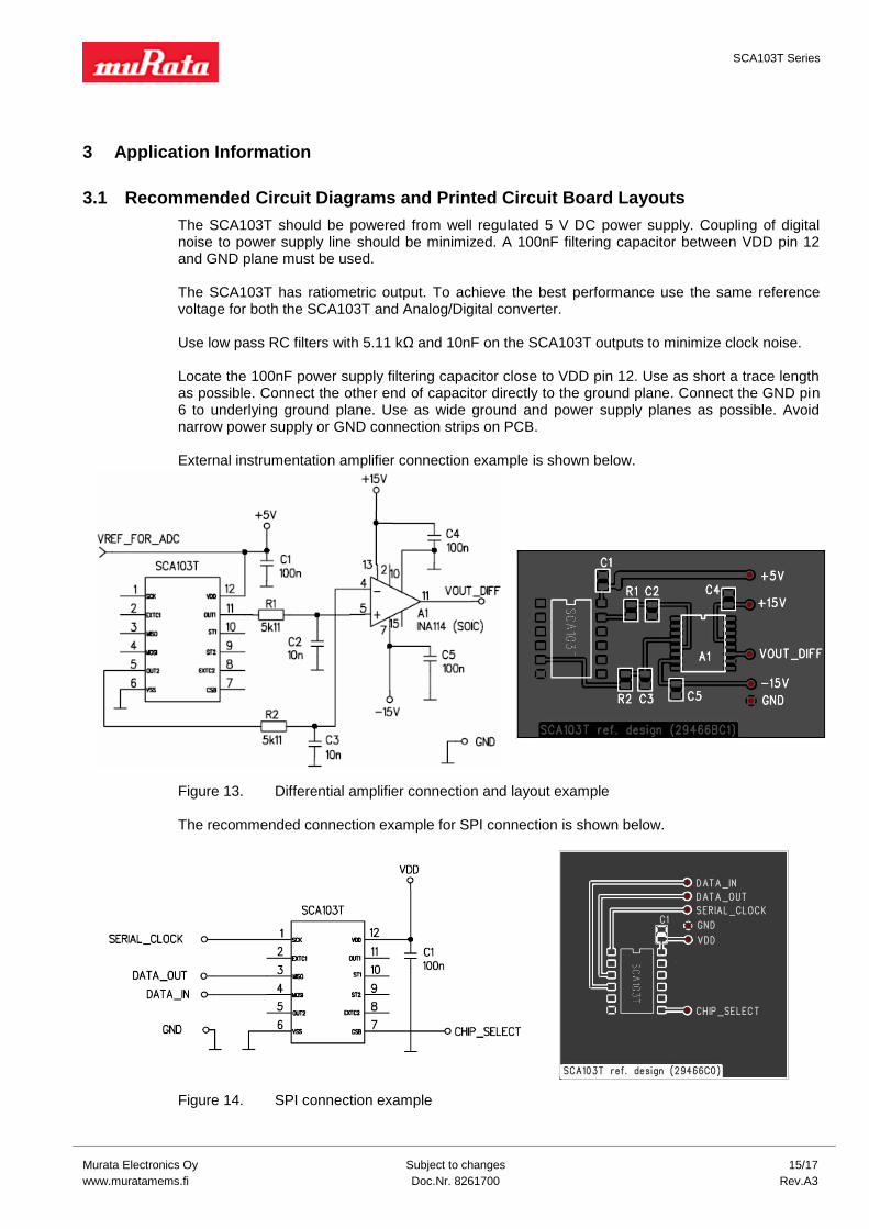
The SCA103T should be powered from well regulated 5 V DC power supply. Coupling of digital noise to power supply line should be minimized. A 100nF filtering capacitor between VDD pin 12 and GND plane must be used. The SCA103T has ratiometric output. To achieve the best performance use the same reference voltage for both the SCA103T and Analog/Digital converter. Use low pass RC filters with 5.11 kΩ and 10nF on the SCA103T outputs to minimize clock noise. Locate the 100nF power supply filtering capacitor close to VDD pin 12. Use as short a trace length as possible. Connect the other end of capacitor directly to the ground plane. Connect the GND pin 6 to underlying ground plane. Use as wide ground and power supply planes as possible. Avoid narrow power supply or GND connection strips on PCB. External instrumentation amplifier connection example is shown below.
Figure 13. Differential amplifier connection and layout example
The recommended connection example for SPI connection is shown below.
Figure 14. SPI connection example

SCA103T Series
Murata Electronics Oy Subject to changes 16/17
www.muratamems.fi Doc.Nr. 8261700 Rev.A3
3.2 Recommended Printed Circuit Board Footprint
Figure 15. Recommended PCB footprint
4 Mechanical Specifications and Reflow Soldering
4.1 Mechanical Specifications (Reference only)
Lead frame material: Copper Plating: Nickel followed by Gold Solderability: JEDEC standard: JESD22-B102-C RoHS compliance: RoHS compliant lead-free component. Co-planarity error 0.1mm max. The part weights <1.2 g
Figure 16. Mechanical dimensions of the SCA103T. (Dimensions in mm)

SCA103T Series
Murata Electronics Oy Subject to changes 17/17
www.muratamems.fi Doc.Nr. 8261700 Rev.A3
4.2 Reflow Soldering
The SCA103T is suitable for Sn-Pb eutectic and Pb-free soldering process and mounting with normal SMD pick-and-place equipment.
Figure 17. Recommended SCA103T body temperature profile during reflow soldering. Ref.
IPC/JEDEC J-STD-020B.
Profile feature Sn-Pb Eutectic Assembly
Pb-free Assembly
Average ramp-up rate (TL to TP) 3°C/second max. 3°C/second max.
Preheat
- Temperature min (Tsmin)
- Temperature max (Tsmax)
- Time (min to max) (ts)
100°C
150°C
60-120 seconds
150°C
200°C
60-180 seconds
Tsmax to T, Ramp up rate 3°C/second max
Time maintained above:
- Temperature (TL)
- Time (tL)
183°C
60-150 seconds
217°C
60-150 seconds
Peak temperature (TP) 240 +0/-5°C 250 +0/-5°C
Time within 5°C of actual Peak Temperature (TP) 10-30 seconds 20-40 seconds
Ramp-down rate 6°C/second max 6°C/second max
Time 25° to Peak temperature 6 minutes max 8 minutes max
The Moisture Sensitivity Level of the part is 3 according to the IPC/JEDEC J-STD-020B. The part should be delivered in a dry pack. The manufacturing floor time (out of bag) in the customer’s end is 168 hours.
Notes: Preheating time and temperatures according to solder paste manufacturer.
It is important that the part is parallel to the PCB plane and that there is no angular alignment error from intended measuring direction during the assembly process.
Wave soldering is not recommended.
Ultrasonic cleaning is not allowed. The sensing element may be damaged by an ultrasonic cleaning process.