the reconfigurable cluster element reconfigurable cluster element document version: ... 1.2 the...
TRANSCRIPT
Detector R & D
DAQ Building Blocks Modular building blocks for massivally scaled DAQ systems
The Reconfigurable Cluster Element
Document Version: 0.1 Document Issue: 0 Document Edition: English Document Status: Draft - for internal distribution only Document ID: To be assigned Document Date: February 26, 2010
National Accelerator Laboratory 2575 Sandhill Road
Menlo Park California, 94025 USA
DAQ Building Blocks The Reconfigurable Cluster Element February 26, 2010 Version/Issue: 0.1/0
page 2 Draft - for internal distribution only
This document has been prepared using the Software Documentation Layout Templates that have been prepared by the IPT Group (Information, Process and Technology), IT Division, CERN (The European Laboratory for Particle Physics). For more information, go to http://framemaker.cern.ch/.
DAQ Building Blocks The Reconfigurable Cluster Element Abstract Version/Issue: 0.1/0
Abstract
To be written.
Hardware compatibility
This document assumes the following hardware revisions: TBD.
Intended audience
TBW.
Conventions used in this document
Certain special typographical conventions are used in this document. They are documented here for the convenience of the reader:
• Field names are shown in bold and italics (e.g., respond or parity).
• Acronyms are shown in small caps (e.g., SLAC or CDS).
• Hardware signal or register names are shown in Courier bold (e.g., RIGHT_FIRST or LAYER_MASK_1)
Draft - for internal distribution only page 3
DAQ Building Blocks The Reconfigurable Cluster Element References Version/Issue: 0.1/0
References
1 Preliminary Product Specification of the Xilinx Virtex-4 Family Overview, dated June 17, 2005
2 Infiniband Architecture Specification Volume 1, Release 1.2. Dated October 2004 (final release).
3 Xilinix Virtex-4 Family Overview, Preliminary Product specification, dated February 10, 2006
page 4 Draft - for internal distribution only
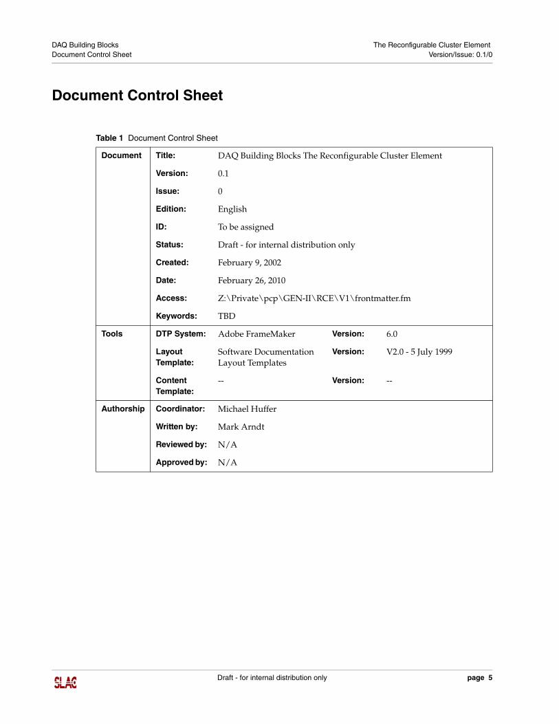
DAQ Building Blocks The Reconfigurable Cluster Element Document Control Sheet Version/Issue: 0.1/0
Document Control Sheet
Table 1 Document Control Sheet
Document Title: DAQ Building Blocks The Reconfigurable Cluster Element
Version: 0.1
Issue: 0
Edition: English
ID: To be assigned
Status: Draft - for internal distribution only
Created: February 9, 2002
Date: February 26, 2010
Access: Z:\Private\pcp\GEN-II\RCE\V1\frontmatter.fm
Keywords: TBD
Tools DTP System: Adobe FrameMaker Version: 6.0
Layout Template:
Software Documentation Layout Templates
Version: V2.0 - 5 July 1999
Content Template:
-- Version: --
Authorship Coordinator: Michael Huffer
Written by: Mark Arndt
Reviewed by: N/A
Approved by: N/A
Draft - for internal distribution only page 5
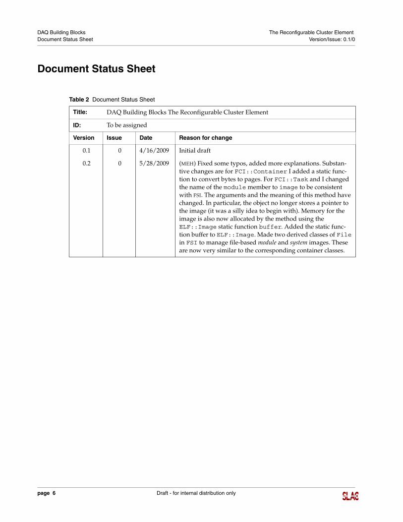
DAQ Building Blocks The Reconfigurable Cluster Element Document Status Sheet Version/Issue: 0.1/0
Document Status Sheet
Table 2 Document Status Sheet
Title: DAQ Building Blocks The Reconfigurable Cluster Element
ID: To be assigned
Version Issue Date Reason for change
0.1 0 4/16/2009 Initial draft
0.2 0 5/28/2009 (MEH) Fixed some typos, added more explanations. Substan-tive changes are for FCI::Container I added a static func-tion to convert bytes to pages. For FCI::Task and I changed the name of the module member to image to be consistent with FSI. The arguments and the meaning of this method have changed. In particular, the object no longer stores a pointer to the image (it was a silly idea to begin with). Memory for the image is also now allocated by the method using the ELF::Image static function buffer. Added the static func-tion buffer to ELF::Image. Made two derived classes of File in FSI to manage file-based module and system images. These are now very similar to the corresponding container classes.
page 6 Draft - for internal distribution only
DAQ Building Blocks The Reconfigurable Cluster Element Table of Contents Version/Issue: 0.1/0
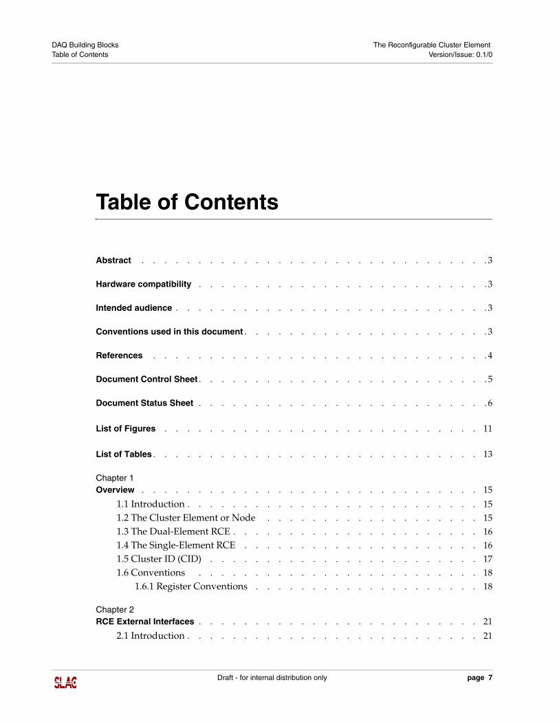
Table of Contents
Abstract . . . . . . . . . . . . . . . . . . . . . . . . . . . . . . . 3
Hardware compatibility . . . . . . . . . . . . . . . . . . . . . . . . . . 3
Intended audience . . . . . . . . . . . . . . . . . . . . . . . . . . . . 3
Conventions used in this document . . . . . . . . . . . . . . . . . . . . . . 3
References . . . . . . . . . . . . . . . . . . . . . . . . . . . . . . 4
Document Control Sheet . . . . . . . . . . . . . . . . . . . . . . . . . . 5
Document Status Sheet . . . . . . . . . . . . . . . . . . . . . . . . . . 6 List of Figures . . . . . . . . . . . . . . . . . . . . . . . . . . . . 11 List of Tables . . . . . . . . . . . . . . . . . . . . . . . . . . . . . 13
Chapter 1 Overview . . . . . . . . . . . . . . . . . . . . . . . . . . . . . . 15
1.1 Introduction . . . . . . . . . . . . . . . . . . . . . . . . . . 151.2 The Cluster Element or Node . . . . . . . . . . . . . . . . . . . 151.3 The Dual-Element RCE . . . . . . . . . . . . . . . . . . . . . . 161.4 The Single-Element RCE . . . . . . . . . . . . . . . . . . . . . 161.5 Cluster ID (CID) . . . . . . . . . . . . . . . . . . . . . . . . 171.6 Conventions . . . . . . . . . . . . . . . . . . . . . . . . . 18
1.6.1 Register Conventions . . . . . . . . . . . . . . . . . . . . 18
Chapter 2 RCE External Interfaces . . . . . . . . . . . . . . . . . . . . . . . . . 21
2.1 Introduction . . . . . . . . . . . . . . . . . . . . . . . . . . 21
Draft - for internal distribution only page 7
DAQ Building Blocks The Reconfigurable Cluster Element Table of Contents Version/Issue: 0.1/0
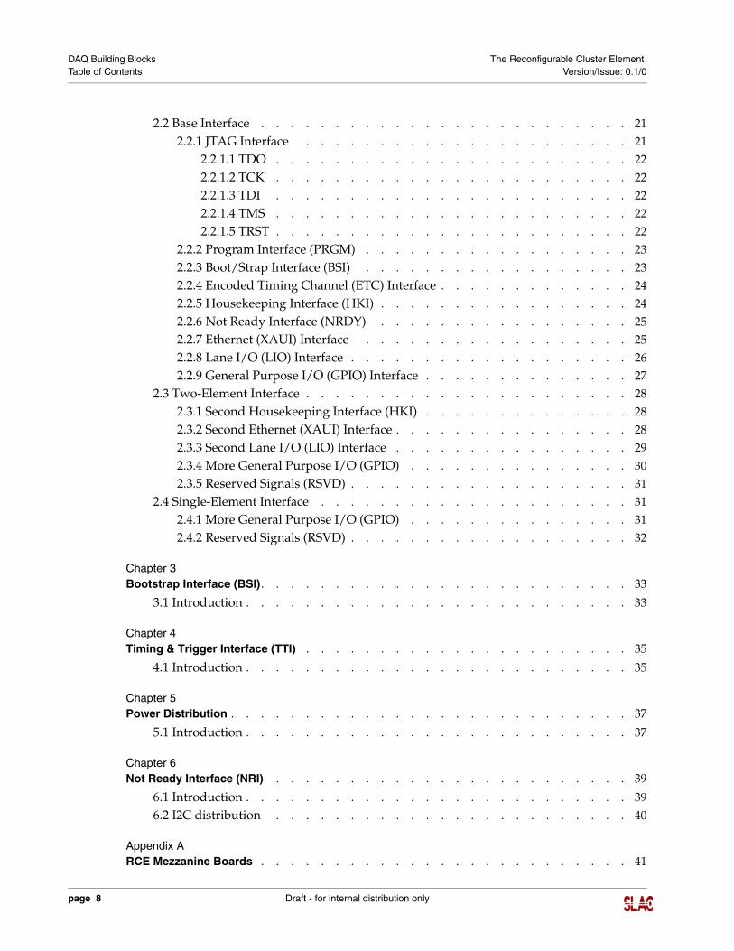
2.2 Base Interface . . . . . . . . . . . . . . . . . . . . . . . . . 212.2.1 JTAG Interface . . . . . . . . . . . . . . . . . . . . . . 21
2.2.1.1 TDO . . . . . . . . . . . . . . . . . . . . . . . . 222.2.1.2 TCK . . . . . . . . . . . . . . . . . . . . . . . . 222.2.1.3 TDI . . . . . . . . . . . . . . . . . . . . . . . . 222.2.1.4 TMS . . . . . . . . . . . . . . . . . . . . . . . . 222.2.1.5 TRST . . . . . . . . . . . . . . . . . . . . . . . . 22
2.2.2 Program Interface (PRGM) . . . . . . . . . . . . . . . . . . 232.2.3 Boot/Strap Interface (BSI) . . . . . . . . . . . . . . . . . . 232.2.4 Encoded Timing Channel (ETC) Interface . . . . . . . . . . . . . 242.2.5 Housekeeping Interface (HKI) . . . . . . . . . . . . . . . . . 242.2.6 Not Ready Interface (NRDY) . . . . . . . . . . . . . . . . . 252.2.7 Ethernet (XAUI) Interface . . . . . . . . . . . . . . . . . . 252.2.8 Lane I/O (LIO) Interface . . . . . . . . . . . . . . . . . . . 262.2.9 General Purpose I/O (GPIO) Interface . . . . . . . . . . . . . . 27
2.3 Two-Element Interface . . . . . . . . . . . . . . . . . . . . . . 282.3.1 Second Housekeeping Interface (HKI) . . . . . . . . . . . . . . 282.3.2 Second Ethernet (XAUI) Interface . . . . . . . . . . . . . . . . 282.3.3 Second Lane I/O (LIO) Interface . . . . . . . . . . . . . . . . 292.3.4 More General Purpose I/O (GPIO) . . . . . . . . . . . . . . . 302.3.5 Reserved Signals (RSVD) . . . . . . . . . . . . . . . . . . . 31
2.4 Single-Element Interface . . . . . . . . . . . . . . . . . . . . . 312.4.1 More General Purpose I/O (GPIO) . . . . . . . . . . . . . . . 312.4.2 Reserved Signals (RSVD) . . . . . . . . . . . . . . . . . . . 32
Chapter 3 Bootstrap Interface (BSI). . . . . . . . . . . . . . . . . . . . . . . . . 33
3.1 Introduction . . . . . . . . . . . . . . . . . . . . . . . . . . 33
Chapter 4 Timing & Trigger Interface (TTI) . . . . . . . . . . . . . . . . . . . . . . 35
4.1 Introduction . . . . . . . . . . . . . . . . . . . . . . . . . . 35
Chapter 5 Power Distribution . . . . . . . . . . . . . . . . . . . . . . . . . . . 37
5.1 Introduction . . . . . . . . . . . . . . . . . . . . . . . . . . 37
Chapter 6 Not Ready Interface (NRI) . . . . . . . . . . . . . . . . . . . . . . . . 39
6.1 Introduction . . . . . . . . . . . . . . . . . . . . . . . . . . 396.2 I2C distribution . . . . . . . . . . . . . . . . . . . . . . . . 40
Appendix A RCE Mezzanine Boards . . . . . . . . . . . . . . . . . . . . . . . . . 41
page 8 Draft - for internal distribution only
DAQ Building Blocks The Reconfigurable Cluster Element Table of Contents Version/Issue: 0.1/0
A.1 Introduction . . . . . . . . . . . . . . . . . . . . . . . . . 41A.1.1 Connector numerology . . . . . . . . . . . . . . . . . . . 41A.1.2 Dual-Element board . . . . . . . . . . . . . . . . . . . . 42
A.1.2.1 Bill of Materials . . . . . . . . . . . . . . . . . . . . 43A.1.3 Single-Element board . . . . . . . . . . . . . . . . . . . . 44
A.2 The Power Connectors . . . . . . . . . . . . . . . . . . . . . . 45A.3 The A-Signal connectors . . . . . . . . . . . . . . . . . . . . . 46
A.3.4 A-Receive Connector pin-outs . . . . . . . . . . . . . . . . . 47A.3.4.2 Row-1 . . . . . . . . . . . . . . . . . . . . . . . 47A.3.4.3 Row-2 . . . . . . . . . . . . . . . . . . . . . . . 48
A.3.5 A-Transmit Connector pin-outs . . . . . . . . . . . . . . . . 49A.3.5.4 Row-1 . . . . . . . . . . . . . . . . . . . . . . . 49A.3.5.5 Row-2 . . . . . . . . . . . . . . . . . . . . . . . 50
A.4 The Connectors for the Dual-Element board . . . . . . . . . . . . . . 51A.4.6 B-Receive Connector pin-outs . . . . . . . . . . . . . . . . . 52
A.4.6.6 Row-1 . . . . . . . . . . . . . . . . . . . . . . . 52A.4.6.7 Row-2 . . . . . . . . . . . . . . . . . . . . . . . 53
A.4.7 B-Transmit Connector pin-outs . . . . . . . . . . . . . . . . 54A.4.7.8 Row-1 . . . . . . . . . . . . . . . . . . . . . . . 54A.4.7.9 Row-2 . . . . . . . . . . . . . . . . . . . . . . . 55
A.5 The Connectors for the Single-Element board . . . . . . . . . . . . . 56A.5.8 B-Receive Connector pin-outs . . . . . . . . . . . . . . . . . 58
A.5.8.10 Row-1 . . . . . . . . . . . . . . . . . . . . . . . 58A.5.8.11 Row-2 . . . . . . . . . . . . . . . . . . . . . . . 59
A.5.9 B-Transmit Connector pin-outs . . . . . . . . . . . . . . . . 60A.5.9.12 Row-1 . . . . . . . . . . . . . . . . . . . . . . . 60A.5.9.13 Row-2 . . . . . . . . . . . . . . . . . . . . . . . 61
Appendix B Gen I Mezzanine Board . . . . . . . . . . . . . . . . . . . . . . . . . 63
B.1 Board . . . . . . . . . . . . . . . . . . . . . . . . . . . . 63
Draft - for internal distribution only page 9

DAQ Building Blocks The Reconfigurable Cluster Element Table of Contents Version/Issue: 0.1/0
page 10 Draft - for internal distribution only
DAQ Building Blocks The Reconfigurable Cluster Element List of Figures Version/Issue: 0.1/0
List of Figures
Figure 1 p. 15 Block diagram of the Cluster Element or Node
Figure 2 p. 16 Block diagram of the Dual-Element RCE
Figure 3 p. 17 Block diagram of the Single-Element RCE
Figure 4 p. 34 Block diagram of the Bootstrap Interface
Figure 5 p. 36 Timing & Trigger Interface
Figure 6 p. 38 Block diagram of power distribution
Figure 7 p. 40 I2C distribution within a cluster
Figure A.1 p. 42 Mezzanine board connector naming conventions
Figure A.2 p. 42 Dual-Element Mezzanine board (component side)
Figure A.3 p. 43 Dual-Element Mezzanine board (connector side)
Figure A.4 p. 44 Single-Element Mezzanine board (component side)
Figure A.5 p. 45 Single-Element Mezzanine board (connector side)
Figure A.6 p. 45 Mapping of power and ground to a Power Connector
Figure A.7 p. 46 Mapping of interface signals to the A-Signal connectors
Figure A.8 p. 51 Mapping of the interface signals to the Dual-Element Connectors
Figure A.9 p. 57 Mapping of the interface signals to the Single-Element Connectors
Figure B.1 p. 63 Single-Element (GEN-I) Mezzanine board (component side)
Figure B.2 p. 64 Single -Element (GEN-I) Mezzanine board (connector side)
Draft - for internal distribution only page 11
DAQ Building Blocks The Reconfigurable Cluster Element List of Figures Version/Issue: 0.1/0
page 12 Draft - for internal distribution only
DAQ Building Blocks The Reconfigurable Cluster Element List of Tables Version/Issue: 0.1/0
List of Tables
Table 1 p. 5 Document Control Sheet
Table 2 p. 6 Document Status Sheet
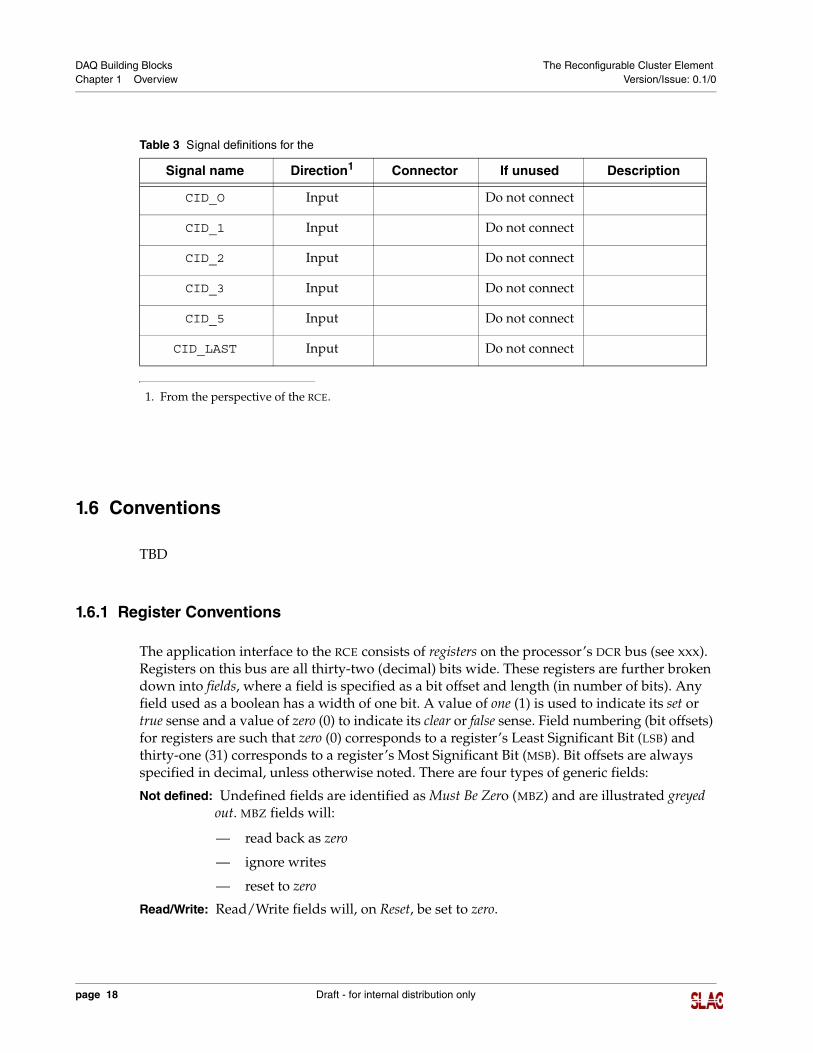
Table 3 p. 18 Signal definitions for the
Table 4 p. 22 Signal definitions for the JTAG Interface
Table 5 p. 23 Signal definitions for the PRGM Interface
Table 6 p. 23 Signal definitions for the BSI Interface
Table 7 p. 24 Signal definitions for the ETC Interface
Table 8 p. 25 Signal definitions for the BSI Interface
Table 9 p. 25 Signal definitions for the NRDY Interface
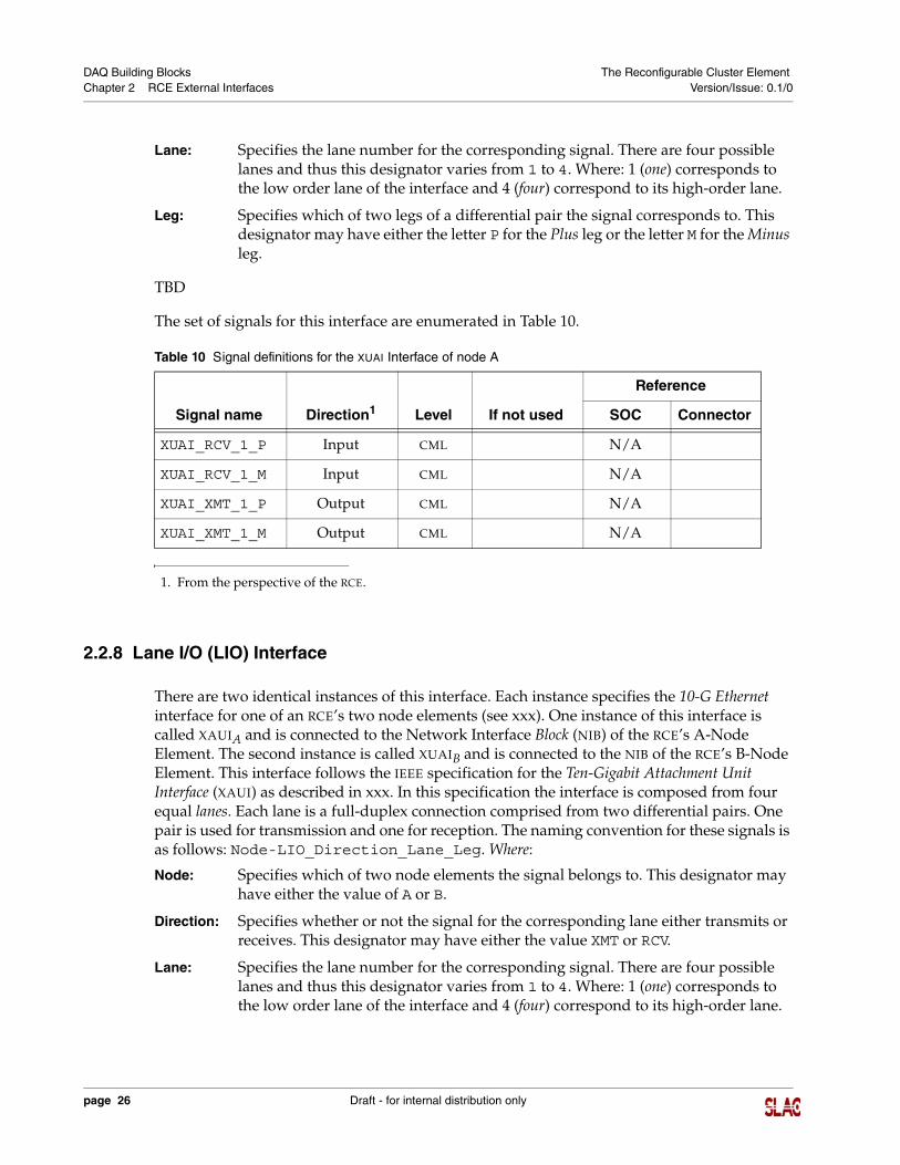
Table 10 p. 26 Signal definitions for the XUAI Interface of node A
Table 11 p. 27 Signal definitions for the base LIO Interface
Table 12 p. 27 Signal definitions for the base GPIO Interface
Table 13 p. 28 Signal definitions for the BSI Interface
Table 14 p. 29 Signal definitions for the XUAI Interface of node A
Table 15 p. 30 Signal definitions for the base LIO Interface
Table 16 p. 30 Signal definitions for the dual-Element GPIO Interface
Table 17 p. 31 Reserved signal definitions
Table 18 p. 31 Signal definitions for the base GPIO Interface
Table 19 p. 32 Reserved signal definitions
Table A.1 p. 43 Bill of Materials for Dual-Element mezzanine board
Table A.2 p. 47 Pin-outs for row one of the A-receive connector
Table A.3 p. 48 Pin-outs for row two of the A-receive connector
Table A.4 p. 49 Pin-outs for row one of the A-transmit connector
Draft - for internal distribution only page 13
DAQ Building Blocks The Reconfigurable Cluster Element List of Tables Version/Issue: 0.1/0
Table A.5 p. 50 Pin-outs for row two of the A-transmit connector
Table A.6 p. 52 Pin-outs for the Dual-element’s row one B-receive connector
Table A.7 p. 53 Pin-outs for the Dual-element’s row two B-receive connector
Table A.8 p. 54 Pin-outs for the Dual-element’s row one B-transmit connector
Table A.9 p. 55 Pin-outs for the Dual-element’s row one B-transmit connector
Table A.10 p. 58 Pin-outs for the Single-Element’s row one B-receive connector
Table A.11 p. 59 Pin-outs for the Single-Element’s row two B-receive connector
Table A.12 p. 60 Pin-outs for the Single-Element’s row one B-transmit connector
Table A.13 p. 61 Pin-outs for the Single-Element’s row two B-transmit connector
page 14 Draft - for internal distribution only
DAQ Building Blocks The Reconfigurable Cluster Element Chapter 1 Overview Version/Issue: 0.1/0
Chapter 1 Overview
1.1 Introduction
TBD
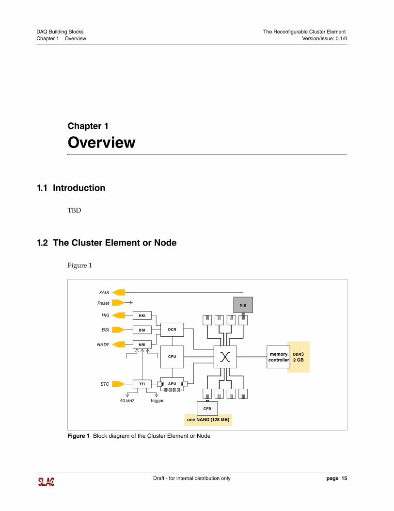
1.2 The Cluster Element or Node
Figure 1 Block diagram of the Cluster Element or Node
one NAND (128 MB)
DCR
controllerCPU
memory
NRI
TTI APU
40 MHZ
BSI
HKI
CFB
NIB
trigger
XAUI
HKI
BSI
NRDY
ETC
DDR32 GB
Reset
Figure 1
Draft - for internal distribution only page 15
DAQ Building Blocks The Reconfigurable Cluster Element Chapter 1 Overview Version/Issue: 0.1/0
TBD
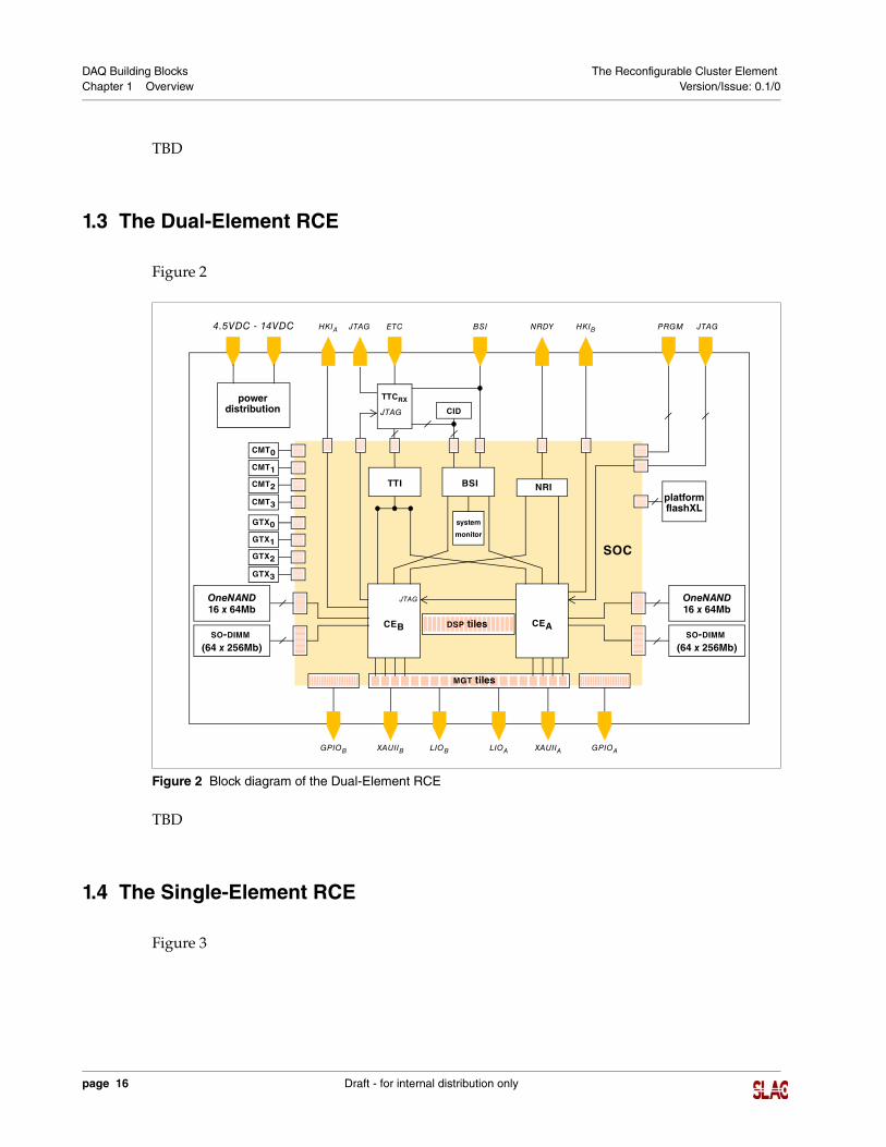
1.3 The Dual-Element RCE
Figure 2 Block diagram of the Dual-Element RCE
OneNAND16 x 64Mb
SO-DIMM
platform
XAUIIB
ETC HKIB
(64 x 256Mb)
system
monitor
OneNAND16 x 64Mb
SO-DIMM (64 x 256Mb)
DSP tiles
flashXL
PRGMHKIA JTAGNRDYBSI
CEA
MGT tiles
XAUIIAGPIOB LIOB LIOA GPIOA
BSI TTI
SOC
CEB
NRI
CID
GTX0
GTX1
GTX2
GTX3
CMT0
CMT1
CMT2
CMT3
JTAG
JTAG
TTCRX
JTAG
powerdistribution
4.5VDC - 14VDC
Figure 2
TBD
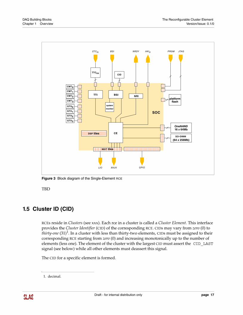
1.4 The Single-Element RCE
Figure 3
page 16 Draft - for internal distribution only
DAQ Building Blocks The Reconfigurable Cluster Element Chapter 1 Overview Version/Issue: 0.1/0
Figure 3 Block diagram of the Single-Element RCE
XAUIILIO
platform
TTCRX
ETCin HKIB
GTX0system
monitor
OneNAND16 x 64Mb
SO-DIMM (64 x 256Mb)
GTX1
GTX2
GTX3
DSP tiles
flash
PRGM JTAGNRDYBSI
CE
MGT tiles
GPIO
BSI TTI
SOC
NRI
CID
CMT0
CMT1
CMT2
CMT3
TBD
1.5 Cluster ID (CID)
RCEs reside in Clusters (see xxx). Each rce in a cluster is called a Cluster Element. This interface provides the Cluster Identifier (CID) of the corresponding RCE. CIDs may vary from zero (0) to thirty-one (31)1. In a cluster with less than thirty-two elements, CIDs must be assigned to their corresponding RCE starting from zero (0) and increasing monotonically up to the number of elements (less one). The element of the cluster with the largest CID must assert the CID_LAST signal (see below) while all other elements must deassert this signal.
The CID for a specific element is formed.
1. decimal.
Draft - for internal distribution only page 17
DAQ Building Blocks The Reconfigurable Cluster Element Chapter 1 Overview Version/Issue: 0.1/0
Table 3 Signal definitions for the
Signal name Direction1
1. From the perspective of the RCE.
CID_O Input Do not connect
CID_1 Input Do not connect
CID_2 Input Do not connect
CID_3 Input Do not connect
CID_5 Input Do not connect
CID_LAST Input Do not connect
1.6 Conventions
TBD
1.6.1 Register Conventions
The application interface to the RCE consists of registers on the processor’s DCR bus (see xxx). Registers on this bus are all thirty-two (decimal) bits wide. These registers are further broken down into fields, where a field is specified as a bit offset and length (in number of bits). Any field used as a boolean has a width of one bit. A value of one (1) is used to indicate its set or true sense and a value of zero (0) to indicate its clear or false sense. Field numbering (bit offsets) for registers are such that zero (0) corresponds to a register’s Least Significant Bit (LSB) and thirty-one (31) corresponds to a register’s Most Significant Bit (MSB). Bit offsets are always specified in decimal, unless otherwise noted. There are four types of generic fields:
Not defined: Undefined fields are identified as Must Be Zero (MBZ) and are illustrated greyed out. MBZ fields will:
— read back as zero
— ignore writes
— reset to zero
Read/Write: Read/Write fields will, on Reset, be set to zero.
Connector If unused Description
page 18 Draft - for internal distribution only
DAQ Building Blocks The Reconfigurable Cluster Element Chapter 1 Overview Version/Issue: 0.1/0
Selective Set and Clear (SSC): SSC fields are used where it is necessary to change one or more fields of a register and leave the remaining fields unchanged1. These fields will have a complementing Enable field. This field will have the same width as its corresponding SSC field. The Enable field for any arbitrary SSC field is found by shifting that field’s bit offset by 16 (decimal). Enable fields are illustrated lightly greyed-out. These fields satisfy the following conventions:
— may only be set, clearing the field is ignored
— read back as zero
SSC fields will:
— ignore writes, unless their corresponding field enables are also asserted
— reset to zero, unless otherwise documented
Read-Only: Read-only fields are illustrated lightly greyed-out with their value. Read-Only fields will:
— ignore writes
— reset to zero, unless otherwise documented
Registers on the DCR bus are read using the mfdcr instruction and written using the mtdcr instruction. The literal offset of these instructions corresponds to the register’s bus address.
1. Sometimes referred to as indivisible read/modify/write.
Draft - for internal distribution only page 19
DAQ Building Blocks The Reconfigurable Cluster Element Chapter 1 Overview Version/Issue: 0.1/0
page 20 Draft - for internal distribution only
DAQ Building Blocks The Reconfigurable Cluster Element Chapter 2 RCE External Interfaces Version/Issue: 0.1/0
Chapter 2 RCE External Interfaces
2.1 Introduction
TBD.
2.2 Base Interface
TBD.
2.2.1 JTAG Interface
This interface constitutes the head of a JTAG chain composed of the JTAG devices internal to the RCE: These include:
— The SOC.
— The TTCRX.
— The configuration flash.
— The processor debug interface (see xxx) for each element.
The set of signals for this interface are enumerated in Table 4. Following that table are a detailed description of each signal.
Draft - for internal distribution only page 21
DAQ Building Blocks The Reconfigurable Cluster Element Chapter 2 RCE External Interfaces Version/Issue: 0.1/0
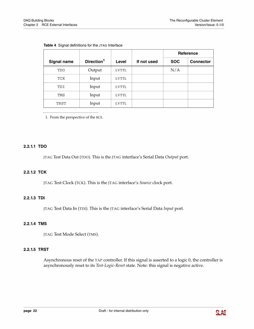
Table 4 Signal definitions for the JTAG Interface
Signal name Direction1
1. From the perspective of the RCE.
TDO Output LVTTL N/A
TCK Input LVTTL
TDI Input LVTTL
TMS Input LVTTL
TRST Input LVTTL
2.2.1.1 TDO
JTAG Test Data Out (TDO). This is the JTAG interface’s Serial Data Output port.
2.2.1.2 TCK
JTAG Test Clock (TCK). This is the JTAG interface’s Source clock port.
2.2.1.3 TDI
JTAG Test Data In (TDI). This is the JTAG interface’s Serial Data Input port.
2.2.1.4 TMS
JTAG Test Mode Select (TMS).
2.2.1.5 TRST
Asynchronous reset of the TAP controller. If this signal is asserted to a logic 0, the controller is asynchronously reset to its Test-Logic-Reset state. Note: this signal is negative active.
Level If not used
Reference
SOC Connector
page 22 Draft - for internal distribution only
DAQ Building Blocks The Reconfigurable Cluster Element Chapter 2 RCE External Interfaces Version/Issue: 0.1/0
2.2.2 Program Interface (PRGM)
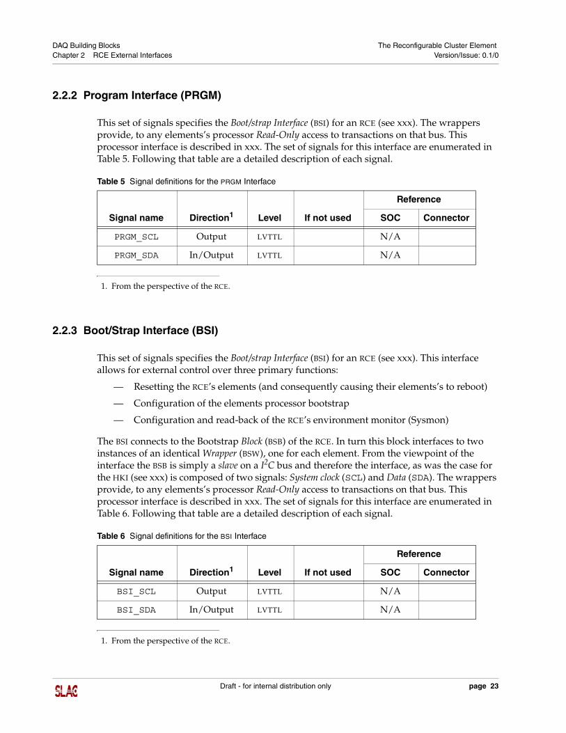
Table 5 Signal definitions for the PRGM Interface
Signal name Direction1
1. From the perspective of the RCE.
PRGM_SCL Output LVTTL N/A
PRGM_SDA In/Output LVTTL N/A
This set of signals specifies the Boot/strap Interface (BSI) for an RCE (see xxx). The wrappers provide, to any elements’s processor Read-Only access to transactions on that bus. This processor interface is described in xxx. The set of signals for this interface are enumerated in Table 5. Following that table are a detailed description of each signal.
2.2.3 Boot/Strap Interface (BSI)
This set of signals specifies the Boot/strap Interface (BSI) for an RCE (see xxx). This interface allows for external control over three primary functions:
— Resetting the RCE’s elements (and consequently causing their elements’s to reboot)
— Configuration of the elements processor bootstrap
— Configuration and read-back of the RCE’s environment monitor (Sysmon)
Table 6 Signal definitions for the BSI Interface
Signal name Direction1
1. From the perspective of the RCE.
BSI_SCL Output LVTTL N/A
BSI_SDA In/Output LVTTL N/A
The BSI connects to the Bootstrap Block (BSB) of the RCE. In turn this block interfaces to two instances of an identical Wrapper (BSW), one for each element. From the viewpoint of the interface the BSB is simply a slave on a I2C bus and therefore the interface, as was the case for the HKI (see xxx) is composed of two signals: System clock (SCL) and Data (SDA). The wrappers provide, to any elements’s processor Read-Only access to transactions on that bus. This processor interface is described in xxx. The set of signals for this interface are enumerated in Table 6. Following that table are a detailed description of each signal.
Level If not used
Reference
SOC Connector
Level If not used
Reference
SOC Connector
Draft - for internal distribution only page 23
DAQ Building Blocks The Reconfigurable Cluster Element Chapter 2 RCE External Interfaces Version/Issue: 0.1/0
2.2.4 Encoded Timing Channel (ETC) Interface
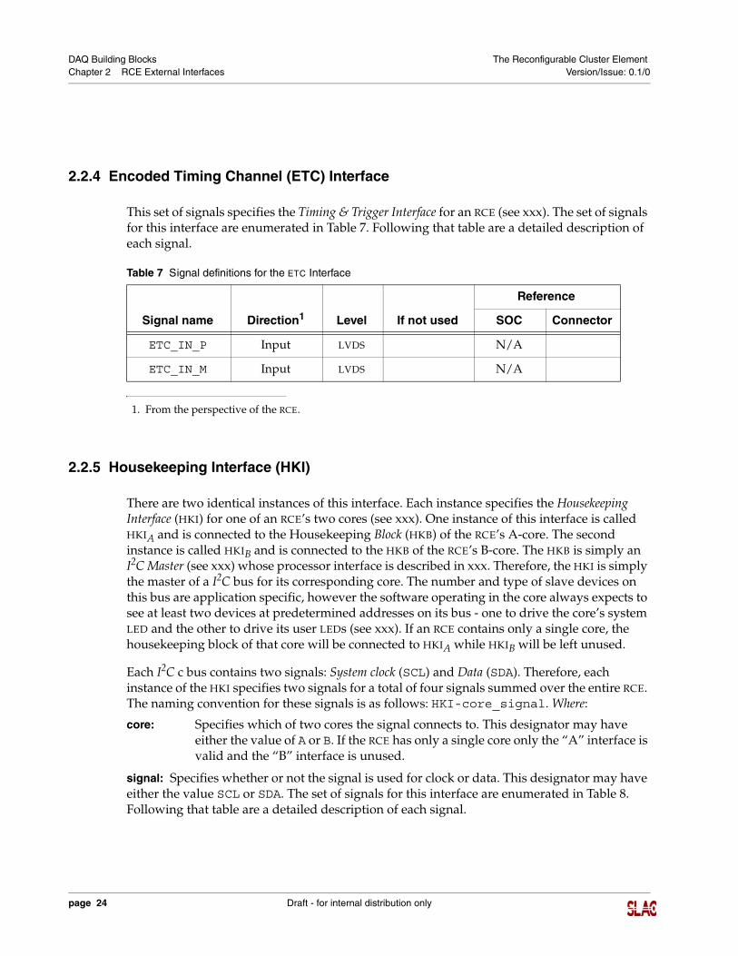
Table 7 Signal definitions for the ETC Interface
Signal name Direction1
1. From the perspective of the RCE.
ETC_IN_P Input LVDS N/A
ETC_IN_M Input LVDS N/A
This set of signals specifies the Timing & Trigger Interface for an RCE (see xxx). The set of signals for this interface are enumerated in Table 7. Following that table are a detailed description of each signal.
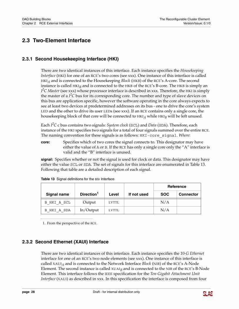
2.2.5 Housekeeping Interface (HKI)
There are two identical instances of this interface. Each instance specifies the Housekeeping Interface (HKI) for one of an RCE’s two cores (see xxx). One instance of this interface is called HKIA and is connected to the Housekeeping Block (HKB) of the RCE’s A-core. The second instance is called HKIB and is connected to the HKB of the RCE’s B-core. The HKB is simply an I2C Master (see xxx) whose processor interface is described in xxx. Therefore, the HKI is simply the master of a I2C bus for its corresponding core. The number and type of slave devices on this bus are application specific, however the software operating in the core always expects to see at least two devices at predetermined addresses on its bus - one to drive the core’s system LED and the other to drive its user LEDs (see xxx). If an RCE contains only a single core, the housekeeping block of that core will be connected to HKIA while HKIB will be left unused.
Each I2C c bus contains two signals: System clock (SCL) and Data (SDA). Therefore, each instance of the HKI specifies two signals for a total of four signals summed over the entire RCE. The naming convention for these signals is as follows: HKI-core_signal. Where:
core: Specifies which of two cores the signal connects to. This designator may have either the value of A or B. If the RCE has only a single core only the “A” interface is valid and the “B” interface is unused.
signal: Specifies whether or not the signal is used for clock or data. This designator may have either the value SCL or SDA. The set of signals for this interface are enumerated in Table 8. Following that table are a detailed description of each signal.
Level If not used
Reference
SOC Connector
page 24 Draft - for internal distribution only
DAQ Building Blocks The Reconfigurable Cluster Element Chapter 2 RCE External Interfaces Version/Issue: 0.1/0
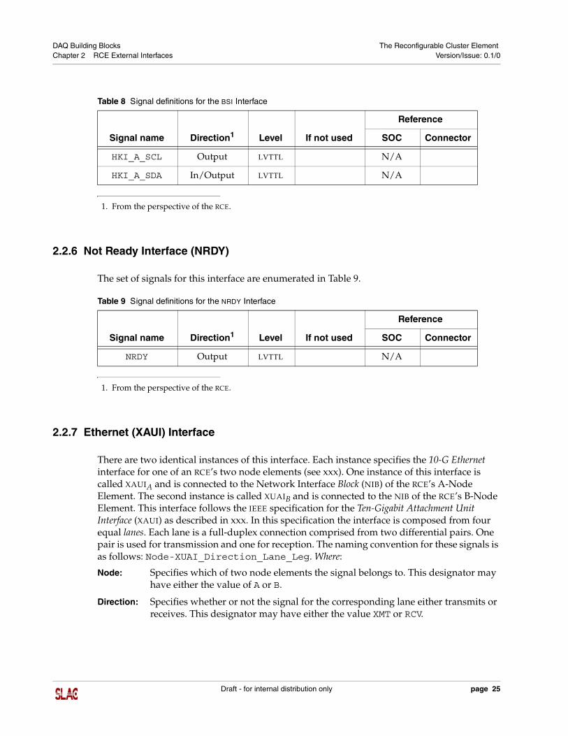
Table 8 Signal definitions for the BSI Interface
Signal name Direction1
1. From the perspective of the RCE.
HKI_A_SCL Output LVTTL N/A
HKI_A_SDA In/Output LVTTL N/A
2.2.6 Not Ready Interface (NRDY)
Table 9 Signal definitions for the NRDY Interface
Signal name Direction1
1. From the perspective of the RCE.
NRDY Output LVTTL N/A
The set of signals for this interface are enumerated in Table 9.
2.2.7 Ethernet (XAUI) Interface
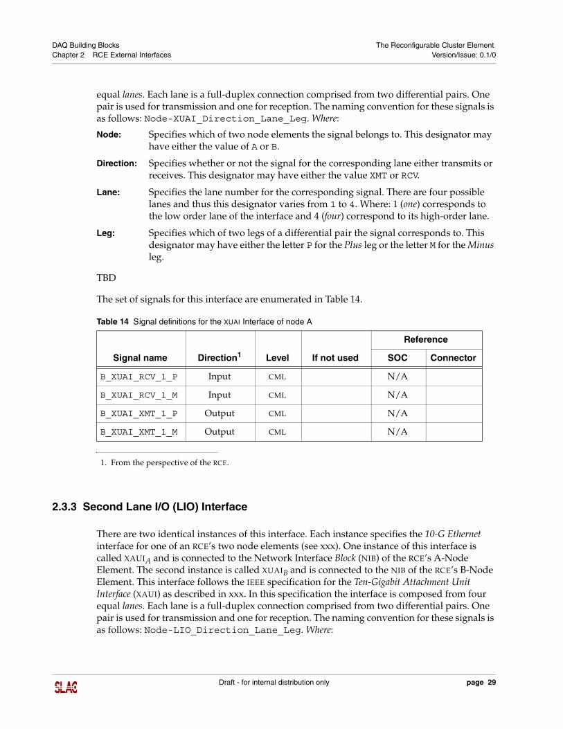
There are two identical instances of this interface. Each instance specifies the 10-G Ethernet interface for one of an RCE’s two node elements (see xxx). One instance of this interface is called XAUIA and is connected to the Network Interface Block (NIB) of the RCE’s A-Node Element. The second instance is called XUAIB and is connected to the NIB of the RCE’s B-Node Element. This interface follows the IEEE specification for the Ten-Gigabit Attachment Unit Interface (XAUI) as described in xxx. In this specification the interface is composed from four equal lanes. Each lane is a full-duplex connection comprised from two differential pairs. One pair is used for transmission and one for reception. The naming convention for these signals is as follows: Node-XUAI_Direction_Lane_Leg. Where:
Node: Specifies which of two node elements the signal belongs to. This designator may have either the value of A or B.
Direction: Specifies whether or not the signal for the corresponding lane either transmits or receives. This designator may have either the value XMT or RCV.
Level If not used
Reference
SOC Connector
Level If not used
Reference
SOC Connector
Draft - for internal distribution only page 25
DAQ Building Blocks The Reconfigurable Cluster Element Chapter 2 RCE External Interfaces Version/Issue: 0.1/0
Lane: Specifies the lane number for the corresponding signal. There are four possible lanes and thus this designator varies from 1 to 4. Where: 1 (one) corresponds to the low order lane of the interface and 4 (four) correspond to its high-order lane.
Leg: Specifies which of two legs of a differential pair the signal corresponds to. This designator may have either the letter P for the Plus leg or the letter M for the Minus leg.
Table 10 Signal definitions for the XUAI Interface of node A
Signal name Direction1
1. From the perspective of the RCE.
XUAI_RCV_1_P Input CML N/A
XUAI_RCV_1_M Input CML N/A
XUAI_XMT_1_P Output CML N/A
XUAI_XMT_1_M Output CML N/A
TBD
The set of signals for this interface are enumerated in Table 10.
2.2.8 Lane I/O (LIO) Interface
There are two identical instances of this interface. Each instance specifies the 10-G Ethernet interface for one of an RCE’s two node elements (see xxx). One instance of this interface is called XAUIA and is connected to the Network Interface Block (NIB) of the RCE’s A-Node Element. The second instance is called XUAIB and is connected to the NIB of the RCE’s B-Node Element. This interface follows the IEEE specification for the Ten-Gigabit Attachment Unit Interface (XAUI) as described in xxx. In this specification the interface is composed from four equal lanes. Each lane is a full-duplex connection comprised from two differential pairs. One pair is used for transmission and one for reception. The naming convention for these signals is as follows: Node-LIO_Direction_Lane_Leg. Where:
Node: Specifies which of two node elements the signal belongs to. This designator may have either the value of A or B.
Direction: Specifies whether or not the signal for the corresponding lane either transmits or receives. This designator may have either the value XMT or RCV.
Lane: Specifies the lane number for the corresponding signal. There are four possible lanes and thus this designator varies from 1 to 4. Where: 1 (one) corresponds to the low order lane of the interface and 4 (four) correspond to its high-order lane.
Level If not used
Reference
SOC Connector
page 26 Draft - for internal distribution only
DAQ Building Blocks The Reconfigurable Cluster Element Chapter 2 RCE External Interfaces Version/Issue: 0.1/0
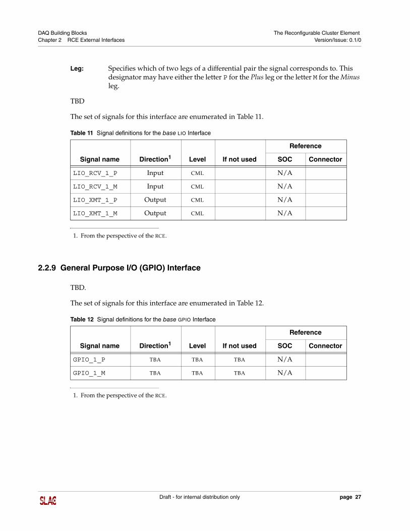
Leg: Specifies which of two legs of a differential pair the signal corresponds to. This designator may have either the letter P for the Plus leg or the letter M for the Minus leg.
Table 11 Signal definitions for the base LIO Interface
Signal name Direction1
1. From the perspective of the RCE.
LIO_RCV_1_P Input CML N/A
LIO_RCV_1_M Input CML N/A
LIO_XMT_1_P Output CML N/A
LIO_XMT_1_M Output CML N/A
TBD
The set of signals for this interface are enumerated in Table 11.
2.2.9 General Purpose I/O (GPIO) Interface
Table 12 Signal definitions for the base GPIO Interface
Signal name Direction1
1. From the perspective of the RCE.
GPIO_1_P TBA TBA TBA N/A
GPIO_1_M TBA TBA TBA N/A
TBD.
The set of signals for this interface are enumerated in Table 12.
Level If not used
Reference
SOC Connector
Level If not used
Reference
SOC Connector
Draft - for internal distribution only page 27
DAQ Building Blocks The Reconfigurable Cluster Element Chapter 2 RCE External Interfaces Version/Issue: 0.1/0
2.3 Two-Element Interface
2.3.1 Second Housekeeping Interface (HKI)
There are two identical instances of this interface. Each instance specifies the Housekeeping Interface (HKI) for one of an RCE’s two cores (see xxx). One instance of this interface is called HKIA and is connected to the Housekeeping Block (HKB) of the RCE’s A-core. The second instance is called HKIB and is connected to the HKB of the RCE’s B-core. The HKB is simply an I2C Master (see xxx) whose processor interface is described in xxx. Therefore, the HKI is simply the master of a I2C bus for its corresponding core. The number and type of slave devices on this bus are application specific, however the software operating in the core always expects to see at least two devices at predetermined addresses on its bus - one to drive the core’s system LED and the other to drive its user LEDs (see xxx). If an RCE contains only a single core, the housekeeping block of that core will be connected to HKIA while HKIB will be left unused.
Each I2C c bus contains two signals: System clock (SCL) and Data (SDA). Therefore, each instance of the HKI specifies two signals for a total of four signals summed over the entire RCE. The naming convention for these signals is as follows: HKI-core_signal. Where:
core: Specifies which of two cores the signal connects to. This designator may have either the value of A or B. If the RCE has only a single core only the “A” interface is valid and the “B” interface is unused.
signal:
Table 13 Signal definitions for the BSI Interface
Signal name Direction1
1. From the perspective of the RCE.
B_HKI_A_SCL Output LVTTL N/A
B_HKI_A_SDA In/Output LVTTL N/A
Specifies whether or not the signal is used for clock or data. This designator may have either the value SCL or SDA. The set of signals for this interface are enumerated in Table 13. Following that table are a detailed description of each signal.
2.3.2 Second Ethernet (XAUI) Interface
There are two identical instances of this interface. Each instance specifies the 10-G Ethernet interface for one of an RCE’s two node elements (see xxx). One instance of this interface is called XAUIA and is connected to the Network Interface Block (NIB) of the RCE’s A-Node Element. The second instance is called XUAIB and is connected to the NIB of the RCE’s B-Node Element. This interface follows the IEEE specification for the Ten-Gigabit Attachment Unit Interface (XAUI) as described in xxx. In this specification the interface is composed from four
Level If not used
Reference
SOC Connector
page 28 Draft - for internal distribution only
DAQ Building Blocks The Reconfigurable Cluster Element Chapter 2 RCE External Interfaces Version/Issue: 0.1/0
equal lanes. Each lane is a full-duplex connection comprised from two differential pairs. One pair is used for transmission and one for reception. The naming convention for these signals is as follows: Node-XUAI_Direction_Lane_Leg. Where:
Node: Specifies which of two node elements the signal belongs to. This designator may have either the value of A or B.
Direction: Specifies whether or not the signal for the corresponding lane either transmits or receives. This designator may have either the value XMT or RCV.
Lane: Specifies the lane number for the corresponding signal. There are four possible lanes and thus this designator varies from 1 to 4. Where: 1 (one) corresponds to the low order lane of the interface and 4 (four) correspond to its high-order lane.
Leg: Specifies which of two legs of a differential pair the signal corresponds to. This designator may have either the letter P for the Plus leg or the letter M for the Minus leg.
Table 14 Signal definitions for the XUAI Interface of node A
Signal name Direction1
1. From the perspective of the RCE.
B_XUAI_RCV_1_P Input CML N/A
B_XUAI_RCV_1_M Input CML N/A
B_XUAI_XMT_1_P Output CML N/A
B_XUAI_XMT_1_M Output CML N/A
TBD
The set of signals for this interface are enumerated in Table 14.
2.3.3 Second Lane I/O (LIO) Interface
There are two identical instances of this interface. Each instance specifies the 10-G Ethernet interface for one of an RCE’s two node elements (see xxx). One instance of this interface is called XAUIA and is connected to the Network Interface Block (NIB) of the RCE’s A-Node Element. The second instance is called XUAIB and is connected to the NIB of the RCE’s B-Node Element. This interface follows the IEEE specification for the Ten-Gigabit Attachment Unit Interface (XAUI) as described in xxx. In this specification the interface is composed from four equal lanes. Each lane is a full-duplex connection comprised from two differential pairs. One pair is used for transmission and one for reception. The naming convention for these signals is as follows: Node-LIO_Direction_Lane_Leg. Where:
Level If not used
Reference
SOC Connector
Draft - for internal distribution only page 29
DAQ Building Blocks The Reconfigurable Cluster Element Chapter 2 RCE External Interfaces Version/Issue: 0.1/0
Node: Specifies which of two node elements the signal belongs to. This designator may have either the value of A or B.
Direction: Specifies whether or not the signal for the corresponding lane either transmits or receives. This designator may have either the value XMT or RCV.
Lane: Specifies the lane number for the corresponding signal. There are four possible lanes and thus this designator varies from 1 to 4. Where: 1 (one) corresponds to the low order lane of the interface and 4 (four) correspond to its high-order lane.
Leg: Specifies which of two legs of a differential pair the signal corresponds to. This designator may have either the letter P for the Plus leg or the letter M for the Minus leg.
Table 15 Signal definitions for the base LIO Interface
Signal name Direction1
1. From the perspective of the RCE.
B_LIO_RCV_1_P Input CML N/A
B_LIO_RCV_1_M Input CML N/A
B_LIO_XMT_1_P Output CML N/A
B_LIO_XMT_1_M Output CML N/A
TBD
The set of signals for this interface are enumerated in Table 15.
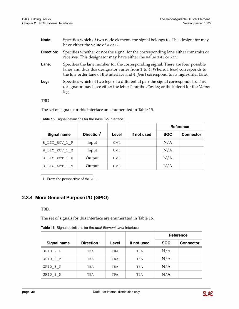
2.3.4 More General Purpose I/O (GPIO)
Table 16 Signal definitions for the dual-Element GPIO Interface
Signal name Direction1 Level If not used
Reference
SOC Connector
GPIO_2_P TBA TBA TBA N/A
GPIO_2_M TBA TBA TBA N/A
GPIO_3_P TBA TBA TBA N/A
GPIO_3_M TBA TBA TBA N/A
TBD.
The set of signals for this interface are enumerated in Table 16.
Level If not used
Reference
SOC Connector
page 30 Draft - for internal distribution only
DAQ Building Blocks The Reconfigurable Cluster Element Chapter 2 RCE External Interfaces Version/Issue: 0.1/0
2.3.5 Reserved Signals (RSVD)
Table 17 Reserved signal definitions
Signal name Direction1
1. From the perspective of the RCE.
RSVD_1 N/A TBA N/A
There are two identical instances of this interface. The set of signals for this interface are enumerated in Table 17.
2.4 Single-Element Interface
2.4.1 More General Purpose I/O (GPIO)
Table 18 Signal definitions for the base GPIO Interface
Signal name Direction1
1. From the perspective of the RCE.
GPIO_2_P TBA TBA TBA N/A
GPIO_2_M TBA TBA TBA N/A
GPIO_3_P TBA TBA TBA N/A
GPIO_3_M TBA TBA TBA N/A
TBD.
The set of signals for this interface are enumerated in Table 18.
1. From the perspective of the RCE.
Level If not used
Reference
SOC Connector
Level If not used
Reference
SOC Connector
Draft - for internal distribution only page 31
DAQ Building Blocks The Reconfigurable Cluster Element Chapter 2 RCE External Interfaces Version/Issue: 0.1/0
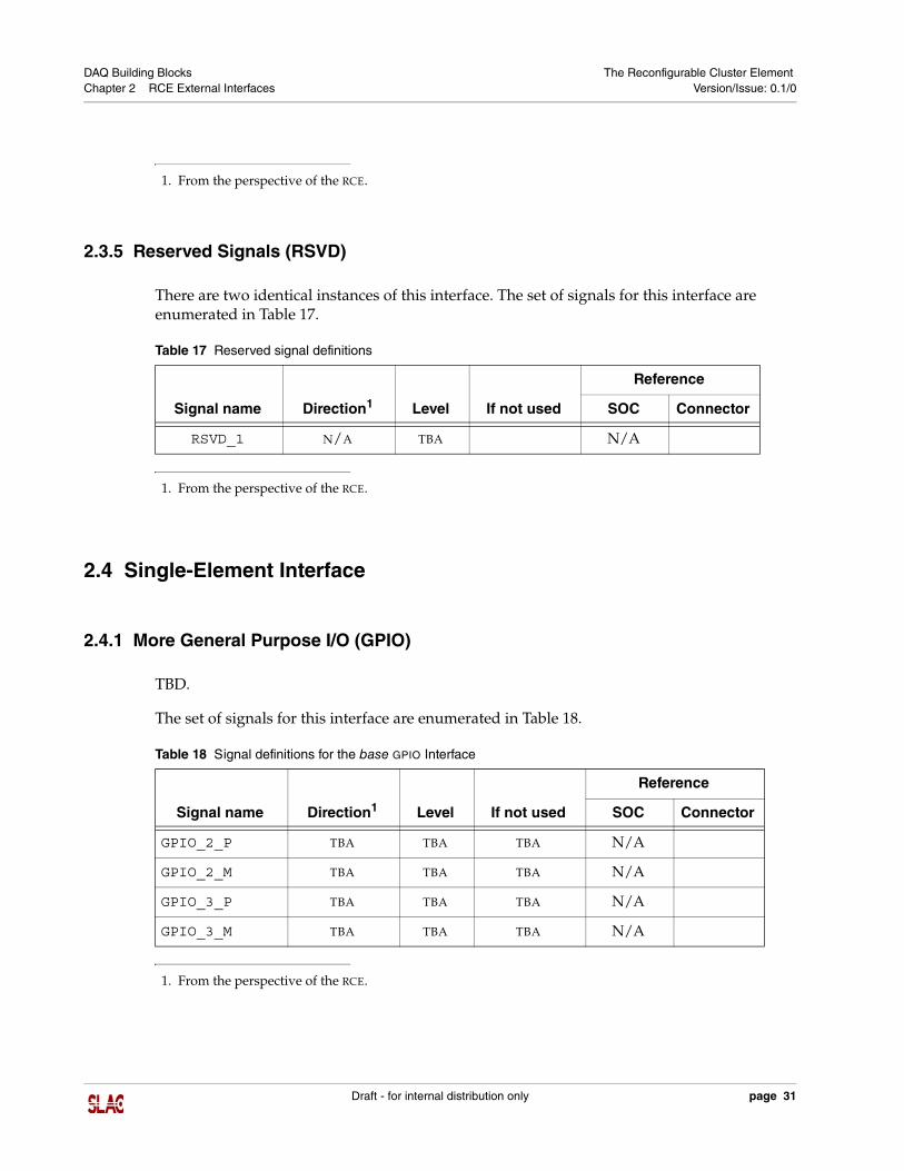
2.4.2 Reserved Signals (RSVD)
Table 19 Reserved signal definitions
Signal name Direction1
1. From the perspective of the RCE.
RSVD_1 N/A TBA N/A
There are two identical instances of this interface. The set of signals for this interface are enumerated in Table 19.
Level If not used
Reference
SOC Connector
page 32 Draft - for internal distribution only
DAQ Building Blocks The Reconfigurable Cluster Element Chapter 3 Bootstrap Interface (BSI) Version/Issue: 0.1/0
Chapter 3 Bootstrap Interface (BSI)
3.1 Introduction
TBD.
Draft - for internal distribution only page 33
DAQ Building Blocks The Reconfigurable Cluster Element Chapter 3 Bootstrap Interface (BSI) Version/Issue: 0.1/0
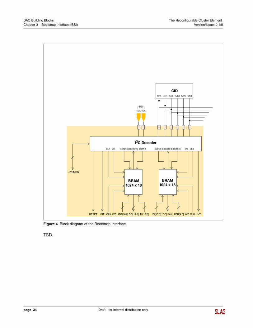
Figure 4 Block diagram of the Bootstrap Interface
DO[15:0]
ID[0] ID[1] ID[2] ID[3] ID[4] ID[5]
SDA SCL
BSI
CID
I2C Decoder
DI[15:0]WECLK ADR[9:0] DO[15:0]DI[15:0] WE CLKADR[9:0]INTRESET
WECLK WE CLKDI[17:0]DO[17:0]ADR[9:0] DI[17:0]DO[17:0]ADR[9:0]
BRAM1024 x 18
BRAM1024 x 18
INT
SYSMON
TBD.
page 34 Draft - for internal distribution only
DAQ Building Blocks The Reconfigurable Cluster Element Chapter 4 Timing & Trigger Interface (TTI) Version/Issue: 0.1/0
Chapter 4 Timing & Trigger Interface (TTI)
4.1 Introduction
TBD.
Draft - for internal distribution only page 35
DAQ Building Blocks The Reconfigurable Cluster Element Chapter 4 Timing & Trigger Interface (TTI) Version/Issue: 0.1/0
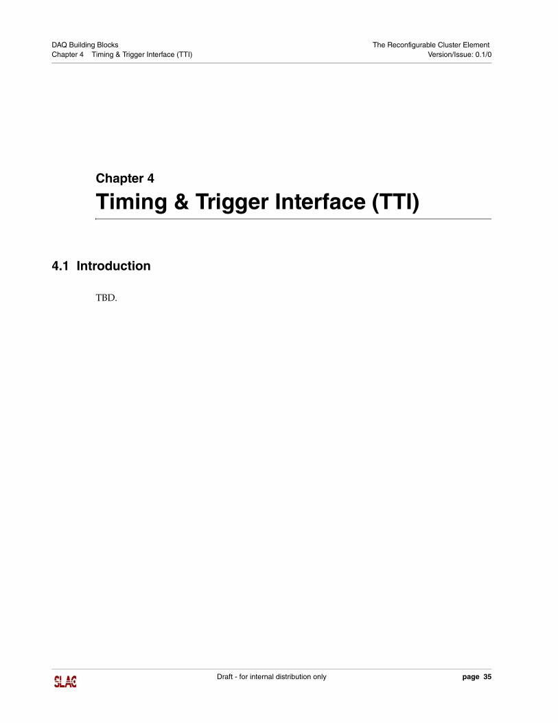
Figure 5 Timing & Trigger Interface
ETM_S
SubAddr<7:0>
ETM<35:0> TRG RST_EC RST_BCCLK
ID[:0] ID[:1] ID[:2] ID[:0] ID[:0] ID[:0]
Dout<0>
Dout<1>
Dout<2>
Dout<3>
Dout<4>
Dout<5>
Dout<6:7>
JTAGTDI
JTAGRST
SDA SCL
SDA
SCL
JTAGTMS
JTAGTCK
JTAGTDO
TDO
ETC
In & In_b
Reset_b
SYS[3:0] SYS_S
BrcstStr2Brcst<7:6>Clock40Des2
USR_S USR<1:0>CLK
TTCready
RDYRESET
EvCntLstr L1Accept BCntResBCntStrBCnt<11:0> EvCntHstrClock40Des1 ECntRes Brcst<5:2> BrcstStr1
TDOTCKTMSRST
BSIJTAG
CID
TTCRX
TTITTITTITTI
TBD.
page 36 Draft - for internal distribution only
DAQ Building Blocks The Reconfigurable Cluster Element Chapter 5 Power Distribution Version/Issue: 0.1/0
Chapter 5 Power Distribution
5.1 Introduction
TBD.
Draft - for internal distribution only page 37
DAQ Building Blocks The Reconfigurable Cluster Element Chapter 5 Power Distribution Version/Issue: 0.1/0
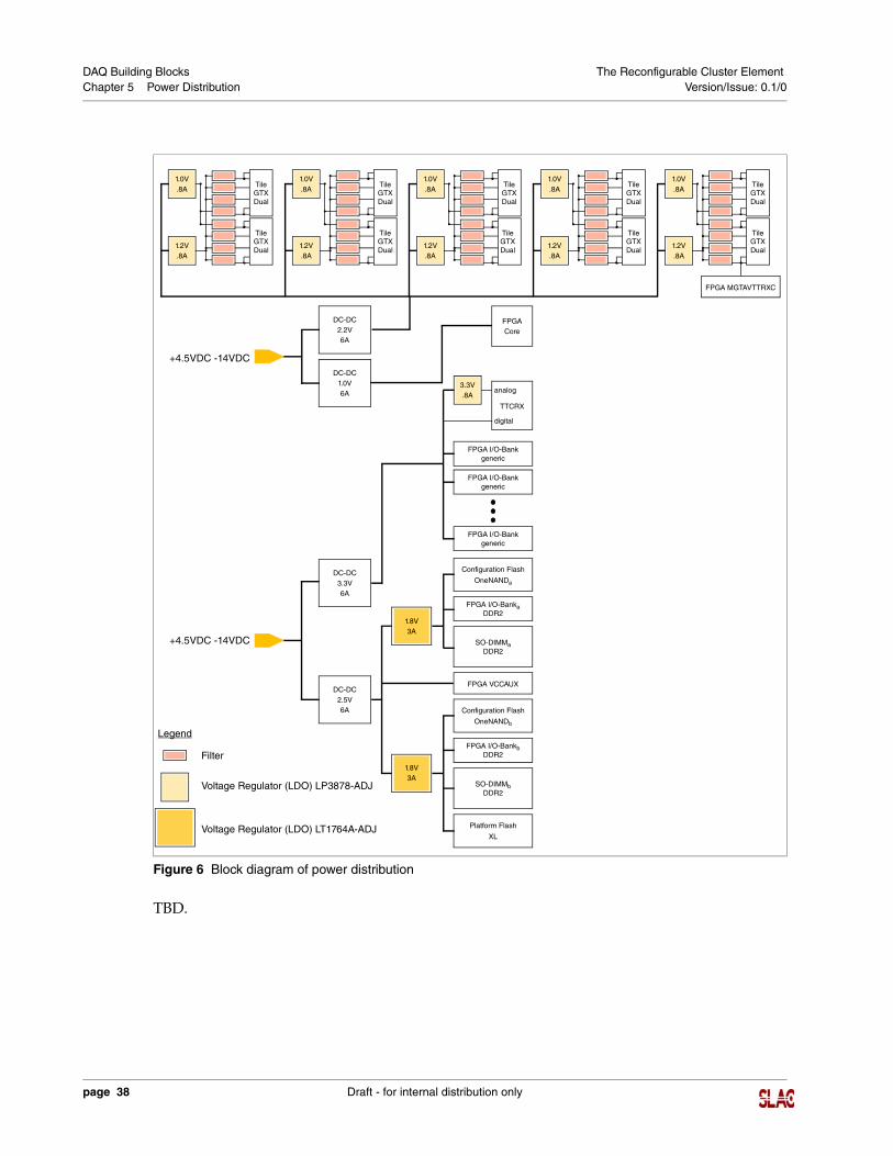
Figure 6 Block diagram of power distribution
OneNANDa
SO-DIMMaDDR2
Dual
FPGA I/O-BankaDDR2
GTXTile
DualGTXTile
DualGTXTile
DualGTXTile
DualGTXTile
DualGTXTile
DualGTXTile
DualGTXTile
DualGTXTile
DualGTXTile
Configuration Flash
TTCRX
OneNANDb
SO-DIMMbDDR2
FPGA I/O-BankbDDR2
Configuration Flash
XL
Platform Flash
FPGA I/O-Bankgeneric
FPGA I/O-Bankgeneric
FPGA I/O-Bankgeneric
analog
digital
FPGACore
FPGA VCCAUX
DC-DC2.2V6A
DC-DC1.0V6A
DC-DC3.3V6A
DC-DC2.5V6A
1.8V3A
1.8V3A
3.3V.8A
1.0V.8A
1.2V.8A
1.0V.8A
1.2V.8A
1.0V.8A
1.2V.8A
1.0V.8A
1.2V.8A
1.0V.8A
1.2V.8A
+4.5VDC -14VDC
+4.5VDC -14VDC
FPGA MGTAVTTRXC
Legend
Filter
Voltage Regulator (LDO) LP3878-ADJ
Voltage Regulator (LDO) LT1764A-ADJ
TBD.
page 38 Draft - for internal distribution only

DAQ Building Blocks The Reconfigurable Cluster Element Chapter 6 Not Ready Interface (NRI) Version/Issue: 0.1/0
Chapter 6 Not Ready Interface (NRI)
6.1 Introduction
TBD.
Draft - for internal distribution only page 39
DAQ Building Blocks The Reconfigurable Cluster Element Chapter 6 Not Ready Interface (NRI) Version/Issue: 0.1/0
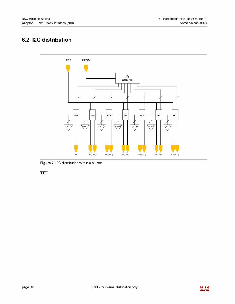
6.2 I2C distribution
Figure 7 I2C distribution within a cluster
CIM
I2C GPIO (16)
BSI
RCE RCE RCE RCE RCE RCE
CID 0
HKIA
CID 1 CID 6CID 5CID 2 CID 4CID 3
HKIBHKIA HKIB HKIA HKIB HKIA HKIB HKIA HKIBHKIA HKIBHKI
PRGM
TBD.
page 40 Draft - for internal distribution only
DAQ Building Blocks The Reconfigurable Cluster Element Appendix A RCE Mezzanine Boards Version/Issue: 0.1/0
Appendix A RCE Mezzanine Boards
A.1 Introduction
The RCE is realized on two different types of mezzanine boards corresponding to the two different types of RCEs, either Single or Dual-Element (see xxx). Each board consists of its appropriate components plus six connectors which export the physical interface described in Chapter 2. Although certainly appropriate for usage in isolation, these boards are optimized for their usage in a Cluster as described in xxx.
A.1.1 Connector numerology
Independent of type, each board shares identical connectors. Two of these connectors carry power and ground, while the other four carry the various interface signals. Two signal connectors are paired with one power connector to form one group. Thus a board has two groups. One group is called the A-Connectors and the second group the B-Connectors.
For power & ground boards employ the ERNI MicroSpeed Power Module connector (see xxx). This connector has five pins (exclusive of ground) arranged in a single row. It is designed to carry up to twelve amps of current with its form-factor designed to match the signal connectors described below. Its pin-outs are specified in Section A.2.
For interface signals boards employ connectors from the ERNI MicroSpeed 1.0 mm High Speed Mezzanine Connector family (see xxx). These connectors have fifty (50) pins arranged in two rows and are designed to operate at signalling speeds up to 10-Gb/sec. The A-Signal connectors, independent of board type always share identical pin-outs and carry the Base interface described in Chapter 2, Section 2.2. However, the pin-outs of the B-Signal connectors varies depending on whether used in a Single or Dual-Element board. Reflecting their principal function the two connectors of a group are labelled as either a receive or a transmit connector. The pin-out for A-Signal connectors are enumerated and described in Section A.2, while the B-Signal connectors for the Dual-Element board are specified in Section A.4 and the
Draft - for internal distribution only page 41
DAQ Building Blocks The Reconfigurable Cluster Element Appendix A RCE Mezzanine Boards Version/Issue: 0.1/0
Figure A.1 Mezzanine board connector naming conventions
Transmit Receive
A-Connectors
B-Connectors
Power
Transmit ReceivePower
Single-Element board in Section A.4.6. An idealized layout of either board’s six connectors showing their naming conventions is illustrated in Figure A.1:
TBD
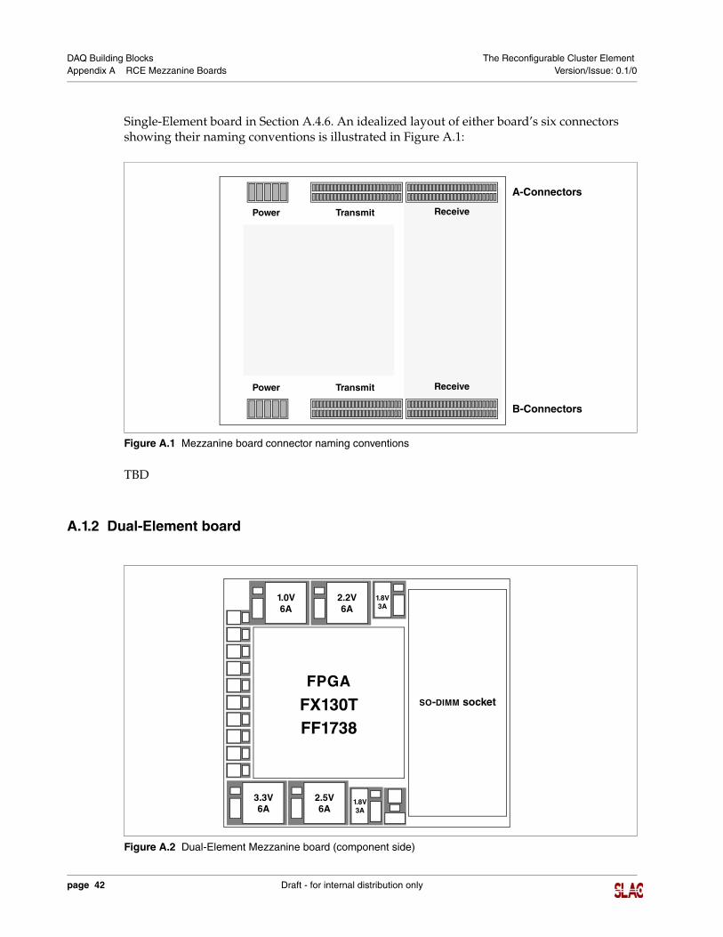
A.1.2 Dual-Element board
Figure A.2 Dual-Element Mezzanine board (component side)
SO-DIMM socket
FF1738
FPGA
FX130T
3.3V 2.5V
1.0V 2.2V
1.0V
1.2
1.2
1.2
1.2
1.0
1.0
1.0
1.0
1.8V3A
1.8V3A6A6A
6A 6A
page 42 Draft - for internal distribution only
DAQ Building Blocks The Reconfigurable Cluster Element Appendix A RCE Mezzanine Boards Version/Issue: 0.1/0
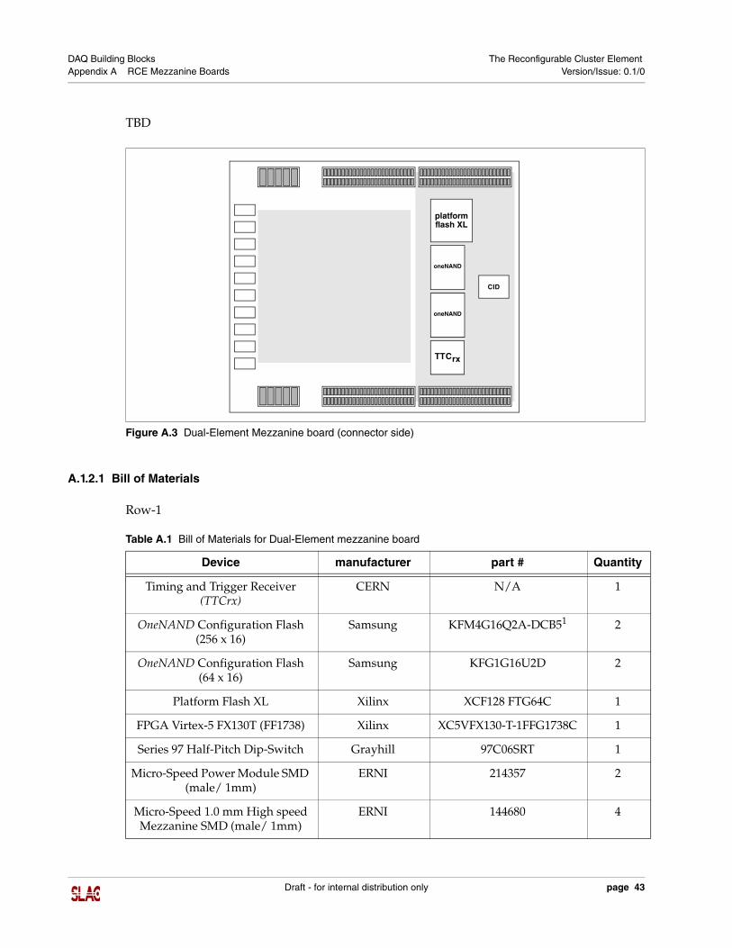
Figure A.3 Dual-Element Mezzanine board (connector side)
TTCrx
platformflash XL
oneNAND
oneNAND
CID
TBD
A.1.2.1 Bill of Materials
Row-1
Table A.1 Bill of Materials for Dual-Element mezzanine board
Device manufacturer part # Quantity
Timing and Trigger Receiver (TTCrx)
CERN N/A 1
OneNAND Configuration Flash (256 x 16)
Samsung KFM4G16Q2A-DCB51 2
OneNAND Configuration Flash (64 x 16)
Samsung KFG1G16U2D 2
Platform Flash XL Xilinx XCF128 FTG64C 1
FPGA Virtex-5 FX130T (FF1738) Xilinx XC5VFX130-T-1FFG1738C 1
Series 97 Half-Pitch Dip-Switch Grayhill 97C06SRT 1
Micro-Speed Power Module SMD (male/ 1mm)
ERNI 214357 2
Micro-Speed 1.0 mm High speed Mezzanine SMD (male/ 1mm)
ERNI 144680 4
Draft - for internal distribution only page 43
DAQ Building Blocks The Reconfigurable Cluster Element Appendix A RCE Mezzanine Boards Version/Issue: 0.1/0
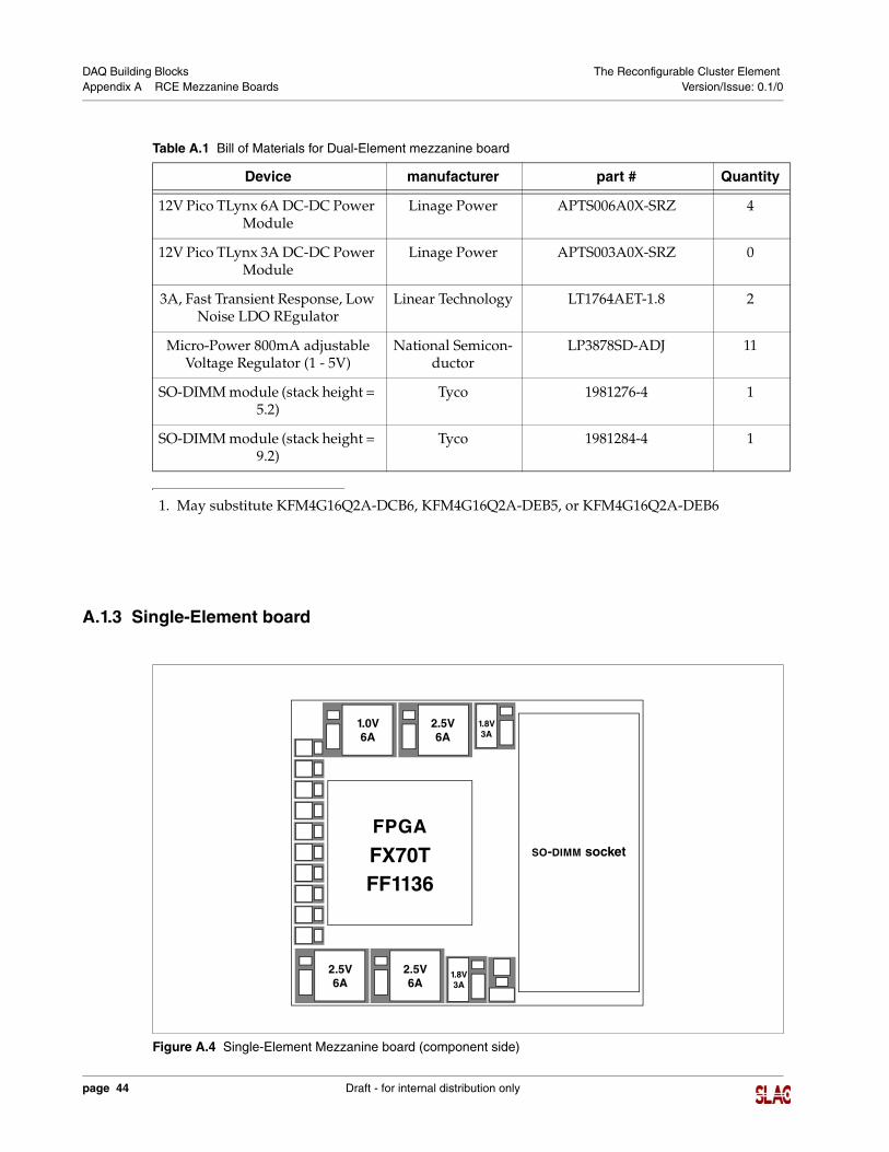
A.1.3 Single-Element board
Figure A.4 Single-Element Mezzanine board (component side)
SO-DIMM socket
FF1136
FPGA
FX70T
2.5V 2.5V
1.0V 2.5V
1.0V
1.2
1.2
1.2
1.2
1.0
1.0
1.0
1.0
1.8V3A
1.8V3A6A6A
6A 6A
12V Pico TLynx 6A DC-DC Power Module
Linage Power APTS006A0X-SRZ 4
12V Pico TLynx 3A DC-DC Power Module
Linage Power APTS003A0X-SRZ 0
3A, Fast Transient Response, Low Noise LDO REgulator
Linear Technology LT1764AET-1.8 2
Micro-Power 800mA adjustable Voltage Regulator (1 - 5V)
National Semicon-ductor
LP3878SD-ADJ 11
SO-DIMM module (stack height = 5.2)
Tyco 1981276-4 1
SO-DIMM module (stack height = 9.2)
Tyco 1981284-4 1
1. May substitute KFM4G16Q2A-DCB6, KFM4G16Q2A-DEB5, or KFM4G16Q2A-DEB6
Table A.1 Bill of Materials for Dual-Element mezzanine board
Device manufacturer part # Quantity
page 44 Draft - for internal distribution only
DAQ Building Blocks The Reconfigurable Cluster Element Appendix A RCE Mezzanine Boards Version/Issue: 0.1/0
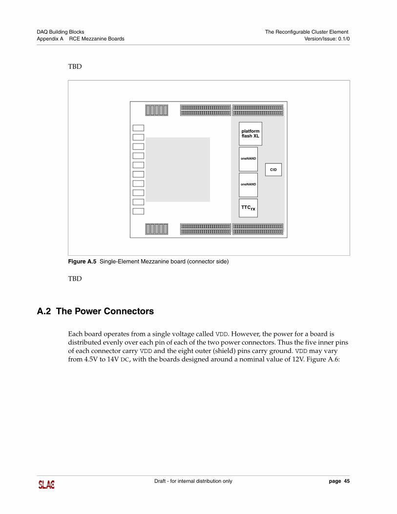
Figure A.5 Single-Element Mezzanine board (connector side)
TTCrx
platformflash XL
oneNAND
oneNAND
CID
TBD
TBD
A.2 The Power Connectors
Each board operates from a single voltage called VDD. However, the power for a board is distributed evenly over each pin of each of the two power connectors. Thus the five inner pins of each connector carry VDD and the eight outer (shield) pins carry ground. VDD may vary from 4.5V to 14V DC, with the boards designed around a nominal value of 12V. Figure A.6:
Draft - for internal distribution only page 45
DAQ Building Blocks The Reconfigurable Cluster Element Appendix A RCE Mezzanine Boards Version/Issue: 0.1/0
Figure A.6 Mapping of power and ground to a Power Connector
Power (VDD)
Ground (GND)
TBD
A.3 The A-Signal connectors
Figure A.7 Mapping of interface signals to the A-Signal connectors
BSI
HKI
JTAG
PRGM
GPIO
1
2 3 4 5 6 7
2
251 8 9 212223 2410 1112 13 141516 1718 1920
NRDY
XAUITRANSMIT
RECEIVE
12
LIO
ETC
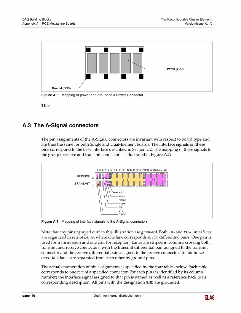
The pin assignments of the A-Signal connectors are invariant with respect to board type and are thus the same for both Single and Dual-Element boards. The interface signals on these pins correspond to the Base interface described in Section 2.2. The mapping of these signals to the group’s receive and transmit connectors is illustrated in Figure A.7:
Note that any pins “grayed out” in this illustration are grounded. Both LIO and XUAI interfaces are organized in sets of Lanes, where one lane corresponds to two differential pairs. One pair is used for transmission and one pair for reception. Lanes are striped in columns crossing both transmit and receive connectors, with the transmit differential pair assigned to the transmit connector and the receive differential pair assigned to the receive connector. To minimize cross-talk lanes are separated from each other by ground pins.
The actual enumeration of pin assignments is specified by the four tables below. Each table corresponds to one row of a specified connector. For each pin (as identified by its column number) the interface signal assigned to that pin is named as well as a reference back to its corresponding description. All pins with the designation GND are grounded.
page 46 Draft - for internal distribution only
DAQ Building Blocks The Reconfigurable Cluster Element Appendix A RCE Mezzanine Boards Version/Issue: 0.1/0
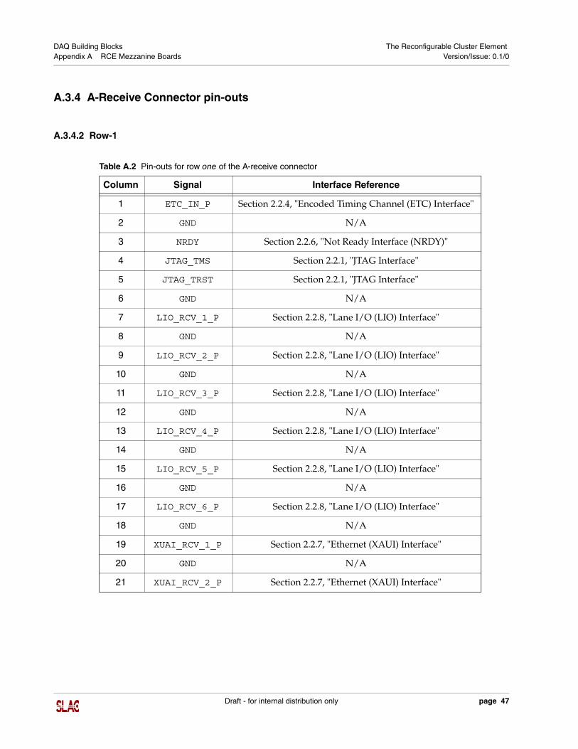
A.3.4 A-Receive Connector pin-outs
A.3.4.2 Row-1
Table A.2 Pin-outs for row one of the A-receive connector
Column Signal Interface Reference
1 ETC_IN_P Section 2.2.4, "Encoded Timing Channel (ETC) Interface"
2 GND N/A
3 NRDY Section 2.2.6, "Not Ready Interface (NRDY)"
4 JTAG_TMS Section 2.2.1, "JTAG Interface"
5 JTAG_TRST Section 2.2.1, "JTAG Interface"
6 GND N/A
7 LIO_RCV_1_P Section 2.2.8, "Lane I/O (LIO) Interface"
8 GND N/A
9 LIO_RCV_2_P Section 2.2.8, "Lane I/O (LIO) Interface"
10 GND N/A
11 LIO_RCV_3_P Section 2.2.8, "Lane I/O (LIO) Interface"
12 GND N/A
13 LIO_RCV_4_P Section 2.2.8, "Lane I/O (LIO) Interface"
14 GND N/A
15 LIO_RCV_5_P Section 2.2.8, "Lane I/O (LIO) Interface"
16 GND N/A
17 LIO_RCV_6_P Section 2.2.8, "Lane I/O (LIO) Interface"
18 GND N/A
19 XUAI_RCV_1_P Section 2.2.7, "Ethernet (XAUI) Interface"
20 GND N/A
21 XUAI_RCV_2_P Section 2.2.7, "Ethernet (XAUI) Interface"
Draft - for internal distribution only page 47
DAQ Building Blocks The Reconfigurable Cluster Element Appendix A RCE Mezzanine Boards Version/Issue: 0.1/0
A.3.4.3 Row-2
22 GND N/A
23 XUAI_RCV_3_P Section 2.2.7, "Ethernet (XAUI) Interface"
24 GND N/A
25 XUAI_RCV_4_P Section 2.2.7, "Ethernet (XAUI) Interface"
Table A.2 Pin-outs for row one of the A-receive connector
Column Signal Interface Reference
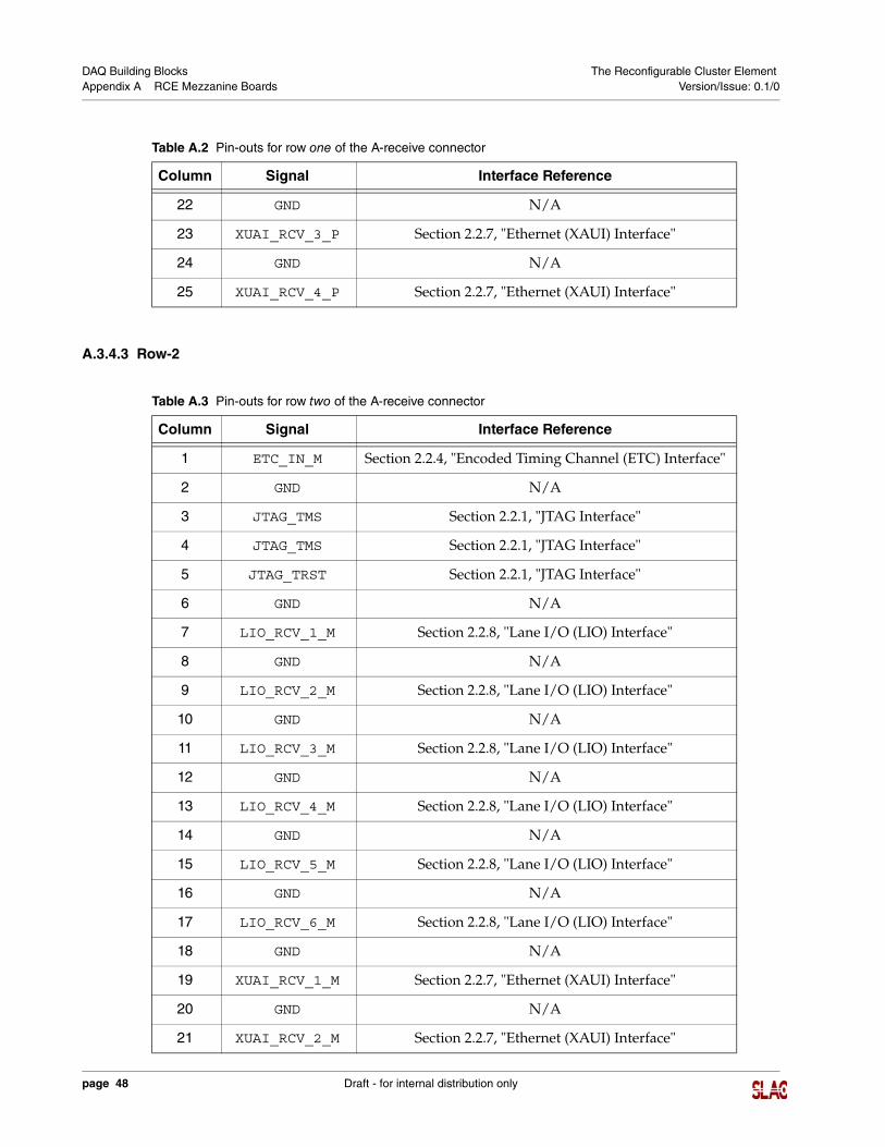
Table A.3 Pin-outs for row two of the A-receive connector
Column Signal Interface Reference
1 ETC_IN_M Section 2.2.4, "Encoded Timing Channel (ETC) Interface"
2 GND N/A
3 JTAG_TMS Section 2.2.1, "JTAG Interface"
4 JTAG_TMS Section 2.2.1, "JTAG Interface"
5 JTAG_TRST Section 2.2.1, "JTAG Interface"
6 GND N/A
7 LIO_RCV_1_M Section 2.2.8, "Lane I/O (LIO) Interface"
8 GND N/A
9 LIO_RCV_2_M Section 2.2.8, "Lane I/O (LIO) Interface"
10 GND N/A
11 LIO_RCV_3_M Section 2.2.8, "Lane I/O (LIO) Interface"
12 GND N/A
13 LIO_RCV_4_M Section 2.2.8, "Lane I/O (LIO) Interface"
14 GND N/A
15 LIO_RCV_5_M Section 2.2.8, "Lane I/O (LIO) Interface"
16 GND N/A
17 LIO_RCV_6_M Section 2.2.8, "Lane I/O (LIO) Interface"
18 GND N/A
19 XUAI_RCV_1_M Section 2.2.7, "Ethernet (XAUI) Interface"
20 GND N/A
21 XUAI_RCV_2_M Section 2.2.7, "Ethernet (XAUI) Interface"
page 48 Draft - for internal distribution only
DAQ Building Blocks The Reconfigurable Cluster Element Appendix A RCE Mezzanine Boards Version/Issue: 0.1/0
A.3.5 A-Transmit Connector pin-outs
A.3.5.4 Row-1
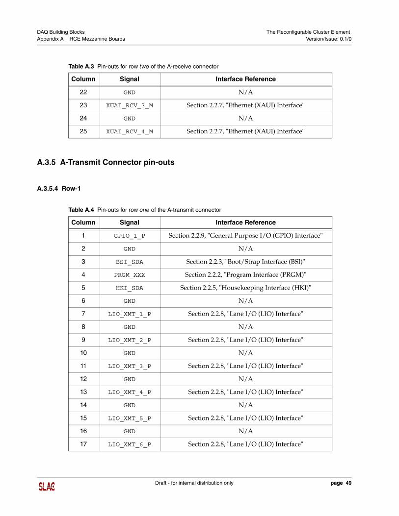
22 GND N/A
23 XUAI_RCV_3_M Section 2.2.7, "Ethernet (XAUI) Interface"
24 GND N/A
25 XUAI_RCV_4_M Section 2.2.7, "Ethernet (XAUI) Interface"
Table A.3 Pin-outs for row two of the A-receive connector
Column Signal Interface Reference
Table A.4 Pin-outs for row one of the A-transmit connector
Column Signal Interface Reference
1 GPIO_1_P Section 2.2.9, "General Purpose I/O (GPIO) Interface"
2 GND N/A
3 BSI_SDA Section 2.2.3, "Boot/Strap Interface (BSI)"
4 PRGM_XXX Section 2.2.2, "Program Interface (PRGM)"
5 HKI_SDA Section 2.2.5, "Housekeeping Interface (HKI)"
6 GND N/A
7 LIO_XMT_1_P Section 2.2.8, "Lane I/O (LIO) Interface"
8 GND N/A
9 LIO_XMT_2_P Section 2.2.8, "Lane I/O (LIO) Interface"
10 GND N/A
11 LIO_XMT_3_P Section 2.2.8, "Lane I/O (LIO) Interface"
12 GND N/A
13 LIO_XMT_4_P Section 2.2.8, "Lane I/O (LIO) Interface"
14 GND N/A
15 LIO_XMT_5_P Section 2.2.8, "Lane I/O (LIO) Interface"
16 GND N/A
17 LIO_XMT_6_P Section 2.2.8, "Lane I/O (LIO) Interface"
Draft - for internal distribution only page 49
DAQ Building Blocks The Reconfigurable Cluster Element Appendix A RCE Mezzanine Boards Version/Issue: 0.1/0
A.3.5.5 Row-2
18 GND N/A
19 XUAI_XMT_1_P Section 2.2.7, "Ethernet (XAUI) Interface"
20 GND N/A
21 XUAI_XMT_2_P Section 2.2.7, "Ethernet (XAUI) Interface"
22 GND N/A
23 XUAI_XMT_3_P Section 2.2.7, "Ethernet (XAUI) Interface"
24 GND N/A
25 XUAI_XMT_4_P Section 2.2.7, "Ethernet (XAUI) Interface"
Table A.4 Pin-outs for row one of the A-transmit connector
Column Signal Interface Reference
Table A.5 Pin-outs for row two of the A-transmit connector
Column Signal Interface Reference
1 GPIO_1_M Section 2.2.9, "General Purpose I/O (GPIO) Interface"
2 GND N/A
3 BSI_SCL Section 2.2.3, "Boot/Strap Interface (BSI)"
4 PRGM_XXX Section 2.2.2, "Program Interface (PRGM)"
5 HKI_SCL Section 2.2.5, "Housekeeping Interface (HKI)"
6 GND N/A
7 LIO_XMT_1_M Section 2.2.8, "Lane I/O (LIO) Interface"
8 GND N/A
9 LIO_XMT_2_M Section 2.2.8, "Lane I/O (LIO) Interface"
10 GND N/A
11 LIO_XMT_3_M Section 2.2.8, "Lane I/O (LIO) Interface"
12 GND N/A
13 LIO_XMT_4_M Section 2.2.8, "Lane I/O (LIO) Interface"
14 GND N/A
15 LIO_XMT_5_M Section 2.2.8, "Lane I/O (LIO) Interface"
16 GND N/A
17 LIO_XMT_6_M Section 2.2.8, "Lane I/O (LIO) Interface"
page 50 Draft - for internal distribution only
DAQ Building Blocks The Reconfigurable Cluster Element Appendix A RCE Mezzanine Boards Version/Issue: 0.1/0
A.4 The Connectors for the Dual-Element board
Figure A.8 Mapping of the interface signals to the Dual-Element Connectors
LIO
HKIB
XAUI 12
12RSVD
RSVD
GPIO
BSI
HKI
JTAG
PRGM
GPIO
1
2 3 4 5 6 7
2
251 8 9 212223 2410 1112 13 141516 1718 1920
NRDY
XAUITRANSMIT
RECEIVE
12
LIO
ETC
23456725 18921222324 1011121314151617181920
B-ConnectorsA-Connectors
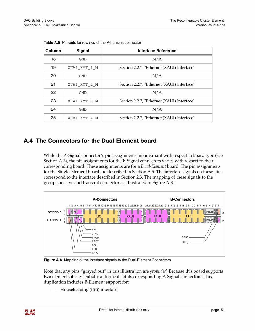
While the A-Signal connector’s pin assignments are invariant with respect to board type (see Section A.3), the pin assignments for the B-Signal connectors varies with respect to their corresponding board. These assignments are for a Dual-Element board. The pin assignments for the Single-Element board are described in Section A.5. The interface signals on these pins correspond to the interface described in Section 2.3. The mapping of these signals to the group’s receive and transmit connectors is illustrated in Figure A.8:
Note that any pins “grayed out” in this illustration are grounded. Because this board supports two elements it is essentially a duplicate of its corresponding A-Signal connectors. This duplication includes B-Element support for:
— Housekeeping (HKI) interface
18 GND N/A
19 XUAI_XMT_1_M Section 2.2.7, "Ethernet (XAUI) Interface"
20 GND N/A
21 XUAI_XMT_2_M Section 2.2.7, "Ethernet (XAUI) Interface"
22 GND N/A
23 XUAI_XMT_3_M Section 2.2.7, "Ethernet (XAUI) Interface"
24 GND N/A
25 XUAI_XMT_4_M Section 2.2.7, "Ethernet (XAUI) Interface"
Table A.5 Pin-outs for row two of the A-transmit connector
Column Signal Interface Reference
Draft - for internal distribution only page 51
DAQ Building Blocks The Reconfigurable Cluster Element Appendix A RCE Mezzanine Boards Version/Issue: 0.1/0
— Ethernet (XAUI) interface
— Lane I/O (LIO) interface
Both LIO and XUAI interfaces are organized in sets of Lanes, where one lane corresponds to two differential pairs. One pair is used for transmission and one pair for reception. Lanes are striped in columns crossing both transmit and receive connectors, with the transmit differential pair assigned to the transmit connector and the receive differential pair assigned to the receive connector. To minimize cross-talk lanes are separated from each other by ground pins.
The actual enumeration of pin assignments is specified by the four tables below. Each table corresponds to one row of a specified connector. For each pin (as identified by its column number) the interface signal assigned to that pin is named as well as a reference back to its corresponding description. All pins with the designation GND are grounded.
A.4.6 B-Receive Connector pin-outs
A.4.6.6 Row-1
Table A.6 Pin-outs for the Dual-element’s row one B-receive connector
Column Signal Interface Reference
1 GPIO_2_P Section 2.3.4, "More General Purpose I/O (GPIO)"
2 GND N/A
3 RSVD_1_P Section 2.3.5, "Reserved Signals (RSVD)"
4 RSVD_2_P Section 2.3.5, "Reserved Signals (RSVD)"
5 RSVD_3_P Section 2.3.5, "Reserved Signals (RSVD)"
6 GND N/A
7 B_LIO_RCV_1_P Section 2.3.3, "Second Lane I/O (LIO) Interface"
8 GND N/A
9 B_LIO_RCV_2_P Section 2.3.3, "Second Lane I/O (LIO) Interface"
10 GND N/A
11 B_LIO_RCV_3_P Section 2.3.3, "Second Lane I/O (LIO) Interface"
12 GND N/A
13 B_LIO_RCV_4_P Section 2.3.3, "Second Lane I/O (LIO) Interface"
14 GND N/A
15 B_LIO_RCV_5_P Section 2.3.3, "Second Lane I/O (LIO) Interface"
page 52 Draft - for internal distribution only
DAQ Building Blocks The Reconfigurable Cluster Element Appendix A RCE Mezzanine Boards Version/Issue: 0.1/0
A.4.6.7 Row-2
16 GND N/A
17 B_LIO_RCV_6_P Section 2.3.3, "Second Lane I/O (LIO) Interface"
18 GND N/A
19 B_XUAI_RCV_1_P Section 2.3.2, "Second Ethernet (XAUI) Interface"
20 GND N/A
21 B_XUAI_RCV_2_P Section 2.3.2, "Second Ethernet (XAUI) Interface"
22 GND N/A
23 B_XUAI_RCV_3_P Section 2.3.2, "Second Ethernet (XAUI) Interface"
24 GND N/A
25 B_XUAI_RCV_4_P Section 2.3.2, "Second Ethernet (XAUI) Interface"
Table A.6 Pin-outs for the Dual-element’s row one B-receive connector
Column Signal Interface Reference
Table A.7 Pin-outs for the Dual-element’s row two B-receive connector
Column Signal Interface Reference
1 GPIO_2_M Section 2.3.4, "More General Purpose I/O (GPIO)"
2 GND N/A
3 RSVD_1_M Section 2.3.5, "Reserved Signals (RSVD)"
4 RSVD_2_M Section 2.3.5, "Reserved Signals (RSVD)"
5 RSVD_3_M Section 2.3.5, "Reserved Signals (RSVD)"
6 GND N/A
7 B_LIO_RCV_1_M Section 2.3.3, "Second Lane I/O (LIO) Interface"
8 GND N/A
9 B_LIO_RCV_2_M Section 2.3.3, "Second Lane I/O (LIO) Interface"
10 GND N/A
11 B_LIO_RCV_3_M Section 2.3.3, "Second Lane I/O (LIO) Interface"
12 GND N/A
13 B_LIO_RCV_4_M Section 2.3.3, "Second Lane I/O (LIO) Interface"
Draft - for internal distribution only page 53
DAQ Building Blocks The Reconfigurable Cluster Element Appendix A RCE Mezzanine Boards Version/Issue: 0.1/0
A.4.7 B-Transmit Connector pin-outs
A.4.7.8 Row-1
14 GND N/A
15 B_LIO_RCV_5_M Section 2.3.3, "Second Lane I/O (LIO) Interface"
16 GND N/A
17 B_LIO_RCV_6_M Section 2.3.3, "Second Lane I/O (LIO) Interface"
18 GND N/A
19 B_XUAI_RCV_1_M Section 2.3.2, "Second Ethernet (XAUI) Interface"
20 GND N/A
21 B_XUAI_RCV_2_M Section 2.3.2, "Second Ethernet (XAUI) Interface"
22 GND N/A
23 B_XUAI_RCV_3_M Section 2.3.2, "Second Ethernet (XAUI) Interface"
24 GND N/A
25 B_XUAI_RCV_4_M Section 2.3.2, "Second Ethernet (XAUI) Interface"
Table A.7 Pin-outs for the Dual-element’s row two B-receive connector
Column Signal Interface Reference
Table A.8 Pin-outs for the Dual-element’s row one B-transmit connector
Column Signal Interface Reference
1 B_HKI_SDA Section 2.3.1, "Second Housekeeping Interface (HKI)"
2 GND N/A
3 RSVD_3_P Section 2.3.5, "Reserved Signals (RSVD)"
4 RSVD_4_P Section 2.3.5, "Reserved Signals (RSVD)"
5 RSVD_5_P Section 2.3.5, "Reserved Signals (RSVD)"
6 GND N/A
7 B_LIO_XMT_1_P Section 2.3.3, "Second Lane I/O (LIO) Interface"
8 GND N/A
9 B_LIO_XMT_2_P Section 2.3.3, "Second Lane I/O (LIO) Interface"
10 GND N/A
page 54 Draft - for internal distribution only
DAQ Building Blocks The Reconfigurable Cluster Element Appendix A RCE Mezzanine Boards Version/Issue: 0.1/0
A.4.7.9 Row-2
11 B_LIO_XMT_3_P Section 2.3.3, "Second Lane I/O (LIO) Interface"
12 GND N/A
13 B_LIO_XMT_4_P Section 2.3.3, "Second Lane I/O (LIO) Interface"
14 GND N/A
15 B_LIO_XMT_5_P Section 2.3.3, "Second Lane I/O (LIO) Interface"
16 GND N/A
17 B_LIO_XMT_6_P Section 2.3.3, "Second Lane I/O (LIO) Interface"
18 GND N/A
19 B_XUAI_XMT_1_P Section 2.3.2, "Second Ethernet (XAUI) Interface"
20 GND N/A
21 B_XUAI_XMT_2_P Section 2.3.2, "Second Ethernet (XAUI) Interface"
22 GND N/A
23 B_XUAI_XMT_3_P Section 2.3.2, "Second Ethernet (XAUI) Interface"
24 GND N/A
25 B_XUAI_XMT_4_P Section 2.3.2, "Second Ethernet (XAUI) Interface"
Table A.8 Pin-outs for the Dual-element’s row one B-transmit connector
Column Signal Interface Reference
Table A.9 Pin-outs for the Dual-element’s row one B-transmit connector
Column Signal Interface Reference
1 B_HKI_SCL Section 2.3.1, "Second Housekeeping Interface (HKI)"
2 GND N/A
3 RSVD_3_M Section 2.3.5, "Reserved Signals (RSVD)"
4 RSVD_4_M Section 2.3.5, "Reserved Signals (RSVD)"
5 RSVD_5_M Section 2.3.5, "Reserved Signals (RSVD)"
6 GND N/A
7 B_LIO_XMT_1_M Section 2.3.3, "Second Lane I/O (LIO) Interface"
8 GND N/A
Draft - for internal distribution only page 55
DAQ Building Blocks The Reconfigurable Cluster Element Appendix A RCE Mezzanine Boards Version/Issue: 0.1/0
A.5 The Connectors for the Single-Element board
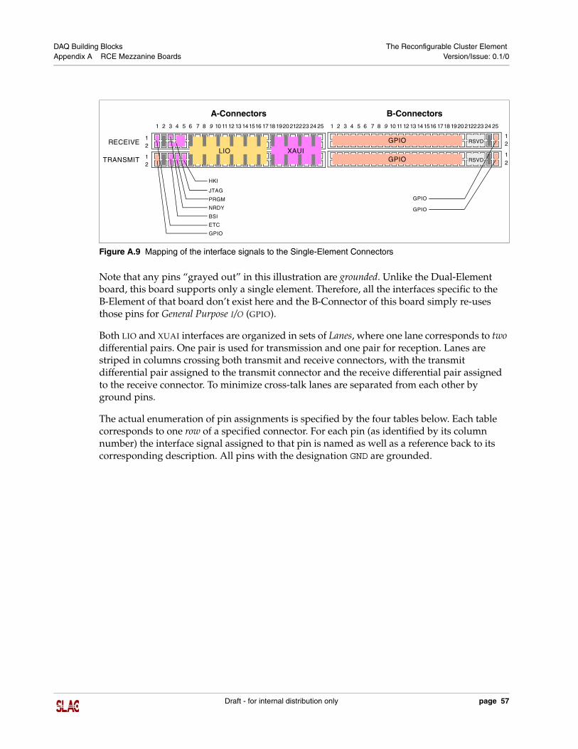
While the A-Signal connector’s pin assignments are invariant with respect to board type (see Section A.3), the pin assignments for the B-Signal connectors varies with respect to their corresponding board. These assignments are for a Single-Element board. The pin assignments for the Dual-Element board are described in Section A.4. The interface signals on these B-Connector’s pins correspond to the interface described in Section 2.4. The mapping of these signals to the group’s receive and transmit connectors is illustrated in Figure A.9:
9 B_LIO_XMT_2_M Section 2.3.3, "Second Lane I/O (LIO) Interface"
10 GND N/A
11 B_LIO_XMT_3_M Section 2.3.3, "Second Lane I/O (LIO) Interface"
12 GND N/A
13 B_LIO_XMT_4_M Section 2.3.3, "Second Lane I/O (LIO) Interface"
14 GND N/A
15 B_LIO_XMT_5_M Section 2.3.3, "Second Lane I/O (LIO) Interface"
16 GND N/A
17 B_LIO_XMT_6_M Section 2.3.3, "Second Lane I/O (LIO) Interface"
18 GND N/A
19 B_XUAI_XMT_1_M Section 2.3.2, "Second Ethernet (XAUI) Interface"
20 GND N/A
21 B_XUAI_XMT_2_M Section 2.3.2, "Second Ethernet (XAUI) Interface"
22 GND N/A
23 B_XUAI_XMT_3_M Section 2.3.2, "Second Ethernet (XAUI) Interface"
24 GND N/A
25 B_XUAI_XMT_4_M Section 2.3.2, "Second Ethernet (XAUI) Interface"
Table A.9 Pin-outs for the Dual-element’s row one B-transmit connector
Column Signal Interface Reference
page 56 Draft - for internal distribution only
DAQ Building Blocks The Reconfigurable Cluster Element Appendix A RCE Mezzanine Boards Version/Issue: 0.1/0
Figure A.9 Mapping of the interface signals to the Single-Element Connectors
GPIO
GPIO
12
12RSVD
RSVD
GPIO
GPIO
B-Connectors
BSI
HKI
JTAG
PRGM
GPIO
1
2 3 4 5 6 7
2
251 8 9 212223 2410 1112 13 141516 1718 1920
NRDY
XAUITRANSMIT
RECEIVE
12
LIO
ETC
2 3 4 5 6 7 251 8 9 212223 2410 1112 13 141516 1718 1920
A-Connectors
Note that any pins “grayed out” in this illustration are grounded. Unlike the Dual-Element board, this board supports only a single element. Therefore, all the interfaces specific to the B-Element of that board don’t exist here and the B-Connector of this board simply re-uses those pins for General Purpose I/O (GPIO).
Both LIO and XUAI interfaces are organized in sets of Lanes, where one lane corresponds to two differential pairs. One pair is used for transmission and one pair for reception. Lanes are striped in columns crossing both transmit and receive connectors, with the transmit differential pair assigned to the transmit connector and the receive differential pair assigned to the receive connector. To minimize cross-talk lanes are separated from each other by ground pins.
The actual enumeration of pin assignments is specified by the four tables below. Each table corresponds to one row of a specified connector. For each pin (as identified by its column number) the interface signal assigned to that pin is named as well as a reference back to its corresponding description. All pins with the designation GND are grounded.
Draft - for internal distribution only page 57
DAQ Building Blocks The Reconfigurable Cluster Element Appendix A RCE Mezzanine Boards Version/Issue: 0.1/0
A.5.8 B-Receive Connector pin-outs
A.5.8.10 Row-1
Table A.10 Pin-outs for the Single-Element’s row one B-receive connector
Column Signal Interface Reference
1 GPIO_2_P Section 2.3.4, "More General Purpose I/O (GPIO)"
2 GND N/A
3 RSVD_1_P Section 2.3.5, "Reserved Signals (RSVD)"
4 RSVD_2_P Section 2.3.5, "Reserved Signals (RSVD)"
5 RSVD_3_P Section 2.3.5, "Reserved Signals (RSVD)"
6 GND N/A
7 GPIO_4_P Section 2.3.4, "More General Purpose I/O (GPIO)"
8 GPIO_5_P Section 2.3.4, "More General Purpose I/O (GPIO)"
9 GPIO_6_P Section 2.3.4, "More General Purpose I/O (GPIO)"
10 GPIO_7_P Section 2.3.4, "More General Purpose I/O (GPIO)"
11 GPIO_8_P Section 2.3.4, "More General Purpose I/O (GPIO)"
12 GPIO_9_P Section 2.3.4, "More General Purpose I/O (GPIO)"
13 GPIO_10_P Section 2.3.4, "More General Purpose I/O (GPIO)"
14 GPIO_11_P Section 2.3.4, "More General Purpose I/O (GPIO)"
15 GPIO_12_P Section 2.3.4, "More General Purpose I/O (GPIO)"
16 GPIO_13_P Section 2.3.4, "More General Purpose I/O (GPIO)"
17 GPIO_14_P Section 2.3.4, "More General Purpose I/O (GPIO)"
18 GPIO_15_P Section 2.3.4, "More General Purpose I/O (GPIO)"
19 GPIO_16_P Section 2.3.4, "More General Purpose I/O (GPIO)"
20 GPIO_17_P Section 2.3.4, "More General Purpose I/O (GPIO)"
21 GPIO_18_P Section 2.3.4, "More General Purpose I/O (GPIO)"
22 GPIO_19_P Section 2.3.4, "More General Purpose I/O (GPIO)"
23 GPIO_20_P Section 2.3.4, "More General Purpose I/O (GPIO)"
24 GPIO_21_P Section 2.3.4, "More General Purpose I/O (GPIO)"
25 GPIO_22_P Section 2.3.4, "More General Purpose I/O (GPIO)"
page 58 Draft - for internal distribution only

DAQ Building Blocks The Reconfigurable Cluster Element Appendix A RCE Mezzanine Boards Version/Issue: 0.1/0
A.5.8.11 Row-2
Table A.11 Pin-outs for the Single-Element’s row two B-receive connector
Column Signal Interface Reference
1 GPIO_2_M Section 2.3.4, "More General Purpose I/O (GPIO)"
2 GND N/A
3 RSVD_1_M Section 2.3.5, "Reserved Signals (RSVD)"
4 RSVD_2_M Section 2.3.5, "Reserved Signals (RSVD)"
5 RSVD_3_M Section 2.3.5, "Reserved Signals (RSVD)"
6 GND N/A
7 GPIO_4_M Section 2.3.4, "More General Purpose I/O (GPIO)"
8 GPIO_5_M Section 2.3.4, "More General Purpose I/O (GPIO)"
9 GPIO_6_M Section 2.3.4, "More General Purpose I/O (GPIO)"
10 GPIO_7_M Section 2.3.4, "More General Purpose I/O (GPIO)"
11 GPIO_8_M Section 2.3.4, "More General Purpose I/O (GPIO)"
12 GPIO_9_M Section 2.3.4, "More General Purpose I/O (GPIO)"
13 GPIO_10_M Section 2.3.4, "More General Purpose I/O (GPIO)"
14 GPIO_11_M Section 2.3.4, "More General Purpose I/O (GPIO)"
15 GPIO_12_M Section 2.3.4, "More General Purpose I/O (GPIO)"
16 GPIO_13_M Section 2.3.4, "More General Purpose I/O (GPIO)"
17 GPIO_14_M Section 2.3.4, "More General Purpose I/O (GPIO)"
18 GPIO_15_M Section 2.3.4, "More General Purpose I/O (GPIO)"
19 GPIO_16_M Section 2.3.4, "More General Purpose I/O (GPIO)"
20 GPIO_17_M Section 2.3.4, "More General Purpose I/O (GPIO)"
21 GPIO_18_M Section 2.3.4, "More General Purpose I/O (GPIO)"
22 GPIO_19_M Section 2.3.4, "More General Purpose I/O (GPIO)"
23 GPIO_20_M Section 2.3.4, "More General Purpose I/O (GPIO)"
24 GPIO_21_M Section 2.3.4, "More General Purpose I/O (GPIO)"
25 GPIO_22_M Section 2.3.4, "More General Purpose I/O (GPIO)"
Draft - for internal distribution only page 59
DAQ Building Blocks The Reconfigurable Cluster Element Appendix A RCE Mezzanine Boards Version/Issue: 0.1/0
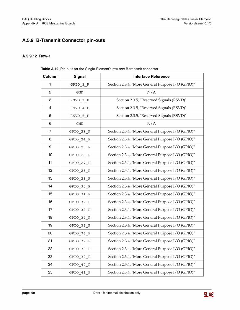
A.5.9 B-Transmit Connector pin-outs
A.5.9.12 Row-1
Table A.12 Pin-outs for the Single-Element’s row one B-transmit connector
Column Signal Interface Reference
1 GPIO_3_P Section 2.3.4, "More General Purpose I/O (GPIO)"
2 GND N/A
3 RSVD_3_P Section 2.3.5, "Reserved Signals (RSVD)"
4 RSVD_4_P Section 2.3.5, "Reserved Signals (RSVD)"
5 RSVD_5_P Section 2.3.5, "Reserved Signals (RSVD)"
6 GND N/A
7 GPIO_23_P Section 2.3.4, "More General Purpose I/O (GPIO)"
8 GPIO_24_P Section 2.3.4, "More General Purpose I/O (GPIO)"
9 GPIO_25_P Section 2.3.4, "More General Purpose I/O (GPIO)"
10 GPIO_26_P Section 2.3.4, "More General Purpose I/O (GPIO)"
11 GPIO_27_P Section 2.3.4, "More General Purpose I/O (GPIO)"
12 GPIO_28_P Section 2.3.4, "More General Purpose I/O (GPIO)"
13 GPIO_29_P Section 2.3.4, "More General Purpose I/O (GPIO)"
14 GPIO_30_P Section 2.3.4, "More General Purpose I/O (GPIO)"
15 GPIO_31_P Section 2.3.4, "More General Purpose I/O (GPIO)"
16 GPIO_32_P Section 2.3.4, "More General Purpose I/O (GPIO)"
17 GPIO_33_P Section 2.3.4, "More General Purpose I/O (GPIO)"
18 GPIO_34_P Section 2.3.4, "More General Purpose I/O (GPIO)"
19 GPIO_35_P Section 2.3.4, "More General Purpose I/O (GPIO)"
20 GPIO_36_P Section 2.3.4, "More General Purpose I/O (GPIO)"
21 GPIO_37_P Section 2.3.4, "More General Purpose I/O (GPIO)"
22 GPIO_38_P Section 2.3.4, "More General Purpose I/O (GPIO)"
23 GPIO_39_P Section 2.3.4, "More General Purpose I/O (GPIO)"
24 GPIO_40_P Section 2.3.4, "More General Purpose I/O (GPIO)"
25 GPIO_41_P Section 2.3.4, "More General Purpose I/O (GPIO)"
page 60 Draft - for internal distribution only
DAQ Building Blocks The Reconfigurable Cluster Element Appendix A RCE Mezzanine Boards Version/Issue: 0.1/0
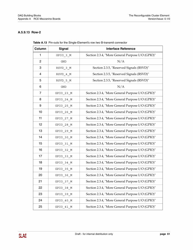
A.5.9.13 Row-2
Table A.13 Pin-outs for the Single-Element’s row two B-transmit connector
Column Signal Interface Reference
1 GPIO_3_M Section 2.3.4, "More General Purpose I/O (GPIO)"
2 GND N/A
3 RSVD_3_M Section 2.3.5, "Reserved Signals (RSVD)"
4 RSVD_4_M Section 2.3.5, "Reserved Signals (RSVD)"
5 RSVD_5_M Section 2.3.5, "Reserved Signals (RSVD)"
6 GND N/A
7 GPIO_23_M Section 2.3.4, "More General Purpose I/O (GPIO)"
8 GPIO_24_M Section 2.3.4, "More General Purpose I/O (GPIO)"
9 GPIO_25_M Section 2.3.4, "More General Purpose I/O (GPIO)"
10 GPIO_26_M Section 2.3.4, "More General Purpose I/O (GPIO)"
11 GPIO_27_M Section 2.3.4, "More General Purpose I/O (GPIO)"
12 GPIO_28_M Section 2.3.4, "More General Purpose I/O (GPIO)"
13 GPIO_29_M Section 2.3.4, "More General Purpose I/O (GPIO)"
14 GPIO_30_M Section 2.3.4, "More General Purpose I/O (GPIO)"
15 GPIO_31_M Section 2.3.4, "More General Purpose I/O (GPIO)"
16 GPIO_32_M Section 2.3.4, "More General Purpose I/O (GPIO)"
17 GPIO_33_M Section 2.3.4, "More General Purpose I/O (GPIO)"
18 GPIO_34_M Section 2.3.4, "More General Purpose I/O (GPIO)"
19 GPIO_35_M Section 2.3.4, "More General Purpose I/O (GPIO)"
20 GPIO_36_M Section 2.3.4, "More General Purpose I/O (GPIO)"
21 GPIO_37_M Section 2.3.4, "More General Purpose I/O (GPIO)"
22 GPIO_38_M Section 2.3.4, "More General Purpose I/O (GPIO)"
23 GPIO_39_M Section 2.3.4, "More General Purpose I/O (GPIO)"
24 GPIO_40_M Section 2.3.4, "More General Purpose I/O (GPIO)"
25 GPIO_41_M Section 2.3.4, "More General Purpose I/O (GPIO)"
Draft - for internal distribution only page 61
DAQ Building Blocks The Reconfigurable Cluster Element Appendix A RCE Mezzanine Boards Version/Issue: 0.1/0
page 62 Draft - for internal distribution only
DAQ Building Blocks The Reconfigurable Cluster Element Appendix B Gen I Mezzanine Board Version/Issue: 0.1/0
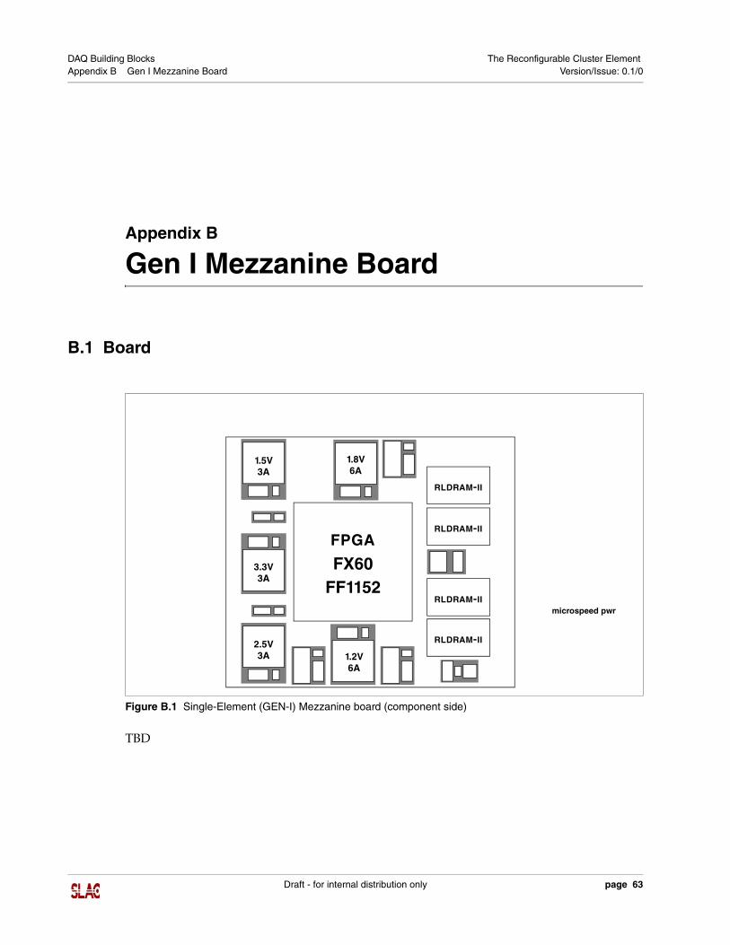
Appendix B Gen I Mezzanine Board
B.1 Board
Figure B.1 Single-Element (GEN-I) Mezzanine board (component side)
microspeed pwr
FF1152
FPGA
FX60
RLDRAM-II
RLDRAM-II
RLDRAM-II
RLDRAM-II
1.5V 1.8V
1.2V
3.3V
2.5V
3A 6A
3A
3A6A
TBD
Draft - for internal distribution only page 63
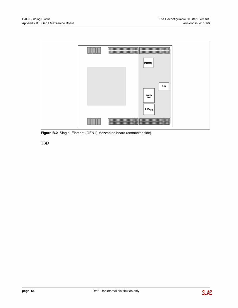
DAQ Building Blocks The Reconfigurable Cluster Element Appendix B Gen I Mezzanine Board Version/Issue: 0.1/0
Figure B.2 Single -Element (GEN-I) Mezzanine board (connector side)
TTCrx
PROM
config
CID
flash
TBD
page 64 Draft - for internal distribution only