term paper wide range tuning in cmos lc-vcoskphang/papers/2002/iahmed_lcosc.pdf · term paper: wide...
TRANSCRIPT
Term Paper: Wide range tuning in CMOS LC-VCOs By: Imran Ahmed MaSc. Candidate, Electronics Group Student number: 970836120 Date: November 15th, 2002
ECE1352F: Analog Circuits Professor Khoman Phang Edward S. Rogers Sr. Department of Electrical and Computer Engineering University of Toronto
Abstract This paper discusses various implementations of wide range frequency tuning for LC-VCOs in CMOS processes. It is shown that wide tuning ranges are required in certain applications to compensate for process variation, and in others to allow for wide locking ranges in PLLs. The discussion focuses on highlighting the key tradeoffs of power, phase noise, tuning range and area, with the illustration of different tuning techniques for RF/wireless and CDR type applications. Specifically it is shown that for RF/wireless applications, due to the stringent demands on minimal phase noise and power, a varactor based tuning scheme is necessary. For CDR applications it is shown that a relaxed constraint on power and phase noise allows the use of lossy-switched capacitor tuning to achieve very wide tuning ranges. Active inductor emulation is introduced as a means to maintain low power and wide tuning range with low area at the cost of increased phase noise. The discussion concludes with a brief look into where research in the field of wide range tuning in LC-VCOs is heading.
2

Table of Contents
1. Introduction ................................................................................................................. 4 2. Background Information .............................................................................................. 5
2.1 Phased Locked Loops ........................................................................................... 5 2.2 Conditions for oscillation in an LC oscillator .......................................................... 6 2.3 Tuning LC oscillators ............................................................................................. 8
2.3.1 Diode based varactor ...................................................................................... 8 2.3.2 Switched capacitor tuning ............................................................................... 9
3. Modern Tuning Implementations............................................................................... 11 3.1 RF/wireless applications ...................................................................................... 11 3.2 CDR structures .................................................................................................... 14 3.3 Active Inductors ................................................................................................... 17
4. Future directions........................................................................................................ 19 5. Conclusions............................................................................................................... 20 References:................................................................................................................... 21
3
1. Introduction
With the demand for high speed and wireless devices driving the electronics market, much
research has gone into developing faster circuits and improved semiconductor processing. In
recent years there has been a strong move to integrate entire systems on a single chip (SoC) so as
to yield compact and economical solutions. Circuit blocks that were previously designed using
discrete components, presently can be implemented monolithically on an integrated circuit. A
particular example of such a block, which is pervasive in high speed and wireless electronics, is
the inductor-capacitor based voltage controlled oscillator (LC-VCO). LC-VCOs are the
preferred method to generate high frequency clocks, as the LC-VCO is more immune to phase
noise than alternative VCO architectures (e.g. ring oscillators), hence is well suited for
applications that demand spectrally pure clocks at high frequencies, such as RF/wireless
applications, and high-speed Clock and Data Recovery (CDR) circuits.
Monolithic LC-VCOs do not come without their fair share of trade offs. In particular, it is
difficult to fabricate on-chip inductors with high Qs [1], subsequently requiring LC-VCOs to
consume much power to stabilize oscillations. Furthermore the variation in inductance and
capacitance due to process limitations can impart a large variation on the central frequency (~
±20% [1]). Thus to compensate for process variation, the oscillator frequency must be able to be
tuned by at least ±20%. Large variations in central frequency along with a desire to have a
tunable central frequency for certain applications (e.g. CDR) has prompted research on wide
range tuning techniques for LC-VCOs (i.e. greater than 20% tuning). Due to the sensitivity of
high frequency applications to power consumption, noise, and area the choice of which tuning
technique can be employed to is limited by application requirements. For example, LC-VCOs
for RF/wireless applications require low power consumption and phase noise, but often only
require 20-30% tuning range. CDR circuits for digital video however demands much wider tune
ability from the VCO (50%+), but can tolerate more noise and larger power consumption than
RF/wireless circuits.
This paper aims to introduce wide range tuning techniques for LC-VCOs, where specific
techniques are shown to achieve different compromises between power, phase noise, tuning
range and area.
4
2. Background Information
This section briefly introduces the context of a VCO within a PLL, followed by a discussion of
criteria necessary for oscillations to occur in LC oscillators, hence the trade-offs any tuning
scheme would face. Traditional frequency tuning schemes of varactors and switched capacitor
tuning are also presented, where the limitations of traditional schemes motivate current research
(the focus of section three).
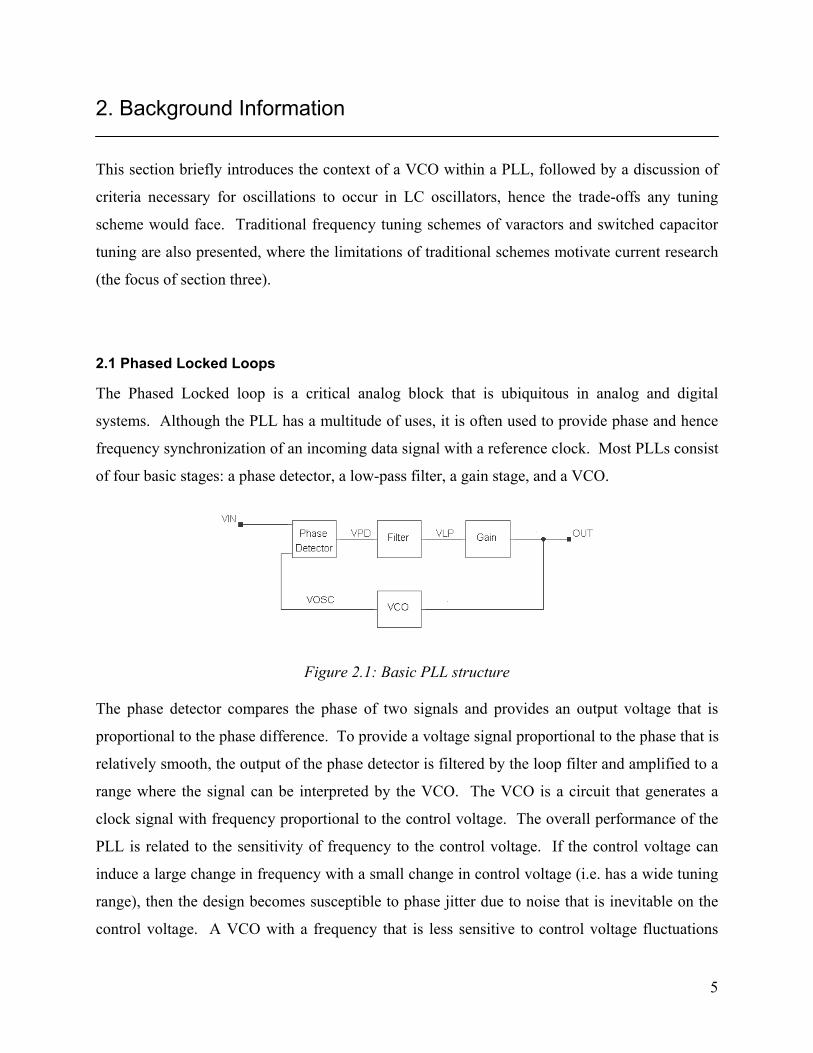
2.1 Phased Locked Loops
The Phased Locked loop is a critical analog block that is ubiquitous in analog and digital
systems. Although the PLL has a multitude of uses, it is often used to provide phase and hence
frequency synchronization of an incoming data signal with a reference clock. Most PLLs consist
of four basic stages: a phase detector, a low-pass filter, a gain stage, and a VCO.
Figure 2.1: Basic PLL structure
The phase detector compares the phase of two signals and provides an output voltage that is
proportional to the phase difference. To provide a voltage signal proportional to the phase that is
relatively smooth, the output of the phase detector is filtered by the loop filter and amplified to a
range where the signal can be interpreted by the VCO. The VCO is a circuit that generates a
clock signal with frequency proportional to the control voltage. The overall performance of the
PLL is related to the sensitivity of frequency to the control voltage. If the control voltage can
induce a large change in frequency with a small change in control voltage (i.e. has a wide tuning
range), then the design becomes susceptible to phase jitter due to noise that is inevitable on the
control voltage. A VCO with a frequency that is less sensitive to control voltage fluctuations
5
imparts less phase jitter to the system, but suffers from a narrower tuning range for a fixed power
supply. This is an important issue in the design of tuning mechanisms for LC-VCOs, and
solution to which is discussed in section 3.2. For further reference, a more detailed analysis of
PLL operation can be found in [2].
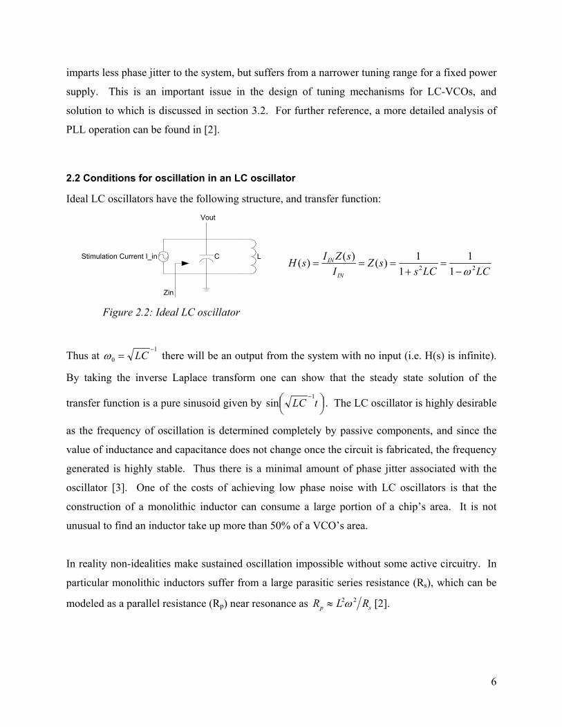
2.2 Conditions for oscillation in an LC oscillator
Ideal LC oscillators have the following structure, and transfer function:
LCStimulation Current I_in
Zin
Vout
Figure 2.2: Ideal LC oscillator
LCLCssZ
IsZIsH
IN
IN22 1
11
1)()()(ω−
=+
===
Thus at 1
0
−= LCω there will be an output from the system with no input (i.e. H(s) is infinite).
By taking the inverse Laplace transform one can show that the steady state solution of the
transfer function is a pure sinusoid given by
−
tLC1
sin . The LC oscillator is highly desirable
as the frequency of oscillation is determined completely by passive components, and since the
value of inductance and capacitance does not change once the circuit is fabricated, the frequency
generated is highly stable. Thus there is a minimal amount of phase jitter associated with the
oscillator [3]. One of the costs of achieving low phase noise with LC oscillators is that the
construction of a monolithic inductor can consume a large portion of a chip’s area. It is not
unusual to find an inductor take up more than 50% of a VCO’s area.
In reality non-idealities make sustained oscillation impossible without some active circuitry. In
particular monolithic inductors suffer from a large parasitic series resistance (Rs), which can be
modeled as a parallel resistance (Rp) near resonance as sp RLR 22ω≈ [2].
6
LC
Zin
Vout
Rp
Figure 2.3: Practical LC oscillator
The transfer function of the oscillator including
resistance thus becomes:
LCCRss
Cs
sH
p
1)(2 ++
=
The inverse Laplace transform of the above function is of a damped sinusoid with frequency 1
0
−≈ LCω for CLRp 5.0> . Thus without the aid of some external circuitry, output
oscillations will cease after a short period of time. If some form of negative resistance could be
used to load the oscillator, the lossy resistance could effectively be eliminated. Indeed this is
often what is done to sustain oscillations, where a negative resistance is formed by a cross-
coupled transistor pair (the cross-coupled resistor imparts –2/gm impedance to the circuit [2]).
Figure 2.4: View of an LC oscillator as a one port network, where energy restorer can be a
negative resistance
Cross coupled loadsform energyrestoration
Figure 2.5: Symmetric cross coupled loads to
impart negative resistance
Therefore the parallel combination of tank resistance and negative resistance is:
21
1m
p
gR −
7
The combination of negative and positive parallel resistance cancels for 1/Rp=gm/2, and is
infinite between the output and ground, i.e. oscillator appears ideal. The relation of gm to Rp to
sustain oscillations presents an important trade off that is critical to consider in tuning schemes.
Namely, if Rs is large, Rp is small, and hence gm is required to be large to sustain oscillations.
Since dm Ig ∝ , this implies that for an LC-oscillator system that is lossy (i.e. has a low Q,
where Q defines the ratio of reactance to resistance of a passive component), a large amount of
current hence power is required to stabilize the oscillation.
2.3 Tuning LC oscillators
From the discussion in section 2.2, it is clear that the frequency of oscillation is set by the value
of L and C. Thus to tune the frequency of an LC oscillator would require the dynamic
adjustment of either L or C. Since it is difficult to produce a tunable passive inductor, most
tuning schemes involve the use of an adjustable capacitor.
Traditionally adjustable capacitances are implemented in one of two ways: 1.) by a varactor or
2.) by a switched capacitor.
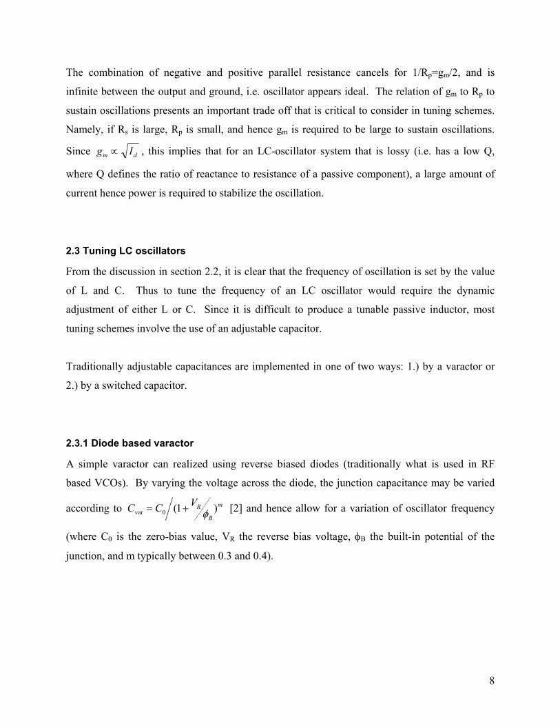
2.3.1 Diode based varactor
A simple varactor can realized using reverse biased diodes (traditionally what is used in RF
based VCOs). By varying the voltage across the diode, the junction capacitance may be varied
according to m
B
RVC )1(0var φ+=C [2] and hence allow for a variation of oscillator frequency
(where C0 is the zero-bias value, VR the reverse bias voltage, φB the built-in potential of the
junction, and m typically between 0.3 and 0.4).
8
VDD
VCNT
VOUT
Figure 2.6: Diode varactor to tune LC-VCO
Diode based varactors however suffer from two key drawbacks: 1.) A low Q, and 2.) A limited
tuning range. To impart only capacitive impedance, the diode varactors must stay in reverse
bias. Diodes however can near forward bias for fairly low control voltages. Near forward bias
the current increases exponentially, imparting a sizeable leakage current through the diode,
reducing the Q of the tunable capacitor (i.e. introduces a series resistance). As shown in section
2.2, this translates into an increased demand in power consumption to stabilize oscillations.
Furthermore as the introduction of a lossy resistance inherently introduces noise to the system,
the oscillator becomes more susceptible to phase variations [4]. Since a diode can become
forward biased for a small-applied voltage, the range of voltages that may be applied to a diode,
and hence range of junction capacitances is limited.
Most diode based tuning schemes can only achieve a tuning range of about ±10% [4]. In some
applications where the variation in central frequency is not critical, a ±10% tuning range is
sufficient. However in modern deep sub-micron RF/wireless circuits where bandwidth
allocation is extremely narrow, alternative methods of tuning need to be used to achieve a wider
tuning range to compensate process variations, while addressing RF/wireless system issues.
Such methods are described in section 3.1.
2.3.2 Switched capacitor tuning
Rather than using a varactor to achieve capacitive tuning, a wide range of capacitor values can be
achieved by activating capacitors in parallel with switches.
9

Switchedcapacitor tuning
Figure 2.7: Switched capacitor tuning
As there is no limitation on the value of capacitance that can be switched in, an effective ultra-
wide tuning range can be achieved with this approach. Note however that each switch, which is
implemented with an MOS pass transistor, introduces a finite resistance in series to the
capacitance it switches in. A switched capacitor tuning approach hence is inherently lossy and
suffers from a low Q. Thus stabilizing the oscillation requires a large consumption of power by
the negative impedance, as shown in section two. As a result it can be concluded that an ultra-
wide tuning range comes at the cost of both increased power and phase noise (due to low Q [3,
5]), hence limiting the applications to which this particular tuning technique may be used. Thus
to improve the viability of the switched tuning capacitor technique, current research has focused
on minimizing power consumption for such structures, and is the focus of section 3.2.
10
3. Modern Tuning Implementations
This section describes modern implementations of tuning schemes for LC-VCOs in RF/wireless
applications, and CDR circuits. These applications have been highlighted as they illustrate the
effects of different tuning techniques on oscillator performance, where in each application the
desired trade off is different due to the nature of the application.
3.1 RF/wireless applications
In RF based systems spectral purity is of prime importance. For example in Frequency Division
Multiplexed (FDM) based systems, if a VCO were to generate a clock that varied by ±20%, a
frequency demodulation operation could inadvertently demodulate an adjacent channel, rather
than the desired channel. In addition, modern RF based systems tend to be used in wireless
applications. As such to conserve battery power, it is critical to minimize power consumption. It
was noted in section two that low power and spectral purity came at the cost of reduced tuning
range, due to the low Q in switches used to achieve very wide tuning ranges. To satisfy the
critical power and noise constraints, RF/wireless based VCOs use the varactor approach to
achieve tuning [1]. Furthermore as the goal of tuning in RF circuits is primarily to compensate
for process variation, a tuning range of only ±20%+ is required. As a result of the restriction on
tuning technique, current research for RF LC-VCOs has sought to improve on the varactor
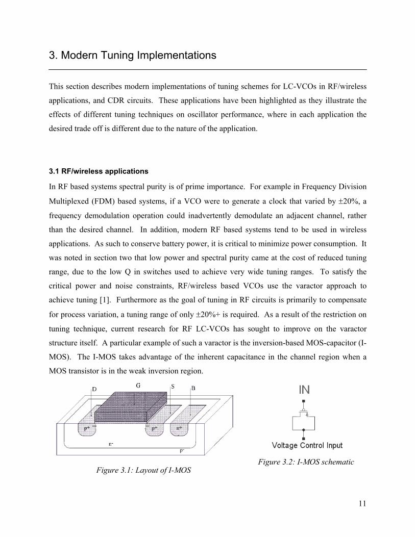
structure itself. A particular example of such a varactor is the inversion-based MOS-capacitor (I-
MOS). The I-MOS takes advantage of the inherent capacitance in the channel region when a
MOS transistor is in the weak inversion region.
Figure 3.1: Layout of I-MOS
Figure 3.2: I-MOS schematic
11

In a PMOS transistor, if the source and drain are tied together with the body terminal tied to VDD,
as the potential at the S/D regions increases, a channel region will form between the S/D
implants. Since in the weak region the channel is a poor conductor, it forms an effective
dielectric between the gate-oxide interface and substrate. The gate capacitance is hence
effectively given by a series combination of the capacitance due to the gate oxide and channel
regions, given by: chox
choxeff CC
CC+
=C . Since Cch is a function of Vsd, the effective gate capacitance
is modulated by Vsd, hence Ceff behaves as a varactor. As Vsd increases, the inversion channel
eventually penetrates to a fixed depth. At that point the effective gate capacitance saturates,
hence imposes a minimum capacitance. A typical tuning profile is given in figure 3.3.
Figure 3.3: Typical tuning range of I-MOS
Unlike the diode varactor, the control voltage for the I-MOS is capable of switching rail-rail
without imparting any deleterious effects upon the circuit; as such a wider variation of the
effective capacitance is possible. Furthermore, the series resistance due primarily to the effective
dielectric in the channel region is low enough that the noise figure (induced by the resistance and
power consumption to stabilize the circuit) is suitable for RF applications [1].
I-MOS caps used in LC-VCOs typically achieve ±20% tuning. Since the tuning range of ±20%
is often sufficient to cover process variation, they are often used as the tuning mechanism for
LC-VCOs in RF circuits.
12
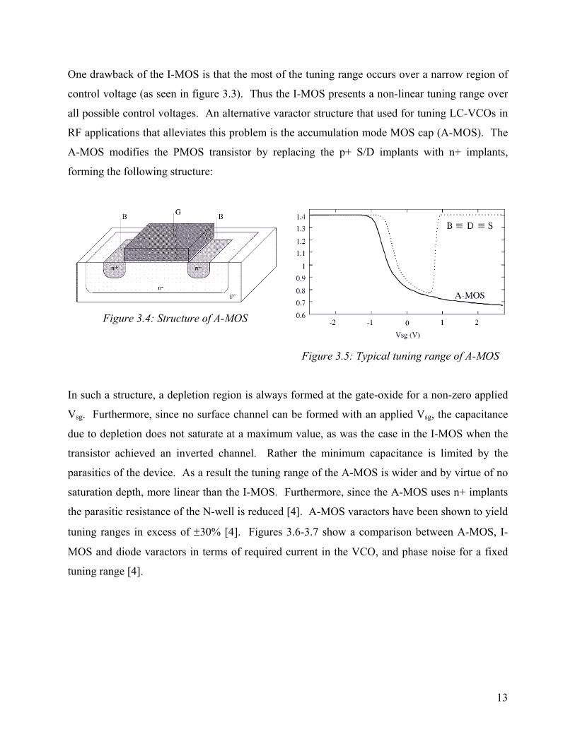
One drawback of the I-MOS is that the most of the tuning range occurs over a narrow region of
control voltage (as seen in figure 3.3). Thus the I-MOS presents a non-linear tuning range over
all possible control voltages. An alternative varactor structure that used for tuning LC-VCOs in
RF applications that alleviates this problem is the accumulation mode MOS cap (A-MOS). The
A-MOS modifies the PMOS transistor by replacing the p+ S/D implants with n+ implants,
forming the following structure:
Figure 3.4: Structure of A-MOS
Figure 3.5: Typical tuning range of A-MOS
In such a structure, a depletion region is always formed at the gate-oxide for a non-zero applied
Vsg. Furthermore, since no surface channel can be formed with an applied Vsg, the capacitance
due to depletion does not saturate at a maximum value, as was the case in the I-MOS when the
transistor achieved an inverted channel. Rather the minimum capacitance is limited by the
parasitics of the device. As a result the tuning range of the A-MOS is wider and by virtue of no
saturation depth, more linear than the I-MOS. Furthermore, since the A-MOS uses n+ implants
the parasitic resistance of the N-well is reduced [4]. A-MOS varactors have been shown to yield
tuning ranges in excess of ±30% [4]. Figures 3.6-3.7 show a comparison between A-MOS, I-
MOS and diode varactors in terms of required current in the VCO, and phase noise for a fixed
tuning range [4].
13
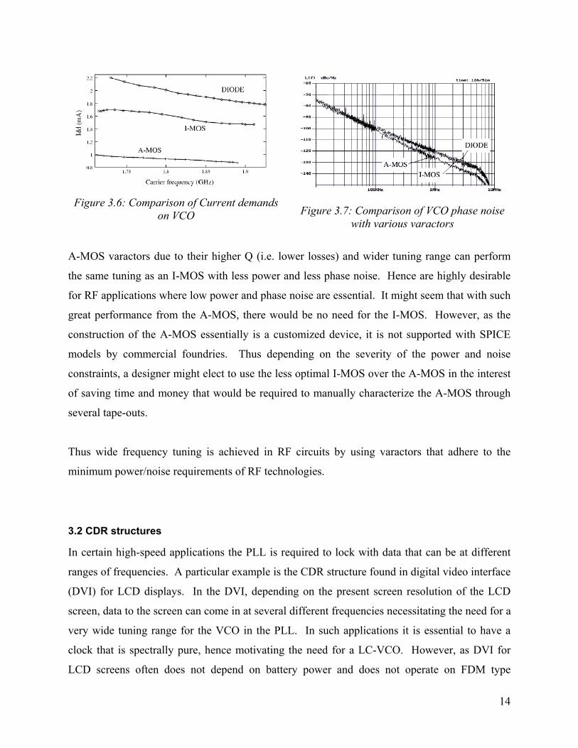
Figure 3.6: Comparison of Current demands
on VCO
Figure 3.7: Comparison of VCO phase noise
with various varactors
A-MOS varactors due to their higher Q (i.e. lower losses) and wider tuning range can perform
the same tuning as an I-MOS with less power and less phase noise. Hence are highly desirable
for RF applications where low power and phase noise are essential. It might seem that with such
great performance from the A-MOS, there would be no need for the I-MOS. However, as the
construction of the A-MOS essentially is a customized device, it is not supported with SPICE
models by commercial foundries. Thus depending on the severity of the power and noise
constraints, a designer might elect to use the less optimal I-MOS over the A-MOS in the interest
of saving time and money that would be required to manually characterize the A-MOS through
several tape-outs.
Thus wide frequency tuning is achieved in RF circuits by using varactors that adhere to the
minimum power/noise requirements of RF technologies.
3.2 CDR structures
In certain high-speed applications the PLL is required to lock with data that can be at different
ranges of frequencies. A particular example is the CDR structure found in digital video interface
(DVI) for LCD displays. In the DVI, depending on the present screen resolution of the LCD
screen, data to the screen can come in at several different frequencies necessitating the need for a
very wide tuning range for the VCO in the PLL. In such applications it is essential to have a
clock that is spectrally pure, hence motivating the need for a LC-VCO. However, as DVI for
LCD screens often does not depend on battery power and does not operate on FDM type
14
concepts, the stringent requirements of phase noise and power are more relaxed than RF
applications. As such, these parameters can be traded off, yielding a different approach to solve
the tuning range problem.
Since power and phase noise may be traded off, it is possible to introduce additional resistance
into the VCO tank. In particular we note that if transistor based switches are used to switch
capacitors in parallel with the inductor, the effective tank capacitance can be digitally controlled.
Since the switches can be used to switch in arbitrary fixed capacitances, the effective tuning
range can be very large (see figure 2.7 in section 2.3.2)
As a PLL requires a continuous tuning range from the VCO, the switched capacitors would have
to be implemented in parallel with a fine-tuning varactor. Note however, in this tuning approach,
since large changes in capacitance are provided by the coarse or switched tuning capacitors, the
fine-tuning capacitor only needs to provide a small tuning range. To ensure no ‘dead zones’ of
tuning (i.e. intermediate frequencies that cannot be tuned to) the varactor need only provide
slightly more capacitance variation than the difference between successive switched values.
(E.g.) If an array of ten 100fF capacitors are switched, then the varactor need only provide
slightly more than 100fF of tuning capacitance to ‘bridge’ each coarse value in the tuning. Thus
the hybrid approach using coarse and fine-tuning requires two tuning signals. The advantage of
having two tuning signals is that the VCO is less susceptible to large jumps in frequency due to
noise. For example, if a single voltage were used to control a frequency range of 1-2GHz over a
1V change in control voltage, then a small jump in control voltage by 1% due to noise could
induce a temporary change in frequency of 10MHz. However with the fine and course tuning
approach, if only the fine-tuning voltage is used to control the frequency when the PLL is near
the desired lock frequency, the VCO frequency only changes by 1MHz for a 1% noise spike on
the control voltage (if the fine tuning capacitor provides 100MHz of tuning). Thus the
coarse/fine tuning approach minimizes the trade off between wide tuning range and voltage
control induced phase noise, as described in section 2.1.
15

It has been shown in simulation that a coarse/fine tuning approach can yield ultra-wide tuning
ranges of 100%, albeit at the cost of larger power consumption, and increased phase noise due to
the resistance from the MOS switches [6].
Although a DVI-CDR may have a more relaxed power constraint than RF, it is nevertheless
assured that excessive power consumption would be unacceptable. As such a practical limitation
is imposed on the number of switches that may be used to modify the effective tank capacitance,
where the exact number would be determined by simulation and design specifications of the
CDR in question. Hence to maximize the possible tuning range (i.e. the number of switches), it
is advantageous to decrease the power consumption of the VCO. (Note this trade-off is not to be
confused with the power-tunability trade-off described in section two, and 3.1. In this case the
tradeoff is to increase the number of switches by decreasing the resistance of each switch i.e.
make the design more efficient, whereas in the former the trade off was of the general case where
an increase in power specification allowed for an increase in resistance, hence tune ability).
Since large amounts of current are only needed when a large number of switches are switched in,
the negative resistance need not sink a large current when only a few switches are switched in.
Thus if the current feeding the negative resistance is controlled such that more current is fed to
the negative resistance as more switches are activated, a savings of power on average can result
[6]. Such an approach although satisfactory, still does not reduce the maximum power
consumption (i.e. when all switches are on). As such alternative methods must be employed to
optimize the switching.
An example of a tuning architecture which achieves a wide tuning range while only using a small
amount of power is [7]. In [7] a negative resistor is placed across the primary coil of a
transformer, by virtue of the fact that the impedance of the primary coil is boosted by n2 to the
secondary coil, the effective negative impedance imparted to the circuit is dramatically
increased.
16

Primary coil Secondary coil
Impedance boosted by n2Apply -2/gm toprimary coil
Figure 3.8: Transformer based tuning
Since the biasing current of the negative impedance is not increased the power consumption is
not increased, yet the oscillation is stabilized for only a fraction of the power. Thus by using the
approach of [7] the number of switches and hence tuning range can be increased further, yielding
a potentially wider tuning range and/or lower power consumption for fixed tuning range. A
potential draw back of the transformer approach is that the overall area of the VCO is increased
to accommodate both primary and secondary windings. A designer might elect to go with the
switched gain approach rather than the transformer approach if increased power could be
sacrificed for reduced area.
In analyzing the tuning techniques used for CDRs, it is clear that a trade off between power
consumption and tuning range exists, where by taking advantage of the more relaxed noise and
power constraints of the application, a wider tuning range can result.
3.3 Active Inductors
Thus far a comparison of applications which illustrated the different techniques of frequency
tuning in LC oscillators has shown the trade offs between power, noise and tuning range. As
mentioned in section two an additional parameter of area is also of concern in certain
applications (e.g. CDR blocks in which area, hence cost is a key issue [8]). A particular
approach that solves the area problem is to emulate inductor behavior with an active inductor.
17
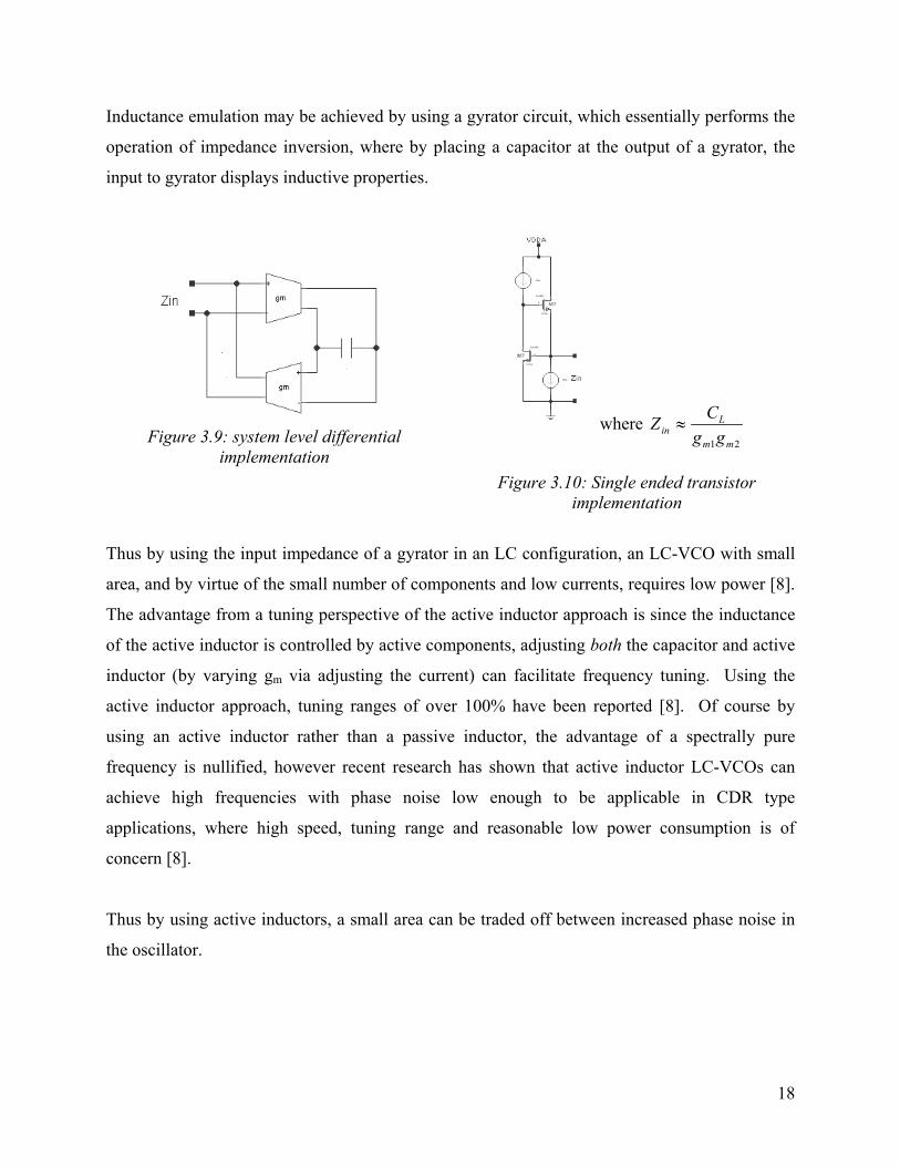
Inductance emulation may be achieved by using a gyrator circuit, which essentially performs the
operation of impedance inversion, where by placing a capacitor at the output of a gyrator, the
input to gyrator displays inductive properties.
Figure 3.9: system level differential
implementation
where 21 mm gg
Lin
CZ ≈
Figure 3.10: Single ended transistor
implementation
Thus by using the input impedance of a gyrator in an LC configuration, an LC-VCO with small
area, and by virtue of the small number of components and low currents, requires low power [8].
The advantage from a tuning perspective of the active inductor approach is since the inductance
of the active inductor is controlled by active components, adjusting both the capacitor and active
inductor (by varying gm via adjusting the current) can facilitate frequency tuning. Using the
active inductor approach, tuning ranges of over 100% have been reported [8]. Of course by
using an active inductor rather than a passive inductor, the advantage of a spectrally pure
frequency is nullified, however recent research has shown that active inductor LC-VCOs can
achieve high frequencies with phase noise low enough to be applicable in CDR type
applications, where high speed, tuning range and reasonable low power consumption is of
concern [8].
Thus by using active inductors, a small area can be traded off between increased phase noise in
the oscillator.
18

4. Future directions
As more and more applications push the boundaries of high-speed design, LC-VCOs are
becoming more common. Subsequently the rapid growth of research into the improvement of
wide frequency tuning structures for the use of compensating process variations, and allowing a
wide range of input frequencies to a CDR, will continue. In particular, as the vast majority of
LC-VCOs use monolithic inductors (as opposed to active inductors), research will continue to
improve on the characterization of the inductor. Presently the exact behavior of the monolithic
inductor is difficult to predict due to complex field interactions, as such making it difficult to
simulate and hence design for. As more knowledge of the monolithic inductor becomes
available, a better understanding of the trade offs and hence applicability of tuning techniques
will result.
Although wide range tuning techniques are useful in some applications such as DVI for LCD,
they are essentially a nuisance and bandage solution in RF circuits, where the problem of large
process variations of inductors and capacitors necessitates a wide tuning range. Hence future
research will consist primarily of finding ways to improve processing to improve inductor and
capacitor fabrication, such that passive components with small variations and high Qs in CMOS
processes can result. As RF/wireless applications make up the of the bulk of circuits that use
LC-VCOs, it is conceivable that if semiconductor processing can someday produce monolithic
inductors and capacitors accurately with low losses, there would be no real need for wide range
tuning in LC-VCOs for RF, hence cutting back on the active research in the field and/or shifting
the focus to design optimal ultra-wide frequency tuning techniques for applications similar to
DVI for LCD.
19
5. Conclusions
In this paper, a discussion of different tuning techniques for LC-VCOs was presented. It was
shown that depending on the power, phase noise, tuning range and area specifications of an
application different tuning techniques would have to be used. Specifically it was shown that for
RF/wireless applications, due to low power and noise constraints tuning was best achieved with
varactors. Varactor implementations currently popular, such as the I-MOS, and A-MOS were
highlighted. For CDR applications in DVI, it was shown that due to the demand for wider tuning
range and relaxed constraints on power and noise, a switched capacitor tuning technique could
be used. Modern approaches such as switched gain, and impedance transformation with
transformers were shown. To minimize area, it was shown that an active inductor could be used
to achieve low power and tuning range at the cost of increased phase noise. It was shown that
such an approach is best suited for CDR applications. The Future direction of research was
shown to involve the further development and enhancement of existing architectures as well as
an improvement of inductor modeling and device processing.
From the discussion of wide range tuning in LC-VCOs, one may appreciate the many tradeoffs
that govern tuning schemes. Most importantly, that:
• Low power, and phase noise are conflicting requirements with wide tuning range.
• Increased phase noise can be traded for reduced area
20

References:
[1] Thomas H. Lee S. Simon Wong, “CMOS RF Integrated Circuits 5GHz and Beyond”, Proceedings of the IEEE, vol 88, October 2000, pp.1560-1571 [2] Razavi, Behzad. Design of Analog CMOS Integrated Circuits. McGraw-Hill, New York, 2000 [3] Ali Hajimiri and Thomas H. Lee, “Phase Noise in CMOS Differential LC Oscillators”, 1998 Symposium on VLSI Circuits Digest of Technical Papers, 1998, pp.48-51 [4] Pietro Andreani and Sven Mattisson, “On the Use of MOS Varactors in RF VCO’s”, IEEE
Journal of Solid State Circuits, Brief Papers, June 2000, pp. 905-910
[5] A. Kral, F. Behbahani, A. Abidi, “RF-CMOS Oscillators with Switched Tuning”, IEEE 1998 Custom Integrated Circuits Conference, pp. 555-558 [6] I. Ahmed, “Wide-Frequency-Range Tuneable LC Oscillator”, Undergraduate Thesis, University of Toronto, 2002 [7] M. Bury, K.W. Martin, “A Wide-Tuning Range Transformer-Based RF CMOS Oscillator”, University of Toronto [8] T.Y.K. Lin and A.J. Payne, “Design of a Low-Voltage, Low-Power, Wide-Tuning Integrated Oscillator”, ISCAS 2000 – IEEE International Symposium on Circuits and systems, May 28-31 2000, pp. 629-630
21